IJCSIET--International Journal of Computer Science information and Engg., Technologies ISSN 2277-4408 || 01122014-009 IJCSIET - ISSUE4 - VOLUM E3 - SERIES3 Page 1 REALIZATION OF ENERGY EFFICIENT LOGIC CIRCUITS USING ADIABATIC TECHNIQUE S S KIRAN #1 , D. P. Raju #2 # Department of Electronics and Communication, KAUSHIK COLLEGE OF ENGINEERING ABSTRACT The Energy dissipation in conventional CMOS circuits can be minimized through adiabatic technique. By adiabatic technique dissipation in PMOS network can be minimized and some of energy stored at load capacitance can be recycled instead of dissipated as heat. But the adiabatic technique is highly dependent on parameter variation. The intension of the paper is to implement combinational and sequential logic gates such as AND, NAND, OR, NOR, XOR, XNOR and evaluate the various parameters obtained against each and every logic individually. This implementation is carried out by proper utilisation of various adiabatic techniques in the Microwind tool. The power consumption is greatly reduced in the proposed design of logic gates using adiabatic techniques. Index Terms— Adiabatic switching, energy dissipation, ECRL, PFAL, 2PASCL 1. INTRODUCTION At Earlier stages the JFET was predicted by Julius Lilienfeld in 1925 and by the mid-1930s its theory of operation was sufficiently well known to justify a patent. However, it was not possible for many years to make doped crystals with enough precision to show the effect. In 1947, researchers John Bardeen, Walter Houser Brattain, and William Shockley were trying to make a JFET when they discovered the point- contact transistor. The first practical JFETs were made many years later, in spite of their conception long before the junction transistor. To some extent it can be treated as a hybrid of a MOSFET (metal–oxide–semiconductor field- effect transistor).The idea of MOSFET was patented by J. E. Lilienfeld in the early 1930 Well before the invention of the Bi-polar transistor. Owing to fabrication limitations, however, MOS Technology was originally started in 1960 by Allen-Bradley to provide a second source for electronic calculators and their chips designed by Texas Instruments (TI). Later it lead a path to develop CMOS. CMOS devices were introduced, initiating a revolution in the semiconductor industry. Complementary metal–oxide– semiconductor (CMOS) is a technology for constructing integrated circuits. CMOS technology is used in micro processors, microcontrollers, static RAM, and other digital logic circuits. CMOS technology is also used for several analog circuits such as image sensors (CMOS sensor), data converters, and highly integrated transceivers for many types of communication. Frank Wanlass patented CMOS in 1963. In the early 1970s TI decided to release their own line of calculators, instead of selling just the chips inside them, and introduced them at a price that was lower than the price of the chipset alone. Many early chip companies were wiped out in the aftermath; those that survived did so by finding other chips to produce. MOS technologies became practical much later with the 1 st several generations, producing only n-Type transistors. Analog design is art and science at the same time. It is art because it requires creativity to strike the right compromises between the specifications imposed and the ones forgotten. It is also science because it requires a certain level of methodology to carry out a design, inevitably leading to more insight in the compromises taken.Analog circuit design is a very personalized discipline. Practitioners of analog design are noted for their individuality. The contemporary analog design has a founding father, George Philbrick. Back in the 1950’s, George Philbrick say, “digital is a special case of analog”. Linearity of real world phenomena has nothing to do with the analog versus digital question. The real (analog) world is full of non-linearities. Analog circuit design is described using terms such as subtractor, integrator, differentiator and summing junction. These mathematical operations are performed by that pillar of analoggery, the operational amplifier.Digital types insisted that analog techniques could never achieve any significant accuracy, regardless of how adopt were at modelling and simulating real systems. But the real world is analog in nature. To have something in digital there should be an analog circuit to convert the analog signals to digital form. Such conversion is possible with A/D converter.
Transcript
IJCSIET--International Journal of Computer Science information and Engg., Technologies ISSN 2277-4408 || 01122014-009
IJCSIET - ISSUE4 - VOLUM E3 - SERIES3 Page 1
REALIZATION OF ENERGY EFFICIENT LOGIC CIRCUITS USING ADIABATIC TECHNIQUE
S S KIRAN
#1, D. P. Raju
#2
# Department of Electronics and Communication, KAUSHIK COLLEGE OF ENGINEERING
ABSTRACT
The Energy dissipation in conventional CMOS circuits can be minimized through adiabatic technique. By adiabatic technique dissipation in PMOS network can be minimized and some of energy stored at load capacitance can be recycled instead of dissipated as heat. But the adiabatic technique is highly dependent on parameter variation. The intension of the paper is to implement combinational and sequential logic gates such as AND, NAND, OR, NOR, XOR, XNOR and evaluate the various parameters obtained against each and every logic individually. This implementation is carried out by proper utilisation of various adiabatic techniques in the Microwind tool. The power consumption is greatly reduced in the proposed design of logic gates using adiabatic techniques.
Index Terms— Adiabatic switching, energy
dissipation, ECRL, PFAL, 2PASCL 1. INTRODUCTION
At Earlier stages the JFET was predicted by Julius Lilienfeld in 1925 and by the mid-1930s its theory of operation was sufficiently well known to justify a patent. However, it was not possible for many years to make doped crystals with enough precision to show the effect. In 1947, researchers John Bardeen, Walter Houser Brattain, and William Shockley were trying to make a JFET when they discovered the point-contact transistor. The first practical JFETs were made many years later, in spite of their conception long before the junction transistor. To some extent it can be treated as a hybrid of a MOSFET (metal–oxide–semiconductor field-effect transistor).The idea of MOSFET was patented by J. E. Lilienfeld in the early 1930 Well before the invention of the Bi-polar transistor. Owing to fabrication limitations, however, MOS Technology was originally started in 1960 by Allen-Bradley to provide a second source for electronic calculators and their chips designed by Texas Instruments (TI). Later it lead a path to develop CMOS. CMOS devices were introduced, initiating a revolution in the semiconductor industry.
Complementary metal–oxide–semiconductor (CMOS) is a technology for constructing integrated circuits. CMOS technology is used in micro
processors, microcontrollers, static RAM, and other digital logic circuits. CMOS technology is also used for several analog circuits such as image sensors (CMOS sensor), data converters, and highly integrated transceivers for many types of communication. Frank Wanlass patented CMOS in 1963. In the early 1970s TI decided to release their own line of calculators, instead of selling just the chips inside them, and introduced them at a price that was lower than the price of the chipset alone. Many early chip companies were wiped out in the aftermath; those that survived did so by finding other chips to produce. MOS technologies became practical much later with the 1
st several generations, producing only
n-Type transistors. Analog design is art and science at the
same time. It is art because it requires creativity to strike the right compromises between the specifications imposed and the ones forgotten. It is also science because it requires a certain level of methodology to carry out a design, inevitably leading to more insight in the compromises taken.Analog circuit design is a very personalized discipline. Practitioners of analog design are noted for their individuality. The contemporary analog design has a founding father, George Philbrick. Back in the 1950’s, George Philbrick say, “digital is a special case of analog”. Linearity of real world phenomena has nothing to do with the analog versus digital question. The real (analog) world is full of non-linearities. Analog circuit design is described using terms such as subtractor, integrator, differentiator and summing junction. These mathematical operations are performed by that pillar of analoggery, the operational amplifier.Digital types insisted that analog techniques could never achieve any significant accuracy, regardless of how adopt were at modelling and simulating real systems. But the real world is analog in nature. To have something in digital there should be an analog circuit to convert the analog signals to digital form. Such conversion is possible with A/D converter.
IJCSIET--International Journal of Computer Science information and Engg., Technologies ISSN 2277-4408 || 01122014-009
IJCSIET - ISSUE4 - VOLUM E3 - SERIES3 Page 2
Fig 1: MOS device dimension scaling trends
Fig 2: voltage supply trends
2. ADIABATIC LOGIC
Power consumption plays an important role in the present day VLSI technology. As many of the present day electronic devices are portable, they need more battery backup which can be achieved only with the low power consumption circuits that are internally designed in them. So energy efficiency has become main concern in the portable equipments to get better performance with less power dissipation. As the power dissipation in a device increases then extra circuitry is necessary to cool the device and to protect the device from thermal breakdown which also results in increase of total area of the device. In order to overcome these problems the power dissipation of the circuit is to be reduced by adopting different low power techniques. The less the power dissipation, the more efficient the circuit will work.
From the past few decades CMOS technology plays a dominant role in designing low power consuming devices. Compared to different logic families CMOS has less power dissipation which made it superior over the previous low power techniques. The power consumption in conventional CMOS circuit is due to switching activity of the devices from one state to another state and due to the charging and discharging of load capacitor at the output node. The power dissipation in conventional CMOS design can be
minimized by reducing the supply voltage, node capacitance value and switching activity. But reducing the values of these parameters may degrade the performance of the device.
So an efficient low power technique other than CMOS is needed that has less power dissipation compared to CMOS which can be done by using adiabatic technique. Adiabatic logic is an energy efficient charge recovery logic which is a thermodynamic process that exchanges no heat with the environment. Reduction of power dissipation occurs at the cost of slower speed of operation. It also allows the recycling of energy to reduce the total energy drawn from the power source.Adiabatic design is developed to overcome the power dissipation problems in CMOS design which is the most concern aspect in present day VLSI technology. Adiabatic logic is implemented by placing two AC sources in which one source is out of phase with the other and two sources are connected to ground. The recovery process can be done in such a way that the charge is stored in capacitor while charging phase and while discharging the energy is recycled by the second AC source and again used in the circuit. The adiabatic design can be shown as follows
Fig. 3: Adiabatic charging and discharging
3 ADIABATIC TECHNIQUES:
Adiabatic logic has a different logic style which helps in the reduction of the power dissipation of the circuit. Some of the important adiabatic techniques are
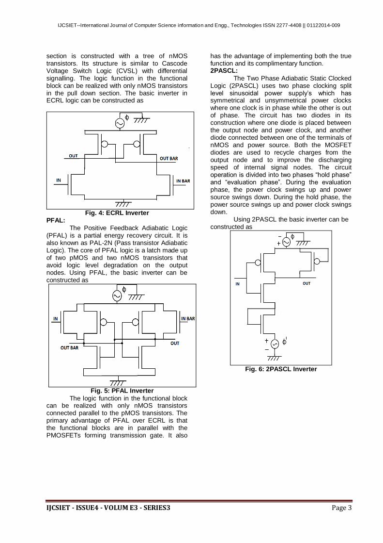
ECRL:
Efficient charge recovery logic (ECRL) consists of two cross couple pMOS transistors in the pull up section where as the pull down
IJCSIET--International Journal of Computer Science information and Engg., Technologies ISSN 2277-4408 || 01122014-009
IJCSIET - ISSUE4 - VOLUM E3 - SERIES3 Page 3
section is constructed with a tree of nMOS transistors. Its structure is similar to Cascode Voltage Switch Logic (CVSL) with differential signalling. The logic function in the functional block can be realized with only nMOS transistors in the pull down section. The basic inverter in ECRL logic can be constructed as
Fig. 4: ECRL Inverter
PFAL:
The Positive Feedback Adiabatic Logic (PFAL) is a partial energy recovery circuit. It is also known as PAL-2N (Pass transistor Adiabatic Logic). The core of PFAL logic is a latch made up of two pMOS and two nMOS transistors that avoid logic level degradation on the output nodes. Using PFAL, the basic inverter can be constructed as
Fig. 5: PFAL Inverter
The logic function in the functional block can be realized with only nMOS transistors connected parallel to the pMOS transistors. The primary advantage of PFAL over ECRL is that the functional blocks are in parallel with the PMOSFETs forming transmission gate. It also
has the advantage of implementing both the true function and its complimentary function. 2PASCL:
The Two Phase Adiabatic Static Clocked Logic (2PASCL) uses two phase clocking split level sinusoidal power supply’s which has symmetrical and unsymmetrical power clocks where one clock is in phase while the other is out of phase. The circuit has two diodes in its construction where one diode is placed between the output node and power clock, and another diode connected between one of the terminals of nMOS and power source. Both the MOSFET diodes are used to recycle charges from the output node and to improve the discharging speed of internal signal nodes. The circuit operation is divided into two phases “hold phase” and “evaluation phase”. During the evaluation phase, the power clock swings up and power source swings down. During the hold phase, the power source swings up and power clock swings down. Using 2PASCL the basic inverter can be constructed as
Fig. 6: 2PASCL Inverter
IJCSIET--International Journal of Computer Science information and Engg., Technologies ISSN 2277-4408 || 01122014-009
IJCSIET - ISSUE4 - VOLUM E3 - SERIES3 Page 4
4 WAVEFORMS AND DIAGRAMS:
Fig. 7: Schematic diagram of Adiabatic D-flip flop (ECRL)
Fig. 8: Layout of Adiabatic D-flip flop (ECRL)
IJCSIET--International Journal of Computer Science information and Engg., Technologies ISSN 2277-4408 || 01122014-009
IJCSIET - ISSUE4 - VOLUM E3 - SERIES3 Page 5
Fig. 9: Schematic diagram of Adiabatic D-flip flop (PFAL)
Fig. 10: Layout of Adiabatic D-flip flop (PFAL)
IJCSIET--International Journal of Computer Science information and Engg., Technologies ISSN 2277-4408 || 01122014-009
IJCSIET - ISSUE4 - VOLUM E3 - SERIES3 Page 6
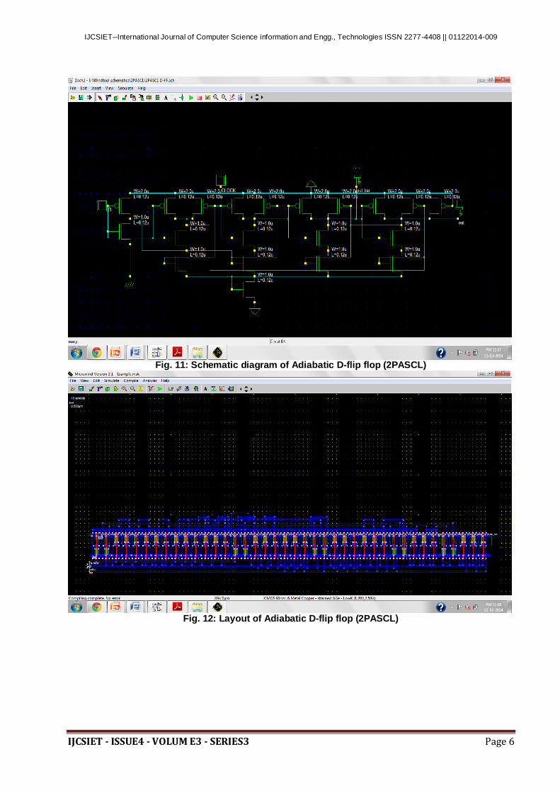
Fig. 11: Schematic diagram of Adiabatic D-flip flop (2PASCL)
Fig. 12: Layout of Adiabatic D-flip flop (2PASCL)
IJCSIET--International Journal of Computer Science information and Engg., Technologies ISSN 2277-4408 || 01122014-009
IJCSIET - ISSUE4 - VOLUM E3 - SERIES3 Page 7
Fig. 13: Adiabatic ECRL D-flip flop waveform
Fig. 14: Adiabatic PFAL D-flip flop waveform
IJCSIET--International Journal of Computer Science information and Engg., Technologies ISSN 2277-4408 || 01122014-009
IJCSIET - ISSUE4 - VOLUM E3 - SERIES3 Page 8
Fig. 15: Adiabatic 2PASCL D-flip flop waveform
5. RESULTS
Table 1 Parameters of Conventional Model of Combinational & Sequential Circuits
IJCSIET--International Journal of Computer Science information and Engg., Technologies ISSN 2277-4408 || 01122014-009
IJCSIET - ISSUE4 - VOLUM E3 - SERIES3 Page 9
Fig. 16 Graphical representation of Conventional CMOS LOGIC
Table 2 Parameters of Adiabatic ECRL Model of Combinational & Sequential Circuits
IJCSIET--International Journal of Computer Science information and Engg., Technologies ISSN 2277-4408 || 01122014-009
IJCSIET - ISSUE4 - VOLUM E3 - SERIES3 Page 10
Fig. 17 Graphical representation of Adiabatic ECRL LOGIC
Table 3 Parameters of Adiabatic PFAL Model of Combinational & Sequential Circuits
IJCSIET--International Journal of Computer Science information and Engg., Technologies ISSN 2277-4408 || 01122014-009
IJCSIET - ISSUE4 - VOLUM E3 - SERIES3 Page 11
Fig. 18 Graphical representation of Adiabatic PFAL LOGIC
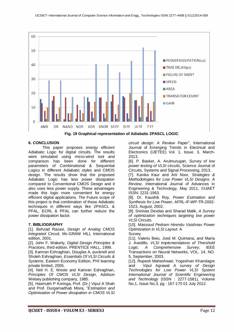
Table 4 Parameters of Adiabatic 2PASCL Model of Combinational & Sequential Circuits
IJCSIET--International Journal of Computer Science information and Engg., Technologies ISSN 2277-4408 || 01122014-009
IJCSIET - ISSUE4 - VOLUM E3 - SERIES3 Page 12
Fig. 19 Graphical representation of Adiabatic 2PASCL LOGIC
6. CONCLUSION
This paper proposes energy efficient Adiabatic Logic for digital circuits. The results were simulated using micro-wind tool and comparison has been done for different parameters of Combinational & Sequential Logics in different Adiabatic styles and CMOS design. The results show that the proposed Adiabatic Logic has less power dissipation compared to Conventional CMOS Design and it also uses less power supply. These advantages made this logic more convenient for energy efficient digital applications. The Future scope of this project is that combination of these Adiabatic techniques in different ways like 2PASCL & PFAL, ECRL & PFAL can further reduce the power dissipation factor. 7. BIBLIOGRAPHY
[1]. Behzad Razavi, Design of Analog CMOS Integrated Circuit, Mc-GRAW HILL International edition, 2001. [2]. John F. Wakerly, Digital Design Principles & Practices, third edition, PRENTICE HALL, 1999. [3]. Kamran Eshraghian, Douglas A. pucknell and Sholeh Eshraghian, Essentials Of VLSI Circuits & Systems, Eastern Economy Edition, PHI learning private limited, 2005. [4]. Neil H. E. Weste and Kamran Eshraghian, Principles Of CMOS VLSI Design, Addison Welsey publishing company, 1985. [5]. Hasmukh P Koringa, Prof. (Dr.) Vipul A Shah and Prof. Durgamadhab Misra, “Estimation and Optimization of Power dissipation in CMOS VLSI