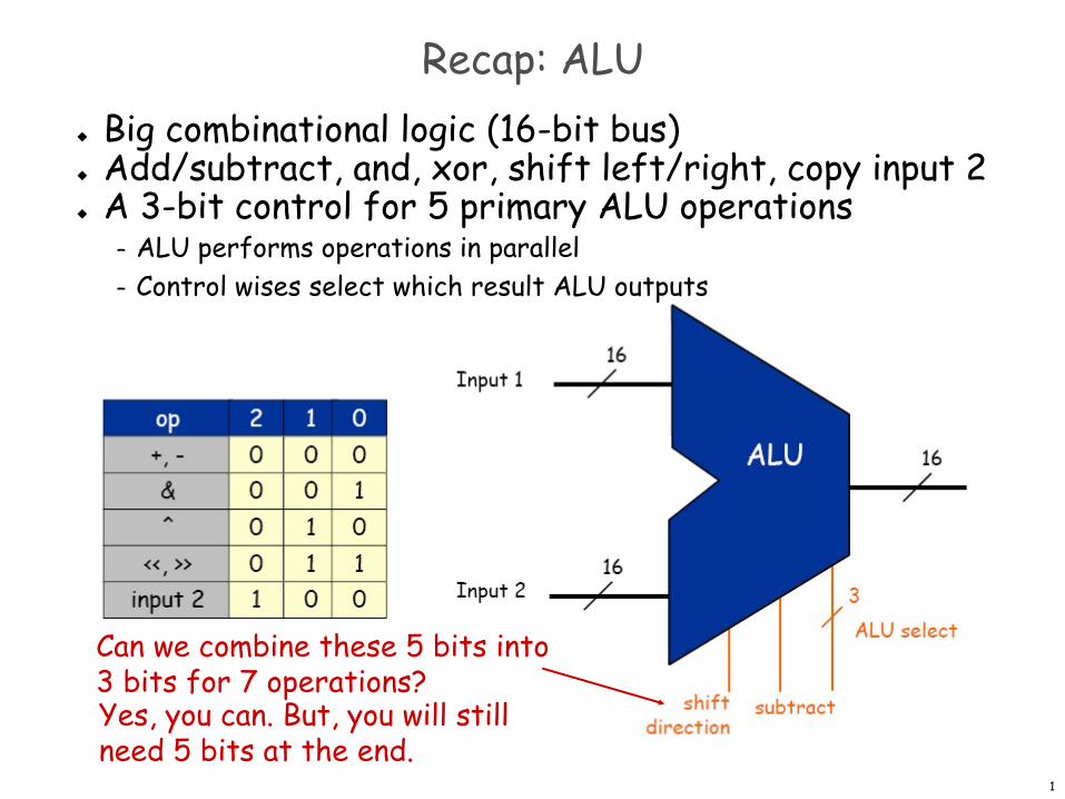
1 Recap: ALU u Big combinational logic (16-bit bus) u Add/subtract, and, xor, shift left/right, copy input 2 u A 3-bit control for 5 primary ALU operations – ALU performs operations in parallel – Control wises select which result ALU outputs Can we combine these 5 bits into 3 bits for 7 operations? Yes, you can. But, you will still need 5 bits at the end.
Transcript
1
Recap: ALUu Big combinational logic (16-bit bus)u Add/subtract, and, xor, shift left/right, copy input 2u A 3-bit control for 5 primary ALU operations
– ALU performs operations in parallel– Control wises select which result ALU outputs
Can we combine these 5 bits into 3 bits for 7 operations?Yes, you can. But, you will still need 5 bits at the end.
2
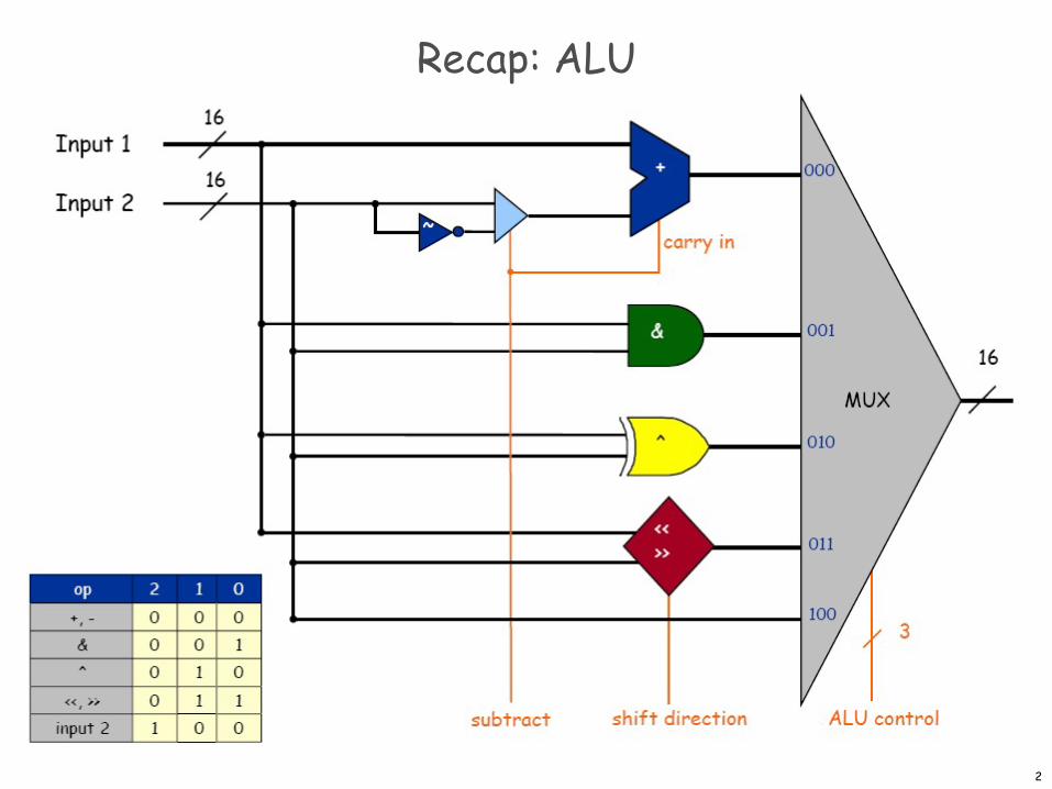
Recap: ALU
3
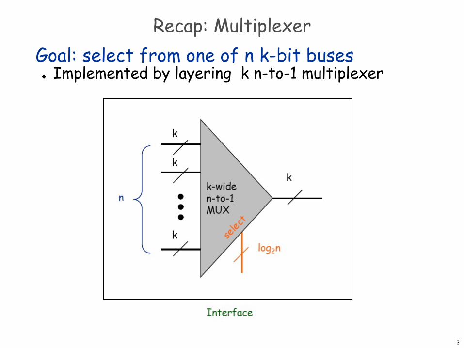
Goal: select from one of n k-bit busesu Implemented by layering k n-to-1 multiplexer
Recap: Multiplexer
4
Recap: flip flop
5
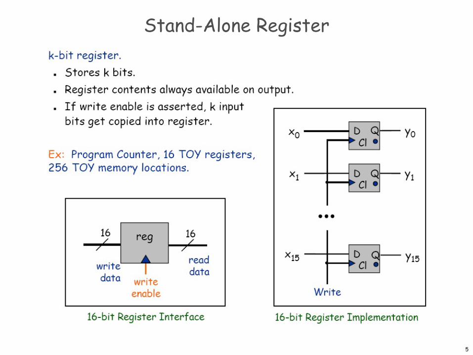
Stand-Alone Register
6
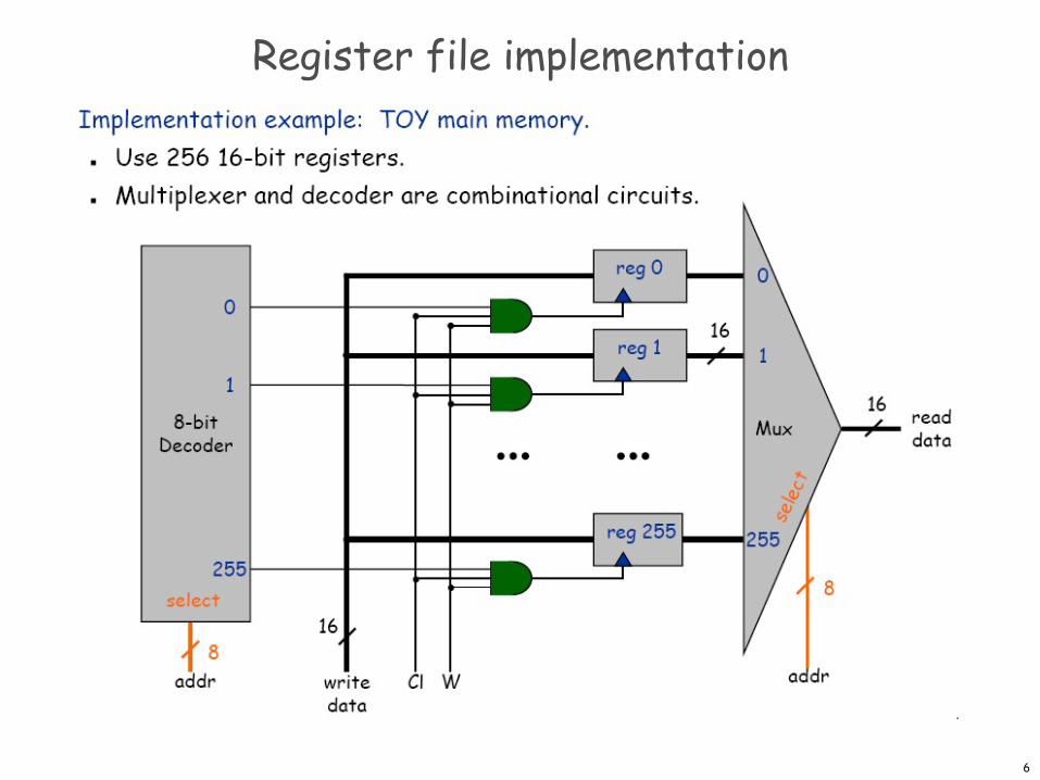
Register file implementation
7
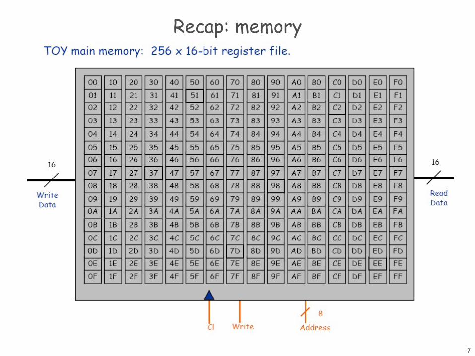
Recap: memory
8
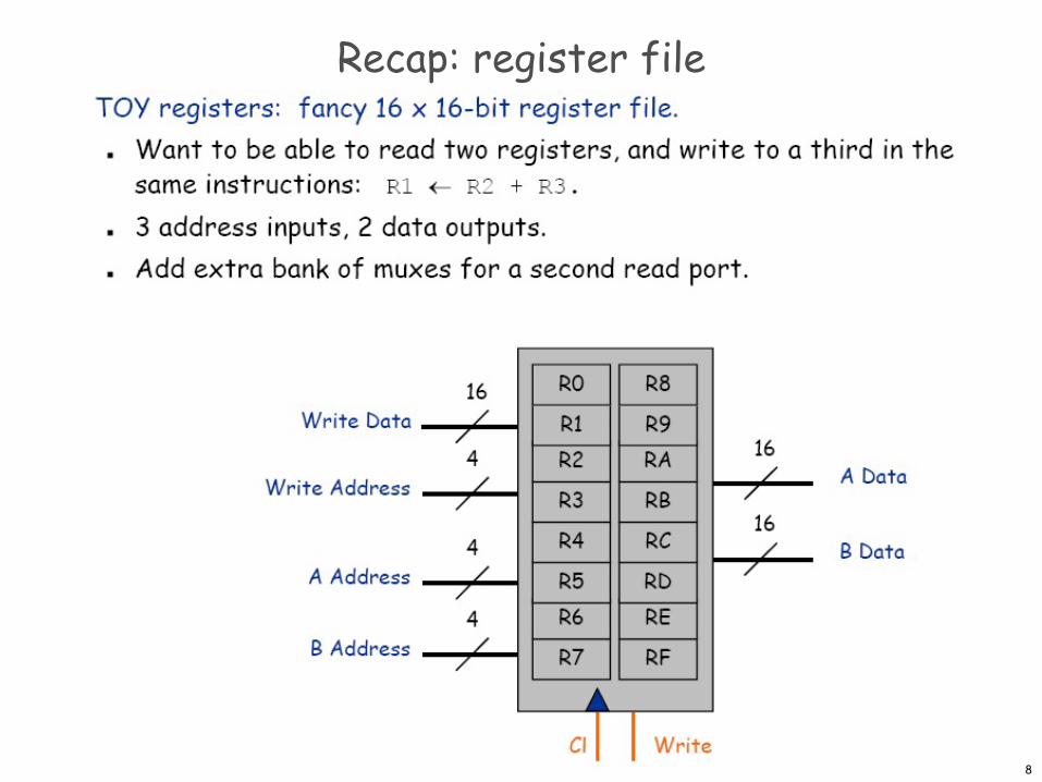
Recap: register file
9
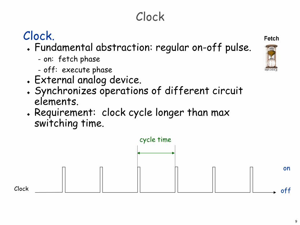
ClockClock.
u Fundamental abstraction: regular on-off pulse.– on: fetch phase– off: execute phase
u External analog device.u Synchronizes operations of different circuit
elements.u Requirement: clock cycle longer than max
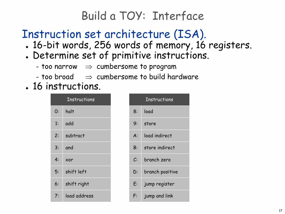
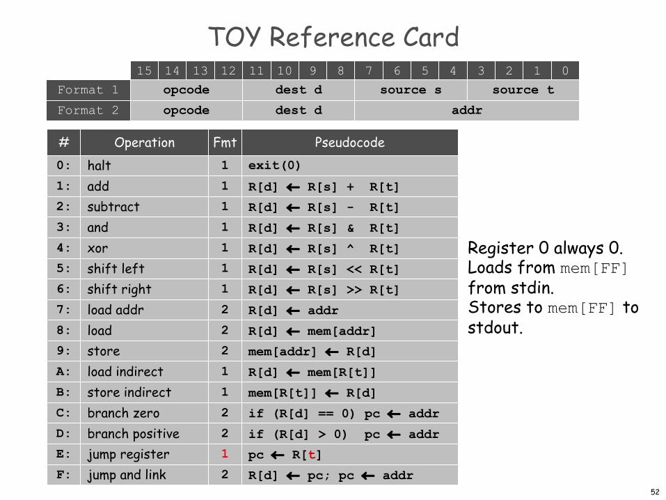
8: load9: storeA: load indirectB: store indirectC: branch zeroD: branch positiveE: jump registerF: jump and link
R[d] ¬ mem[addr]
mem[addr] ¬ R[d]
R[d] ¬ mem[R[t]]
mem[R[t]] ¬ R[d]
if (R[d] == 0) pc ¬ addr
if (R[d] > 0) pc ¬ addr
pc ¬ R[t]
R[d] ¬ pc; pc ¬ addr
13 12 11 1015 14 7 69 8 6 4 1 03 25
opcode dest d addr
opcode dest d source s source t
Format 2
Format 1
Operation Pseudocode1
Fmt
1
1
1
1
1
1
2
2
2
1
1
2
2
1
2
Register 0 always 0.Loads from mem[FF]from stdin.Stores to mem[FF] to stdout.
19
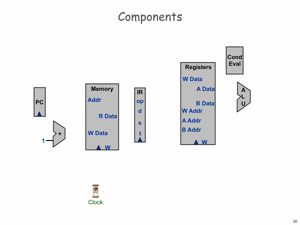
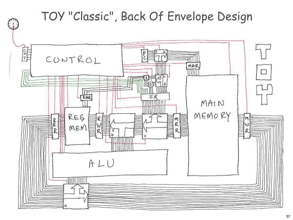
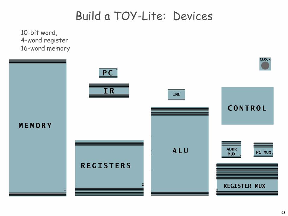
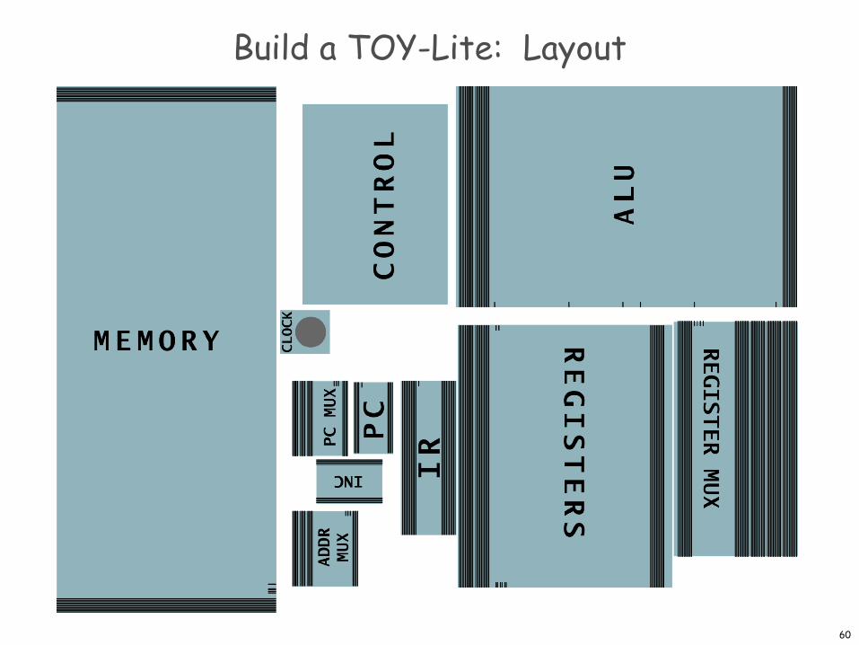
Design a processorHow to build a processor
u Develop instruction set architecture (ISA)– 16-bit words, 16 TOY machine instructions
u Determine major components– ALU, memory, registers, program counter
u Determine datapath requirements– Flow of bits
u Analyze how to implement each instruction– Determine settings of control signals
20
Components
PC
Registers
W
W DataA Data
B DataW AddrA AddrB Addr+
1
Memory
W
W Data
Addr
R Data
IRopd
s
t
ALU
Clock
CondEval
21
Cond. Eval.
CondEval
16X
Y0
Y1
=0
>0
Y0
Y1
X0
X15:
Y1=x>0=(x³0) and (x¹0)=X15 ÙY0
22
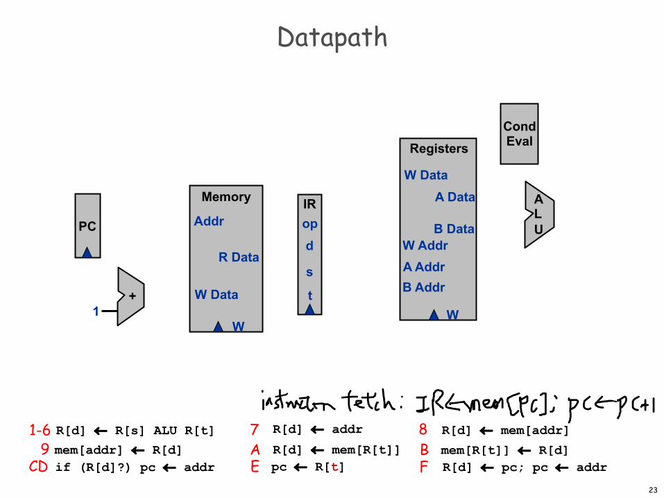
Design a processorHow to build a processor
u Develop instruction set architecture (ISA)– 16-bit words, 16 TOY machine instructions
u Determine major components– ALU, memory, registers, program counter
u Determine datapath requirements– Flow of bits
u Analyze how to implement each instruction– Determine settings of control signals
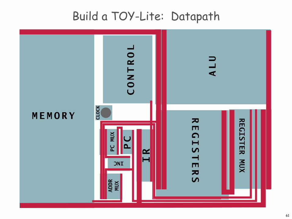
23
Datapath
PC
Registers
W
W DataA Data
B DataW AddrA AddrB Addr+
1
Memory
W
W Data
Addr
R Data
IRopd
s
t
ALU
R[d] ¬ R[s] ALU R[t] R[d] ¬ addr R[d] ¬ mem[addr]
mem[addr] ¬ R[d] R[d] ¬ mem[R[t]] mem[R[t]] ¬ R[d]if (R[d]?) pc ¬ addr pc ¬ R[t] R[d] ¬ pc; pc ¬ addr
1-6 7 89 A B
CD E F
CondEval
24
Datapath
PC
Registers
W
W DataA Data
B DataW AddrA AddrB Addr+
1
Memory
W
W Data
Addr
R Data
IRopd
s
t
CondEval
ALU
pc+1
pc for jumpand branch
address for load/store
result of ALU or address for load address
pc for jal
addr
store data
load
8 16
16
80
80
8
25
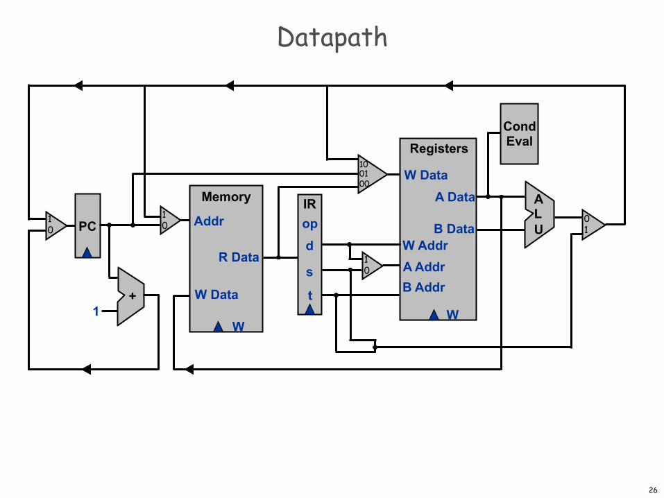
Design a processorHow to build a processor
u Develop instruction set architecture (ISA)– 16-bit words, 16 TOY machine instructions
u Determine major components– ALU, memory, registers, program counter
u Determine datapath requirements– Flow of bits
u Analyze how to implement each instruction– Determine settings of control signals
26
Datapath
PC
Registers
W
W DataA Data
B DataW AddrA AddrB Addr+
1
Memory
W
W Data
Addr
R Data
IRopd
s
t
CondEval
ALU
10
10
01
10
100100
27
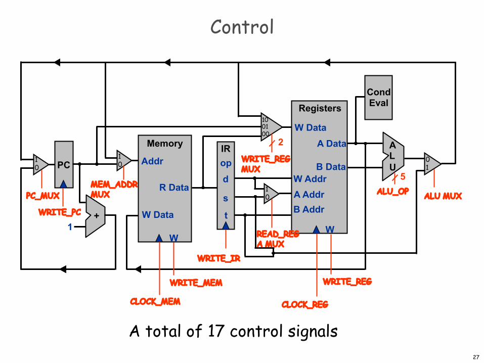
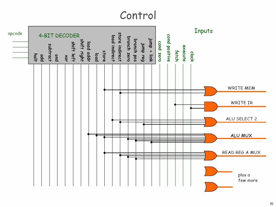
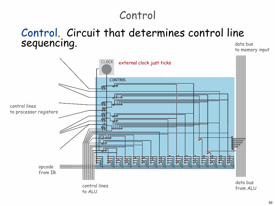
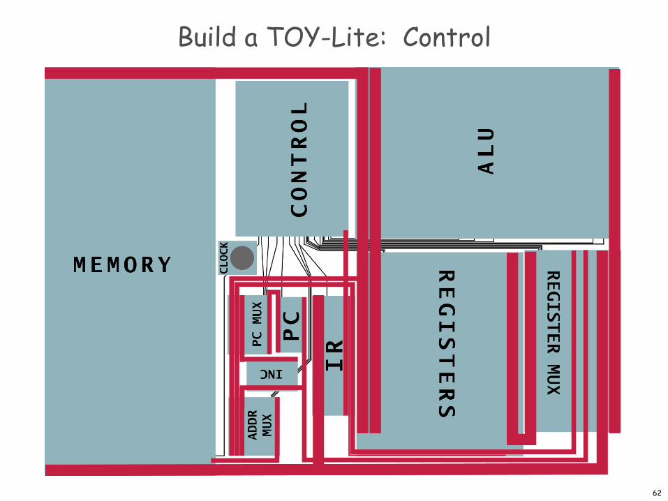
Control
PC
Registers
W
W DataA Data
B DataW AddrA AddrB Addr+
1
Memory
W
W Data
Addr
R Data
IRopd
s
t
CondEval
ALU
2
5
WRITE_MEM
WRITE_IR
CLOCK_MEM CLOCK_REG
WRITE_REG
ALU_OP
READ_REGA MUX
WRITE_REGMUX
MEM_ADDRMUX
WRITE_PC
PC_MUX ALU MUX
A total of 17 control signals
10
10
01
10
100100
28
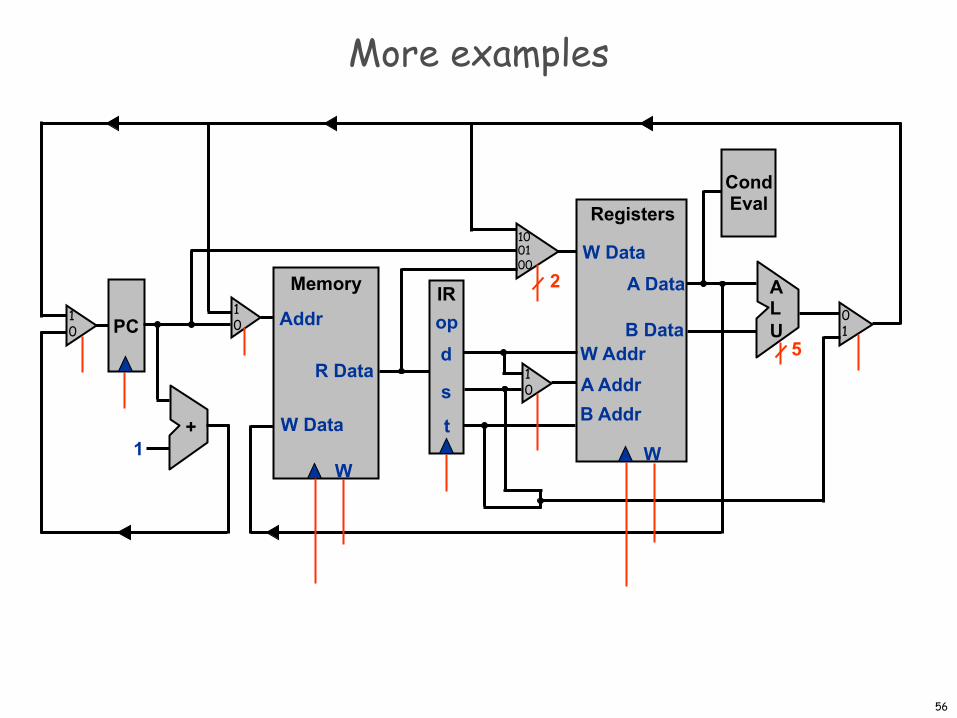
TOY architecture
PC
Registers
W
W DataA Data
B DataW AddrA AddrB Addr+
1-bitcounter
1
5
2
4
=0
>0
OpcodeExecuteFetchClock
Memory
W
W Data
Addr
R Data
IRopd
s
t
CondEval
ALU
ControlClock
10
10
01
10
100100
29
Clock
PC
Registers
W
W DataA Data
B DataW AddrA AddrB Addr+
1-bitcounter
1
5
2
4
=0
>0
OpcodeExecuteFetchClock
Memory
W
W Data
Addr
R Data
IRopd
s
t
CondEval
ALU
ControlClock
10
10
01
10
100100
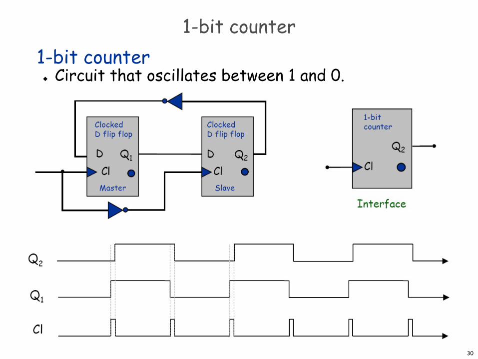
30
1-bit counter1-bit counter
u Circuit that oscillates between 1 and 0.
31
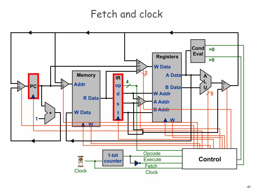
ClockTwo cycle design (fetch and execute)
u Use 1-bit counter to distinguish between 2 cycles.u Use two cycles since fetch and execute phases
each access memory and alter program counter.
32
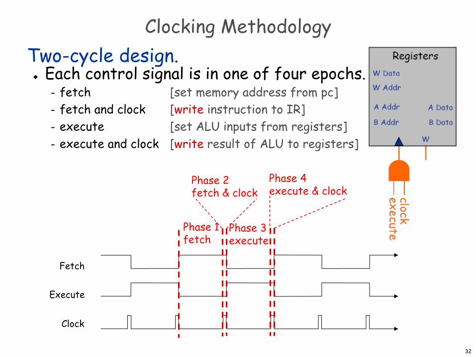
Clocking MethodologyTwo-cycle design.
u Each control signal is in one of four epochs.– fetch [set memory address from pc]– fetch and clock [write instruction to IR]– execute [set ALU inputs from registers]– execute and clock [write result of ALU to registers]
Fetch
Clock
Execute
Fetch
Phase 1fetch
Phase 3execute
Phase 2fetch & clock
Phase 4execute & clock
33
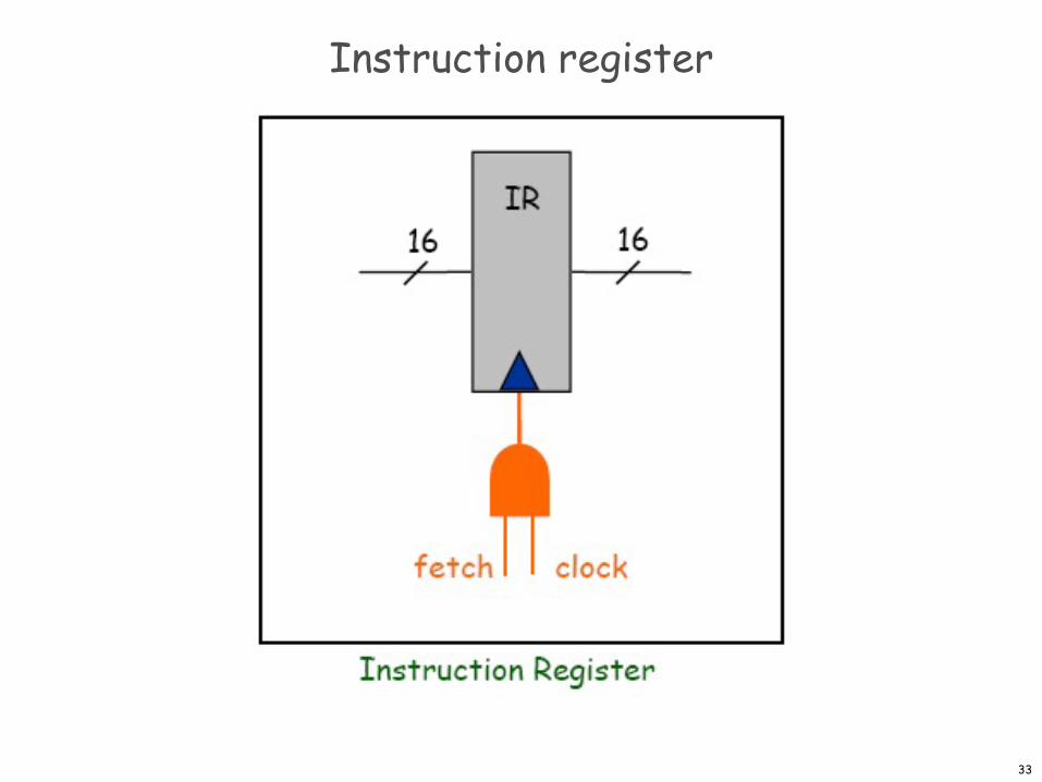
Instruction register
34
Clocking Methodology
PC
Registers
W
W DataA Data
B DataW AddrA AddrB Addr+
1
Memory
W
W Data
Addr
R Data
IRopd
s
t
CondEval
ALU
2
5
fetch execute
10
10
01
10
100100
35
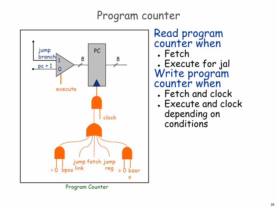
Program counterRead program counter when
u Fetchu Execute for jal
Write program counter when
u Fetch and clocku Execute and clock
depending on conditions
36
Example: ADD
PC
Registers
W
W DataA Data
B DataW AddrA AddrB Addr+
1
Memory
W
W Data
Addr
R Data
IRopd
s
t
CondEval
ALU
2
5
PC=20Mem[20]=1234R[3]=0028 R[4]=0064
20 ????
10
10
01
10
100100
37
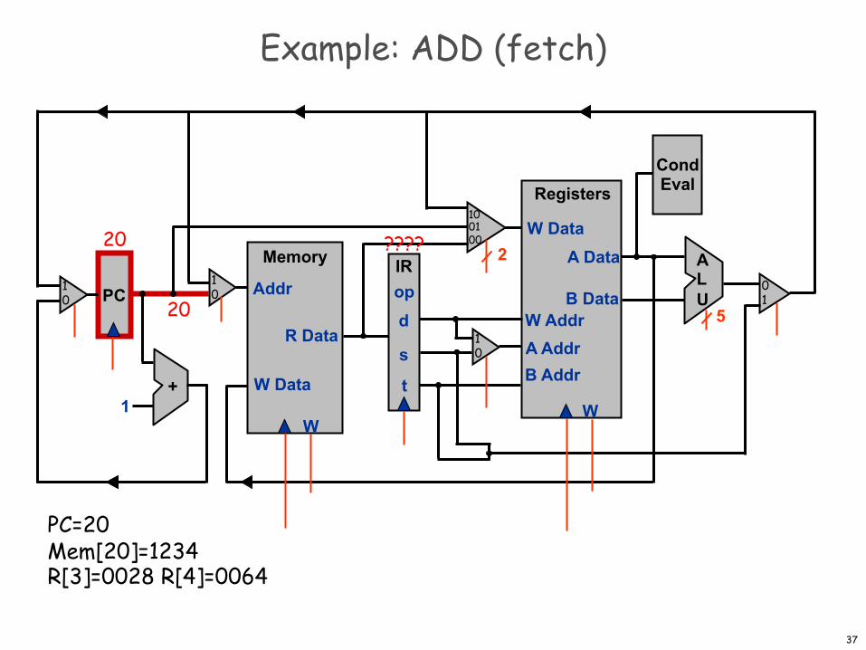
Example: ADD (fetch)
PC
Registers
W
W DataA Data
B DataW AddrA AddrB Addr+
1
Memory
W
W Data
Addr
R Data
IRopd
s
t
CondEval
ALU
2
520
????20
PC=20Mem[20]=1234R[3]=0028 R[4]=0064
10
10
01
10
100100
38
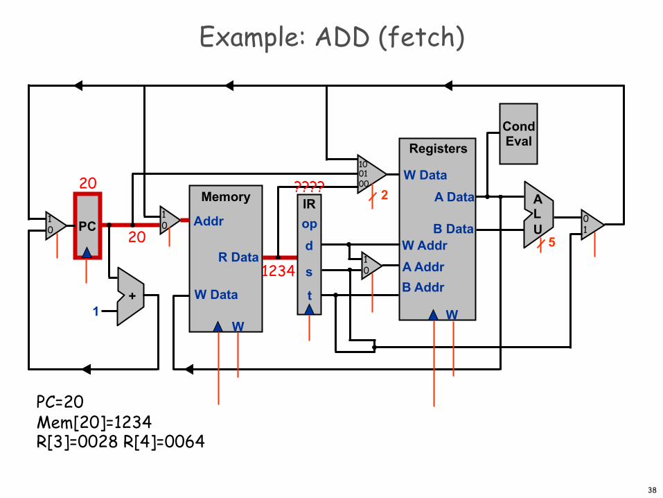
Example: ADD (fetch)
PC
Registers
W
W DataA Data
B DataW AddrA AddrB Addr+
1
Memory
W
W Data
Addr
R Data
IRopd
s
t
CondEval
ALU
2
520
1234
20 ????
PC=20Mem[20]=1234R[3]=0028 R[4]=0064
10
10
01
10
100100
39
Example: ADD (fetch)
PC
Registers
W
W DataA Data
B DataW AddrA AddrB Addr+
1
Memory
W
W Data
Addr
R Data
IRopd
s
t
CondEval
ALU
2
520
1234
21
20 ????
21
PC=20Mem[20]=1234R[3]=0028 R[4]=0064
10
10
01
10
100100
40
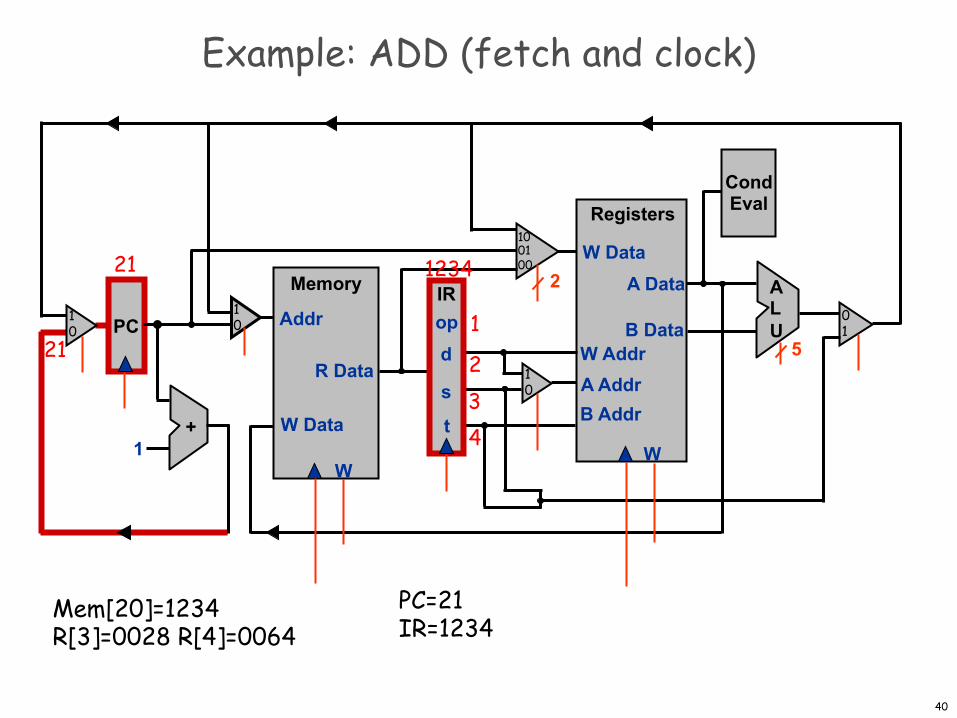
Example: ADD (fetch and clock)
PC
Registers
W
W DataA Data
B DataW AddrA AddrB Addr+
1
Memory
W
W Data
Addr
R Data
IRopd
s
t
CondEval
ALU
2
5
PC=21IR=1234
21 1234
211
234
Mem[20]=1234R[3]=0028 R[4]=0064
10
10
01
10
100100
41
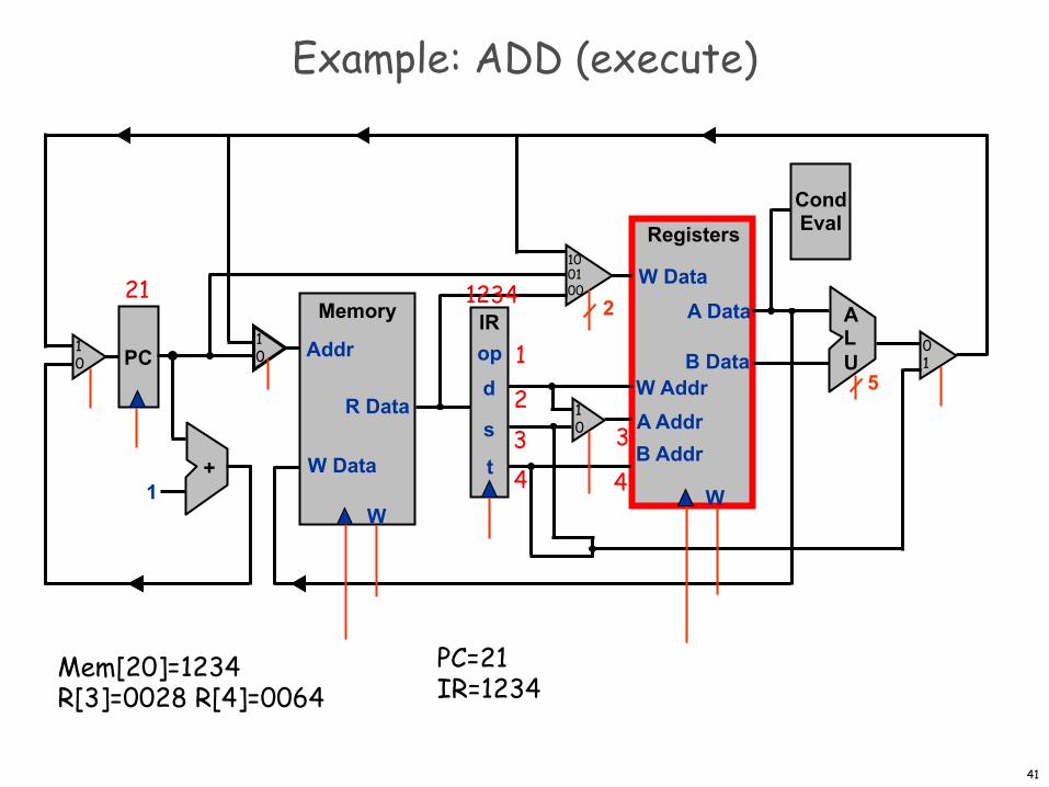
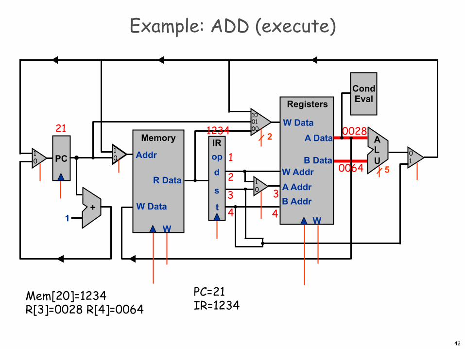
Example: ADD (execute)
PC
Registers
W
W DataA Data
B DataW AddrA AddrB Addr+
1
Memory
W
W Data
Addr
R Data
IRopd
s
t
CondEval
ALU
2
5
21 1234
1
234
PC=21IR=1234
Mem[20]=1234R[3]=0028 R[4]=0064
3
4
10
10
01
10
100100
42
Example: ADD (execute)
PC
Registers
W
W DataA Data
B DataW AddrA AddrB Addr+
1
Memory
W
W Data
Addr
R Data
IRopd
s
t
CondEval
ALU
2
5
21 1234
1
234
PC=21IR=1234
Mem[20]=1234R[3]=0028 R[4]=0064
0028
4
0064
3
10
10
01
10
100100
43
0064
0028
Example: ADD (execute)
PC
Registers
W
W DataA Data
B DataW AddrA AddrB Addr+
1
Memory
W
W Data
Addr
R Data
IRopd
s
t
CondEval
ALU
2
5
21 1234
1
234
PC=21IR=1234
Mem[20]=1234R[3]=0028 R[4]=0064
4
3
008C
008C
10
10
01
10
100100
44
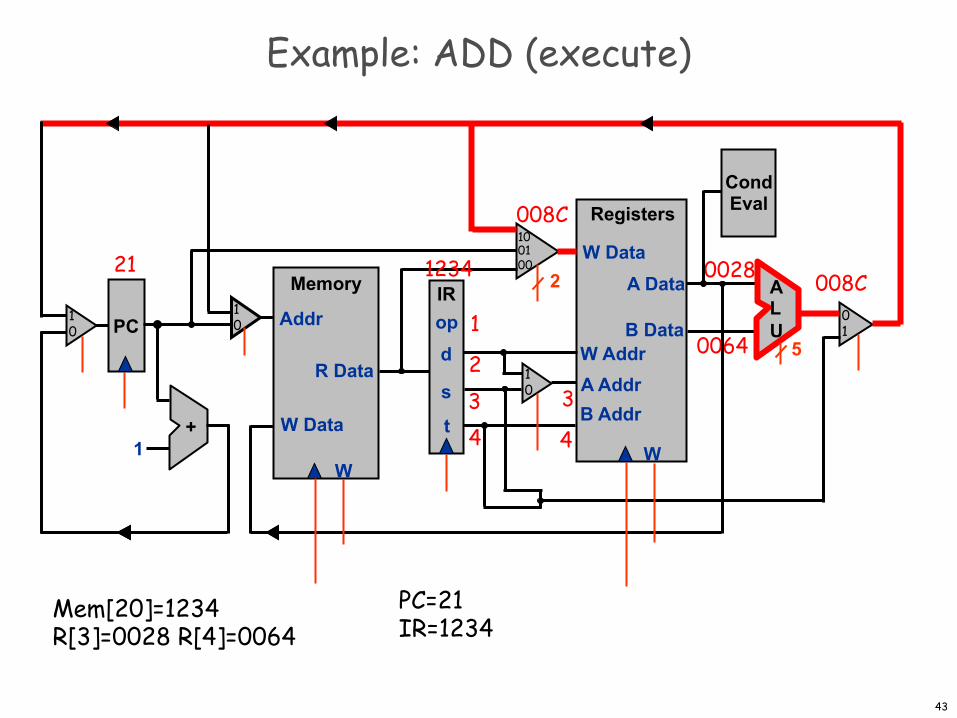
Example: ADD (execute and clock)
PC
Registers
W
W DataA Data
B DataW AddrA AddrB Addr+
1
Memory
W
W Data
Addr
R Data
IRopd
s
t
CondEval
ALU
2
5
21 1234
1
234
PC=21IR=1234R[2]=008C
Mem[20]=1234R[3]=0028 R[4]=0064
008C
2
10
10
01
10
100100
45
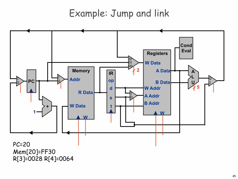
Example: Jump and link
PC
Registers
W
W DataA Data
B DataW AddrA AddrB Addr+
1
Memory
W
W Data
Addr
R Data
IRopd
s
t
CondEval
ALU
2
5
PC=20Mem[20]=FF30R[3]=0028 R[4]=0064
10
10
01
10
100100
46
Fetch
PC
Registers
W
W DataA Data
B DataW AddrA AddrB Addr+
1-bitcounter
1
5
2
4
=0
>0
OpcodeExecuteFetchClock
Memory
W
W Data
Addr
R Data
IRopd
s
t
CondEval
ALU
ControlClock
10
10
01
10
100100
47
Fetch and clock
PC
Registers
W
W DataA Data
B DataW AddrA AddrB Addr+
1-bitcounter
1
5
2
4
=0
>0
OpcodeExecuteFetchClock
Memory
W
W Data
Addr
R Data
IRopd
s
t
CondEval
ALU
ControlClock
10
10
01
10
100100
48
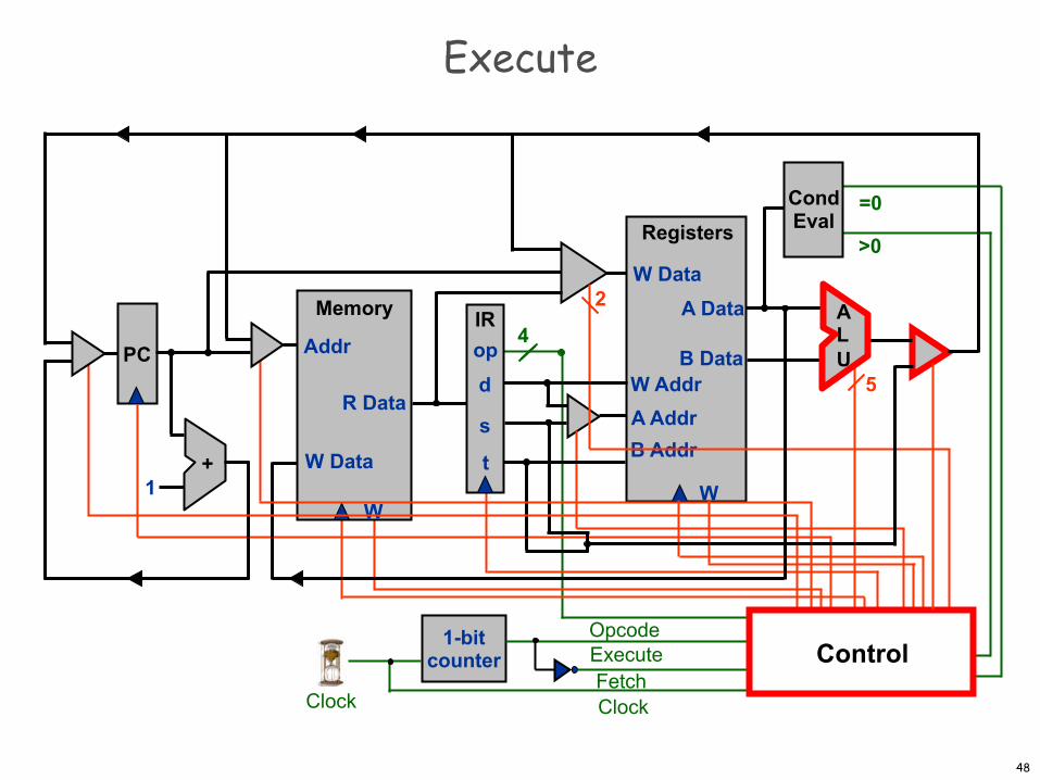
Execute
PC
Registers
W
W DataA Data
B DataW AddrA AddrB Addr+
1-bitcounter
1
5
2
4
=0
>0
OpcodeExecuteFetchClock
Memory
W
W Data
Addr
R Data
IRopd
s
t
CondEval
ALU
ControlClock
49
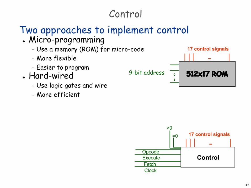
ControlTwo approaches to implement control
u Micro-programming– Use a memory (ROM) for micro-code– More flexible– Easier to program
u Hard-wired– Use logic gates and wire – More efficient