Location of ADC (A/D-converter) 1. Baseband or low IF
2. IF
3. RF Analog front-end bandwidth - ADC bandwidth 1. Single channel
2. Few channels
3. Frequency slice
4. Service band (e.g., GSM)
5. Frequency band (like 2 GHz range) The bandwidths of the analog front-end and ADC may or may not go hand in hand. Some examples below.
Receiver Architectures – Part 2 TLT-5806/RxArch2/3 M. Renfors, TUT/DCE 01.10.08
Narrowband front-end Per-channel down-conversion (0, or IF)
- Selectivity in analog part, good IF filters needed. - "Normal" frequency sythesizer needed. - No big demands for ADC dynamic range or jitter. - Sampling rate requirements are such that it is enough
to attenuate aliasing to the desired band. - Narrowband (baseband or bandpass) ADC (like ΣΔ)
Receiver Architectures – Part 2 TLT-5806/RxArch2/4 M. Renfors, TUT/DCE 01.10.08
Wideband front-end, per-channel down-conversion so that desired channel is around a fixed center frequency (0 or IF)
- Analog front-end simplified in the sense that highly selective IF filters are not needed.
- "Normal" frequency synthesizer needed. - Selectivity in digital part, with fixed center frequency. - High demands for ADC dynamic range and jitter. - Sampling rate requirements are such that it is enough
to attenuate aliasing to the desired band. - Narrowband ADC (like ΣΔ) can be utilized.
Bandpass Sampling Due to the I/Q gain and phase imbalance problems in practical analog circuitry, the wideband downconversion - wideband sampling approach is very difficult to implement at 0 (or low) IF. But utilizing a combination of different techniques for mitigating these effects, the mentioned approach is becoming feasible, but mostly on the base-station side. On the other hand, wideband IF sampling is very challenging due to the apperture jitter and other implementation problems concerning the sampling circuitry (usually track&hold). The ADC requirements (apart from the sampling process) concern mainly the spurious-free dynamic range, and are not so heavily depending on the choice between lowpass or IF sampling. However, the useful ADC bandwidth has a great impact, e.g., on power consumption. So the cost/complexity metrics for per-channel A/D-conversion (usually ΣΔ) and multichannel A/D-conversion (usually something else than ΣΔ) are quite different.
Receiver Architectures – Part 2 TLT-5806/RxArch2/7 M. Renfors, TUT/DCE 01.10.08
Some Dependencies and Conclusions
Considering sampling and A/D-conversion • highest signal frequency determines the T/H
bandwidth and jitter requirements • signal bandwidth (after analog RF/IF/baseband
filtering) determines the minimum sampling rate Increasing the degree of bandpass subsampling ( f fc s/ ) leads to
• lower sampling rate • more selectivity needed before sampling • more noise aliasing => more gain needed before
sampling • lower processing gain -> more bits from ADC &
tighter jitter requirements Implementing the receiver selectivity in DSP-part leads to
• simplified analog part • hard requirements for the T/H and ADC dynamic
range Wideband sampling
• has been mostly considered at IF due to I/Q-imbalance problems; direct conversion/low-IF becoming feasible, depending on system specs
Using IF sampling • sets hard requirements for the T/H circuitry and jitter
Connection to Advanced Broadband Wireless System Developments
The latest and future wireless communication systemsuse increasing bandwidths for data transmission. Forexample, 3GPP-LTE and WiMAX have the maximumbandwidth of 20 MHz, and the next generation (“IMT-advance”) is targeted to bandwidths of up to 100 MHz.Especially, LTE is using frequency-division multiplexing, and the spectrum entering the receiver resembles that of amultichannel receiver for more narrowband systems.Some characteristics and comments:
- The wide bandwidth makes it possible to utilize fastfrequency hopping and other forms of frequency diversity,to enhance the transmitted data rate.
- In LTE (and other similar systems) the power levels of thefrequency slots of different users are well-controlled (e.g.,20 dB maximum variation in the power levels). This is incontrast to, e.g., multichannel GSM receiver, were thedynamic range is much bigger. This makes it feasible toimplement the needed wideband receivers for suchsystems.
- Direct conversion architecture is preferred. Actually, formost of the frequency channels, the low-IF model is valid.
- IQ-imbalance is significant, but not very critical becauseof the well-controlled power levels. DSP-based IQ-imbalance compensation is interesting in case of high-order modulations.
- In these systems, and in OFDM systems in general, thefrequencies at or close to DC in baseband processing arecommonly not utilized in order to make direct conversionreceiver design easier.
mr
Highlight
Receiver Architectures – Part 2 TLT-5806/RxArch2/9 M. Renfors, TUT/DCE 01.10.08
About Direct Sampling Architecture
In high-performance systems, it is necessary to have some selectivity and gain before sampling. The reasons are • signal aliasing • noise aliasing Sampling is inherently more noisy operation than mixing! Sampling directly from the antenna signal is usually not adequate. The Ultimate SW Radio Architecture
T/H A/D DSP
Antenna
a bank of RF filters and LNA’s for different frequency bands
The needed technologies are not mature for challenging radio system specifications in the frequency bands used in mobile systems! However, direct sampling is already an interesting architecture in various applications
o For example, satellite-based positioning (GPS/Galileo) where the dynamic range requirements are greatly reduced comparing with wireless communications.
Processing Texas Instruments (TI) has introduced so-called digital radio processor (DRP) concept that is based on direct sampling, together with analog discrete-time processing to implement main part of the channel selectivity, down-conversion, and sampling rate reduction.
o For example, CIC/running-sum filters can be implemented with switched-capacitor techniques with analog processing.
o Then the ADC is operating at relatively low rate and has reduced dynamic range requirements compared to digital direct-sampling approach.
TI is marketing DRP-based transceiver chips for GPS, Bluetooth, and GSM/GPRS, i.e., for systems with relatively narrow bandwidth or reduced dynamic range, together with low-order modulation.
In such architectures, also the sampling process may be designed to provide frequency selectivity. Then the idea of the sampling process is not anymore just taking instantaneous sample values, but to
- Integrate the signal over a finite-length interval - Weighting the input signal by a proper window
during the integration interval. Rectangular window results in sinc-response, other kind of windows can be designed for optimized performance.
Receiver Architectures – Part 2 TLT-5806/RxArch2/11 M. Renfors, TUT/DCE 01.10.08
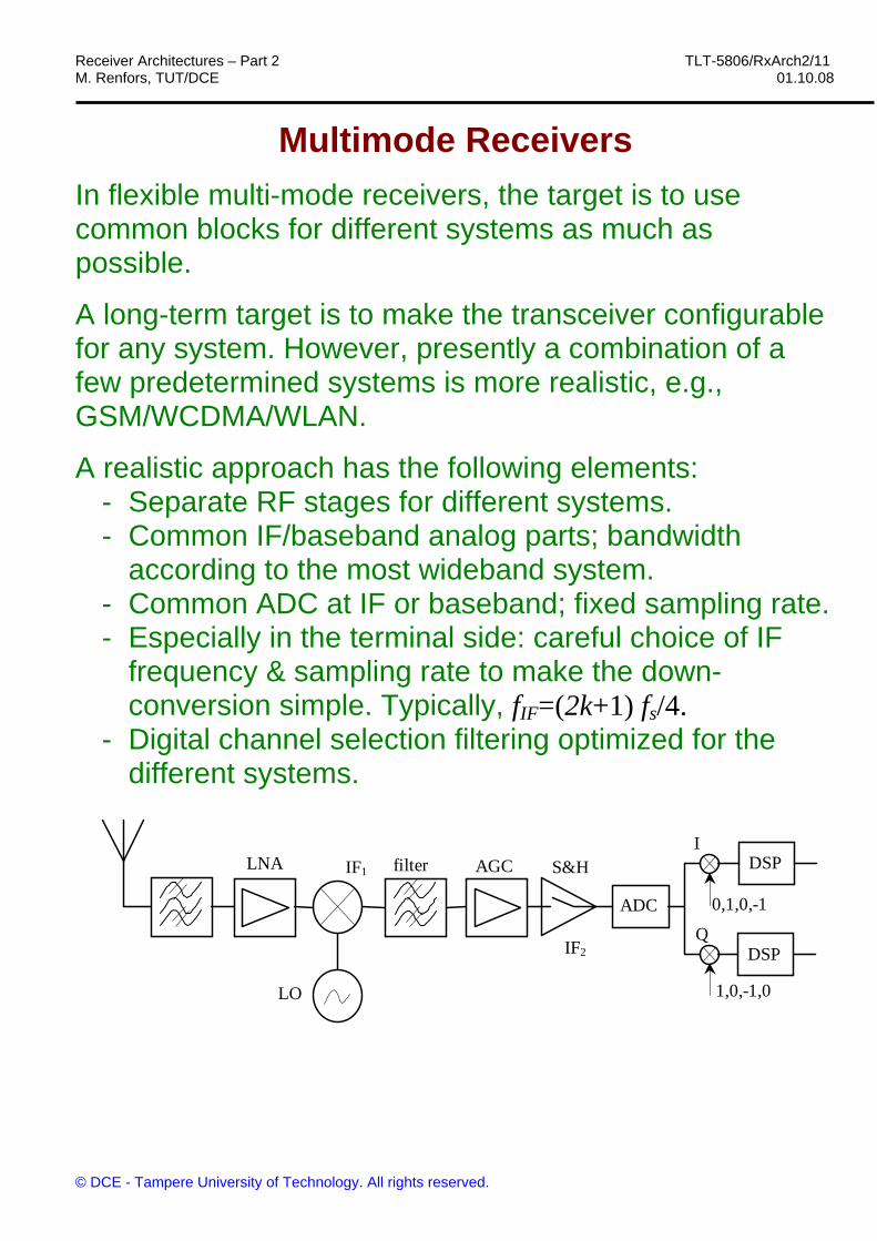
Multimode Receivers In flexible multi-mode receivers, the target is to use common blocks for different systems as much as possible.
A long-term target is to make the transceiver configurable for any system. However, presently a combination of a few predetermined systems is more realistic, e.g., GSM/WCDMA/WLAN.
A realistic approach has the following elements: - Separate RF stages for different systems. - Common IF/baseband analog parts; bandwidth
according to the most wideband system. - Common ADC at IF or baseband; fixed sampling rate. - Especially in the terminal side: careful choice of IF
frequency & sampling rate to make the down-conversion simple. Typically, fIF=(2k+1) fs/4.
- Digital channel selection filtering optimized for the different systems.
Common features for 1-3: • Analog & A/D bandwidth according to the widest
channel bandwidth Common features for 4 and 5: • Tunable digital channel selection and down-conversion • Interesting mostly for base-station applications
Receiver Architectures – Part 2 TLT-5806/RxArch2/13 M. Renfors, TUT/DCE 01.10.08
1. Multimode direct-conversion receiver Strengths - Simple analog part - Sampling jitter not critical - Narrowband A/D-conversion can be used Weaknesses - DC-offset problems, especially difficult to handle in
flexible receiver - 2nd-order intermodulation -> bigger demands for the
linearity of the analog parts Oportunities - Fast and flexible DC-offset compensation techniques,
facilitated by high resolution A/D-conversion techniques.
Receiver Architectures – Part 2 TLT-5806/RxArch2/14 M. Renfors, TUT/DCE 01.10.08
2. Multimode low IF receiver Strengths - Rather simple analog part - Sampling jitter not critical - Narrowband A/D-conversion can be used - DC-problems avoided Weaknesses - 2nd-order intermodulation -> bigger demands for the
linearity of the analog parts - Higher demands for I/Q balance - Multimode concept not very clear (different low-IF's for
different systems, or very hard demands for I/Q balance)
Oportunities - Adaptive I/Q imbalance compensation can be used to
loosen the requirements of the analog part.
Receiver Architectures – Part 2 TLT-5806/RxArch2/15 M. Renfors, TUT/DCE 01.10.08
possible - 2nd-order intermodulation not a problem - Narrowband A/D-conversion can be used - DC-problems avoided Weaknesses - Challenging demands for sampling jitter and linearity - IF filter difficult to integrate Oportunities - New technologies for flexible IF/RF filter implementation
(e.g., MEMS)
Receiver Architectures – Part 2 TLT-5806/RxArch2/16 M. Renfors, TUT/DCE 01.10.08
4. Wideband IF sampling architecture Strengths - Reduced IF filtering requirements - Simplified frequency synthesizer - Possibility to use common blocks for multiple channels - Facilitates fast frequency hopping/channel switching - DC-problems avoided Weaknesses - Very challenging demands for sampling jitter and
linearity - Wideband A/D-conversion needed - 2nd-order intermodulation may be a problem - Lot of DSP power needed - High power consumption Oportunities - Advances in ADC technologies and DSP HW
Receiver Architectures – Part 2 TLT-5806/RxArch2/17 M. Renfors, TUT/DCE 01.10.08
5. Wideband direct-conversion/low-IF architecture Strengths - Simplified frequency synthesizer - Possibility to use common blocks for multiple channels - Facilitates fast frequency hopping/channel switching - Rather simple analog part - Sampling jitter not critical Weaknesses - Hard demands for I/Q balance - Multimode concept not very clear (avoiding DC-offset
problems in all different systems) - Wideband A/D-conversion needed - 2nd-order intermodulation -> bigger demands for the
linearity of the analog parts - High power consumption Oportunities - Adaptive I/Q imbalance compensation can be used to
loosen the requirements of the analog part.
Receiver Architectures – Part 2 TLT-5806/RxArch2/18 M. Renfors, TUT/DCE 01.10.08
6. Direct-sampling receiver Strengths - Simplest possible analog part - Highly flexible for multi-standard receivers. Weaknesses - Very hard jitter requirements. - Currently not feasible for demanding system specs or
high-order modulation. Oportunities - Novel ideas for sampling and ADCs - Analog discrete-time processing techniques.
Receiver Architectures – Part 2 TLT-5806/RxArch2/19 M. Renfors, TUT/DCE 01.10.08
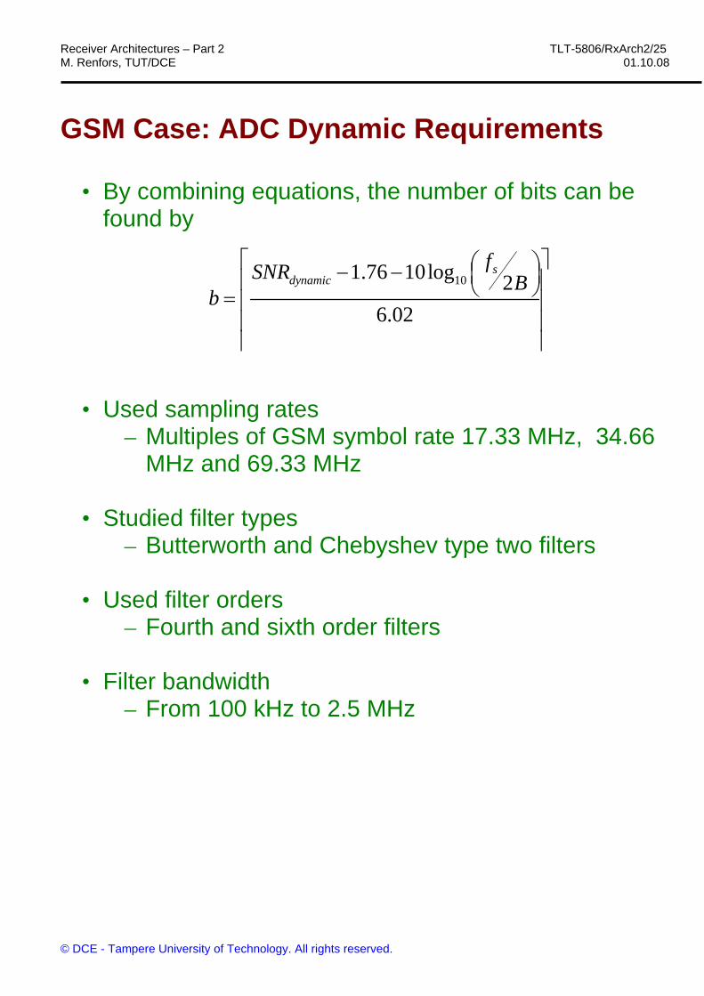
14AD−conventers Bits as a Function of Filter Bandwidth. Fs = 92.16MHz
500 1000 1500 2000 2500 3000 3500 4000 4500 5000
2
4
6
8
10
12
14
Bits
use
d in
AD
−co
nver
ter
AD−conventers Bits as a Function of Filter Bandwidth. Fs = 69.333MHz
500 1000 1500 2000 2500 3000 3500 4000 4500 5000
2
4
6
8
10
12
14
Filters bandwidth [kHz]
AD−conventers Bits as a Function of Filter Bandwidth. Fs = 34.6666MHz
Sixth-order Chebyshev type two filters:
Notice that in practice the minimum number of bits is higher than the lowest values indicated here, in order to be able to carry out the channel equalization properly.
500 1000 1500 2000 2500 3000 3500 4000 4500 5000
2
4
6
8
10
12
14AD−conventers Bits as a Function of Filter Bandwidth. Fs = 92.16MHz
500 1000 1500 2000 2500 3000 3500 4000 4500 5000
2
4
6
8
10
12
14
Bits
use
d in
AD
−co
nver
ter
AD−conventers Bits as a Function of Filter Bandwidth. Fs = 69.333MHz
500 1000 1500 2000 2500 3000 3500 4000 4500 5000
2
4
6
8
10
12
14
Filters bandwidth [kHz]
AD−conventers Bits as a Function of Filter Bandwidth. Fs = 34.6666MHz
Receiver Architectures – Part 2 TLT-5806/RxArch2/27 M. Renfors, TUT/DCE 01.10.08
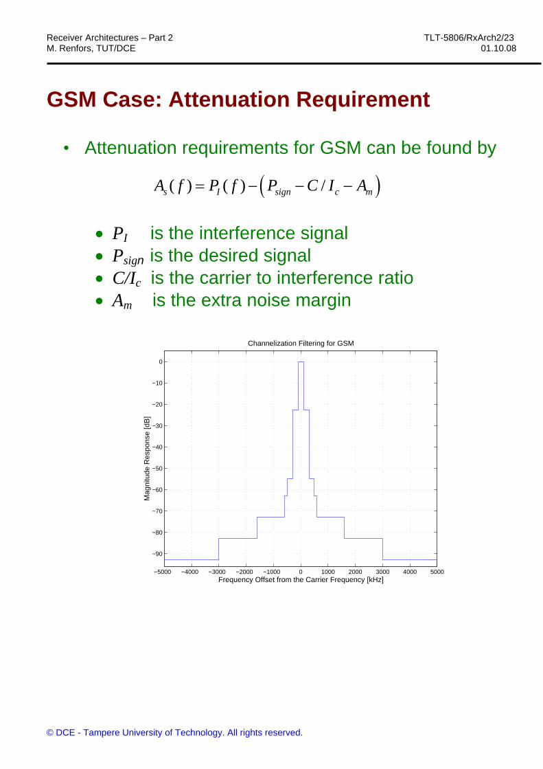
GSM Case: Jitter Noise The maximum signal power to be sampled is:
( ) ( ){ }maxADC IfP P f H f= +
Using the standard white-noise model for the jitter effects, the maximum allowed standard deviation of the timing error is given by:
In advanced SW radio concepts, the selectivity filtering and down-conversion are moved from analog continuous-time part to the discrete-time/DSP part. => Here efficient multirate filtering techniques become very important. It also helps to move as much as possible functionality from the analog or digital front-end to baseband processing. => All-digital synchronization concept becomes very interesting in this context. Some errors due to RF-front-end can be corrected by DSP. Example: Adaptive I/Q imbalance compensation.
Receiver Architectures – Part 2 TLT-5806/RxArch2/32 M. Renfors, TUT/DCE 01.10.08
Digital Channel Selection & Down-Conversion Digital Down-Conversion 1. Desired channel centered at fixed IF
=> Fixed down-conversion Special choices of fIF and fs make things easy. Especially when fIF=(2k+1) fs/4, the signal aliases to fs/4 and down-conversion is very easy.
2. Wideband sampling case => Tunable down-conversion and NCO (numerically controlled oscillator) needed.
3. Stepwise mixing and decimation => Tunable digital down-conversion is possible also without NCO, as demonstrated in the later example. However, it is not easy to find sufficiently efficient and flexible schemes.
Channel Selection Filtering - After down-conversion, efficient lowpass decimator structure
is needed. - CIC-filters are commonly used in the first decimation stages,
FIR-filters and the last stages. Nth-band IIR filters also an efficient solution.
Adjusting Symbol Rates - Different systems use different symbol/chip rates. - Common sampling clock frequency is preferred.
=> Decimaton by a fractional factor is needed. - This can be done at baseband or earlier in the decimation
chain.
Receiver Architectures – Part 2 TLT-5806/RxArch2/35 M. Renfors, TUT/DCE 01.10.08
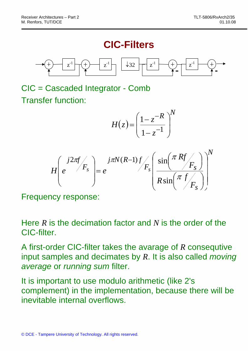
CIC = Cascaded Integrator - Comb Transfer function:
Frequency response: Here R is the decimation factor and N is the order of the CIC-filter.
A first-order CIC-filter takes the avarage of R consequtive input samples and decimates by R. It is also called moving average or running sum filter.
It is important to use modulo arithmetic (like 2's complement) in the implementation, because there will be inevitable internal overflows.
z-1 z-1z-1 z-1
( )NR
zzzH ⎟
⎟⎠
⎞⎜⎜⎝
⎛
−
−=
−
−
111
N
s
sFfRNj
Ffj
FfR
FRf
eeH ss
⎟⎟⎟⎟
⎠
⎞
⎜⎜⎜⎜
⎝
⎛
⎟⎠⎞⎜
⎝⎛
⎟⎠⎞⎜
⎝⎛
=⎟⎟⎟
⎠
⎞
⎜⎜⎜
⎝
⎛ −
π
πππ
sin
sin)1(2
Receiver Architectures – Part 2 TLT-5806/RxArch2/36 M. Renfors, TUT/DCE 01.10.08
CIC-Filters In CIC filter, those frequencies aliasing to 0-frequency are heavily attenuated. For a relatively narrowband signal, low-order CIC-filters are sufficient; more wideband signals neede higher CIC-filter orders Example (for a GSM application): N=2, R=32.
Receiver Architectures – Part 2 TLT-5806/RxArch2/37 M. Renfors, TUT/DCE 01.10.08
NCO-Based Arbitrary Digital Down-Conversion
Dedicated processors implementing the following kind of down-conversion and channel selection structure are available for several vendors (like Harris).
Sampling rates in the 50 ... 100 MHz range are possible. However, the power consumption is still too high for terminal applications.
Stepwise Decimation and Mixing Approach With suitable choice of the key parameters (IF frequency, channel spacing, sampling rate) it is possible to do adjustable down-conversion also without NCO, just by using the frequency translations of multirate DSP. In the following, a special bandpass decimator structure is described, which gives some more flexibility in this kind of solutions. The idea is to do stepwise down-conversion, with decimation by 2 in each stage. Three different types of stages are used:
1. Lowpass decimation when the desired signal is at the lower frequencies.
2. Highpass decimation when the desired signal is at the higher frequencies.
3. The special bandpass decimator when the desired signal is in the mid-frequencies.
Note: This example should be taken as an example of the possibilities of complex signal processing in specific designs, but not as a generic technique for SDR.
Receiver Architectures – Part 2 TLT-5806/RxArch2/41 M. Renfors, TUT/DCE 01.10.08
Bandpass Decimator
The structure includes: - down-conversion by fs/8 - bandpass filtering - decimation by 2 Complex filtering is needed in the basic model, but the structure can be optimized to an efficient form, where complex signal processing is not needed. Basic model:
Receiver Architectures – Part 2 TLT-5806/RxArch2/42 M. Renfors, TUT/DCE 01.10.08
Bandpass Decimator (continued) Optimized form:
A1(z)
A0(z)
A3(z)
A2(z)
+
+x
1,1,-1,-1,1,1,-1
-
-
- This is completely equivalent to the original form. - No complex signal processing actually needed. - All filtering operations running at quarter of the sampling
rate. - Computational complexity roughly the same as for half-