Recipes for MPC574xGSoftware examples and startup code to exercise microcontroller featuresby: Steve Mihalik, Jose Cisneros, Rebeca Delgado, Diego Haro, Arturo Inzuza, Scott Obrien, Hugo Osornio, Murray Stewart
1 IntroductionThis document provides software examples and describes necessary startup steps taken to help users get started with the MPC574xG MCU.
Complete source code and projects are available in a separate zip file at freescale.com. Projects are implemented using Green Hills Software (GHS) compiler version 2013.5.4 or later on MPC5748G.
Code shown in this application note is for MPC5748G Rev. 1, but the source code on line has versions for both MPC5748G Rev. 0 and Rev. 1.
Basic software characteristics of examples:
• One core (core 0) is started after reset
• Core 0 performs general initializations such asclocks and then starts other cores
• All cores execute from one output file (ELF file)
• New sub-projects can be created using one of theother sub-projects as a starting point.
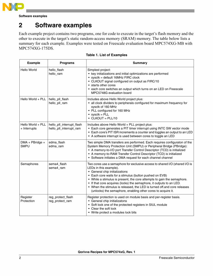
2 Software examplesEach example project contains two programs, one for code to execute in the target’s flash memory and the other to execute in the target’s static random-access memory (SRAM) memory. The table below lists a summary for each example. Examples were tested on Freescale evaluation board MPC574XG-MB with MPC574XG-175DS.
Table 1. List of Examples
Example Programs Summary
Hello World hello_flashhello_ram
Simplest project: • key initializations and initial optimizations are performed • sysclk = default 16MHz FIRC clock • CLKOUT signal configured on output as FIRC/10 • starts other cores • each core switches an output which turns on an LED on Freescale
MPC5748G evaluation board
Hello World + PLL hello_pll_flashhello_pll_ram
Includes above Hello World project plus: • all clock dividers to peripherals configured for maximum frequency for
sysclk of 160 MHz • PLL configured for 160 MHz • sysclk = PLL • CLKOUT = PLL/10
Hello World + PLL + Interrupts
hello_pll_interrupt_flashhello_pll_interrupt_ram
Includes above Hello World + PLL project plus: • Each core generates a PIT timer interrupt using INTC SW vector mode • Each core’s PIT ISR increments a counter and toggles an output to an LED • A software interrupt is used between cores to toggle an LED
DMA + PBridge + SMPU
edma_flashedma_ram
Two simple DMA transfers are performed. Each requires configuraton of the System Memory Protection Unit (SMPU) or Peripheral Bridge (PBridge): • A memory-to-I/O port Transfer Control Descriptor (TCD) is initialized • A memory-to-RAM Transfer Control Descriptor (TCD) is initialized • Software initiates a DMA request for each channel channel
Semaphores sema4_flashsema4_ram
Two cores use a semaphore for exclusive access to shared I/O (shared I/O is LEDs in this example). • General chip initializations • Each core waits for a stimulus (button pushed on EVB) • While a stimulus is present, the core attempts to gain the semaphore. • If that core acquires (locks) the semaphore, it outputs to an LED. • When the stimulus is released, the LED is turned off.and core releases
(unlocks) the semaphore, enabling other cores to acquire it.
Register Protection
reg_protect_flashreg_protect_ram
Register protection is used on module basis and per-register basis. • General chip initializatons • Soft lock one of the protected registers in SIUL module • Clear the soft lock • Write protect a modules lock bits
Qorivva Recipes for MPC574xG, Rev. 1
Freescale Semiconductor2
Software examples
Low Power - STOP lp_stop_flashlp_stop_ram
Enter and exit STOP mode based on RTC values. Program runs continous loop of: • Toggle output to LED on Freescale evaluation board • Configure RTC value • Clear any prior RTC wakeup flag • Enter STOP mode • On STOP mode exit, verify correct mode
Analog-to Digital Converter
adc_flashadc_ram
ADC module read inputs using normal scan, continuous mode: • General chip initializatons • Configures pads for analog input and selects ADC channels • ADC calibration • ADC initialization for normal scan • Reads analog input • On a Freescale EVB, one analog input is a pot connected to VDD. The
voltage read is output to four LEDs as a scaled binary number.
Timed I/O emios_flashemios_ram
eMIOS module is used to create timed I/O functions including: • General chip initializations • Modulus Conter Buffered (MCB) • Output Pulse Width Modulation Buffered (OPWMB) • Output Pulse Width and Frequency Modulation Buffered (OPWFMB) • Input Period Measurement (IPM) • Input Pulse Width Measurement (IPWM)
CAN flexcan_flashflexcan_ram
FlexCAN modules are used to transmit and receive a single CAN 2.0 B message: • General chip initializations • Initialize two FlexCAN modules • Transmit message received by other module
LIN linflexd_lin_flashlinflexd_lin_ram
LINFlexD: Transmit and receive LIN messages • General chip initializations • Initialize LINFlexD_1 as master at 10.417K baud • Loop: Master transmits frame, Master transmits header for slave
information
UART linflexd_uart_flashlinflexd_uart_ram
LINFlexD module transmits and recieves characters one byte at a time: • General chip initializations • Initialize LINFlexD_2 module • Transmit an initial string of characters • Loop: Receive a byte then echo it back
SPI spi_flashspi_ram
SPI to SPI transfers initiated by software • General chip initializations • Initialize DSPI 3 as master and SPI 1 as slave and their pads • Loop: Write slave response data, write master transmit data, read results
SPI+ DMA spi_dma_flashspi_dma_ram
SPI to SPI transfers initiated by DMA requests • General chip initializations • Configure PBridge to enable DMA to SPI and high priority DMA at crossbar • Configure eDMA and DMA MUX to connect eDMA to DSPI_3 and SPI_1 • Initialize DSPI 3 and SPI 1 modules and their pads • Start high speed SPI transfers by enabling eDMA channels for SPI
Table 1. List of Examples
Example Programs Summary
Qorivva Recipes for MPC574xG, Rev. 1
Freescale Semiconductor 3
Software examples
2.1 Hello worldDescription: This short project is a starting point to learn basic initialization. The project boots from core 0, the default boot core for MPC5748G. Core 0 performs key initializations and initial optimizations before starting other cores. All cores switch to an output pin low.
Design Summary:
• Boot core 0 per BAF configuration in flash
• Perform key initializations before main:
— Initialize all platform SRAM
— Initialize instruction and data caches
— Enable core’s branch target buffers for faster execution of branch instructions
memory_config_16mhz(); /* Configure wait states, flash master access, etc. */ crossbar_config(); /* Configure crossbar */ /* (Example does not require peripheral clock gating)*/ __ghs_board_devices_init_AFTER_main(); /* Start core 1 & core 2 */ /* __ghs_board_devices_init_AFTER_main does the folowing for cores 1 & 2 : From Core 0 (current core): configures & starts cores 1 & 2 by: 1. Verifies core is not already running. If it is it returns. 2. MC_ME_CCTL[n]: enables all RUN modes for that core 3. MC_ME.CADDR[n]: loads address __ghs_mpc5748g_cpu[n]_entry 4. MC_ME.CADDR[n]: sets RMC bit to reset core on mode change. 5. Mode transition to DRUN to activate core (RMC clears on mode change) From Cores 1 and 2: runs __ghs_mpc5748g_cpu[n]_entry which: 1. branches to __ghs_e200z4204_core_init which: 2. sets MSR[ME]=1 3. sets IVPR = 0x4000_0000 4. initilizes data & instruction caches if they exist 5. initializes unique sp but common sda & sda2 6. if main_core1 exists, branches to it else branches to self */
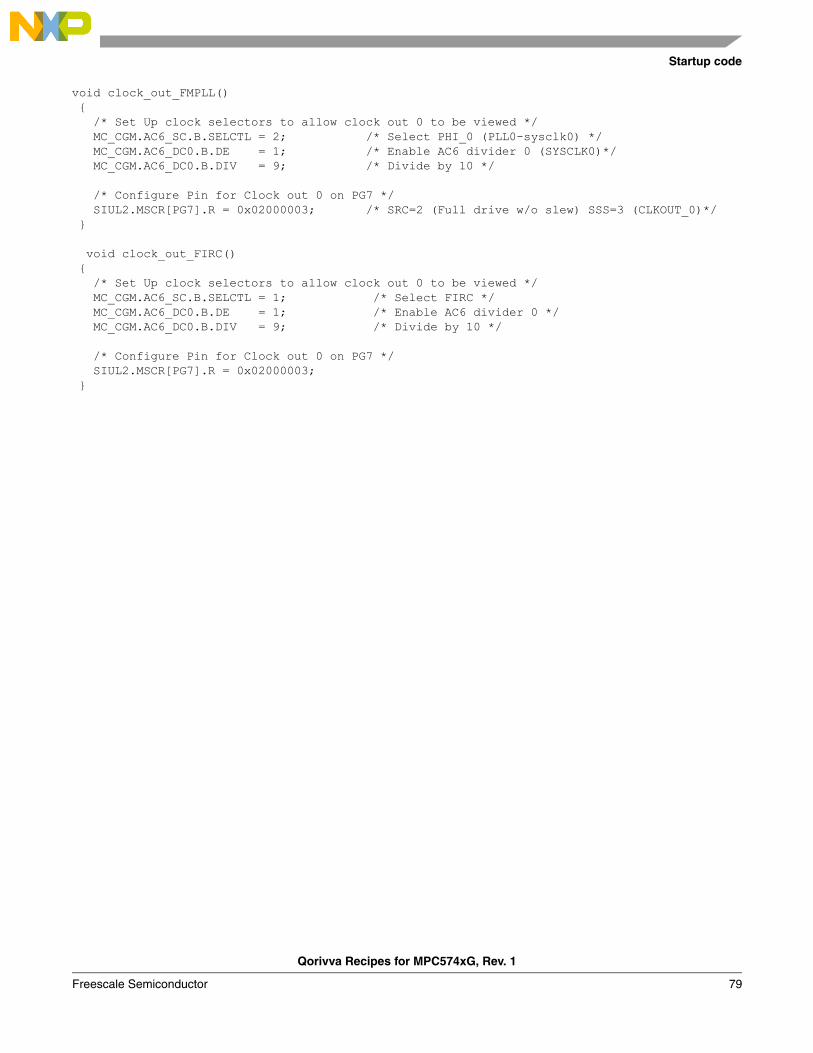
SIUL2.MSCR[PG2].B.OBE = 1; /* Pad PG2 (98): OBE=1. On EVB active low LED1 */ clock_out_FIRC(); /* Pad PG7 = CLOCKOUT = FIRC / 10 */ while(1) { i++; }}
Qorivva Recipes for MPC574xG, Rev. 1
Freescale Semiconductor 5
Software examples
2.1.2 main_core_1.cmain_core_1(){ uint32_t j = 0;
SIUL2.MSCR[PG3].B.OBE = 1; /* Pad PG3 (99) OBE=1. On EVB active low LED2 */ while(1){ j++; }}
2.1.3 main_core_2.cmain_core_2(){ uint32_t k = 0;
SIUL2.MSCR[PG4].B.OBE = 1; /* Pad PG4 (100) OBE=1. On EVB active low LED3 */ while(1){ k++; }}
Qorivva Recipes for MPC574xG, Rev. 1
Freescale Semiconductor6
Software examples
2.2 Hello world + PLLDescription: This project expands the prior hello world project by additional configurations to start and use the PLL at 160 MHz for the system clock.
Design Summary:
• Perform prior hello project sequence but do not start other cores yet
• Initialize clock dividers to peripherals for their maximum frequency based on 160 MHz clock
• Configure PLL for 160 MHz based on 40 MHz crystal input
*/ SIUL2.MSCR[PG2].B.OBE = 1; /* Pad PG2 (98): OBE=1. On EVB active low LED1 */ clock_out_FMPLL(); /* Pad PG7 = CLOCKOUT = PLL0/10 */ __ghs_board_devices_init_AFTER_main(); /* start cores 1 & 2 */ /* __ghs_board_devices_init_AFTER_main does the folowing for cores 1 & 2 : From Core 0 (current core): configures & starts cores 1 & 2 by: 1. Verifies core is not already running. If it is it returns. 2. MCME_CCTL[n]: enables all RUN modes for that core 3. MC_ME.CADDR[n]: loads address __ghs_mpc5748g_cpu[n]_entry 4. MC_ME.CADDR[n]: sets RMC bit to reset core on mode change. 5. Mode transition to DRUN to activate core (RMC cleared on mode change) From Cores 1 and 2: runs __ghs_mpc5748g_cpu[n]_entry which: 1. branches to __ghs_e200z4204_core_init which: 2. sets MSR[ME]=1 3. sets IVPR = 0x4000_0000 4. initilizes data & instruction caches if they exist 5. initializes unique sp but common sda & sda2 6. if main_core1 exists, branches to it else branches to self */ while(1) { i++; }}
2.2.2 main_core_1.cmain_core_1(){ uint32_t j = 0;
SWT_disable_1(); /* Disable watchdog for core 1 */ SIUL2.MSCR[PG3].B.OBE = 1; /* Pad PG3 (99) OBE=1. On EVB active low LED2 */ while(1){ j++; }}
2.2.3 mainc_core_2.cmain_core_2(){ uint32_t k = 0;
SWT_disable_2(); /* Disable watchdog for core 2 */ SIUL2.MSCR[PG4].B.OBE = 1; /* Pad PG4 (100) OBE=1. On EVB active low LED3 */ while(1){ k++; }}
Qorivva Recipes for MPC574xG, Rev. 1
Freescale Semiconductor8
Software examples
2.3 Hello world + PLL + InterruptsDescription: Expanding the prior hello_pll project, here each core generates a PIT timer interrupt that is serviced by core. The PIT interrupt service routines toggle the output connected to LEDs on Freescale evaluation boards. The PIT counts at a rate of sysclk/4. The PIT timers count down from an initial load value and generate an interrupt request when they reach zero. The table below summaries the program behaviour.
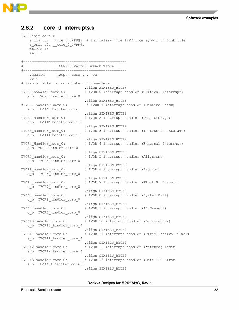
Each core has it’s own Interrupt Vector Prefix Register (spr IVPR) which provides the upper address bits for interrupts for that core. IVPR is different for each core, so each core has a unique branch table for core interrupts in this example.
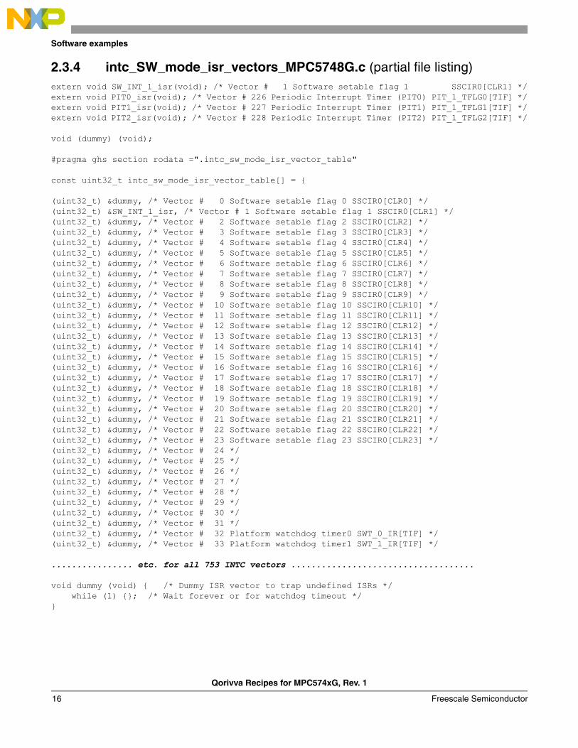
The interrupt controller (INTC) is configured for software vector mode for all cores. All cores use the same base for the INTC ISR vector table. Interrupt requests to the INTC can be routed to any core or even multiple cores. Generally, a peripheral will only send an interrupt request to one core.
Table 6. hello_pll_interrupt program behaviour
LED ISR Controlling LED Core Executing Toggle Period
tgt\libboardinit mpc5748g_rev_core0_only.ppc 27 Jan 2015
Qorivva Recipes for MPC574xG, Rev. 1
Freescale Semiconductor 9
Software examples
Design Summary:
Core 0 (boot core) reset to end of main:
• Perform general project sequence in the prior hello_pll project, but do not starting other cores yet
• Configure sysclk as PLL at 160 MHz based on 40 MHz crystal input
— Includes configuring clock dividers to peripherals for their maximum frequencies based on 160 MHz sysclk. (PIT clock is initialized to sysclk/4 = 40 MHz)
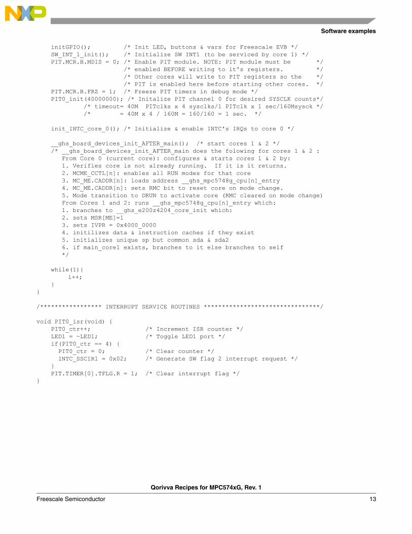
/************************************ Main ***********************************/void main(){ uint32_t i = 0;
memory_config_160mhz(); /* Config. wait states, flash master access, etc*/ crossbar_config(); /* Configure crossbar */ peri_clock_gating(); /* Config gating/enabling peri. clocks for modes*/ /* Configuraiton occurs after mode transition! */ system160mhz(); /* Sets clock dividers= max freq, calls PLL_160MHz function which: MC_ME.ME: enables all modes for Mode Entry module Connects XOSC to PLL PLLDIG: LOLIE=1, PLLCAL3=0x09C3_C000, no sigma delta, 160MHz MC_ME.DRUN_MC: configures sysclk = PLL Mode transition: re-enters DRUN which activates PLL=sysclk & peri clks */
Qorivva Recipes for MPC574xG, Rev. 1
Freescale Semiconductor12
Software examples
initGPIO(); /* Init LED, buttons & vars for Freescale EVB */ SW_INT_1_init(); /* Initialize SW INT1 (to be serviced by core 1) */ PIT.MCR.B.MDIS = 0; /* Enable PIT module. NOTE: PIT module must be */ /* enabled BEFORE writing to it's registers. */ /* Other cores will write to PIT registers so the */ /* PIT is enabled here before starting other cores. */ PIT.MCR.B.FRZ = 1; /* Freeze PIT timers in debug mode */ PIT0_init(40000000); /* Initalize PIT channel 0 for desired SYSCLK counts*/ /* timeout= 40M PITclks x 4 sysclks/1 PITclk x 1 sec/160Msysck */ /* = 40M x 4 / 160M = 160/160 = 1 sec. */
init_INTC_core_0(); /* Initialize & enable INTC's IRQs to core 0 */ __ghs_board_devices_init_AFTER_main(); /* start cores 1 & 2 */ /* __ghs_board_devices_init_AFTER_main does the folowing for cores 1 & 2 : From Core 0 (current core): configures & starts cores 1 & 2 by: 1. Verifies core is not already running. If it is it returns. 2. MCME_CCTL[n]: enables all RUN modes for that core 3. MC_ME.CADDR[n]: loads address __ghs_mpc5748g_cpu[n]_entry 4. MC_ME.CADDR[n]: sets RMC bit to reset core on mode change. 5. Mode transition to DRUN to activate core (RMC cleared on mode change) From Cores 1 and 2: runs __ghs_mpc5748g_cpu[n]_entry which: 1. branches to __ghs_e200z4204_core_init which: 2. sets MSR[ME]=1 3. sets IVPR = 0x4000_0000 4. initilizes data & instruction caches if they exist 5. initializes unique sp but common sda & sda2 6. if main_core1 exists, branches to it else branches to self */ while(1){
i++; }}
/***************** INTERRUPT SERVICE ROUTINES ********************************/
.align 4 IVOR4_Handler_core_0: prologue_core_0: e_stwu r1,-0x50 (r1) # Create stack frame and store back chain e_stmvsrrw 0x0c (r1) # Save SRR[0-1] (must be done before enabling MSR[EE]) se_stw r3, 0x08 (r1) # Save working register (r3) e_lis r3, INTC_IACKR0@ha # Save address of INTC_IACKR0 in r3 se_lwz r3, INTC_IACKR0@l(r3) # Save contents of INTC_IACKR0 in r3 (vector table address) wrteei 1 # Set MSR[EE] (must wait a couple clocks after reading IACKR) se_lwz r3, 0x0(r3) # Read ISR address from Interrupt Vector Table using pointer e_stmvsprw 0x14 (r1) # Save CR, LR, CTR, XER se_mtLR r3 # Copy ISR address (from IACKR) to LR for next branch e_stmvgprw 0x24 (r1) # Save GPRs, r[0,3-12] se_blrl # Branch to ISR, with return to next instruction (epilogue)
epilogue_core_0: e_lmvsprw 0x14 (r1) # Restore CR, LR, CTR, XER e_lmvgprw 0x24 (r1) # Restore GPRs, r[0,3-12] e_lis r3, INTC_EOIR0@ha # Load upper half of INTC_EOIR0 address to r3 mbar # Ensure prior clearing of interrupt flag conmpleted. wrteei 0 # Disable interrupts se_stw r3, INTC_EOIR0@l(r3) # Load lower half of INTC_EOIR0 address to r3 and # write contents of r3 to INTC_EOIR0 se_lwz r3, 0x08 (r1) # Restore working register (r3) (original value) e_lmvsrrw 0x0c (r1) # Restore SRR[0-1] e_add16i r1, r1, 0x50 # Reclaim stack space se_rfi # End of Interrupt Handler - re-enables interrupts
Qorivva Recipes for MPC574xG, Rev. 1
Freescale Semiconductor 17
Software examples
2.3.6 cores_0-2_interrupt_vectors.s (partial listing for core 0 code subset)
................... etc. for up to IVOR15 and other cores ..................................
Qorivva Recipes for MPC574xG, Rev. 1
Freescale Semiconductor18
Software examples
2.4 DMA + PBridge + SMPUDescription: Two DMA transfers are performed using separate Transfer Control Descriptors (TCDs):
• Memory to memory
— A string of bytes is transferred from memory to SRAM memory.
— Cache coherency must be addressed because core data caches are enabled and eDMA writes to data memory without the knowledge of the core caches.
— The System Memory Protection Unit (SMPU) will be configured to include one memory region which will bypasses cache (“cache inhibited”). This ensures cores read (and write) directly from RAM rather than cache for the shared RAM region.
• Memory to peripheral
— A string of bytes is written to a GPIO output port. On a Freescale EVB the port is connected to an LED.
— Peripheral Bridge (PBridge) default configuration must be changed to allow eDMA to access the desired peripheral.
Both examples use software to initiate the transfer instead of a peripheral’s DMA request hardware. The intent is to get users familiar with eDMA terms and operations. Stepping through code in the transfer loop allows viewing TCD changes with a debugger.
The TCD describes the channel’s transfer. Each channel has a structure shown in the figure below. At reset, the fields are cleared on MPC574xG. The DMA multiplexer is not needed here, hence not initialized.
Only one byte of data will be transferred with each DMA service request. Hence the “minor loop” is simply one transfer, which transfers one byte. The “major loop” here consists of 12 minor loop iterations.
Because a peripheral is not involved in this example, automatic DMA handshaking will not occur. Instead, the software handshaking given here must be implemented for each transfer:
• Start DMA service request (set a START bit).
• Poll when that request is done (check the CITER bit field).
These steps appear “messy” for every transfer, which is only a byte in this example. However, remember that when using actual peripherals, software never has to do these steps; they are done automatically by hardware. The purpose of this example is to illustrate how to set up a DMA transfer.
Qorivva Recipes for MPC574xG, Rev. 1
Freescale Semiconductor 19
Software examples
Figure 1. eDMA Transfer Control Descriptor (TCD) Structure1
The START bit is normally set by the peripheral requesting service. Once the DMA processing engine activates the channel, the ACTIVE bit is set. (If the DMA engine was busy servicing other channels, one could cancel the transfer by clearing the START bit. The ACTIVE bit would then need to be checked to ensure service did not start on that channel.
PBridge. By reset default, MPC5648G’s eDMA does not have read or write access to any peripheral! This is the default configuration of PBRIDGE A and PBRIDGE B. This can be changed in registers Master Privilege Register A and Master Privilege Regsiter B of modules AIPSx_MPRA and AIPSxMPRB. See table below for mapping of masters.
1.MPC5748G Reference Manual, Rev 3, page 3358
Qorivva Recipes for MPC574xG, Rev. 1
Freescale Semiconductor20
Software examples
SMPU. Cache coherency is an issue when there are multiple masters sharing data. In this example the first DMA writes to SRAM. The core, and hence JTAG debugger, may read the variable and it will automatically go into its data cache. Subsequent reads of the array will not contain any updates to the array in SRAM done by DMA.
The solution implmented here is to cache inhibit the arrray writtin to by DMA. This is done by the SMPU. Simply two memory regions are defined: one for all of SRAM, the other for a subset within the first SRAM region. The smaller subset is for data written by DMA. This second region will have the Cache Inhibit (CI) attribute = 1. SMPU attributes are OR’d together where regions overlap, so just that variable is cache inhibited. Minimum regions size is 16 bytes, as used here.
Table 9. MPC5748G Mapping of Masters #s to Crossbars and PBridges
MasterCrossbar Physical Master #
(AXBS_0)Crossbar Physical Master #
(AXBS_1)PBridges Logical
Master #
e200z4a - Instruction 0 0
e200z4a - data 1 0
e200z4b - Instruction 2 1
e200z4b - data 3 1
e200z2 - Instruction 4 2
e200z2 - data 5 2
eDMA 6 4
HSM 7 3
AXBS_0 - slave 3 0 -
AXBS_0 - slave 4 1 -
Ethernet 2 5
FlexRay 3 6
MLB 4 7
USB_0 5 11
USB_1 6 12
SDHC 7 13
Qorivva Recipes for MPC574xG, Rev. 1
Freescale Semiconductor 21
Software examples
Design Summary:
• Perform general chip initializations such as in previous hello world projects including:
— setting sysclk to 160 MHC PLL
— enabling a port as output, which is connected to LED 1on Freescale EVBs
— adding read/write ability for other master besides cores (like eDMA)
tgt\libboardinit mpc5748g_rev_core0_only.ppc 27 Jan 2015
Table 11. I/O Connections: DMA + PBridge + SMPU program
Port Signal SIUL_MSCR # Comment
PG2 GPIO output 98 Connected to LED 1 on Freescale evalutaion board using default jumpers.
Qorivva Recipes for MPC574xG, Rev. 1
Freescale Semiconductor22
Software examples
2.4.1 main_core_0.c/*****************************************************************************//* bridges_config *//* Description: Configures bridges to provide desired RWX and user/supervisor*//* access and priorites by crossbar masters to crossbar slaves. *//*****************************************************************************/
void bridges_config (void) { AIPS_A.MPRA.R |= 0x00007000; /* Enable DMA RWU for PBRIDGE A */}
/************************************ Main ***********************************/
memory_config_160mhz(); /* Configure wait states, flash master access, etc.*/ crossbar_config(); /* Configure crossbar */ bridges_config(); /* Enable R/W to peripherals by DMA & all masters*/ smpu_config(); /* Cache inhibit a RAM region for shared data */ system160mhz(); /* sysclk=160MHz, dividers configured, mode trans*/
SIUL2.GPDO[PG2].R = 1; /* Pad PG2 (98): Output=1 (EVB's LED1 off) */ SIUL2.MSCR[PG2].B.OBE = 1; /* Pad PG2 (98): Enable output to pad */
init_edma_channel_arbitration(); /* Initialze arbitration among channels */ initTCDs(); /* Initialize DMA Transfer Control Descriptors */
EDMA.SERQ.R = 0; /* Enable EDMA channel 0 */ /* Initiate DMA service using software activation: */
EDMA.SSRT.R = 0; /* Set chan 0 START bit to initiate 1st minor loop */ while (EDMA.TCD[0].CITER.ELINKNO.B.CITER != 1) { /* while CITER != 1 (not on last minor loop), */ /* wait for START=0 and ACTIVE=0 */ while ((EDMA.TCD[0].CSR.B.START == 1) | (EDMA.TCD[0].CSR.B.ACTIVE == 1)) {} EDMA.SSRT.R = 0; /* Set chan 0 START bit again for next minor loop */ }
EDMA.SSRT.R = 1; /* Set chan 1 START bit to initiate 1st minor loop */ while (EDMA.TCD[1].CITER.ELINKNO.B.CITER != 1) { /* while CITER != 1 (not on last minor loop), */ /* wait for START=0 and ACTIVE=0 */ while ((EDMA.TCD[1].CSR.B.START == 1) | (EDMA.TCD[1].CSR.B.ACTIVE == 1)) {} EDMA.SSRT.R = 1; /* Set chan 0 START bit again for next minor loop */ } while (1) {i++;}}
void initTCDs(void) { /* Transfer string to port pin output */
EDMA.TCD[0].SADDR.R = (vuint32_t) &TCD0_SourceData; /* Load source address*/ EDMA.TCD[0].ATTR.B.SSIZE = 0; /* Read 2**0 = 1 byte per transfer */ EDMA.TCD[0].ATTR.B.SMOD = 0; /* Source modulo feature not used */ EDMA.TCD[0].SOFF.R = 1; /* After transfer add 1 to src addr*/ EDMA.TCD[0].SLAST.R = -12; /* After major loop, reset src addr*/
EDMA.TCD[0].DADDR.R = (vuint32_t) &TCD0_Destination ; /* Load dest. address*/ EDMA.TCD[0].ATTR.B.DSIZE = 0; /* Write 2**0 = 1 byte per transfer*/ EDMA.TCD[0].ATTR.B.DMOD = 0; /* Dest. modulo feature not used */ EDMA.TCD[0].DOFF.R = 1; /* After transfer add 1 to dst addr*/ EDMA.TCD[0].DLASTSGA.R = 0; /* After major loop no dest addr change*/ EDMA.TCD[0].NBYTES.MLNO.R = 1; /* Transfer 1 byte per minor loop */ EDMA.TCD[0].BITER.ELINKNO.B.ELINK = 0; /* No Enabling channel LINKing */ EDMA.TCD[0].BITER.ELINKNO.B.BITER = 13; /* 12 minor loop iterations */ EDMA.TCD[0].CITER.ELINKNO.B.ELINK = 0; /* No Enabling channel LINKing */ EDMA.TCD[0].CITER.ELINKNO.B.CITER = 13; /* Init. current iteraction count */
EDMA.TCD[0].CSR.B.DREQ = 1; /* Disable channel when major loop is done*/ EDMA.TCD[0].CSR.B.INTHALF = 0; /* No interrupt when major count half complete */ EDMA.TCD[0].CSR.B.INTMAJOR = 0; /* No interrupt when major count completes */ EDMA.TCD[0].CSR.B.MAJORELINK = 0; /* Dynamic program is not used */ EDMA.TCD[0].CSR.B.MAJORLINKCH = 0; /* No link channel # used */ EDMA.TCD[0].CSR.B.ESG = 0; /* Scatter Gather not Enabled */ EDMA.TCD[0].CSR.B.BWC = 0; /* Default bandwidth control- no stalls */ EDMA.TCD[0].CSR.B.START = 0; /* Initialize status flags START, DONE, ACTIVE */ EDMA.TCD[0].CSR.B.DONE = 0; EDMA.TCD[0].CSR.B.ACTIVE = 0;
EDMA.TCD[1].SADDR.R = (vuint32_t) &TCD1_SourceData; /* Load source address*/ EDMA.TCD[1].ATTR.B.SSIZE = 0; /* Read 2**0 = 1 byte per transfer */ EDMA.TCD[1].ATTR.B.SMOD = 0; /* Source modulo feature not used */ EDMA.TCD[1].SOFF.R = 1; /* After transfer add 1 to src addr*/ EDMA.TCD[1].SLAST.R = -12; /* After major loop, reset src addr*/
EDMA.TCD[1].DADDR.R = (vuint32_t) &SIUL2.GPDO[PG2].R ; /* Dest. addr. port 98*/ EDMA.TCD[1].ATTR.B.DSIZE = 0; /* Write 2**0 = 1 byte per transfer*/ EDMA.TCD[1].ATTR.B.DMOD = 0; /* Dest. modulo feature not used */ EDMA.TCD[1].DOFF.R = 0; /* After transfer add 1 to dst addr*/ EDMA.TCD[1].DLASTSGA.R = 0; /* After major loop no dest addr change*/ EDMA.TCD[1].NBYTES.MLNO.R = 1; /* Transfer 1 byte per minor loop */ EDMA.TCD[1].BITER.ELINKNO.B.ELINK = 0; /* No Enabling channel LINKing */ EDMA.TCD[1].BITER.ELINKNO.B.BITER = 12; /* 12 minor loop iterations */ EDMA.TCD[1].CITER.ELINKNO.B.ELINK = 0; /* No Enabling channel LINKing */
Qorivva Recipes for MPC574xG, Rev. 1
Freescale Semiconductor24
Software examples
EDMA.TCD[1].CITER.ELINKNO.B.CITER = 12; /* Init. current iteraction count */
EDMA.TCD[1].CSR.B.DREQ = 1; /* Disable channel when major loop is done*/ EDMA.TCD[1].CSR.B.INTHALF = 0; /* No interrupt when major count half complete */ EDMA.TCD[1].CSR.B.INTMAJOR = 0; /* No interrupt when major count completes */ EDMA.TCD[1].CSR.B.MAJORELINK = 0; /* Dynamic program is not used */ EDMA.TCD[1].CSR.B.MAJORLINKCH = 0; /* No link channel # used */ EDMA.TCD[1].CSR.B.ESG = 0; /* Scatter Gather not Enabled */ EDMA.TCD[1].CSR.B.BWC = 0; /* Default bandwidth control- no stalls */ EDMA.TCD[1].CSR.B.START = 0; /* Initialize status flags START, DONE, ACTIVE */ EDMA.TCD[1].CSR.B.DONE = 0; EDMA.TCD[1].CSR.B.ACTIVE = 0;}
void init_edma_channel_arbitration (void) { /* Use default fixed arbitration */ EDMA.CR.R = 0x0000E400; /* Fixed priority arbitration for groups, channels */ EDMA.DCHPRI[0].R = 0x00; /* Grp 0 chan 00, no suspension, no premption */ EDMA.DCHPRI[1].R = 0x01; /* Grp 0 chan 01, no suspension, no premption */ EDMA.DCHPRI[2].R = 0x02; /* Grp 0 chan 02, no suspension, no premption */ EDMA.DCHPRI[3].R = 0x03; /* Grp 0 chan 03, no suspension, no premption */ EDMA.DCHPRI[4].R = 0x04; /* Grp 0 chan 04, no suspension, no premption */ EDMA.DCHPRI[5].R = 0x05; /* Grp 0 chan 05, no suspension, no premption */ EDMA.DCHPRI[6].R = 0x06; /* Grp 0 chan 06, no suspension, no premption */ EDMA.DCHPRI[7].R = 0x07; /* Grp 0 chan 07, no suspension, no premption */ EDMA.DCHPRI[8].R = 0x08; /* Grp 0 chan 08, no suspension, no premption */ EDMA.DCHPRI[9].R = 0x09; /* Grp 0 chan 09, no suspension, no premption */ EDMA.DCHPRI[10].R = 0x0A; /* Grp 0 chan 10, no suspension, no premption */ EDMA.DCHPRI[11].R = 0x0B; /* Grp 0 chan 11, no suspension, no premption */ EDMA.DCHPRI[12].R = 0x0C; /* Grp 0 chan 12, no suspension, no premption */ EDMA.DCHPRI[13].R = 0x0D; /* Grp 0 chan 13, no suspension, no premption */ EDMA.DCHPRI[14].R = 0x0E; /* Grp 0 chan 14, no suspension, no premption */ EDMA.DCHPRI[15].R = 0x0F; /* Grp 0 chan 15, no suspension, no premption */ EDMA.DCHPRI[16].R = 0x10; /* Grp 1 chan 00, no suspension, no premption */ EDMA.DCHPRI[17].R = 0x11; /* Grp 1 chan 01, no suspension, no premption */ EDMA.DCHPRI[18].R = 0x12; /* Grp 1 chan 02, no suspension, no premption */ EDMA.DCHPRI[19].R = 0x13; /* Grp 1 chan 03, no suspension, no premption */ EDMA.DCHPRI[20].R = 0x14; /* Grp 1 chan 04, no suspension, no premption */ EDMA.DCHPRI[21].R = 0x15; /* Grp 1 chan 05, no suspension, no premption */ EDMA.DCHPRI[22].R = 0x16; /* Grp 1 chan 06, no suspension, no premption */ EDMA.DCHPRI[23].R = 0x17; /* Grp 1 chan 07, no suspension, no premption */ EDMA.DCHPRI[24].R = 0x18; /* Grp 1 chan 08, no suspension, no premption */ EDMA.DCHPRI[25].R = 0x19; /* Grp 1 chan 09, no suspension, no premption */ EDMA.DCHPRI[26].R = 0x1A; /* Grp 1 chan 10, no suspension, no premption */ EDMA.DCHPRI[27].R = 0x1B; /* Grp 1 chan 11, no suspension, no premption */ EDMA.DCHPRI[28].R = 0x1C; /* Grp 1 chan 12, no suspension, no premption */ EDMA.DCHPRI[29].R = 0x1D; /* Grp 1 chan 13, no suspension, no premption */ EDMA.DCHPRI[30].R = 0x1E; /* Grp 1 chan 14, no suspension, no premption */ EDMA.DCHPRI[31].R = 0x1F; /* Grp 1 chan 15, no suspension, no premption */ }
Qorivva Recipes for MPC574xG, Rev. 1
Freescale Semiconductor 25
Software examples
2.4.3 smpu.cvoid smpu_config(void) {
/* Ensure SMPU modules are disabled */ SMPU_0.CES0.B.GVLD = 0; /* Allow all accesses from all masters to SMPU0 */ SMPU_1.CES0.B.GVLD = 0; /* Allow all accesses from all masters to SMPU1 */ /* Create desired memory regions */ /* Region 0: All internal SRAM of 768KB */ SMPU_1.RGD[0].WORD0.R = 0x40000000; /* Region start addr- start of SRAM */ SMPU_1.RGD[0].WORD1.R = 0x400BFFFF; /* Region end addr- end of SRAM */ SMPU_1.RGD[0].WORD2.FMT0.R = 0xFFFFFFFF; /* ALL masters can read/write */ SMPU_1.RGD[0].WORD3.R = 0x00000000; /* Region cacheable: Cache Inhibit=0*/ SMPU_1.RGD[0].WORD4.R = 0x00000000; /* PID not included in region eval. */ SMPU_1.RGD[0].WORD5.R = 0x00000001; /* Region is valid without lock */ /* Region 1: Shared data 16 bytes long inside SRAM, cache inhibited */ SMPU_1.RGD[1].WORD0.R = (uint32_t)&TCD0_Destination[0]; /* Reg start addr*/ SMPU_1.RGD[1].WORD1.R = (uint32_t)(&TCD0_Destination[0]) ; /*Region end */ SMPU_1.RGD[1].WORD2.FMT0.R = 0xFFFFFFFF; /* ALL masters can read/write */ SMPU_1.RGD[1].WORD3.R = 0x00000002; /* Region cacheable: Cache Inhibit=2*/ SMPU_1.RGD[1].WORD4.R = 0x00000000; /* PID not included in region eval. */ SMPU_1.RGD[1].WORD5.R = 0x00000001; /* Region is valid without lock */
/* Enable all SMPU regions in module *//* SMPU_0.CES0.B.GVLD = 1;*/ /* -- NOT USED IN CODE EXAMPLE --SMPU0 */ SMPU_1.CES0.B.GVLD = 1; /* SMPU1 is enabled */ }
Qorivva Recipes for MPC574xG, Rev. 1
Freescale Semiconductor26
Software examples
2.5 SemaphoresDescription: Semaphores are used to demonstrate exclusive access, where only one core can have access to shared I/O at a time. Semaphore gate 0 is used to give control to shared I/O, which is two LEDs.
On a Freescale EVB, core 0 receives a stimulus from button 1 and core 2 receives a stimulus from button 2. When either of these receives the stimulus (button pushed), it will attempt to lock semaphore gate 0. If successful, the core will turn on its LED. When the stimulus is removed (button released on EVB), the core will turn off it’s LED and relese the semaphor, enabling another core to gain access.
Design Summary:
• Perform general chip initializations such as in previous hello world projects including:
— setting sysclk to 160 MHC PLL
— enabling clocks to SIUL in all RUN modes
— enabling 2 ports as output, which are connected to LEDs on Freescale EVBs
• Reset all semaphores (this is the reset default state also)
• Core 0 and core 1 read it’s own spr PIR to get its identification number
• Both cores: If stimulus (button held pressed on EVB)
— Attempt to acquire semaphore gate 0 by writing core’s identification number (+1)
— If core reads back the same number to the gate, it has locked the semaphore and accesses I/O:
– Write to output (LED turned on)
– Keep LED on as long as button is pressed
– When button is released, turn off LED & release semaphore so other cores can have access.
z4b_PIR_reg = __MFSPR(286); /* Processor identification number for e200z4b */ while(1){ j++; if(BTN2 == PRESSED) { SEMA42.GATE[0].R = z4b_PIR_reg + 1; /* Attempt to aquire and lock */ /* semaphore 0's gate by writing Core's spr PIR value plus 1. */ if (SEMA42.GATE[0].R == z4b_PIR_reg + 1) { /* If attempt was sucessful */ /* its Gate register will contain the value written by this core */ LED2 = LED_ON ; while(BTN2 == PRESSED); /* Wait until Button is released. */ LED2 = LED_OFF; SEMA42.GATE[0].R = 0; /* Release semaphore 0's gate. */ } } }}
Qorivva Recipes for MPC574xG, Rev. 1
Freescale Semiconductor28
Software examples
2.6 Register ProtectionDescription: Three examples of protection are demonstarted in here:
1. Soft lock a register’s contents
2. Clear a register’s soft lock with software
3. Write protect a module’s lock bits
When a register protection violation occurs, the Machine Check exception (IVOR1) is taken.
Register protection violations cause a Machine Check1 (IVOR1). This example has a minimal Machine Check handler which clears all machine check flags, adjusts the stored return instruction pointer (MCSRR0) to the instruction following the one causing Machine Check, and returns to the next instruction in the application. The intent is to demonstrate behaviour of Register Protection, as opposed to provide a full featured Machine Check handler.
Register protection is available to a defined subset of a module’s registers. When a register is “protected”, the value cannot be modified -- it’s value is “locked”. Protectable registers can be soft locked and soft unlocked without reset on an individual register basis. A global Hard Lock Bit, HLB, can be used to prevent modifying soft lock bits in a module, i.e., protectable registers that are locked stay locked, and protectable registers the are unlocked, stay unlocked.
Register protection includes “mirrored” registers, which often are not included in header files. The code includes the additional headers required for examples. C macros could also be implmented.
Out of reset, registers with protection capability can only be written in supervisor mode. User mode is allowed by setting the Global Configuration Register’s User Access Allowed bit is set, i.e., REG_PROT_GCR[UAA] = 1.
Design Summary:
• Perform general chip initializations such as in previous hello world projects including:
— Setting sysclk to 160 MHC PLL
1.On the first version of MPC5748G, Machine Checks did not occur on register protection violations. Protected reg-isters were not altered, but no exception took place.
tgt\libboardinit mpc5748g_rev_core0_only.ppc 27 Jan 2015
Qorivva Recipes for MPC574xG, Rev. 1
Freescale Semiconductor 29
Software examples
• Soft Lock Example
— Load and lock a value to SIUL_IFER0 register by writing to the mirror module register space
— Attempt to modify that register
— Verify the locked register was not changed by the prior attempt
• Clear Soft Lock Example
— Unlock the locked register by writing its corresponding Soft Lock Bit Register (SLBRn)
– Locked register used in example is SIUL2_IFER0 which has offset 0x38 (56)
– “n” for Soft Lock Bit Register = 56 / 4 = 14, so SIUL2_SLBR[14] is used to unlock SIUL2_IFER0
— Write new value to previously locked register
— Verify the unlocked register changed
• Write Protect a Module’s Lock Bits Example
— Write to and perform a soft lock on SIUL_IFER0 register
— Set the Hard Lock Bit (HLB) in the module’s Global Configuration Register
— Verify previously locked register SIUL_IFER0 cannot be unlocked and modified
On taking a Machine Check exception, the IVOR1 handler, written in assembler and written not to nest exceptions, does the following:
• Prologue
— Create stack frame
— 2 general purpose registers are saved on stack
• Clears exception flags
— All MCSR flags are cleared here. The user can step through code to learn the behaviour.
• Adjust return instruction pointer
— The instruction causing the exception will simply be skipped on return.
— However, with VLE code, the instruction length can be 2 or 4 bytes, so the opcode is parsed to determine the violating instruction length. The return instruction pointer is incremented by the determined length of 2 or 4 bytes.
• Epilogue
— Restore saved values to the 2 general purpose registers that were used
— Return from Machine Check interrupt
Qorivva Recipes for MPC574xG, Rev. 1
Freescale Semiconductor30
Software examples
2.6.1 main_core_0.c/****************** Additional Headers for Register Protection ***************/
/************************************ Main ***********************************/
void main(){ uint32_t i = 0; uint32_t LockedRegisterUnchanged = 0; /* test result */ uint32_t UnlockedRegisterChanged = 0; /* test result */ uint32_t RegisterLockMaintained = 0; /* test result */
memory_config_160mhz(); /* Configure wait states, flash master access, etc.*/ crossbar_config(); /* Configure crossbar */ /* configuraiton occurs after mode transition */ system160mhz(); /* sysclk=160MHz, dividers configured, mode trans*/ IVPR_init_core_0(); /* Initialize core 0 interrupts */ /******************************************************/ /* SOFT LOCK */ /******************************************************/ SIUL2_REGLOCK.IFER0.R = 0x11111111; /* Write to address mirror & set lock */ /* Next instruction will cause a Machine Check on cut 2 or later sillcon */ SIUL2.IFER0.R = 0x22222222; /* Attempt to modify register */ /* Next instruction will cause a Machine Check on cut 2 or later sillcon */ SIUL2_REGLOCK.IFER0.R = 0x33333333; /* Attempt to modify, lock register */
Qorivva Recipes for MPC574xG, Rev. 1
Freescale Semiconductor 31
Software examples
if (SIUL2.IFER0.R==0x11111111) { /* Verify locked value was maintained */ LockedRegisterUnchanged = 1; /* Register was not modified */ }
/******************************************************/ /* WRITE PROTECT A MODULE'S LOCK BITS */ /******************************************************/ SIUL2_REGLOCK.IFER0.R = 0x55555555; /* IFER0: soft lock with new value */ SIUL2_GLOBALLOCK.GCR.B.HLB = 1; /* Protect all protectable regs. lock bits*/ /* Next instruction will cause a Machine Check on cut 2 or later sillcon */ SIUL2_LOCKBITS.SSLB[14].R = 0xF0; /* IFERO: Attempt to remove protection -> IVOR1 */ /* Next instruction will cause a Machine Check on cut 2 or later sillcon */ SIUL2.IFER0.R = 0x66666666; /* IFERO: Attempt new value -> IVOR1 */ /* Next instruction will cause a Machine Check on cut 2 or later sillcon */ SIUL2_REGLOCK.IFER0.R = 0x66666666; /* IFERO: Attempt new value with lock -> IVOR1 */ if (SIUL2.IFER0.R==0x55555555) { /* IFER0: Verify prior value maintained*/ RegisterLockMaintained = 1; /* IFER0: retained prior value */ } while (1) {i++;}}
Qorivva Recipes for MPC574xG, Rev. 1
Freescale Semiconductor32
Software examples
2.6.2 core_0_interrupts.sIVPR_init_core_0: e_lis r5, __core_0_IVPR@h # Initialize core IVPR from symbol in link file e_or2i r5, __core_0_IVPR@l mtIVPR r5 se_blr
# CLEAR EXCEPTION FLAGS: # Simple case here - just clear all flags
e_lis r3, 0xFFFF # Build mask to clear all flags e_or2i r3, 0xFFFF mtMCSR r3 # Copy r3 back to register
# ADJUST RETURN INSTRUCTION POINTER (in MCSRR0) # Assumption: all 32 bit VLE instructions for
# this core only have opcodes with the most # significant nibble value of 1, 3, 5 or 7. Other # instructions are all 16 bits.
mfMCSRR0 r3 # Copy return address in MCSRR0 to r3 e_lbz r3, 0(r3) # Load r3 with first byte of instruction's opcode se_srwi r3, 4 # Shift nibble to least signifant position se_cmpli r3, 1 # Test if nibble = 1 se_beq add_4_bytes # If nibble = 1, opcode is 32 bit. se_cmpli r3, 3 # Test if nibble = 3 se_beq add_4_bytes # If nibble Add 4 to the return address se_cmpli r3, 5 # Test if nibble = 5 se_beq add_4_bytes # If equal Add 4 to the return address se_cmpli r3, 7 # Test if nibble = 7 se_bne add_2_bytes # If not equal, go add 2 to the return address add_4_bytes: # Increment return address by 4 bytes mfMCSRR0 r3 # Read MCSRR0 se_addi r3, 4 # Add 4 bytes to current value se_b adjust_MCSSR0 # Make adjustment to return addressadd_2_bytes: # Increment return address by 2 bytes mfMCSRR0 r3 # Read MCSRR0 se_addi r3, 2 # Add 2 bytes to current valueadjust_MCSSR0: mtMCSRR0 r3 # Adjusted return pointer # EPILOGUE se_lwz r3, 0x04 (r1) # Restore r3 se_lwz r4, 0x08 (r1) # Restore r4 se_rfmci # Return from Machine Check interrupt
Qorivva Recipes for MPC574xG, Rev. 1
Freescale Semiconductor34
Software examples
2.7 Low Power: STOP modeDescription: The microcontroller enters STOP mode by software and exits STOP mode by hardware based on Real Time Clock (RTC) timeout values. After configuration, software stays in a loop that includes two STOP mode entry/exits. The first STOP mode lasts for 0.1 seconds, and the second one for 0.9 seconds. Before the first STOP mode entry, an output is configured to turn on an LED on a Freescale evaluation board. Before the second STOP mode entry the LED is turned off.
The RTC clock source will be the 128KHz SIRC, as selected in RTC_RTCC[CLKSEL]. The optional 512 divider and 32 divider in RTC_RTCC are disabled in this example. RTC timeouts use the value in RTC_RTCCNT[RTCCNT]: RTCCNT (0.1 sec) = 0.1 second x 128 K clocks/second = 12.8 K RTCCNT (0.9 sec) = 0.9 second x 128 K clocks/second = 115.2 K
Design Summary:
• Perform prior hello project sequence but do not start other cores. Use peripheral clock gating:
— RUN peri. cfg 0: clocks disabled for all RUN modes
— RUN peri. cfg 1: clocks enabled for all RUN modes
— RUN peri. cfg 7: clocks enabled for DRUN, RUN3modes
— Low Power peri. cfg 7: clocks enabled for STOP mode
— WKPU, SIUL, RTC-API modules: use RUN per. cfg. 7 and Low Power peri. cfg. 7
• Initialize system: clock dividers for max. frequency, PLL at 160 MHz and perform mode entry.
• Configure modes: RUN3, STOP with sysclk=16MHz FIRC and perform mode entry to RUN3.
• Configure wakeup source: RTC
• Enable GPIO output to port PG2 (for controlling LED1 on evaluation board)
/* Additional mode configurations for STOP, RUN3 modes & enter RUN3 mode: */ MC_ME.RUN_MC[3].R = 0x001F0090; /* mvron=1 FLAON=RUN SIRCON=1 FIRCON=1 SYSCLK=FIRC */ MC_ME.STOP_MC.R = 0x00130090; /* MVRON=1 FLAON=RUN SIRCON=1 FIRCON=1 sysclk=FIRC */ MC_ME.MCTL.R = 0x70005AF0; /* Enter RUN3 Mode & Key */ MC_ME.MCTL.R = 0x7000A50F; /* Enter RUN3 Mode & Inverted Key */ while (MC_ME.GS.B.S_MTRANS) {} /* Wait for RUN3 mode transition to complete */ /* Note: could wait here using timer and/or I_TC IRQ */ while(MC_ME.GS.B.S_CURRENT_MODE != 7) {} /* Verify RUN3 (0x7) is the current mode */
/* Configure Wakeup Unit for low power exit */ WKPU.WIREER.R = 0x00000042; /* Enable rising edge events on RTC, PE[0] */ WKPU.WIFER.R = 0x00000040; /* Enable analog filters - , PE[0] */
Qorivva Recipes for MPC574xG, Rev. 1
Freescale Semiconductor36
Software examples
WKPU.WRER.R = 0x00000002; /* Enable wakeup events for RTC, but not PE[0] */ WKPU.WIPUER.R = 0x000FFFFF; /* Enable WKPU pins pullups to stop leakage*/
/* Enable general purpose output that is connected to LED1 on FSL eval bd */ SIUL2.MSCR[PG2].B.OBE = 1; /* Pad PG2 (98): OBE=1. On EVB active low LED1 */
while(1) { SIUL2.GPDO[PG2].R = 0; /* Pad PG2 (98): EVB LED1 active low */ RTC.RTCC.R = 0x00000000; /* Clear CNTEN to reset */ RTC.RTCC.R = 0xA0001000; /* CLKSEL = 128KHz SIRC, FRZEN=CNTEN=1*/ RTC.RTCVAL.R = 12800; /* #RTC clocks. Timeout=12.8K/128KHz=0.1 sec*/ WKPU.WISR.R = 0x00000002; /* Clear wake up flag RTC */ enter_STOP_mode (); /* Enter STOP mode */ /* ON STOP MODE EXIT, CODE CONTINUES HERE: */ while(MC_ME.GS.B.S_CURRENT_MODE != 7) {} /* Verify RUN3 (0x7) is current mode */ SIUL2.GPDO[PG2].R = 1; /* Pad PG2 (98): EVB LED1 active low */ RTC.RTCC.R = 0x00000000; /* Clear CNTEN to reset */ RTC.RTCC.R = 0xA0001000; /* CLKSEL = 128KHz SIRC, FRZEN=CNTEN=1*/ RTC.RTCVAL.R = 115200; /* #RTC clocks. Timeout=115.2K/128KHz=0.9 sec*/ WKPU.WISR.R = 0x00000002; /* Clear wake up flag RTC */ enter_STOP_mode (); /* Enter STOP mode */ /* ON STOP MODE EXIT, CODE CONTINUES HERE: */ while(MC_ME.GS.B.S_CURRENT_MODE != 7) {} /* Verify RUN3 (0x7) is current mode */ i++; /* Counter for STOP mode pairs of cycles */ }}
/*****************************************************************************//* peri_clock_gating *//* Description: Configures enabling clocks to peri modules or gating them off*//* Default PCTL[RUN_CFG]=0, so by default RUN_PC[0] is selected.*//* RUN_PC[0] is configured here to gate off all clocks. *//*****************************************************************************/
void peri_clock_gating (void) { MC_ME.RUN_PC[0].R = 0x00000000; /* gate off clock for all RUN modes */ MC_ME.RUN_PC[1].R = 0x000000FE; /* config. peri clock for all RUN modes */ MC_ME.RUN_PC[7].R = 0x00000088; /* Run Peri. Cfg 7 settings: run in DRUN, RUN3 modes */ MC_ME.LP_PC[7].R = 0x00000400; /* LP Peri. Cfg. 7 settings: run in STOP */
2.8 Analog-to-digital converterDescription: Three inputs are configured as analog inputs and selected for normal scan in ADC1 module. The ADC1 is calibrated, then initialized and starts normal scan mode. Software waits for the end of chain (ECH) status bit for ADC1 to be set, then reads the conversation result data.
One channel’s input is mapped to a scaled four bit binary number and output to pads connected to LEDs on Freescale evaluation boards. Turning the pot on Freescale EVB will light the 4 LEDs corresponding to the voltage from the pot. Note that a “1” to the LEDs turns them off, “0” on.
Design Summary:
• Perform general chip initilizations as in previous hello world projects including:
— setting sysclk to 160MHz PLL
— enabling clocks to peripherals ADC1 in all RUN modes
— enabling the 4 ports connected to LEDs on Freescale EVBs that are as general outputs
• Configure pads as anlogue inputs
• Enable ADC1 channels that correspond to those pads for normal scanning
• Calibrating ADC1 and verifying calibration was successful
• Intializing ADC1 for normal scanning and start scanning
• Program loop:
— When the normal scan chain completes (detected by polling End of Chain flag):
tgt\libboardinit mpc5748g_rev_core0_only.ppc 27 Jan 2015
Table 18. I/O Connections: ADC program
Port Signal SIUL_MSCR # Comment
PB4PB5PB6
ADC inputADC inputADC input
202122
PB4 is connected to a potentiometer by default on Freescale evaluation board.
PG2 GPIO output 98 Connected to LEDs 1-4 on Freescale evalutaion board using default jumpers.
Qorivva Recipes for MPC574xG, Rev. 1
Freescale Semiconductor38
Software examples
– The converted result of the ADC channel connected to the pot on Freescale EVBs is scaled to a 4 bit binary number and output to the four LEDs.
– ADC1 End of Chain flag is cleared.
2.8.1 main_core_0.cvoid peri_clock_gating (void); /* Configure gating/enabling peri. clocks */void LED_Config(void); /* Assign LED ports on Freescale EVBs as GPIO outputs */void update_LEDs(void); /* Update LEDs with scaled chan 9 result */extern uint16_t Result[3]; /* ADC channel conversion results */
void main(){ memory_config_160mhz(); /* Configure wait states, flash master access, etc.*/ crossbar_config(); /* Configure crossbar */ peri_clock_gating(); /* Configure gating/enabling peri. clocks for modes*/ system160mhz(); /* sysclk=160MHz, dividers configured, mode trans*/ LED_Config(); /* Assign LED ports on Freescale LED as GPIO outputs*/ ADC1_PadConfig_ChanSelect(); /* Configure ADC pads & select scan channels */ ADC1_Calibration(); /* Calibrate to compensate for variations */ ADC1_Init(); /* Initialize ADC1 module & start normal scan mode */
while(1){ if (ADC_1.ISR.B.ECH) { /* If normal scan channels finished converting */ ADC1_Read_Chan(); /* Read conversion results */ update_LEDs(); /* Update LEDs with scaled chan 9 result */ ADC_1.ISR.R = 0x00000001; /* Clear End of CHain (ECH) status bit */ } } }
void peri_clock_gating (void) { MC_ME.RUN_PC[0].R = 0x00000000; /* gate off clock for all RUN modes */ MC_ME.RUN_PC[1].R = 0x000000FE; /* enable peri clock for all RUN modes */ MC_ME.PCTL[25].B.RUN_CFG = 0x1; /* ADC1: select peri. cfg. RUN_PC[1] */}
void LED_Config(void) { /* Assign LED ports as GPIO outputs */ SIUL2.GPDO[98].R = 1; /* LED1 Initial value: 1 = LED off on FSL EVB */ SIUL2.GPDO[99].R = 1; /* LED2 Initial value: 1 = LED off on FSL EVB */ SIUL2.GPDO[100].R = 1; /* LED3 Initial value: 1 = LED off on FSL EVB */ SIUL2.GPDO[101].R = 1; /* LED4 Initial value: 1 = LED off on FSL EVB: scaled ch 9 LSB */ SIUL2.MSCR[ 98].B.OBE = 1; /* Port PG2 - LED 1 on Freescale EVB */ SIUL2.MSCR[ 99].B.OBE = 1; /* Port PG3 - LED 2 on Freescale EVB */ SIUL2.MSCR[100].B.OBE = 1; /* Port PG4 - LED 3 on Freescale EVB */ SIUL2.MSCR[101].B.OBE = 1; /* Port PG5 - LED 4 on Freescale EVB */}
void update_LEDs(void) { /* Update LEDs with scaled chan 9 result */ /* If Result bit is 0, then LED is turned ON */ /* If Result bit is 1, then LED is turned OFF */ SIUL2.GPDO[98].R = (Result[0] & 0x0800)>>11; /* LED1: scaled ch 9 LSB */ SIUL2.GPDO[99].R = (Result[0] & 0x0400)>>10; /* LED2 */ SIUL2.GPDO[100].R = (Result[0] & 0x0200)>>9; /* LED3 */ SIUL2.GPDO[101].R = (Result[0] & 0x0100)>>8; /* LED4: scaled ch 9 MSB */}
Qorivva Recipes for MPC574xG, Rev. 1
Freescale Semiconductor 39
Software examples
2.8.2 ADC.c#define ADC_VREF 5000 /* ADC ref voltage for both ADC modules. 3300mv or 5000mv */uint16_t Result[3]; /* ADC channel conversion results */uint16_t ResultInMv[3]; /* ADC channel conversion results in mv */
void ADC1_PadConfig_ChanSelect(void) { /* Config ADC pads & select scan chans */ /* Note: MSCR.SSS configuration is not needed for inputs if there is */ /* no SSS value is in signal spreadsheet */ /* Note: ADC1 channel 9 on port PB4 is connected to pot on FSL EVB */ SIUL2.MSCR[20].B.APC = 1; /* PB4 = func ADC1_P[0] = ADC 1 chan 9 */ SIUL2.MSCR[21].B.APC = 1; /* PB5 = func ADC1_P[1] = ADC 1 chan 10 */ SIUL2.MSCR[22].B.APC = 1; /* PB6 = func ADC1_P[1] = ADC 1 chan 11 */ ADC_1.NCMR0.B.CH9 = 1; /* Enable chan 9 for normal conversion on ADC1 */ ADC_1.NCMR0.B.CH10 = 1; /* Enable chan 10 for normal conversion on ADC1 */ ADC_1.NCMR0.B.CH11 = 1; /* Enable chan 11 for normal conversion on ADC1 */}
void ADC1_Calibration(void) { /* Steps below are from reference manual */ uint32_t ADC1_Calibration_Failed = 1; /* Calibration has not passed yet */ ADC_1.MCR.B.PWDN = 1; /* Power down for starting calibration process */ ADC_1.MCR.B.ADCLKSEL = 1; /* ADC clock = bus clock (80 MHz FS80) */ /* Note: Since ADC is at max 80 MHz frequency, use default values */ /* for Calibration, BIST control & ADCx_CALBISTREG */ ADC_1.CALBISTREG.B.TEST_EN = 1; /* Enable calibration test */ ADC_1.MCR.B.PWDN = 0; /* Power back up for calibration test to start */ while(ADC_1.CALBISTREG.B.C_T_BUSY){} /* Wait for calibration to finish */ if(ADC_1.MSR.B.CALIBRTD) { /* If calibration ran successfully */ ADC1_Calibration_Failed = 1; /* Calibration was not successful */ } else { ADC1_Calibration_Failed = 0; /* Calibration was successful */ }}
void ADC1_Init(void) { ADC_1.MCR.B.PWDN = 1; /* Power down for starting module initialization */ ADC_1.MCR.B.OWREN = 1; /* Enable overwriting older conversion results */ ADC_1.MCR.B.MODE = 1; /* Scan mode (1) used instead of one shot mode */ ADC_1.MCR.B.ADCLKSEL = 1; /* ADC clock = FS80 bus clock (80 MHz here) */ ADC_1.MCR.B.PWDN = 0; /* ADC_1 ready to receive converstion triggers */ ADC_1.MCR.B.NSTART = 1; /* Initiate trigger for normal scan */}
void ADC1_Read_Chan (void) { Result[0]= ADC_1.CDR[9].B.CDATA; /* Read Chan 9 conversion result data */ Result[1]= ADC_1.CDR[10].B.CDATA; /* Read Chan 10 conversion result data */ Result[2]= ADC_1.CDR[11].B.CDATA; /* Read Chan 11 conversion result data */ ResultInMv[0] = (uint16_t) (ADC_VREF*Result[0]/0xFFF); /* Conversion in mv */ ResultInMv[1] = (uint16_t) (ADC_VREF*Result[1]/0xFFF); /* Conversion in mv */ ResultInMv[2] = (uint16_t) (ADC_VREF*Result[2]/0xFFF); /* Conversion in mv */}
Qorivva Recipes for MPC574xG, Rev. 1
Freescale Semiconductor40
Software examples
2.9 Timed I/ODescription: eMIOS module clocking is sourced from the FS80 clocking group, which clocks them at system clock divided by MC_CGM_SC_DC5[DIV]. This example uses 160 MHz system clock and a divider of 2, so the eMIOS modules’ input clock are 80 MHz (which is also the maximum for this group.)
eMIOS modules prescale the 80 MHz input clock by 80 to provide a 1 MHz clock to the channels in the module. Based on 1MHz clock to the channels, the following functions are implemented:
• Modulus Counter Buffered (MCB):
— counts 1K clocks, providing 1 KHz period
• Output Pulse Width Modulation Buffered (OPWMB)
— Timebase: above MCB channel (1 msec period)
— Generates rising edge at 250 and falling at 500 counts (25% duty cycle)
• Output Pulse Width and Frequency Modulation (OPWFMB)
tgt\libboardinit mpc5748g_rev_core0_only.ppc 27 Jan 2015
Qorivva Recipes for MPC574xG, Rev. 1
Freescale Semiconductor 41
Software examples
I/O Connection Notes:
On the Freescale EVB, the port PG2 is connected to an LED. Changing the OPWM duty cycle will change the intensity of the LED.
With a debugger, IPM and IPWM channels give counts to determine the duty cycle and period of the OPWFMB signal. To test these, connect the following pins together on the Freescale MPC5748G EVB:
— Connector 24 pin 29: port PF6 - OPWFM output
— Connector 24 pin 27: port PH3 - IPM input (will measure period cycle of 200 usec)
— Connector 24 pin 45: port PH4 - IPWM input (will measure pulse width of 20 usec)
Design Summary:
• Perform general chip initilizations as in previous hello world projects including:
— setting sysclk to 160MHz PLL
— enabling clocks to peripherals eMIOS 0, eMIOS 1 in all RUN modes
• eMIOS 0 and eMIOS 1 modules: Initialize global prescalers to produce 1 MHz eMIOS 0 clock
SIUL2.MSCR[86].B.SSS = 1; /* Pad PF6: Source signal is E0UC_23_X */ SIUL2.MSCR[86].B.OBE = 1; /* Pad PF6: OBE=1. */ SIUL2.MSCR[86].B.SRC = 3; /* Pad PF6: Full strength slew rate */}
SIUL2.MSCR[116].B.IBE = 1; /* Pad PH4: Enable pad for input */ SIUL2.IMCR[42].B.SSS = 2; /* eMIOS1 chan 6: connected to pad PH4 */}
void enable_emios(void) { /* Enable prescaled clocks to channels */ eMIOS_0.MCR.B.GPREN = 1; /* Enable global prescaled clocks */ eMIOS_0.MCR.B.GTBE = 1; /* Enable global time base */ eMIOS_1.MCR.B.GPREN = 1; /* Enable global prescaled clocks */ eMIOS_1.MCR.B.GTBE = 1; /* Enable global time base */ }
Qorivva Recipes for MPC574xG, Rev. 1
Freescale Semiconductor 45
Software examples
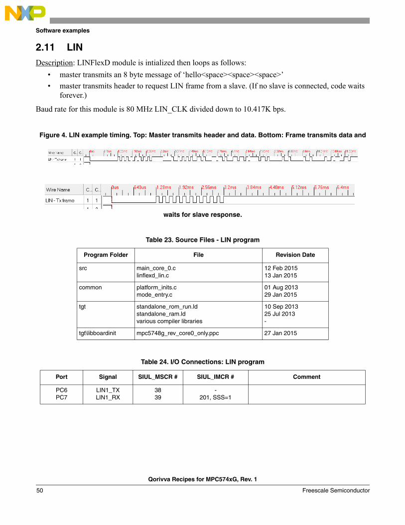
2.10 CANDescription: FlexCAN_0 transmits a CAN 2.0 B message to FlexCAN 1 at 500K baud. This example does not use interrupts, RX FIFO or DMA.
Key clocks and timing are:
• Clock sources:
— FlexCAN Control Host Interface (CHI) source : FS80 clock group, which is at 80 MHz here. Note that this frequency cannot be lower than the FlexCAN Protocol Engine clock source, which is 40 MHz in this example.
— FlexCAN Protocol Engine (PE clock) source: use external oscillator (FXOSC) of 40 MHz.
• CAN timing:
— Frame period in time quanta = Sync_Seg + Prop_Seg + Phase_Seg1 + Phase_Seg2
— # time quanta per bit rate period: choose 16 (typically 12-20)
— Sample point: choose 75% , which is 12 of 16 time quanta units
— Phase_Seg2 = # time quanta after sample point = 4
— Phase_Seg1 = Phase_Seg2 = 4
— Sync_Seg = 1
— Prop_Seg = # time quanta per period - Phase_Seg1 - Phase_Seg2 - SyncSeg = 16 -4 -4 -1 = 7
— Resync Jump Width = register field value RJW+1 = Phase_Seg2 if Phase_Seg2 < 4; else use 4. Use (RJW+1) = 4, so RJW = 3.
— ftq (time quanta frequency) = (16 time quanta/bit rate period) x (500K bit rate periods/sec) = 8 MHz
tgt\libboardinit mpc5748g_rev_core0_only.ppc 27 Jan 2015
Qorivva Recipes for MPC574xG, Rev. 1
Freescale Semiconductor46
Software examples
I/O Connection Notes:
This example can run on a Freescale evaluation board by connecting outputs of the two CAN transceivers. On the Freescale evaluation board to the three pin headers, P15 and P15:
• Connect CAN0-CANH on P15-1 to CAN1-CANH on P14-1
• Connect CAN0-CANL on P15-2 to CAN1-CANL on P14-2
• Connect a 60 ohm resistor between CANH and CANL to terminate the CAN bus
Design Summary:
• Perform general chip initilizations as in previous hello world projects including:
— Set sysclk to 160MHz PLL
— Enable clocks to peripherals FlexCAN0, FlexCAN1 in all RUN modes
• FlexCAN module initialization:
— Select clock source: Disable module (MDIS), and then select external osc (CLKSRC)
— Enable configuring module: Enable module (MDIS) and put into freeze mode (FRZ)
— Wait for freeze acknolwedge (FRZACK). This is generally good practice on freeze mode entry and exit.
— Optionally set additional module controls in Module Configuration Register (CAN_MCR)
— Initialize bit timing in Control 1 register (CAN_CTRL1)
— Optionally initialize CAN Bit Timing register (CAN_CBT), CAN FD Bit Timing register (CAN_FDCBT)
— Initialize message buffers
— Initialize mask registers
— Configure pads
— Negate Halt state for message buffers.
• Loop: Transmit and Receive message:
— Transmit message
– Fill in message buffer then set its code to activate
— Receive message
– Wait (poll) for message buffer flag (IFLAGx)
– Read message bufer
– Read timer to clear buffers
– Clear message buffer flag
Table 22. I/O Connections: FlexCAN program
Port Signal SIUL_MSCR # SIUL_IMCR # Comment
PB0PB1
PC10PC11
CAN0_TXCAN0_RXCAN1_TXCAN1_RX
16, SSS=117, SSS=242, SSS=143, SSS=3
-188
-189
Qorivva Recipes for MPC574xG, Rev. 1
Freescale Semiconductor 47
Software examples
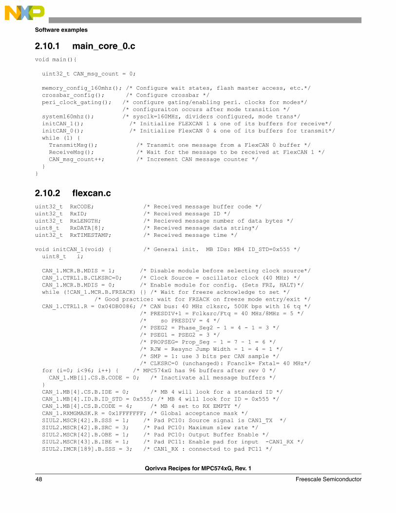
2.10.1 main_core_0.cvoid main(){
uint32_t CAN_msg_count = 0;
memory_config_160mhz(); /* Configure wait states, flash master access, etc.*/ crossbar_config(); /* Configure crossbar */ peri_clock_gating(); /* configure gating/enabling peri. clocks for modes*/ /* configuraiton occurs after mode transition */ system160mhz(); /* sysclk=160MHz, dividers configured, mode trans*/ initCAN_1(); /* Initialize FLEXCAN 1 & one of its buffers for receive*/ initCAN_0(); /* Initialize FlexCAN 0 & one of its buffers for transmit*/ while (1) { TransmitMsg(); /* Transmit one message from a FlexCAN 0 buffer */ ReceiveMsg(); /* Wait for the message to be received at FlexCAN 1 */ CAN_msg_count++; /* Increment CAN message counter */ }}
2.10.2 flexcan.cuint32_t RxCODE; /* Received message buffer code */uint32_t RxID; /* Received message ID */uint32_t RxLENGTH; /* Recieved message number of data bytes */uint8_t RxDATA[8]; /* Received message data string*/uint32_t RxTIMESTAMP; /* Received message time */
CAN_1.MCR.B.MDIS = 1; /* Disable module before selecting clock source*/ CAN_1.CTRL1.B.CLKSRC=0; /* Clock Source = oscillator clock (40 MHz) */ CAN_1.MCR.B.MDIS = 0; /* Enable module for config. (Sets FRZ, HALT)*/ while (!CAN_1.MCR.B.FRZACK) {} /* Wait for freeze acknowledge to set */ /* Good practice: wait for FRZACK on freeze mode entry/exit */ CAN_1.CTRL1.R = 0x04DB0086; /* CAN bus: 40 MHz clksrc, 500K bps with 16 tq */ /* PRESDIV+1 = Fclksrc/Ftq = 40 MHz/8MHz = 5 */ /* so PRESDIV = 4 */ /* PSEG2 = Phase_Seg2 - 1 = 4 - 1 = 3 */ /* PSEG1 = PSEG2 = 3 */ /* PROPSEG= Prop_Seg - 1 = 7 - 1 = 6 */ /* RJW = Resync Jump Width - 1 = 4 = 1 */ /* SMP = 1: use 3 bits per CAN sample */ /* CLKSRC=0 (unchanged): Fcanclk= Fxtal= 40 MHz*/ for (i=0; i<96; i++) { /* MPC574xG has 96 buffers after rev 0 */ CAN_1.MB[i].CS.B.CODE = 0; /* Inactivate all message buffers */ } CAN_1.MB[4].CS.B.IDE = 0; /* MB 4 will look for a standard ID */ CAN_1.MB[4].ID.B.ID_STD = 0x555; /* MB 4 will look for ID = 0x555 */ CAN_1.MB[4].CS.B.CODE = 4; /* MB 4 set to RX EMPTY */ CAN_1.RXMGMASK.R = 0x1FFFFFFF; /* Global acceptance mask */ SIUL2.MSCR[42].B.SSS = 1; /* Pad PC10: Source signal is CAN1_TX */ SIUL2.MSCR[42].B.SRC = 3; /* Pad PC10: Maximum slew rate */ SIUL2.MSCR[42].B.OBE = 1; /* Pad PC10: Output Buffer Enable */ SIUL2.MSCR[43].B.IBE = 1; /* Pad PC11: Enable pad for input -CAN1_RX */ SIUL2.IMCR[189].B.SSS = 3; /* CAN1_RX : connected to pad PC11 */
Qorivva Recipes for MPC574xG, Rev. 1
Freescale Semiconductor48
Software examples
CAN_1.MCR.R = 0x0000003F; /* Negate FlexCAN 1 halt state for 64 MBs */ while (CAN_1.MCR.B.FRZACK & CAN_1.MCR.B.NOTRDY) {} /* Wait to clear */ /* Good practice: wait for FRZACK on freeze mode entry/exit */}
void initCAN_0(void) { /* General init. No MB IDs iniialized */ uint8_ti;
CAN_0.MCR.B.MDIS = 1; /* Disable module before selecting clock source*/ CAN_0.CTRL1.B.CLKSRC=0; /* Clock Source = oscillator clock (40 MHz) */ CAN_0.MCR.B.MDIS = 0; /* Enable module for config. (Sets FRZ, HALT)*/ while (!CAN_0.MCR.B.FRZACK) {} /* Wait for freeze acknowledge to set */ CAN_0.CTRL1.R = 0x04DB0086; /* CAN bus: same as for CAN_1 */ for (i=0; i<96; i++) { /* MPC574xG has 96 buffers after rev 0 */ CAN_0.MB[i].CS.B.CODE = 0; /* Inactivate all message buffers */ } CAN_0.MB[0].CS.B.CODE = 8; /* Message Buffer 0 set to TX INACTIVE */ SIUL2.MSCR[16].B.SSS = 1; /* Pad PB0: Source signal is CAN0_TX */ SIUL2.MSCR[16].B.OBE = 1; /* Pad PB0: Output Buffer Enable */ SIUL2.MSCR[16].B.SRC = 3; /* Pad PB0: Maximum slew rate */ SIUL2.MSCR[17].B.IBE = 1; /* Pad PB1: Enable pad for input - CAN0_RX */ SIUL2.IMCR[188].B.SSS = 2; /* CAN0_RX: connected to pad PB1 */ CAN_0.MCR.R = 0x0000003F; /* Negate FlexCAN 0 halt state for 64 MB */ while (CAN_0.MCR.B.FRZACK & CAN_0.MCR.B.NOTRDY) {} /* Wait to clear */ /* Good practice: wait for FRZACK on freeze mode entry/exit */}
CAN_0.MB[0].CS.B.IDE = 0; /* Use standard ID length */ CAN_0.MB[0].ID.B.ID_STD = 0x555;/* Transmit ID is 0x555 */ CAN_0.MB[0].CS.B.RTR = 0; /* Data frame, not remote Tx request frame */ CAN_0.MB[0].CS.B.DLC = sizeof(TxData) -1 ; /*#bytes to transmit w/o null*/ for (i=0; i<sizeof(TxData); i++) { CAN_0.MB[0].DATA.B[i] = TxData[i]; /* Data to be transmitted */ } CAN_0.MB[0].CS.B.SRR = 1; /* Tx frame (not req'd for standard frame)*/ CAN_0.MB[0].CS.B.CODE =0xC; /* Activate msg. buf. to transmit data frame */ }
tgt\libboardinit mpc5748g_rev_core0_only.ppc 27 Jan 2015
Table 24. I/O Connections: LIN program
Port Signal SIUL_MSCR # SIUL_IMCR # Comment
PC6PC7
LIN1_TXLIN1_RX
3839
-201, SSS=1
Qorivva Recipes for MPC574xG, Rev. 1
Freescale Semiconductor50
Software examples
I/O Connection Notes:
This example can run on a Freescale evaluation board. One of two connections to the LIN 1 connector should be done:
• Connect 12V to the LIN 1 connector to power the transceiver. This enables the LIN transceiver to loop Tx back to Rx so entire transmit frames can be issued successfully.
• Optional: Connect a LIN tool to act as a LIN slave to respond to the master’s header issued in receiveLINframe() of this example.
Be sure the default jumpers are installed on LIN1 port of the EVB:
• J12: 1-2 (Rx), 3-4 (Tx)
• J13: 1-2 (Transceiver VSUP)
Design Summary:
• Perform general chip initilizations as in previous hello world projects including:
— Set sysclk to 160MHz PLL
— Enable clocks to peripherals LINFlex 1 in all RUN modes
– Load 8 bytes of data to buffere data registers: ‘hello’ plus three spaces. The LINFlex Buffer Data Registers use big Endian, so byte ordering is reversed.
1.Per MPC5748G Reference Manual, Rev 3, page 1847: Baud rate is calculate4d with the folowing formulat for bothreceiver and transmitter. Tx = Tx = LIN_CLK/(16 x LDIV).
– Wait for data receive complete flagNOTE: if no slave is connected then code waits forever here
– Put received data into buffer
– Clear data receive complete flag
— Increment a counter of LIN messages
2.11.1 main_core_0.cvoid peri_clock_gating (void) { MC_ME.RUN_PC[0].R = 0x00000000; /* gate off clock for all RUN modes */ MC_ME.RUN_PC[1].R = 0x000000FE; /* config. peri clock for all RUN modes */ MC_ME.PCTL[51].B.RUN_CFG = 0x1; /* LINFlex 1: select peri. cfg. RUN_PC[1]*/}
void main(){ uint32_t LIN_msg_count = 0; /* Count of LIN messages transmitted */
memory_config_160mhz(); /* Configure wait states, flash master access, etc.*/ crossbar_config(); /* Configure crossbar */ peri_clock_gating(); /* Configure gating/enabling peri. clocks for modes*/ /* Configuraiton occurs after mode transition */ system160mhz(); /* sysclk=160MHz, dividers configured, mode trans*/ initLINFlexD_1(); /* Initialize LINFlexD_1 as master */ while (1) { transmitLINframe(); /* Transmit one frame from master */ receiveLINframe(); /* Request data (requires extra LIN node)*/ LIN_msg_count++; /* Increment LIN message transmit count */ }}
Qorivva Recipes for MPC574xG, Rev. 1
Freescale Semiconductor52
Software examples
2.11.2 linflexd_lin.cvoid initLINFlexD_1 (void) { /* Master at 10.417K baud with 80MHz LIN_CLK */
LINFlexD_1.LINCR1.B.INIT = 1; /* Put LINFlex hardware in init mode */ LINFlexD_1.LINCR1.R= 0x00000311; /* Configure module as LIN master & header */ LINFlexD_1.LINIBRR.B.IBR= 480; /* Mantissa baud rate divider component */ /* Baud rate divider = 80 MHz LIN_CLK input / (16*10417K bps) ~=480 */ LINFlexD_1.LINFBRR.B.FBR = 0; /* Fraction baud rate divider comonent */ LINFlexD_1.LINCR1.R= 0x00000310; /* Change module mode from init to normal */ SIUL2.MSCR[38].B.SSS = 1; /* Pad PC7: Source signal is LIN1_TX */ SIUL2.MSCR[38].B.OBE = 1; /* Pad PC7: OBE=1. */ SIUL2.MSCR[38].B.SRC = 3; /* Pad PC7: Full strength slew rate */ SIUL2.MSCR[39].B.IBE = 1; /* Pad PC6: Enable pad for input */ SIUL2.IMCR[201].B.SSS = 1; /* LIN1_RX : connected to pad PC6 */}
void transmitLINframe (void) { /* Transmit one frame 'hello ' to ID 0x35*/
LINFlexD_1.BDRM.R = 0x2020206F; /* Load most significant bytes ' o' */ LINFlexD_1.BDRL.R = 0x6C6C6548; /* Load least significant bytes 'lleh' */ LINFlexD_1.BIDR.R = 0x00001E35; /* Init header: ID=0x35, 8 B, Tx, enh cksum*/ LINFlexD_1.LINCR2.B.HTRQ = 1; /* Request header transmission */ while (!LINFlexD_1.LINSR.B.DTF); /* Wait for data transfer complete flag */ LINFlexD_1.LINSR.R = 0x00000002; /* Clear DTF flag */ }
void receiveLINframe (void) { /* Request data from ID 0x15 */
uint8_t RxBuffer[8] = {0};uint8_t i;
LINFlexD_1.BIDR.R = 0x00001C15; /* Init header: ID=0x15, 8 B, Rx, enh cksum */ LINFlexD_1.LINCR2.B.HTRQ = 1; /* Request header transmission */ while (!LINFlexD_1.LINSR.B.DRF); /* Wait for data receive complete flag */
/* Code waits here if no slave response */ for (i=0; i<4;i++){ /* If received less than or equal 4 data bytes */
RxBuffer[i]= (LINFlexD_1.BDRL.R>>(i*8)); /* Fill buffer in reverse order */ } for (i=4; i<8;i++){ /* If received more than 4 data bytes: */
RxBuffer[i]= (LINFlexD_1.BDRM.R>>((i-4)*8)); /* Fill rest in reverse order */ } LINFlexD_1.LINSR.R = 0x00000004; /* Clear DRF flag */ }
Qorivva Recipes for MPC574xG, Rev. 1
Freescale Semiconductor 53
Software examples
2.12 UARTDescription: LINFlexD_2 module transmits and receives messages to a terminal. Transmission and reception is simply done one byte at a time without using the FIFO.
Key clocks and timing are:
• Clock sources and timing:
— LINFlexD_2 Control Host Interface (CHI) source : F80 clock group, which is at 80 MHz here.
• UART timing:
— For 80 MHz, generate a 57.6K baud rate
NOTE: LINFlexD modules have a transmit complete flag, UARTSR[DTFTFF]. The transmit function typically waits for this flag to set so it knows it is safe to load a new byte for transmission. There is one exception: after reset, this flag is automatically cleared, so the first charactrer should be sent without waiting for this flag to set.
This example’s implmenation uses a variable during LINFlexD initialization to indicate the first character has not been sent yet. The transmit function checks this variable. If the varible is set, it clears the variable and immediately sends the first byte without waiting for the UARTSR[DTFTFF] flag to set. Since the variable is now clear, subsequent transmissions will wait for UARTSR[DTFTFF] to set.
Vers
I/O Connection Notes:
This example can run on a Freescale evaluation board by connecting:
tgt\libboardinit mpc5748g_rev_core0_only.ppc 27 Jan 2015
Table 26. I/O Connections: lp_stop program
Port Signal SIUL_MSCR # SIUL_IMCR # Comment
PC8PC6
LIN2_TXLIN2_RX
4051
- 202, SSS=2
Qorivva Recipes for MPC574xG, Rev. 1
Freescale Semiconductor54
Software examples
• A USB type B cable from connector P17 on the evaluation board to your computer. A serial utility like TeraTerm can be used with settings: 57.6K baud, 8 bits, no parity. EVB default jumpers should be installed.
— Note: When power is lost to the EVB, the serial port connection to the PC is lost. To run the program after power loss (example power off/debugger detached), either restart the serial utility or reselect the serial port in the utility after the EVB powers up.
Design Summary:
• Perform general chip initilizations as in previous hello world projects including:
— Set sysclk to 160MHz PLL
— Enable clocks to peripherals LINFlexD2 in all RUN modes
• LINFlexD12 module initialization:
— Initialize as UART, 57.6K baud, 8 bits data, no parity
— Set variable to inidicate the transmit complete flag, UARTSR[DTFTFF], is still in reset state
— Configure pins
• Transmit a test message (transmit function waits for UARTSR[DTFTFF] to set before loading the character except for very first character after intialization)
• Loop:
— Wait for a character to be received
— Transmit back the same character
2.12.1 main_core_0.c void peri_clock_gating (void) { MC_ME.RUN_PC[0].R = 0x00000000; /* gate off clock for all RUN modes */ MC_ME.RUN_PC[1].R = 0x000000FE; /* config. peri clock for all RUN modes */ MC_ME.PCTL[52].B.RUN_CFG = 0x1; /* LINFlex 2: select peri. cfg. RUN_PC[1] */}
/************************************ Main ***********************************/
void main(){
unsigned char Input; memory_config_160mhz(); /* Config wait states, flash master access, etc*/ crossbar_config(); /* Config crossbar */ peri_clock_gating(); /* Config gating/enabling peri. clocks for modes*/ /* Configuraiton occurs after mode transition */ system160mhz(); /* sysclk=160MHz, dividers configured, mode trans*/ initLINFlexD_2( 80, 57600 ); /* Init LINFlex2: UART Mode 80MHz, 57600 Baud */ testLINFlexD_2(); /* Display a message on the terminal */ while (1) { Input = rxLINFlexD_2(); /* Wait for & receive one byte */ txLINFlexD_2( Input ); /* Transmit one byte */ }}
Qorivva Recipes for MPC574xG, Rev. 1
Freescale Semiconductor 55
Software examples
2.12.2 linflexd_uart.c/*****************************************************************************/** LINFLEX UART Driver** Notes:** 1. UARTCR bits can NOT be written until UARTCR.UART is SET** 2. There is no way to determine if the transmit buffer is** empty before the first data transmission. The DTF bit (Transmit Complete)** flag is the only indication that it's OK to write to the data buffer.** There is no way to set this bit in software. To set this bit, a transmit** must occur.*//*****************************************************************************/
/*****************************************************************************//*** Baud Rate = LINCLK / (16 x LFDIV)** LINCLK = BR x (16 x LFDIV)** LINCLK / (BR x 16) = LFDIV**** LFDIV = Mantissa.Fraction.** Mantissa = LINIBRR** Fraction = LINFBRR / 16**** Baud Rate = LINCLK / (16 x LINIBRR.(LINFBRR / 16))** LINIBRR.(LINFBRR / 16) = LINCLK / (BR x 16)** LINIBRR = Mantissa[LINCLK / (BR x 16)]** Remainder = LINFBRR / 16** LINFBRR = Remainder * 16** The Remainder is < 1, So how does the Remainder work during a divide?** May be best to use a table?**** For Refernce & Quick Tests** LINFLEX_x.LINIBRR.R = 416; // 9600 at 64MHz** LINFLEX_x.LINFBRR.R = 11;**** LINFLEX_x.LINIBRR.R = 781; // 9600 at 120MHz** LINFLEX_x.LINFBRR.R = 4;*//*****************************************************************************/
void initLINFlexD_2 ( unsigned int MegaHertz, unsigned int BaudRate ) { unsigned int Fraction; unsigned int Integer;
LINFlexD_2.LINCR1.B.INIT = 1; /* Enter Initialization Mode */ LINFlexD_2.LINCR1.B.SLEEP = 0; /* Exit Sleep Mode */ LINFlexD_2.UARTCR.B.UART = 1; /* UART Enable- Req'd before UART config.*/ LINFlexD_2.UARTCR.R = 0x0033; /* UART Ena, 1 byte tx, no parity, 8 data*/ LINFlexD_2.UARTSR.B.SZF = 1; /* CHANGE THIS LINE Clear the Zero status bit */ LINFlexD_2.UARTSR.B.DRFRFE = 1; /* CHANGE THIS LINE Clear DRFRFE flag - W1C */ BaudRate = (MegaHertz * 1000000) / BaudRate; Integer = BaudRate / 16;
Qorivva Recipes for MPC574xG, Rev. 1
Freescale Semiconductor56
Software examples
Fraction = BaudRate - (Integer * 16);
LINFlexD_2.LINIBRR.R = Integer; LINFlexD_2.LINFBRR.R = Fraction; LINFlexD_2.LINCR1.B.INIT = 0; /* Exit Initialization Mode */ UARTFirstTransmitFlag = 1; /* Indicate no Tx has taken place yet */ SIUL2.MSCR[40].B.SSS = 1; /* Pad PC8: Source signal is LIN2_TX */ SIUL2.MSCR[40].B.OBE = 1; /* Pad PC8: OBE=1. */ SIUL2.MSCR[40].B.SRC = 3; /* Pad PC8: Full strength slew rate */ SIUL2.MSCR[41].B.IBE = 1; /* Pad PC6: Enable pad for input */ SIUL2.IMCR[202].B.SSS = 2; /* LIN2_RX : connected to pad PC9 */}/*****************************************************************************/
char message[] = "Welcome to MPC5748G! ";
void testLINFlexD_2( void ) { /* Display message to terminal */ int i, size; size = sizeof(message); for (i = 0; i < size; i++) { txLINFlexD_2(message[i]); } txLINFlexD_2(13); /* Carriage return */ txLINFlexD_2(10); /* Line feed */}/*****************************************************************************/
unsigned char rxLINFlexD_2() { while (LINFlexD_2.UARTSR.B.DRFRFE == 0); /* Wait for dta reception complete*/ LINFlexD_2.UARTSR.R &= UART_DRFRFE; /* Clear data receptoin flag W1C */ return( LINFlexD_2.BDRM.B.DATA4 ); /* Read byte of Data */}/*****************************************************************************/
void txLINFlexD_2( unsigned char Data ) { if( UARTFirstTransmitFlag ) { /* 1st byte transmit after init: */ UARTFirstTransmitFlag = 0; /* Clear variable */ } else { /* Normal tranmit (not 1st time): */ while (LINFlexD_2.UARTSR.B.DTFTFF == 0); /* Wait for data trans complete*/ LINFlexD_2.UARTSR.R &= UART_DTFTFF; /* Clear DTFTFF flag - W1C */ } LINFlexD_2.BDRL.B.DATA0 = Data; /* Transmit 8 bits Data */}/*****************************************************************************/
unsigned char checkLINFlexD_2() { /* Optional utility for status check */ return( LINFlexD_2.UARTSR.B.DRFRFE ); /* Return Receive Buffer Status */}/*****************************************************************************/
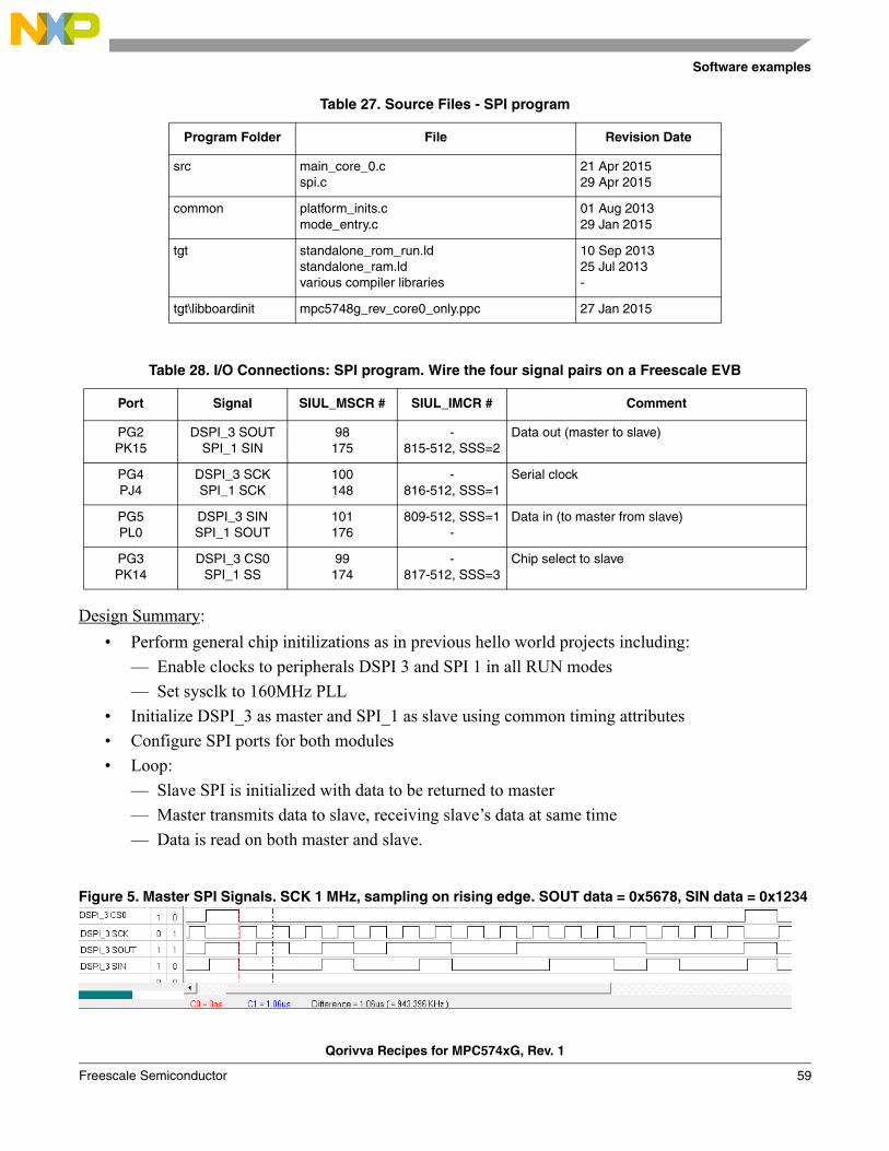
2.13 SPIDescription: DSPI_3 module, configured as master, transmits data to a SPI_1 module that is configured as a slave. Transmissions are implemented using repeated software issued commands without interrupts or DMA. Baud rate is 1 MHz.
Clock and Timing Attributes Register (CTARx): Both modules will use the same timing attributes below even though the slave module does not use some of the attributes. Both modules also share the same baud rate clock input source of F80 clock group at 80 MHz, which has a 12.5 nsec period. (Some DSPI and SPI modules use a different input source frequency!) The CTAR value of 0x7802_1004 is used here to provide the following timing and attributes:
• Frame Size (FMSZ) = 16 bits
• LSB First (LSBFE): MSB, not LSB, will be sent first here
• Clock Polarity (CPOL): low inactive state
• Clock Phase (CPHA): capture data on leading edge (rising edge)
• SCK Baud Rate = (fF80 / (PBR prescaler of 5) x ((1 + DBR of 0) / (BR scaler of 16))= (80 MHz / 5) x ((1 + 0 ) /(16)= 1 MHz (1 usec period)
• PCS to SCK Delay (tCSC) = (F80 period) x (PCSSCK prescaler of 1) x (CSSCK delay scale of 4)= 12.5 nsec x 1 x 2= 50 nsec
• After SCK Delay (tASC) = (F80 period) x (PASC prescaler of 1) x (ASC delay scale of 2)= 12.5 nsec x 1 x 2= 25 nsec
• Delay after Transfer(tDT) = (F80 period) x (PDT prescaler of 1) x (DT delay scale of 2)= 12.5 nsec x 1 x 2= 25 nsec
TIP: Be sure to have adequate delay between the sampling edge of SCK and PCS. In this example SCK samples on the leading edge, which is the first edge after PCS goes active. Therefore 50 nsec (tCSC) after PCS the master samples its SIN input from the slave. The slave must have its SOUT output changed within that short time. On the Freescale EVB using simple jumper wires the first bit was often improperly read when tCSC was 25 nsec, but worked properly when tCSC was 50 nsec.
The actual SPI commands consist of the fields below:
• Continuous Peripheral Chip Select: Not used here, so PCS is inactive between transfers
• Clock and Transfer Register: CTAR 0 is required for slave SPIs. Master will also use CTAR 0.
• End of Queue: EOQ bit is set for last transfer, which is the only transfer in this example.
• Transfer Data: The slave will respond with data 0x1234. The master transmits 0x5678.
Pad slew rate control is imporant for fast SPI baud rates. The pad register field SIUL2_MSCRx[SRC] is set to the maximum slew rate.
Qorivva Recipes for MPC574xG, Rev. 1
Freescale Semiconductor58
Software examples
Design Summary:
• Perform general chip initilizations as in previous hello world projects including:
— Enable clocks to peripherals DSPI 3 and SPI 1 in all RUN modes
— Set sysclk to 160MHz PLL
• Initialize DSPI_3 as master and SPI_1 as slave using common timing attributes
• Configure SPI ports for both modules
• Loop:
— Slave SPI is initialized with data to be returned to master
— Master transmits data to slave, receiving slave’s data at same time
— Data is read on both master and slave.
Figure 5. Master SPI Signals. SCK 1 MHz, sampling on rising edge. SOUT data = 0x5678, SIN data = 0x1234
tgt\libboardinit mpc5748g_rev_core0_only.ppc 27 Jan 2015
Table 28. I/O Connections: SPI program. Wire the four signal pairs on a Freescale EVB
Port Signal SIUL_MSCR # SIUL_IMCR # Comment
PG2PK15
DSPI_3 SOUTSPI_1 SIN
98175
-815-512, SSS=2
Data out (master to slave)
PG4PJ4
DSPI_3 SCKSPI_1 SCK
100148
-816-512, SSS=1
Serial clock
PG5PL0
DSPI_3 SINSPI_1 SOUT
101176
809-512, SSS=1-
Data in (to master from slave)
PG3PK14
DSPI_3 CS0SPI_1 SS
99174
-817-512, SSS=3
Chip select to slave
Qorivva Recipes for MPC574xG, Rev. 1
Freescale Semiconductor 59
Software examples
2.13.1 main_core_0.c void peri_clock_gating (void) { MC_ME.RUN_PC[0].R = 0x00000000; /* gate off clock for all RUN modes */ MC_ME.RUN_PC[1].R = 0x000000FE; /* config. peri clock for all RUN modes */ MC_ME.PCTL[43].B.RUN_CFG = 0x1; /* DSPI 2: select peri. cfg. RUN_PC[1] */ MC_ME.PCTL[97].B.RUN_CFG = 0x1; /* SPI 1: select peri. cfg. RUN_PC[1] */}
/************************************ Main ***********************************/
void main(){ unsigned int i = 0; memory_config_160mhz(); /* Config wait states, flash master access, etc*/ crossbar_config(); /* Config crossbar */ peri_clock_gating(); /* Config gating/enabling peri. clocks for modes*/ /* Configuraiton occurs after mode transition */ system160mhz(); /* sysclk=160MHz, dividers configured, mode trans*/ init_DSPI_3(); /* Initialize DSPI_0 as master SPI and init CTAR0 */ init_SPI_1(); /* Initialize DSPI_1 as Slave SPI and init CTAR0 */ init_spi_ports(); /* DSPI3 Master, SPI_1 Slave */
while( 1 ) { SPI_1.PUSHR.PUSHR.R = 0x00001234; /* Initialize slave DSPI_1's response to master */ DSPI_3.PUSHR.PUSHR.R = 0x08015678; /* Transmit data from master to slave SPI with EOQ */ read_data_SPI_1(); /* Read data on slave DSPI */ read_data_DSPI_3(); /* Read data on master DSPI */ i++; }}
2.13.2 spi.cunsigned int RecDataMaster;unsigned int RecDataSlave;
/*****************************************************************************//* There are only 2 options available on the Freescale MPC5748G EVB** the "x" signifies the channel used** ** DSPI_3 MASTER** CLK PG4x PH12** SOUT PG2x PH11** SIN PG5x PI11** SS/CS0 PG3xPH13**** SPI_1 SLAVE** CLK PJ4x** SOUT PH15 PK13 PL0x PP6** SIN PJ1 PK15x** SS/CS0 PI6 PJ2 PK14x *//*****************************************************************************/
Qorivva Recipes for MPC574xG, Rev. 1
Freescale Semiconductor60
Software examples
void init_spi_ports() { /* Master - DSPI_3 */ SIUL2.MSCR[98].B.SSS = 2; /* Pad PG2: Source signal is DSPI_3 SOUT */ SIUL2.MSCR[98].B.OBE = 1; /* Pad PG2: OBE=1. */ SIUL2.MSCR[98].B.SRC = 3; /* Pad PG2: Full strength slew rate */ SIUL2.MSCR[100].B.SSS = 2; /* Pad PG4: Source signal is DSPI_3 CLK */ SIUL2.MSCR[100].B.OBE = 1; /* Pad PG4: OBE=1. */ SIUL2.MSCR[100].B.SRC = 3; /* Pad PG4: Full strength slew rate */ SIUL2.MSCR[101].B.IBE = 1; /* Pad PG5: Enable pad for input DSPI_3 SIN */ SIUL2.IMCR[809-512].B.SSS = 1; /* Pad PG5: connected to pad PG5 */
SIUL2.MSCR[99].B.SSS = 2; /* Pad PG3: Source signal is DSPI_3 CS0 */ SIUL2.MSCR[99].B.OBE = 1; /* Pad PG3: OBE=1. */ SIUL2.MSCR[99].B.SRC = 3; /* Pad PG3: Full strength slew rate */ /* Slave - SPI_1 */ SIUL2.MSCR[148].B.SSS = 1; /* Pad PJ4: Source signal is SPI_1 CLK */ SIUL2.MSCR[148].B.IBE = 1; /* Pad PJ4: IBE=1. */ SIUL2.IMCR[816-512].B.SSS = 1; /* Pad PJ4: SPI_1 CLK */ SIUL2.MSCR[176].B.SSS = 1; /* Pad PL0: Source signal is SPI_1 SOUT */ SIUL2.MSCR[176].B.OBE = 1; /* Pad PL0: OBE=1. */ SIUL2.MSCR[176].B.SRC = 3; /* Pad PL0: Full strength slew rate */ SIUL2.MSCR[175].B.IBE = 1; /* Pad PK15: Enable pad for input SPI_1 SIN */ SIUL2.IMCR[815-512].B.SSS = 2; /* Pad PK15: connected to pad */
SIUL2.MSCR[174].B.IBE = 1; /* Pad PK14: IBE=1. SPI_1 SS */ SIUL2.IMCR[817-512].B.SSS = 3; /* Pad PK14: connected to pad */}
void init_DSPI_3(void) { DSPI_3.MCR.R = 0x80010001; /* Configure DSPI as master */ DSPI_3.MODE.CTAR[0].R = 0x78021004; /* Configure CTAR0 */ DSPI_3.MCR.B.HALT = 0x0; /* Exit HALT mode: go from STOPPED to RUNNING state*/}
void read_data_DSPI_3(void) { while (DSPI_3.SR.B.RFDF != 1){} /* Wait for Receive FIFO Drain Flag = 1 */ RecDataSlave = DSPI_3.POPR.R; /* Read data received by slave SPI */ DSPI_3.SR.R = 0xFCFE0000; /* Clear ALL status flags by writing 1 to them */}
void init_SPI_1(void) { SPI_1.MCR.R = 0x00010001; /* Configure DSPI_1 as slave */ SPI_1.MODE.CTAR[0].R = 0x78021004; /* Configure CTAR0 */ SPI_1.MCR.B.HALT = 0x0; /* Exit HALT mode: go from STOPPED to RUNNING state*/}
void read_data_SPI_1(void) { while (SPI_1.SR.B.RFDF != 1){} /* Wait for Receive FIFO Drain Flag = 1 */ RecDataMaster = SPI_1.POPR.R; /* Read data received by master SPI */ SPI_1.SR.R = 0xFCFE0000; /* Clear ALL status flags by writing 1 */}
Qorivva Recipes for MPC574xG, Rev. 1
Freescale Semiconductor 61
Software examples
2.14 SPI + DMADescription: DSPI_3 module, configured as master, transmits a 256 element array of bytes to a SPI_1 module using DMA. Transmissions are implemented using DMA. A single byte is transferred each DMA request. Baud rate is 1 MHz.
Clock and Timing Attributes Register (CTARx): Both modules will use the same timing attributes below even though the slave module does not use some of the attributes. Both modules also share the same baud rate clock input source of F80 clock group at 80 MHz, which has a 12.5 nsec period. (Some DSPI and SPI modules use a different input source frequency!) The CTAR value of 0xB800_1111 is used here to provide the following timing and attributes:
• Frame Size (FMSZ) = 8 bits
• LSB First (LSBFE): MSB, not LSB, will be sent first here
• Clock Polarity (CPOL): low inactive state
• Clock Phase (CPHA): capture data on leading edge (rising edge)
• SCK Baud Rate = (fF80 / (PBR prescaler of 2) x ((1 + DBR of 1) / (BR scaler of 4))= (80 MHz / 2) x ((1 + 1) /(4)= 20MHz (50 nsec period)
• PCS to SCK Delay (tCSC) = (F80 period) x (PCSSCK prescaler of 1) x (CSSCK delay scale of 4)= 12.5 nsec x 1 x 2= 50 nsec
• After SCK Delay (tASC) = (F80 period) x (PASC prescaler of 1) x (ASC delay scale of 4)= 12.5 nsec x 1 x 4= 50 nsec
• Delay after Transfer(tDT) = (F80 period) x (PDT prescaler of 1) x (DT delay scale of 4)= 12.5 nsec x 1 x 4= 50 nsec
TIP: Be sure to have adequate delay between the sampling edge of SCK and PCS. In this example SCK samples on the leading edge, which is the first edge after PCS goes active.
The actual SPI commands consist of the fields below:
• Continuous Peripheral Chip Select: Not used here, so PCS is inactive between transfers
• Clock and Transfer Register: CTAR 0 is required for slave SPIs. Master will also use CTAR 0.
• End of Queue: EOQ bit is set for last transfer, which is the only transfer in this example.
• Transfer Data: The slave will respond with zero. The master transmits an increasing value from an 256 byte arrary that start at 0 and goes to 255.
Pad slew rate control is imporant for fast SPI baud rates. The pad register field SIUL2_MSCRx[SRC] is set to the maximum slew rate.
Qorivva Recipes for MPC574xG, Rev. 1
Freescale Semiconductor62
Software examples
Design Summary:
• Perform general chip initilizations as in previous hello world projects including:
— Enable clocks to peripherals DSPI 3 and SPI 1 in all RUN modes
— Set sysclk to 160MHz PLL
• Configure PBridge to allow DMA and other masters RW and user-level access
• Configure crossbar slave ports for PBridges and flash port 2 to give DMA highest priority
• Initialize eDMA Multiplexer to connect eDMA channels to DSPI_3 transmit and SPI_1 receive
• Initialize eDMA channels used and arbitration
• Initialize DSPI_3 as master and SPI_1, their ports and exit DSPI/SPI HALT mode
• Enable DMA channels for SPI_1, DSPI_3 to start SPI to SPI communication.
• Wait for the end of the SPI transmit queue status flag.
tgt\libboardinit mpc5748g_rev_core0_only.ppc 27 Jan 2015
Table 30. I/O Connections: SPI program. Wire the four signal pairs on a Freescale EVB
Port Signal SIUL_MSCR # SIUL_IMCR # Comment
PG2PK15
DSPI_3 SOUTSPI_1 SIN
98175
-815-512, SSS=2
Data out (master to slave)
PG4PJ4
DSPI_3 SCKSPI_1 SCK
100148
-816-512, SSS=1
Serial clock
PG5PL0
DSPI_3 SINSPI_1 SOUT
101176
809-512, SSS=1-
Data in (to master from slave)
PG3PK14
DSPI_3 CS0SPI_1 SS
99174
-817-512, SSS=3
Chip select to slave
Qorivva Recipes for MPC574xG, Rev. 1
Freescale Semiconductor 63
Software examples
Figure 6. Master SPI Signals. SCK 20 MHz, sampling on rising edge. SOUT data = 0 to 0x255, SIN data = 0
Qorivva Recipes for MPC574xG, Rev. 1
Freescale Semiconductor64
Software examples
2.14.1 main_core_0.c void peri_clock_gating (void) { MC_ME.RUN_PC[0].R = 0x00000000; /* gate off clock for all RUN modes */ MC_ME.RUN_PC[1].R = 0x000000FE; /* config. peri clock for all RUN modes */ MC_ME.PCTL[43].B.RUN_CFG = 0x1; /* DSPI 2: select peri. cfg. RUN_PC[1] */ MC_ME.PCTL[97].B.RUN_CFG = 0x1; /* SPI 1: select peri. cfg. RUN_PC[1] */ MC_ME.PCTL[90].B.RUN_CFG = 0x1; /* DMAMUX: select peri. cfg. RUN_PC[1] */}
void bridges_config (void) { AIPS_A.MPRA.R |= 0x77777770; /* All masters have RW & user level access */ AIPS_A.MPRB.R |= 0x07777700; /* All masters have RW & user level access */ AIPS_B.MPRA.R |= 0x77777770; /* All masters have RW & user level access */ AIPS_B.MPRB.R |= 0x07777700; /* All masters have RW & user level access */}
/************************************ Main ***********************************/
void main() { unsigned int i = 0; memory_config_160mhz(); /* Config wait states, flash master access, etc*/ peri_clock_gating(); /* Config gating/enabling peri. clocks for modes*/ /* Configuraiton occurs after mode transition */ system160mhz(); /* sysclk=160MHz, dividers configured, mode trans */ bridges_config(); /* Config PBridge(s) access rights and priorities */ crossbar_config_DMA_highest(); /* PBridges, flash port 2: DMA highest priority */
init_dma_mux(); /* DMA MUX for SPI_1 Slave */ init_edma_tcd_16(); /* DMA Channel for SPI_1 Slave */ init_edma_tcd_17(); /* DMA Channel for DSPI_3 Master */ init_edma_channel_arbitration(); /* DMA Channel priorities */
init_dspi_3(); /* Initialize DSPI_0 as master SPI and init CTAR0 */ init_spi_1(); /* Initialize DSPI_1 as Slave SPI and init CTAR0 */ init_spi_ports(); /* DSPI3 Master, SPI_1 Slave */
DSPI_3.MCR.B.HALT = 0x0; /* Exit HALT mode: go from STOPPED */ /* to RUNNING state to start transfers */ EDMA.SERQ.R = 16; /* Enable EDMA channel 16 SPI_1 RX */ EDMA.SERQ.R = 17; /* Enable EDMA channel 17 DSPI_3 TX*/
while( DSPI_3.SR.B.EOQF != 1 ){} /* Wait until the End Of DSPI Queue: */ /* All data is transmitted & received by DMA */ while( 1 ) { i++; }}
Qorivva Recipes for MPC574xG, Rev. 1
Freescale Semiconductor 65
Software examples
2.14.2 spi.cvoid init_spi_ports(){ /* Master - DSPI_3 */ SIUL2.MSCR[98].B.SSS = 2; /* Pad PG2: Source signal is DSPI_3 SOUT */ SIUL2.MSCR[98].B.OBE = 1; /* Pad PG2: OBE=1. */ SIUL2.MSCR[98].B.SRC = 3; /* Pad PG2: Full strength slew rate */ SIUL2.MSCR[100].B.SSS = 2; /* Pad PG4: Source signal is DSPI_3 CLK */ SIUL2.MSCR[100].B.OBE = 1; /* Pad PG4: OBE=1. */ SIUL2.MSCR[100].B.SRC = 3; /* Pad PG4: Full strength slew rate */ SIUL2.MSCR[101].B.IBE = 1; /* Pad PG5: Enable pad for input DSPI_3 SIN */ SIUL2.IMCR[809-512].B.SSS = 1; /* Pad PG5: connected to pad PG5 */
SIUL2.MSCR[99].B.SSS = 2; /* Pad PG3: Source signal is DSPI_3 CS0 */ SIUL2.MSCR[99].B.OBE = 1; /* Pad PG3: OBE=1. */ SIUL2.MSCR[99].B.SRC = 3; /* Pad PG3: Full strength slew rate */ /* Slave - SPI_1 */ SIUL2.MSCR[148].B.SSS = 1; /* Pad PJ4: Source signal is SPI_1 CLK */ SIUL2.MSCR[148].B.IBE = 1; /* Pad PJ4: IBE=1. */ SIUL2.IMCR[816-512].B.SSS = 1; /* Pad PJ4: SPI_1 CLK */ SIUL2.MSCR[176].B.SSS = 1; /* Pad PL0: Source signal is SPI_1 SOUT */ SIUL2.MSCR[176].B.OBE = 1; /* Pad PL0: OBE=1. */ SIUL2.MSCR[176].B.SRC = 3; /* Pad PL0: Full strength slew rate */ SIUL2.MSCR[175].B.IBE = 1; /* Pad PK15: Enable pad for input SPI_1 SIN */ SIUL2.IMCR[815-512].B.SSS = 2; /* Pad PK15: connected to pad */
SIUL2.MSCR[174].B.IBE = 1; /* Pad PK14: IBE=1. SPI_1 SS */ SIUL2.IMCR[817-512].B.SSS = 3; /* Pad PK14: connected to pad */}
void init_edma_tcd_16() { /* This is for SPI_1 Receive */ /* SADDR Note: 1 byte is transferred in this TCD on each DMA request (minor loop). */ /* The byte is 4th one in the 32-bit POPR register. */ /* Therefore a +3 byte offset is added to POPR address for the source address SADDR */ EDMA.TCD[16].SADDR.R = ((unsigned int)&SPI_1.POPR.R) + 3; /* Load address of source data */ EDMA.TCD[16].ATTR.B.SSIZE = 0; /* Read 2**0 = 1 byte per transfer */ EDMA.TCD[16].ATTR.B.SMOD = 0; /* Source modulo feature not used */ EDMA.TCD[16].SOFF.R = 0; /* After transfer, add 0 to src addr */ EDMA.TCD[16].SLAST.R = 0; /* No addr adjustment after major loops */
EDMA.TCD[16].DADDR.R = (unsigned int)&ReceiveBuffer; /* Destination address */ EDMA.TCD[16].ATTR.B.DSIZE = 0; /* Write 2**0 = 1 byte per transfer */ EDMA.TCD[16].ATTR.B.DMOD = 0; /* Destination modulo feature not used */ EDMA.TCD[16].DOFF.R = 1; /* Increment destination addr by 1 */ /* If repeating major loop, subtract NUMBER_OF_BYTES from dest. addr. */ EDMA.TCD[16].DLASTSGA.R = 0; /* No addr adjustment after major loop */
/* If repeating major loop, set this to 0 to keep the channel enabled */ EDMA.TCD[16].CSR.B.DREQ = 1; /* Disable channel when major loop is done*/ EDMA.TCD[16].NBYTES.MLNO.R = 1; /* NBYTES - Transfer 1 byte per minor loop */ EDMA.TCD[16].CITER.ELINKNO.B.ELINK = 0; /* No Enabling channel LINKing */ EDMA.TCD[16].CITER.ELINKNO.B.CITER = NUMBER_OF_BYTES; /* Init. current interaction count */ EDMA.TCD[16].BITER.ELINKNO.B.ELINK = 0; /* No Enabling channel LINKing */ EDMA.TCD[16].BITER.ELINKNO.B.BITER = NUMBER_OF_BYTES; /* Minor loop iterations */ EDMA.TCD[16].CSR.B.MAJORELINK = 0; /* Dynamic program is not used */ EDMA.TCD[16].CSR.B.ESG = 0; /* Scatter Gather not Enabled */ EDMA.TCD[16].CSR.B.BWC = 0; /* Default bandwidth control- no stalls */ EDMA.TCD[16].CSR.B.INTHALF = 0; /* No interrupt when major count half complete */ EDMA.TCD[16].CSR.B.INTMAJOR = 0; /* No interrupt when major count completes */ EDMA.TCD[16].CSR.B.MAJORLINKCH = 0; /* No link channel # used */ EDMA.TCD[16].CSR.B.START = 0; /* Initialize status flags START, DONE, ACTIVE */ EDMA.TCD[16].CSR.B.DONE = 0; EDMA.TCD[16].CSR.B.ACTIVE = 0;}
Qorivva Recipes for MPC574xG, Rev. 1
Freescale Semiconductor 67
Software examples
void init_edma_tcd_17() { /* This is for DSPI_3 Transmit */ EDMA.TCD[17].SADDR.R = (unsigned int)&TransmitBuffer; /* Source address */ EDMA.TCD[17].ATTR.B.SSIZE = 2; /* Read 2**2 = 4 bytes per transfer */ EDMA.TCD[17].ATTR.B.SMOD = 0; /* Source modulo feature not used */ EDMA.TCD[17].SOFF.R = 4; /* After transfer, add 0 to src addr */ EDMA.TCD[17].SLAST.R = 0; /* No addr adjustment after major loop */
EDMA.TCD[17].DADDR.R = (unsigned int)&DSPI_3.PUSHR.PUSHR.R; /* Destination address */ EDMA.TCD[17].ATTR.B.DSIZE = 2; /* Write 2**0 = 1 byte per transfer */ EDMA.TCD[17].ATTR.B.DMOD = 0; /* Destination modulo feature not used */ EDMA.TCD[17].DOFF.R = 0; /* No addr adjustment after major loop */ /* If repeating major loop, subtract NUMBER_OF_BYTES from dest. addr. */ EDMA.TCD[17].DLASTSGA.R = 0; /* After major loop, adjust the destination address */
/* If repeating major loop, set this to 0 to keep the channel enabled */ EDMA.TCD[17].CSR.B.DREQ = 1; /* Disable channel when major loop is done*/ EDMA.TCD[17].NBYTES.MLNO.R = 4; /* NBYTES - Transfer 1 byte per minor loop */ EDMA.TCD[17].CITER.ELINKNO.B.ELINK = 0; /* No Enabling channel LINKing */ EDMA.TCD[17].CITER.ELINKNO.B.CITER = NUMBER_OF_BYTES; /* Init. current interaction count */ EDMA.TCD[17].BITER.ELINKNO.B.ELINK = 0; /* No Enabling channel LINKing */ EDMA.TCD[17].BITER.ELINKNO.B.BITER = NUMBER_OF_BYTES; /* Minor loop iterations */ EDMA.TCD[17].CSR.B.MAJORELINK = 0; /* Dynamic program is not used */ EDMA.TCD[17].CSR.B.ESG = 0; /* Scatter Gather not Enabled */ EDMA.TCD[17].CSR.B.BWC = 0; /* Default bandwidth control- no stalls */ EDMA.TCD[17].CSR.B.INTHALF = 0; /* No interrupt when major count half complete */ EDMA.TCD[17].CSR.B.INTMAJOR = 0; /* No interrupt when major count completes */ EDMA.TCD[17].CSR.B.MAJORLINKCH = 0; /* No link channel # used */ EDMA.TCD[17].CSR.B.START = 0; /* Initialize status flags START, DONE, ACTIVE */ EDMA.TCD[17].CSR.B.DONE = 0; EDMA.TCD[17].CSR.B.ACTIVE = 0;}
void init_edma_channel_arbitration (void) { /* Use default fixed arbitration */ EDMA.CR.R = 0x0000E400; /* Fixed priority arbitration for groups, channels */ EDMA.DCHPRI[0].R = 0x00; /* Grp 0 chan 00, no suspension, no premption */ EDMA.DCHPRI[1].R = 0x01; /* Grp 0 chan 01, no suspension, no premption */
... etc. for arbitration of all 32 DMA channels ...
EDMA.DCHPRI[31].R = 0x1F; /* Grp 1 chan 15, no suspension, no premption */ }
Qorivva Recipes for MPC574xG, Rev. 1
Freescale Semiconductor68
Startup code
3 Startup code
3.1 List of initializationsCompilers normally have wizards or sample startup code which include many if not all of these initializations. In general, this code should be considered as a starting point. Users should review the initializations to see if any are missing or if changes are desired.
Table 31. List of initializations done by cores.
When Done
ItemBoot Core
Add’l Cores
Comment
Compile boot header (in flash) - - Identifies which core(s) boot & their start vectors.
Before main
Watchdog disable x - All three watchdogs for the three cores are disabled here in these examples.
SRAM initialization x - Writing to SRAM before use is required to initialize ECC bits.
Set MSR[ME] = 1Set IVPR = start of SRAM x x
Enables machine check core exception and exception vector address prefix. Now checkstop, such as from ECC error with MSE[EE]=0, will cause machine check.
Initialize caches
x x
If instruction and data cache exists, initialize them. Optimization tip: lock critical code, such as an interrupt handler prologue and epilouge in instruction cache.Note: peripherals are hardwired to be cache inhibited in the AIPS.
Enable Branch Target Buffers (BTB) x x
Each core has branch target buffers to improve branch instruction execution. The buffers are in RAM, so they initially need to be marked invalid when they are enabled.
Initialize stack pointers x x Provide each core with a unique stack pointer
Initialize sda, sda2 x x Common sda and sda2 for all cores are implemented in these examples
Initialize variables x x Copy Initialized variables from ROM to RAM
After main
Configure memory
x -
Flash wait states and other attributes need to be Initialized. Writing to flash attribute registers should not be executed while any master is accessing flash, so code is executed from RAM.RAM wait states are typically not required for MPC5748G.
Configure crossbar x - If desired, crossbar default configuration can be changed.
Enable clocks to desired peripherals
x -
To conserve power, after reset clocks to peripherals are gated off. For a peripheral to get a clock, it’s Peripheral Control register (ME_PCTLx) must select peripheral configuration registers which select modes for clocking, then a mode transition occur to enable the selected clocking.
Configure clock dividers and system clock
x -Configure clock dividers to peripherals for target system clock frequency, configure PLL and perform mode transition to activate PLL as system clock.
Start other coresx -
For each core, initialize start address and other configurations then perform mode entry to start other core. Each core does it’s own intializations.
Qorivva Recipes for MPC574xG, Rev. 1
Freescale Semiconductor 69
Startup code
3.2 Boot headerA boot header is required in flash to specify which core(s) start and the starting address for core(s). The boot header is placed in one of several flash addresses. After reset, the internal BAF code searches those addresses for a boot identifier (0x5A) to identify the boot header. The search order is looking from the lowest to highest possible boot header addresses.
Below is the boot header used for these examples.
3.3 Startup initializations before boot core’s mainSince before main there are many software tasks that are common to all microcontrollers, compilers often have a set of shared common files plus one file for initializations specific to the microcontroller. The GHS file in these examples specific to this microcontroller is mpc5574G_rev1.ppc. The following table is a summary of the functions in the code flow from reset to main and which file has those functions.
Table 32. Boot header
Section Address Offset Long value Description
.boot_header 0x0 0x005A 0002 Boot ID and enable booting core 0
0x4 0x0 Core 2 reset vector
0x8 0x0 -
0xC 0x0 -
0x10 __ghs_rombootcodestart Core 0 reset vector
0x14 0x0 Core 1 reset vector
0x18 0x0 -
0x1C 0x0 -
Table 33. Startup summary implemented before main in GHS projects (all executed from boot core)
Step mpc5748G_rev1.ppc crt0.ppc ind_crt1.c
reset boot_header at 0xF8_C000: enables only core 0 with vector of __ghsrombootcorestart which is _start
- -
1 - _start • bl __ghs_board_memory_init
-
2 __ghs_board_memory_init: • Disable watchdogs SWT0:2 • ECC initialization of shared SRAM • b __ghs_e200z4304_core_init
- -
Qorivva Recipes for MPC574xG, Rev. 1
Freescale Semiconductor70
Startup code
3.4 Startup initializations after boot core’s mainAfter the boot core reaches main, consider which other general initializations should take place before starting other cores. These examples perform clock and PLL initialization before starting more cores.
If another core is not running, it can be started as follows:
1. Enable which RUN and/or low power modes the core will run in the core’s Mode Entry core control register.
2. Load the address for that core to start code execution in the core’s Mode Entry core address register.
3. Performing a mode transition to a mode (even if the same one) where that core is enabled to run.
#define PFLASH_PFCR1_VALUE_16MHz 0x00152117 /* Flash port p0 configuration: */ /* Port 0 prefetch enables for masters 0,3,5 (core I-busses) only, */ /* APC=1 Pipelined access can be intiazted 1 cyc before prev data valid, */ /* RWSC=1 Read Wait State Control: 1 add'l wait states (16 MHz), */ /* P0_DPFEN=0 No prefetching is triggerd by a data read access, */ /* P0_IPFEN=1 Prefetching may be triggered by any instruction read access*/ /* P0_PFLIM=3 Prefetch on miss or hit, */ /* P0_BFEN=1 Line read buffers are enabled. */#define PFLASH_PFCR1_VALUE_160MHz 0x00152417 /* Flash port p0 configuration: */ /* RWSC=4 r Read Wait State Control: 4 add'l wait states (160 MHz), */ /* All other fields same as for 16 MHz. */#define PFLASH_PFCR2_VALUE_BASIC 0x00150017 /* Flash port p1 configuration: */ /* Configured same as Port 0 except for not present fields of APC, RWSC. */#define PFLASH_PFCR3_VALUE_BASIC 0x00000000 /* Flash way cfg, arb., BAF dis. */ /* All ports have both buffers available for any flash access, */ /* BAF_DIS=0 Executable access to BAF flash region is allowed, */ /* ARBM=0 Fixed priority arbitration with AHB p0>p1>p2. */#define PFLASH_PFAPR_VALUE_BASIC 0xFFFFFFFF /* R/W access to flash array: */ /* All masters have both read/write access to flash array. */#define PFLASH_PFCR4_VALUE_BASIC 0x00150017 /* Flash port p2 configuration: */ /* Configured same as Port 0 except for not present fields of APC, RWSC. */
/*****************************************************************************//* memory_config_[x]mhz *//* Description: Configures flash and SRAM for wait states, access, etc. *//* Includes RAM based function to write value to register. This function *//* avoids modifying flash attribute registers while executing from flash.*//* Ensure the flash is not being accessed when modifying these registers.*//*****************************************************************************/
void memory_config_16mhz(void) {
uint32_t mem_write_code_vle [] = { 0x54640000, /* e_stw r3,(0)r4 instr.: writes r3 contents to addr in r4 */ 0x7C0006AC, /* mbar instruction: ensure prior store completed */ 0x00040004 /* 2 se_blr's instr.: branches to return address in link reg */ }; /* Structures are default aligned on a boundary which is a multiple of */ /* the largest sized element, 4 bytes in this case. The first two */ /* instructions are 4 bytes, so the last instruction is duplicated to */ /* avoid the compiler adding padding of 2 bytes before the instruction.*/
typedef void (*mem_write_code_ptr_t)(uint32_t, uint32_t); /* create a new type def: a func pointer called mem_write_code_ptr_t */ /* which does not return a value (void) */ /* and will pass two 32 bit unsigned integer values */
Qorivva Recipes for MPC574xG, Rev. 1
Freescale Semiconductor74
Startup code
/* (per EABI, the first parameter will be in r3, the second r4) */
asm (" mbar"); /* Wait for all prior data storage accesses to complete. */
(*((mem_write_code_ptr_t)mem_write_code_vle)) /* PFCR1 initialization */ /* cast mem_write_code as func ptr */ /* "*" de-references func ptr, i.e. converts to func*/ (PFLASH_PFCR1_VALUE_16MHz, /* which passes integer (in r3) */ (uint32_t)&PFLASH_PFCR1_REG); /* and address to write integer (in r4) */ (*((mem_write_code_ptr_t)mem_write_code_vle)) /* PFCR2 initialization */ (PFLASH_PFCR2_VALUE_BASIC, (uint32_t)&PFLASH_PFCR2_REG);
PRAMC_0.PRCR1.R = 0x00000000; /* RAM P0: P0 burst optimized, 0 wait states*/ PRAMC_1.PRCR1.R = 0x00000000; /* RAM P1: same configuration as P0. */ PRAMC_2.PRCR1.R = 0x00000000; /* RAM P2: same configuration as P0. */}
void memory_config_160mhz(void) { uint32_t mem_write_code_vle [] = { 0x54640000, /* e_stw r3,(0)r4 instr.: writes r3 contents to addr in r4 */ 0x7C0006AC, /* mbar instruction: ensure prior store completed */ 0x00040004 /* 2 se_blr's instr.: branches to return address in link reg */ }; /* Structures are default aligned on a boundary which is a multiple of */ /* the largest sized element, 4 bytes in this case. The first two */ /* instructions are 4 bytes, so the last instruction is duplicated to */ /* avoid the compiler adding padding of 2 bytes before the instruction.*/
typedef void (*mem_write_code_ptr_t)(uint32_t, uint32_t); /* create a new type def: a func pointer called mem_write_code_ptr_t */ /* which does not return a value (void) */ /* and will pass two 32 bit unsigned integer values */ /* (per EABI, the first parameter will be in r3, the second r4) */ asm (" mbar"); /* Wait for prior code to complete before proceeding. */
(*((mem_write_code_ptr_t)mem_write_code_vle)) /* cast mem_write_code as func ptr */ /* "*" de-references func ptr, i.e. converts to func*/ (PFLASH_PFCR1_VALUE_160MHz, /* which passes integer (in r3) */ (uint32_t)&PFLASH_PFCR1_REG); /* and address to write integer (in r4) */
void clock_out_FMPLL() { /* Set Up clock selectors to allow clock out 0 to be viewed */ MC_CGM.AC6_SC.B.SELCTL = 2; /* Select PHI_0 (PLL0-sysclk0) */ MC_CGM.AC6_DC0.B.DE = 1; /* Enable AC6 divider 0 (SYSCLK0)*/ MC_CGM.AC6_DC0.B.DIV = 9; /* Divide by 10 */
/* Configure Pin for Clock out 0 on PG7 */ SIUL2.MSCR[PG7].R = 0x02000003; /* SRC=2 (Full drive w/o slew) SSS=3 (CLKOUT_0)*/ } void clock_out_FIRC() { /* Set Up clock selectors to allow clock out 0 to be viewed */ MC_CGM.AC6_SC.B.SELCTL = 1; /* Select FIRC */ MC_CGM.AC6_DC0.B.DE = 1; /* Enable AC6 divider 0 */ MC_CGM.AC6_DC0.B.DIV = 9; /* Divide by 10 */
/* Configure Pin for Clock out 0 on PG7 */ SIUL2.MSCR[PG7].R = 0x02000003; }
Qorivva Recipes for MPC574xG, Rev. 1
Freescale Semiconductor 79
Adding projects and programs
4 Adding projects and programsThe example projects are implemented with Green Hills Software MULTI IDE version 6.1.4 and Power Architecture® compiler version 2013.5.4.
Users can modify examples, add source files to them or create your own subproject containing programs for flash target and RAM target as shown in the following table.
The simplest way to start a new project is to re-use files in one of the three hello world projects. For example, if writing code for a peripheral and want a 160 MHz system clock but not interrupts, re-use main_core_(x) files(s) from the hello_pll project, copying into a source folder as in the following steps. If interrupts are required, copy the main_core_(x) file(s) and file intc_SW_mode_isr_vectors_MPC5748G.c. If only one core is needed, use main_core_0.s but remove the function call to start other cores.
Note: Do not put spaces in path names. Errors may occur.
Table 35. Steps to create subproject
Environment Step Description
Windows Create source folder Create a folder in the src folder for source files you will add.
Copy code to source folder Populate the folder with your code
Create output folder Create a folder in the output folder. This will be populated by the compiler output files (.map, .elf, etc.) for the programs. Suggest naming this folder the same as your source folder.
MULTI Add a sub project to top project (called default.gpj)
• Select top project • Right click and select “Add item...” • Select “Project” for item • Click Next • Enter relative path for project source folder. Example: .\src\uart
(If you browse to the path using the folder icon you get fixed path.) • Enter project name: Example: uart • Click Finish
Specify relative path for your output folder
• Right click on your project.gpj • Select “Set build options” • Select from all options tab:
“Advanced”,“Project Options”,“Binary Output Directory Relative to Top Level Project”
• Enter relative path for project output folder. Example: .\output\uart(If you browse to the path using the folder icon you get fixed path.)
• Click “OK” • Click “Done”
Qorivva Recipes for MPC574xG, Rev. 1
Freescale Semiconductor80
Adding projects and programs
Once the subproject is created, programs can be added to them using the steps in the following table.
Table 36. Steps to create a flash target program using MULTI
Program Step Description
Add flash based program
Select sub project • Select your desired sub project for adding a program
Add program • Right click on sub project • Select “Add item...” • Select “Program” • Click “Next”
Specify default source code directory
• Edit Source Code Directory path for your source folder. Example: .\src\uart
Name program • Enter Project Name. Example: uart_flash • Click “Next”
Specify Project Layout • Project layout: Select “Link and execute from ROM” • Click to check box for “Board initialization” • Click “Finish”
Add your files to project • Right click on the sub project program • Select “Add file...” to browse and select your files • Click OK
Add common files • Do the same as above for any common files. Typical examples: platform_inits.c, and mode_entry.c
Add “.elf” to output filename • Right click your sub project program • Select “Set build options..” • From the all options tab select “
• This can be done later using a build option for the desired file
Build • Select subproject and click the build icon. Fix if any error exists.
Qorivva Recipes for MPC574xG, Rev. 1
Freescale Semiconductor82
Porting code from MPC5748G Rev. 0 to Rev. 1
5 Porting code from MPC5748G Rev. 0 to Rev. 1Significant changes were made between Rev. 0 and Rev. 1 (often referred to as cut 1 and cut 2). Below are a list of software changes made to the original rev.0 examples in this application note to run on rev 1. This is not a complete list of all changes required; only changes needed for these examples are recorded in the table
Table 38. Example code changes made for porting from MPC5748G Rev. 0 to Rev. 1