16. X. Zhao and S. Jose, “Dynamic power optical splitter,” Patent No US 7 068 939 B2, June 2006.
17. R. Zheng, Z. Wang, K. E. Alameh, and W. A. Crossland, “An Opto-VLSI Reconfigurable Broad-Band Optical
Splitter,” IEEE Photon. Technol. Lett. 17(2), 339–341 (2005).
#150628 - $15.00 USD Received 7 Jul 2011; revised 6 Oct 2011; accepted 6 Oct 2011; published 21 Oct 2011(C) 2011 OSA 24 October 2011 / Vol. 19, No. 22 / OPTICS EXPRESS 21890
18. H. A. B. Mustafa, F. Xiao, and K. Alameh, “Adaptive Optical Splitter employing an Opto-VLSI processors and
4-f Imaging System,” J. Lightwave Technol. 28(19), 2761–2765 (2010).
19. F. Xiao, K. Alameh, and T. T. Lee, “Opto-VLSI-based tunable single-mode fiber laser,” Opt. Express 17(21),
18676–18680 (2009).
20. S. T. Ahderom, M. Raisi, K. Alameh, and K. Eshraghian, “Testing and Analysis of Computer Generated
Holograms for MicroPhotonics Devices,” in Proceeding of the second IEEE international Workshop on
Electronic design, Test and applications (DELTA’04), Perth, Australia, Jan. 28–30, 2004, pp. 47–52.1.
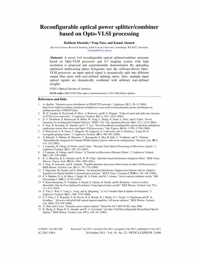
Introduction
Recently, reconfigurable optical power splitters/combiners have attracted much attention due
to the rapid deployment of passive optical networks (PON) for fiber-to-the-premises (FTTP),
optical metropolitan area networks (MAN), and active optical cables for TV/video signal
transport and distribution [1]. Currently, passive optical splitters/combiners are used in PONs
where several hundred users share one optical line terminal (OLT) at the central office,
distributing optical power to several tens of optical network units (ONUs) at the customer
end of the network, each of which is shared by many users [2]. However, passive optical
power splitters/combiners have limitations, not only in adding/dropping users to/from an
ONU but also in changing services for each user [3–6]. A reconfigurable optical power
splitter/combiner can dynamically distribute/combine the optical power and services to/from
users in the entire optical access network, thus providing numerous advantages such as
improvement of optical network efficiency and network scalability, and high network
reliability.
Another possible application of reconfigurable optical splitters/combiners is in the area of
photonic signal processing [7, 8], where lightweight and broadband are of prime concern [9–
11]. A reconfigurable optical splitter/combiner provides RF photonic systems with the
capability of dynamically changing the weights of optical signals leading to adaptive signal
processing.
Not many dynamic optical splitter/combiner structures have previously been reported [12,
13], and none of the reported dynamic optical splitter structures [14–18] have demonstrated
the capability of combing optical beams dynamically. In particular, the proof-of-principle
1×2 adaptive optical splitter based on Opto-VLSI processor reported by the authors [18] has
low resolution and limited output port counts due to the difficulty in controlling the beam
waist.
In this paper, we propose a novel reconfigurable optical splitter/combiner structure
employing an Opto-VLSI processor and a 4-f imaging system with an optimized optical
beam waist profile, enabling high-resolution optical power splitting to a larger number of
output optical ports. The new adaptive optical splitter/combiner has additional advantages
including (i) both optical signal splitting and combining are achieved through software using
the same structure, (ii) high diffraction efficiency (i.e. lower optical loss) as more pixels are
covered by the input optical beams, (iii) low inter-port crosstalk, (iv) simple user interface,
and (v) compressed hardware and compact packaging. A computer program was especially
developed to drive the Opto-VLSI processor and generate the desired phase holograms that
split an input signal arbitrarily and accurately to multiple output optical fiber ports, and also
combine multiple input signals with arbitrary weights into a single output optical fiber port.
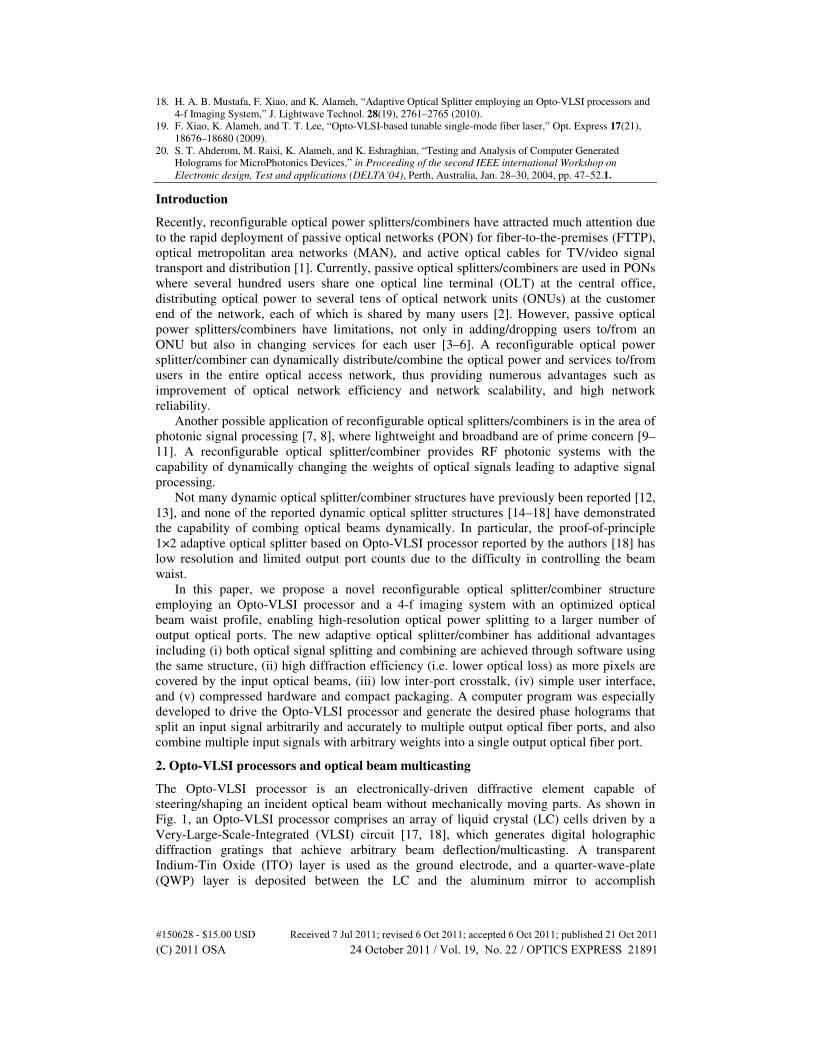
2. Opto-VLSI processors and optical beam multicasting
The Opto-VLSI processor is an electronically-driven diffractive element capable of
steering/shaping an incident optical beam without mechanically moving parts. As shown in
Fig. 1, an Opto-VLSI processor comprises an array of liquid crystal (LC) cells driven by a
Very-Large-Scale-Integrated (VLSI) circuit [17, 18], which generates digital holographic
diffraction gratings that achieve arbitrary beam deflection/multicasting. A transparent
Indium-Tin Oxide (ITO) layer is used as the ground electrode, and a quarter-wave-plate
(QWP) layer is deposited between the LC and the aluminum mirror to accomplish
#150628 - $15.00 USD Received 7 Jul 2011; revised 6 Oct 2011; accepted 6 Oct 2011; published 21 Oct 2011(C) 2011 OSA 24 October 2011 / Vol. 19, No. 22 / OPTICS EXPRESS 21891
polarization-insensitive operation. The voltage level of each pixel can individually be
controlled by using a few memory elements that select a discrete voltage level and apply it,
through the electrodes, across the LC cell.
A multicasting phase hologram can split an incident optical beam to N output beams with
variable intensities in different directions, as illustrated in Fig. 1. A collimated beam incident
onto the Opto-VLSI processor is diffracted along different directions, where the power of
each diffracted beam depends on the multicasting phase hologram. The beam multicasting
resolution, or minimum splitting angle relative to the zeroth order diffraction beam, is given
by [19]
arcsinN d
λα
=
× (1)
where λ is the optical wavelength, N denotes the number of pixels illuminated by the incident
optical beam, and d is the pixel pitch.
Several computer algorithms, such as the genetic, simulated annealing, phase encoding,
and projection algorithms [20], have been used for generating optimized multicasting phase
holograms that produce a target far-field distribution, defined by the replay beam positions
and the corresponding power splitting ratios. For a target multicasting profile, an optimised
phase hologram can always be synthesized, which minimizes the 0th
order diffraction and the
crosstalk at every output port.
Fig. 1. The top figure illustrates the capability of the Opto-VLSI processor to perform optical
beam multicasting through phased holograms. The bottom figure illustrates the phase
modulation of the light through the application of voltage across the liquid crystal cells.
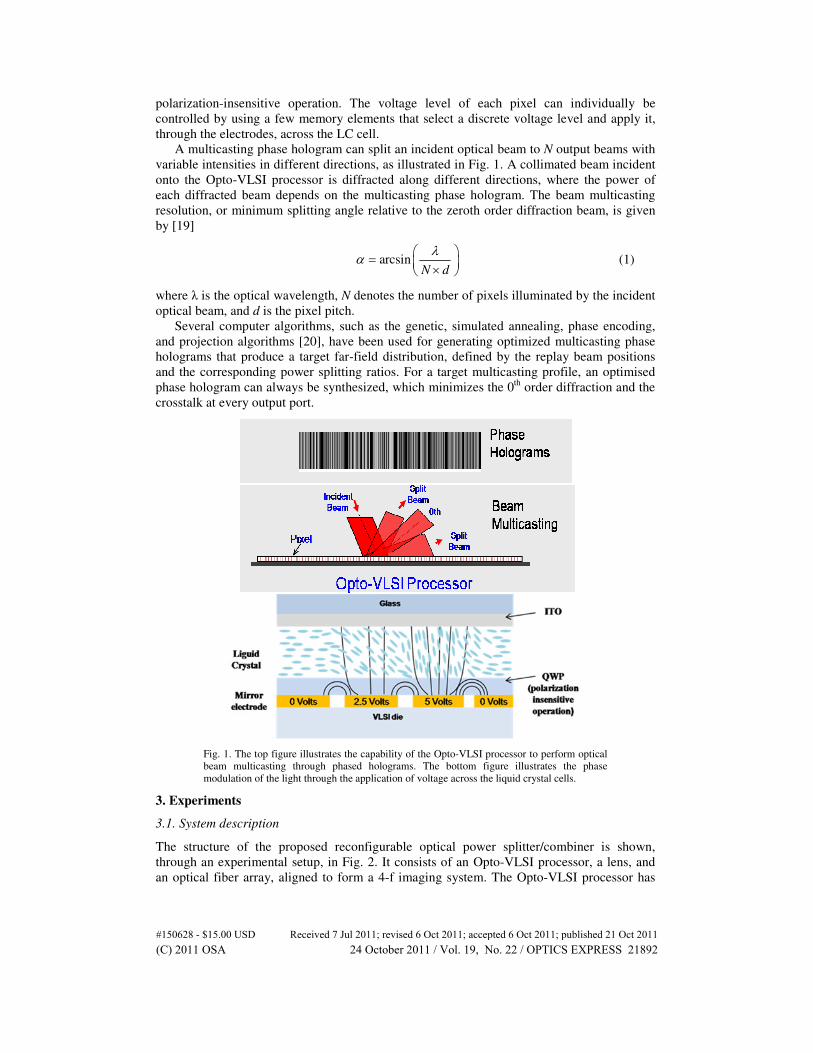
3. Experiments
3.1. System description
The structure of the proposed reconfigurable optical power splitter/combiner is shown,
through an experimental setup, in Fig. 2. It consists of an Opto-VLSI processor, a lens, and
an optical fiber array, aligned to form a 4-f imaging system. The Opto-VLSI processor has
#150628 - $15.00 USD Received 7 Jul 2011; revised 6 Oct 2011; accepted 6 Oct 2011; published 21 Oct 2011(C) 2011 OSA 24 October 2011 / Vol. 19, No. 22 / OPTICS EXPRESS 21892
1×4096 pixels with pixel size of 1.0 µm wide and 6.0 mm length, and 1.8µm pixel pitch (i.e.
0.8 µm of dead space between pixels). To demonstrate the 1×4 adaptive optical splitter, a
custom-made fiber array with spacing 127 µm was used. The spacing between the output
ports was 254 µm (twice of the fiber array spacing), thus the split beam angles were θ =
±0.58, ±1.16 with respect to 0th
order beam direction, as illustrated in Fig. 2. The power of
the 0th
order beam was coupled to a fiber port for monitoring the diffraction efficiency of the
Opto-VLSI processor.
A 1550 nm laser source with an output optical power of +1.5 dBm was used as the input
signal, and launched through the input port of the splitter. A lens of focal length f = 25 mm
was placed between and at an equal distance, f, from both the fiber array and the Opto-VLSI
processor. With no phase hologram uploaded onto the Opto-VLSI processor, only the 0th
order diffraction beam was reflected back and focused through the imaging system into same
fiber input port 5 centered the four output fiber ports, resulting in minimum crosstalk into
ports 2, and 3, as illustrated in Fig. 2. The 0th
order signal was directed to optical spectrum
analyzers (OSA), via a circulator, in order to monitor the diffraction efficiency. The input
signal from the input port at the fiber array was collimated through a lens, to an optical beam
diameter of 5.48 mm, which illuminated around 3046 pixels of the Opto-VLSI processor,
leading to a high diffraction efficiency and high optical splitting resolution of 0.01 degree
(around 10 times better than the resolution reported in [18]).
Splitter
(b)
Combiner
(c)
Port 1
Port 2
Port 3
Port 4
Port 51
2
3
Op
to-V
LS
I p
roce
sso
r
Fiber array
Imaging
lens
Polarization
controller
4
Optical combiner inputs
Optical combiner
output
ff
Op
tica
l s
plitt
er
ou
tpu
ts
1 2 3 4
Optical Splitter input Circulator
(a)
1
32
Fig. 2. (a) Schematic diagram of the reconfigurable optical splitter/combiner using an Opto-
VLSI processor and a 4-f imaging systems. (b) and (c) Optical beam propagation for splitting
and combining modes, respectively.
By driving the Opto-VLSI processor with an optimized multicasting phase hologram, the
optical beam illuminating the Opto-VLSI processor was split into four different optical
#150628 - $15.00 USD Received 7 Jul 2011; revised 6 Oct 2011; accepted 6 Oct 2011; published 21 Oct 2011(C) 2011 OSA 24 October 2011 / Vol. 19, No. 22 / OPTICS EXPRESS 21893
beams (in addition to the 0th
order beam) which propagated along the optimized directions so
that they were coupled back into the fiber output ports through the 4-f imaging system. The
split optical beams coupled into the output ports propagated along angles equal to
2,30.58θ = ± ° , and
1,41.16θ = ± ° with respect to the 0
th order beam direction. Optical
spectrum analyzers (OSA) were used to monitor the power levels of the split optical signals
coupled into the output ports 1, 2, 3 and 4.
To demonstrate the principle of the reconfigurable optical combiner, four optical signals
of equal power levels (−5.7dBm) were launched into Ports 1, 2, 3 and 4 as in Fig. 2, and,
through a multicasting phase hologram, combined into Port 5, which was monitored using an
optical spectrum analyzer. As will be discussed subsequently, a multicasting phase hologram
uploaded onto the Opto-VLSI processor enabled the four optical signals launched into Ports
1-4 to be combined at Port 5 with a weight profile that matches the splitting profile of the
corresponding multicasting phase hologram.
3.2. Experimental Results and Discussion
Several scenarios with different splitting ratios were attempted in the experiments to
demonstrate the reconfigurable optical power splitting/combing capability of the proposed
optical splitter/combiner. Table 1 shows the measured output power levels, P1, P2, P3 and P4
of the splitter, coupled into Port 1, Port 2, Port 3 and Port 4, respectively, corresponding to
different splitting ratios (H).
As shown in Table.1, in Scenario 1 a multicasting hologram corresponds to a splitting
profile H1 = 1.0:1.0:1.0:1.0 was used, demonstrating that the input optical power is split
equally into the four output ports, resulting in uniform optical power distribution at all the
four output ports. In Scenarios 2, a splitting profile H2 = 1.0:1.0:0.01:1.0 was used, which
corresponds to the case when the output signal in Port 3 was attenuated by 20 dB. In Scenario
3, the signals coupled to Port 2 and Port 3 were switched off by uploading a phase hologram
corresponding to a splitting ratio of H3 = 1.0:0.0:0.0:1.0, respectively. The measured
crosstalk level was around −30 dB. In Scenario 4 the output optical signals coupled to Port 2
and Port 3 were attenuated by 3 dB corresponding to a splitting profile of H4 =
1.0:0.5:0.5:1.0.
Table 1. Different splitting profiles corresponding to optimised multicasting holograms
uploaded onto the Opto-VLSI processor, and the corresponding measured output optical
power levels at Ports 1-4
Splitting ratio P 1 (dBm) P 2 (dBm) P 3 (dBm) P 4 (dBm) H1 = 1.0:1.0:1.0:1.0 −13.18 −13.47 −13.37 −13.76 H2 = 1.0:1.0:0.01:1.0 −13.16 −13.47 −33.01 −12.59 H3 = 1.0:0.0:0.0:1.0 −11.87 −42.50 −43.93 −11.54 H4 = 1.0:0.5:0.5:1.0 −12.30 −16.60 −16.83 −12.10
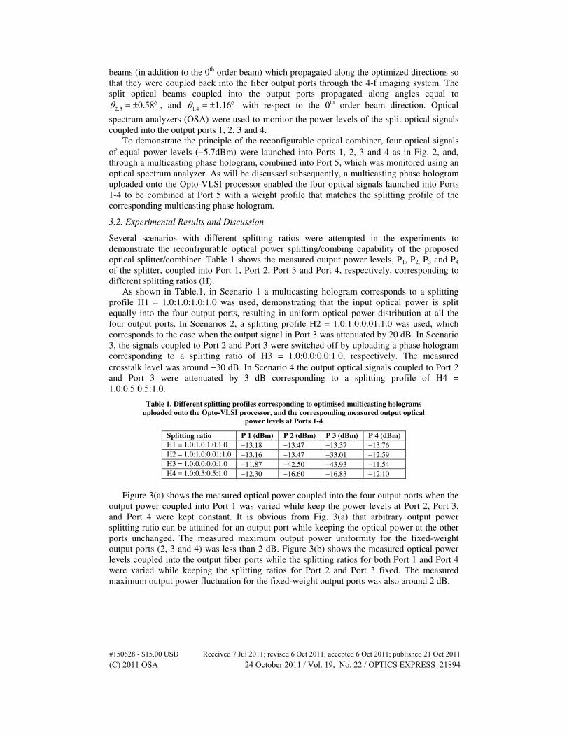
Figure 3(a) shows the measured optical power coupled into the four output ports when the
output power coupled into Port 1 was varied while keep the power levels at Port 2, Port 3,
and Port 4 were kept constant. It is obvious from Fig. 3(a) that arbitrary output power
splitting ratio can be attained for an output port while keeping the optical power at the other
ports unchanged. The measured maximum output power uniformity for the fixed-weight
output ports (2, 3 and 4) was less than 2 dB. Figure 3(b) shows the measured optical power
levels coupled into the output fiber ports while the splitting ratios for both Port 1 and Port 4
were varied while keeping the splitting ratios for Port 2 and Port 3 fixed. The measured
maximum output power fluctuation for the fixed-weight output ports was also around 2 dB.
#150628 - $15.00 USD Received 7 Jul 2011; revised 6 Oct 2011; accepted 6 Oct 2011; published 21 Oct 2011(C) 2011 OSA 24 October 2011 / Vol. 19, No. 22 / OPTICS EXPRESS 21894
-40
-35
-30
-25
-20
-15
-10
-5
0 0.2 0.4 0.6 0.8 1
Mea
sure
d o
utp
ut p
ow
er (
dB
m)
Weight of Port 1
(a)
Port 1
Port 2
Port 3
Port 4
-24
-22
-20
-18
-16
-14
-12
-10
0 0.2 0.4 0.6 0.8 1
Mea
sure
d o
utp
ut p
ow
er (
dB
m)
Weight of Port 1/Port 4
(b)
Port 1
Port 2
Port 3
Port 4
Fig. 3. (a) Measured optical power coupled into the output fiber Ports when varying the
weight of Port 1 while keeping the splitting ratios for others output fiber ports constant. (b)
Measured optical power coupled into the output fiber Ports when varying the weights of Port
1and Port 4 while keeping the splitting ratios for Port 2 and Port 3 weights unchanged.
-50
-45
-40
-35
-30
-25
-20
-15
-10
1525 1535 1545 1555 1565 1575
Mea
sure
d o
utp
ut
op
tica
l pow
er (
dB
m)
Wavelength (nm)
(a)
-50
-45
-40
-35
-30
-25
-20
-15
-10
1525 1535 1545 1555 1565 1575
Mea
sure
d o
utp
ut
op
tica
l pow
er (
dB
m)
Wavelength (nm)
(b)
-50
-45
-40
-35
-30
-25
-20
-15
-10
1525 1535 1545 1555 1565 1575
Mea
sure
d o
utp
ut
opti
cal
pow
er (
dB
m)
Wavelength (nm)
(c)
-50
-45
-40
-35
-30
-25
-20
-15
-10
1525 1535 1545 1555 1565 1575
Mea
sure
d o
utp
ut
opti
cal
pow
er (
dB
m)
Wavelength (nm)
(d)
Fig. 4. Input signals launched into Ports 1, 2, 3, and 4, and output combined optical signal at
Port 5 for phase holograms corresponding to splitting ratios of (a) 1.0:1.0:1.0:1.0, (b)
1.0:1.0:0.01:1.0, (c) 1.0:0.0:0.0:1.0 and (d) 1.0:0.5:0.5:1.0.
#150628 - $15.00 USD Received 7 Jul 2011; revised 6 Oct 2011; accepted 6 Oct 2011; published 21 Oct 2011(C) 2011 OSA 24 October 2011 / Vol. 19, No. 22 / OPTICS EXPRESS 21895
Figures 3(a, b) demonstrates the ability of the reconfigurable optical splitter structure to
realize arbitrary optical splitting ratios through the use of optimized multicasting phase
holograms.
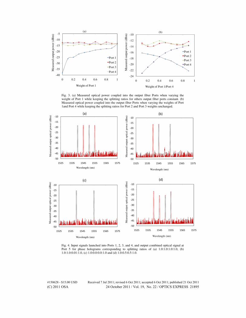
The principle of the reconfigurable optical combiner was demonstrated by launching four
input signals into Ports 1, 2, 3 and 4 and measuring the output signal from Port 5. Figures
4(a-d) show the output combined optical signal at Port 5 for the same phase holograms used
in Table.1, which correspond to combining profiles of 1.0:1.0:1.0:1.0, 1.0:1.0:0.01:1.0,
1.0:0.0:0.0:1.0 and 1.0:0.5:0.5:1.0, respectively. Note that in Fig. 4(d) the power levels of the
two center channels are actually around 4 dB below those of the outside channels, as evident
from Table 1, row 4. The discrepancy between theory and experimental measurements is
attributed to measurement errors. Figures 4(a-d) demonstrates the ability of the Opto-VLSI
processor to combine the input optical signals with an arbitrarily weight profile and couple
them into the output fiber Port 5.
Figures 3 and 4 demonstrate the ability of the reconfigurable optical splitter/combiner
structure to realize arbitrary optical splitting/combining ratios through the use of optimized
multicasting phase holograms. The measured output power splitting/combining ratios are in
excellent agreement with the user defined ratios. Note that the crosstalk for dynamic
splitting/combining is around −30 dB.
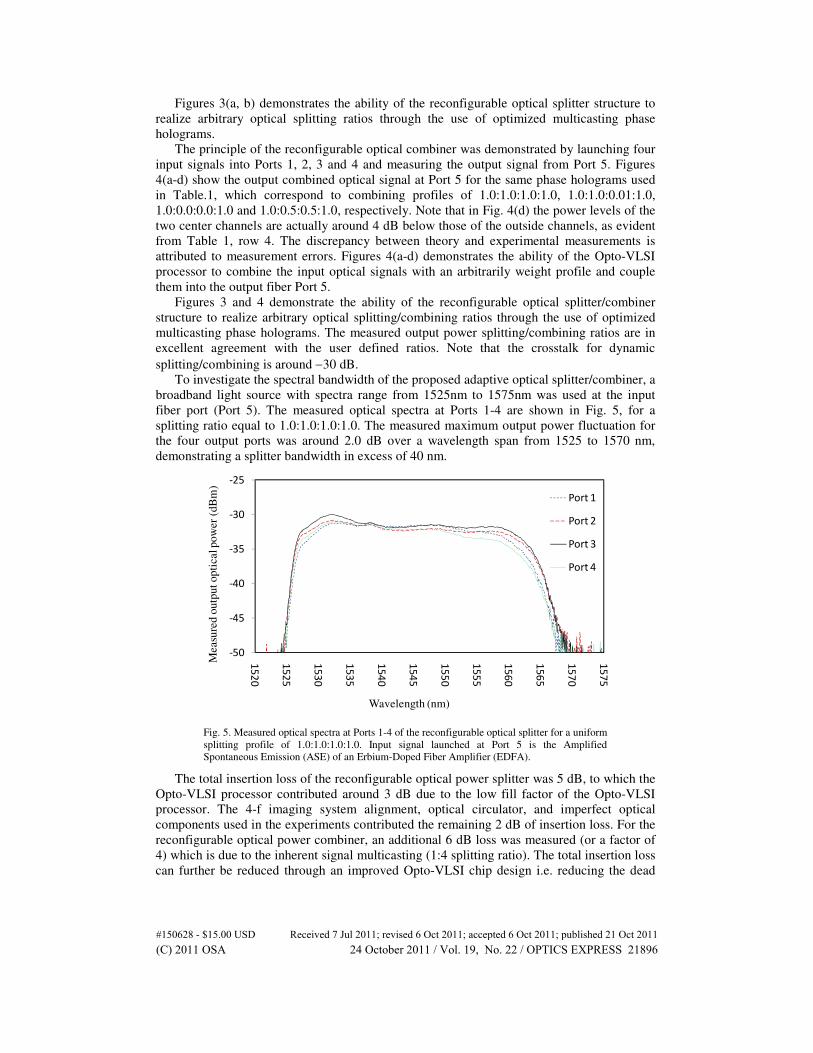
To investigate the spectral bandwidth of the proposed adaptive optical splitter/combiner, a
broadband light source with spectra range from 1525nm to 1575nm was used at the input
fiber port (Port 5). The measured optical spectra at Ports 1-4 are shown in Fig. 5, for a
splitting ratio equal to 1.0:1.0:1.0:1.0. The measured maximum output power fluctuation for
the four output ports was around 2.0 dB over a wavelength span from 1525 to 1570 nm,
demonstrating a splitter bandwidth in excess of 40 nm.
-50
-45
-40
-35
-30
-25
15
20
15
25
15
30
15
35
15
40
15
45
15
50
15
55
15
60
15
65
15
70
15
75
Measu
red o
utp
ut op
tical p
ow
er
(dB
m)
Wavelength (nm)
Port 1
Port 2
Port 3
Port 4
Fig. 5. Measured optical spectra at Ports 1-4 of the reconfigurable optical splitter for a uniform
splitting profile of 1.0:1.0:1.0:1.0. Input signal launched at Port 5 is the Amplified
Spontaneous Emission (ASE) of an Erbium-Doped Fiber Amplifier (EDFA).
The total insertion loss of the reconfigurable optical power splitter was 5 dB, to which the
Opto-VLSI processor contributed around 3 dB due to the low fill factor of the Opto-VLSI
processor. The 4-f imaging system alignment, optical circulator, and imperfect optical
components used in the experiments contributed the remaining 2 dB of insertion loss. For the
reconfigurable optical power combiner, an additional 6 dB loss was measured (or a factor of
4) which is due to the inherent signal multicasting (1:4 splitting ratio). The total insertion loss
can further be reduced through an improved Opto-VLSI chip design i.e. reducing the dead
#150628 - $15.00 USD Received 7 Jul 2011; revised 6 Oct 2011; accepted 6 Oct 2011; published 21 Oct 2011(C) 2011 OSA 24 October 2011 / Vol. 19, No. 22 / OPTICS EXPRESS 21896
area between pixels to below 0.25 micron, and the use of broadband AR coatings for the
various optical components.
4. Conclusion
A 1×4 reconfigurable optical splitter/combiner structure employing an Opto-VLSI processor
in conjunction with a 4-f imaging system has been demonstrated. Experimental results have
shown that an input optical signal can arbitrarily be split and coupled into four output optical
fiber ports by simply uploading optimized multicasting phase holograms onto the Opto-VLSI
processor. The experimental results have also demonstrated that four input optical signals can
dynamically be combined with arbitrary weights into a single optical fiber port. A crosstalk
level below −30 dB and a wavelength range exceeding 40 nm have experimentally been
measured, making the reconfigurable optical splitter/combiner attractive for access optical
networks and optical signal processing.
Acknowledgment
We acknowledge the support of the Faculty of Computing, health and Science, Edith Cowan
University, Department of Nanobio Materials and Electronics, Gwangju Institute of science
and Technology, Korea, and the State Key Laboratory of Advanced Optical Communication
Systems and Networks, China.
#150628 - $15.00 USD Received 7 Jul 2011; revised 6 Oct 2011; accepted 6 Oct 2011; published 21 Oct 2011(C) 2011 OSA 24 October 2011 / Vol. 19, No. 22 / OPTICS EXPRESS 21897