LI ET AL. VOL. 5 ’ NO. 9 ’ 6955–6961 ’ 2011 www.acsnano.org 6955 August 11, 2011 C 2011 American Chemical Society Reduced Graphene Oxide Electrically Contacted Graphene Sensor for Highly Sensitive Nitric Oxide Detection Weiwei Li, † Xiumei Geng, † Yufen Guo, † Jizan Rong, † Youpin Gong, † Liqiong Wu, † Xuemin Zhang, † Peng Li, † Jianbao Xu, † Guosheng Cheng, † Mengtao Sun, ‡ and Liwei Liu †, * † Suzhou Institute of Nano-Tech and Nano-Bionics, Chinese Academy of Sciences, Suzhou 215123, People's Republic of China and ‡ Institute of Physics, Chinese Academy of Sciences, Beijing 100190, People's Republic of China G raphene is a single atomic layer of sp 2 -carbon atoms with two-dimen- sional hexagonal crystal structure. Large speci fic surface area and high carrier mobility enable graphene to be a promising application in electricity-based sensors. 1 Graphene-based field-effect tran- sistors (FETs) have been examined using mechanical exfoliated graphene as a sensi- tive channel, exhibiting the sensing ability of individual NO 2 gas molecules. 2 Com- pared with chemically inert graphene, 24 reduced graphene oxide (RGO) being of active sites and function groups has been widely demonstrated to be able to detect NO 2 , 5,6 NH 3 , 5 H 2 7,8 and organic vapors. 9,10 Efforts have been ongoing to focus on the effects of chemical decoration, reduction degree, and device fabrication of RGO on selectivity, sensitivity, and recovery prop- erties of detector devices. 7,10 There is plenty of room for exploration and improve- ment in this emerging field of graphene- based sensors. Nitric oxide (NO) detection plays an es- sential role in medical applications for its biological functions as a messenger mole- cule. NO molecules can mediate many bod- ily functions acting as a neurotransmitter and relaxing blood vessels. The human ex- haled NO level in 2 weeks prior to outbreak of asthma is doubly elevated compared to everyday NO level of 716 ppb, 11 and the detection of NO is critical for an asthma patient in a hospital and with household monitoring. Despite the elevation before outbreak, the NO concentration is still with- in a range of a few tens of parts per billion. Thus, highly sensitive and portable detec- tion of NO is urgently required for asthma patients. Carbon nanotubes (CNTs) have been ex- plored to sense NO gas. 1115 Star et al. developed a functionalized CNT network sensor to detect NO gas indirectly by con- verting NO to NO 2 with CrO 3 , and the direct detection of NO in such devices showed poor performance due to the weak electron donor nature of NO and the detection abil- ity of CNT network devices. 11 Emerging graphene has attracted increasing attention for detection of NO molecules; furthermore, electrons transfer from NO to graphene, and the weak binding between NO molecules and graphene has been recognized theo- retically. 16,17 By contrast with single-walled carbon nanotubes (SWNTs), RGO is readily prepared in large quantities and is well- dispersed in aqueous solution without ad- ditional surfactants. Thus, it is significant for both fundamental study and application to explore RGO for the direct detection of NO. However, to our best knowledge, related experimental work about direct sensing NO molecules using graphene-based devices has not been reported so far. As for device fabrications of carbon nano- materials, alternating current dielectrophor- esis (ac-DEP) provides a simple, scalable, and low-cost method to trap carbon nano- tubes and graphene for making elec- tronic devices. 1822 However, an important * Address correspondence to [email protected]. Received for review April 18, 2011 and accepted August 11, 2011. Published online 10.1021/nn201433r ABSTRACT We develop graphene-based devices fabricated by alternating current dielectrophor- esis (ac-DEP) for highly sensitive nitric oxide (NO) gas detection. The novel device comprises the sensitive channels of palladium-decorated reduced graphene oxide (Pd-RGO) and the electrodes covered with chemical vapor deposition (CVD)-grown graphene. The highly sensitive, recoverable, and reliable detection of NO gas ranging from 2 to 420 ppb with response time of several hundred seconds has been achieved at room temperature. The facile and scalable route for high performance suggests a promising application of graphene devices toward the human exhaled NO and environmental pollutant detections. KEYWORDS: graphene . nitric oxide . dielectrophoresis . reduced graphene oxide . highly sensitive ARTICLE
Jianbao Xu,† Guosheng Cheng,† Mengtao Sun,‡ and Liwei Liu†,*
†Suzhou Institute of Nano-Tech and Nano-Bionics, Chinese Academy of Sciences, Suzhou 215123, People's Republic of China and ‡Institute of Physics, ChineseAcademy of Sciences, Beijing 100190, People's Republic of China
Graphene is a single atomic layer ofsp2-carbon atoms with two-dimen-sional hexagonal crystal structure.
Large specific surface area and highcarrier mobility enable graphene to be apromising application in electricity-basedsensors.1 Graphene-based field-effect tran-sistors (FETs) have been examined usingmechanical exfoliated graphene as a sensi-tive channel, exhibiting the sensing abilityof individual NO2 gas molecules.2 Com-pared with chemically inert graphene,2�4
reduced graphene oxide (RGO) being ofactive sites and function groups has beenwidely demonstrated to be able to detectNO2,
5,6 NH3,5 H2
7,8 and organic vapors.9,10
Efforts have been ongoing to focus on theeffects of chemical decoration, reductiondegree, and device fabrication of RGO onselectivity, sensitivity, and recovery prop-erties of detector devices.7,10 There isplenty of room for exploration and improve-ment in this emerging field of graphene-based sensors.Nitric oxide (NO) detection plays an es-
sential role in medical applications for itsbiological functions as a messenger mole-cule. NO molecules can mediate many bod-ily functions acting as a neurotransmitterand relaxing blood vessels. The human ex-haled NO level in 2 weeks prior to outbreakof asthma is doubly elevated compared toeveryday NO level of 7�16 ppb,11 and thedetection of NO is critical for an asthmapatient in a hospital and with householdmonitoring. Despite the elevation beforeoutbreak, the NO concentration is still with-in a range of a few tens of parts per billion.Thus, highly sensitive and portable detec-tion of NO is urgently required for asthmapatients.Carbon nanotubes (CNTs) have been ex-
plored to sense NO gas.11�15 Star et al.
developed a functionalized CNT networksensor to detect NO gas indirectly by con-verting NO to NO2 with CrO3, and the directdetection of NO in such devices showedpoor performance due to the weak electrondonor nature of NO and the detection abil-ity of CNT network devices.11 Emerginggraphene has attracted increasing attentionfor detection of NOmolecules; furthermore,electrons transfer fromNO to graphene, andthe weak binding between NO moleculesand graphene has been recognized theo-retically.16,17 By contrast with single-walledcarbon nanotubes (SWNTs), RGO is readilyprepared in large quantities and is well-dispersed in aqueous solution without ad-ditional surfactants. Thus, it is significant forboth fundamental study and application toexplore RGO for the direct detection of NO.However, to our best knowledge, relatedexperimental work about direct sensing NOmolecules using graphene-based deviceshas not been reported so far.As for device fabrications of carbon nano-
materials, alternating current dielectrophor-esis (ac-DEP) provides a simple, scalable, andlow-cost method to trap carbon nano-tubes and graphene for making elec-tronic devices.18�22 However, an important
drawback of such devices derived from ac-DEP lies inthe poor electrical contacts, which result in high resis-tance betweenmetal electrodes and nanoscale carbonmaterials owing to sample-on-electrode configuration,as well as the presence of Schottky barriers or residuesurfactants.23
Here, we fabricate the NO sensor devices usingac-DEP of the palladium-decorated reduced gra-phene oxide (Pd-RGO) nanosheets with chemicalvapor deposition (CVD)-grown graphene electrodes.The highly sensitive, recoverable, and reliable detec-tion of NO gas ranging from 2 to 420 ppb withresponse time of several hundred seconds has beenachieved. We adopt a bulk-phase Pd nanoparticle(NP) decoration of RGO as active channels by asolution chemistry method instead of previouslyreported Pd NPs merely on the surface of the gra-phene-based devices by electrochemical or physicaldeposition.7,8 The advantages of Pd decoration andCVD-grown graphene contacts of RGO in improvingthe sensitivity and stability of NO sensors have beenrevealed by performing comparison experiments ofvarious devices. Highly sensitive graphene-basedsensor toward directly detecting nitric oxide (NO) isa very promising application for monitoring respira-tory disorders and sensing air pollutants.
RESULTS AND DISCUSSION
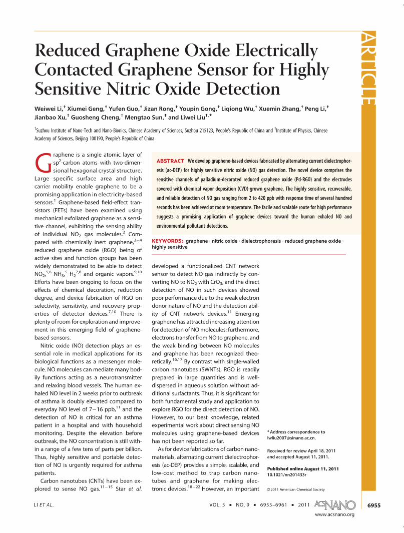
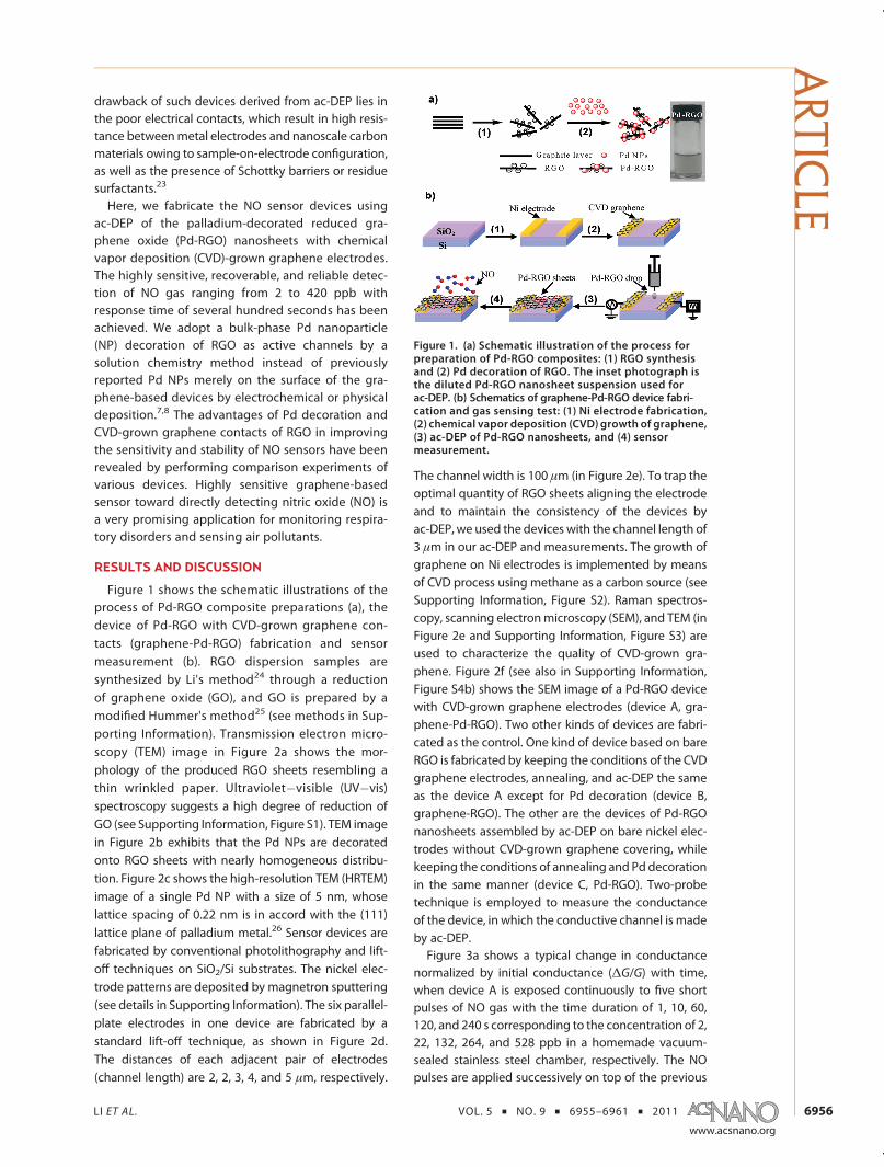
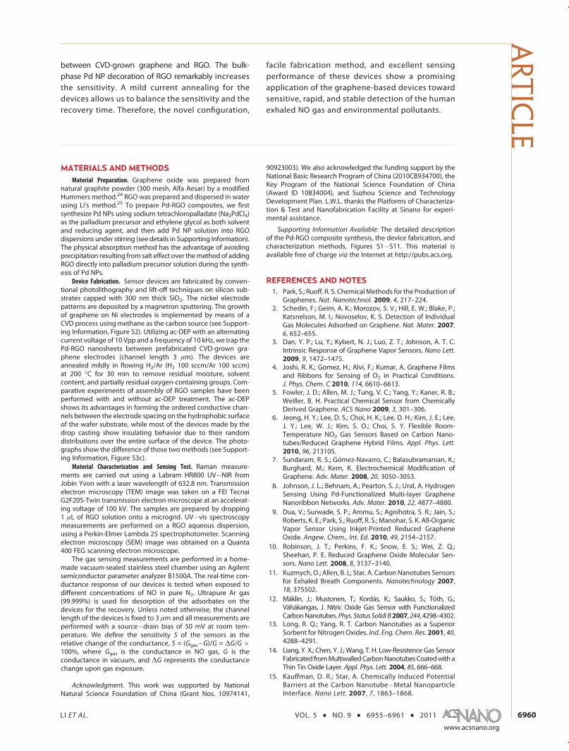
Figure 1 shows the schematic illustrations of theprocess of Pd-RGO composite preparations (a), thedevice of Pd-RGO with CVD-grown graphene con-tacts (graphene-Pd-RGO) fabrication and sensormeasurement (b). RGO dispersion samples aresynthesized by Li's method24 through a reductionof graphene oxide (GO), and GO is prepared by amodified Hummer's method25 (see methods in Sup-porting Information). Transmission electron micro-scopy (TEM) image in Figure 2a shows the mor-phology of the produced RGO sheets resembling athin wrinkled paper. Ultraviolet�visible (UV�vis)spectroscopy suggests a high degree of reduction ofGO (see Supporting Information, Figure S1). TEM imagein Figure 2b exhibits that the Pd NPs are decoratedonto RGO sheets with nearly homogeneous distribu-tion. Figure 2c shows the high-resolution TEM (HRTEM)image of a single Pd NP with a size of 5 nm, whoselattice spacing of 0.22 nm is in accord with the (111)lattice plane of palladium metal.26 Sensor devices arefabricated by conventional photolithography and lift-off techniques on SiO2/Si substrates. The nickel elec-trode patterns are deposited by magnetron sputtering(see details in Supporting Information). The six parallel-plate electrodes in one device are fabricated by astandard lift-off technique, as shown in Figure 2d.The distances of each adjacent pair of electrodes(channel length) are 2, 2, 3, 4, and 5 μm, respectively.
The channel width is 100 μm (in Figure 2e). To trap theoptimal quantity of RGO sheets aligning the electrodeand to maintain the consistency of the devices byac-DEP, we used the devices with the channel length of3 μm in our ac-DEP and measurements. The growth ofgraphene on Ni electrodes is implemented by meansof CVD process using methane as a carbon source (seeSupporting Information, Figure S2). Raman spectros-copy, scanning electronmicroscopy (SEM), and TEM (inFigure 2e and Supporting Information, Figure S3) areused to characterize the quality of CVD-grown gra-phene. Figure 2f (see also in Supporting Information,Figure S4b) shows the SEM image of a Pd-RGO devicewith CVD-grown graphene electrodes (device A, gra-phene-Pd-RGO). Two other kinds of devices are fabri-cated as the control. One kind of device based on bareRGO is fabricated by keeping the conditions of the CVDgraphene electrodes, annealing, and ac-DEP the sameas the device A except for Pd decoration (device B,graphene-RGO). The other are the devices of Pd-RGOnanosheets assembled by ac-DEP on bare nickel elec-trodes without CVD-grown graphene covering, whilekeeping the conditions of annealing and Pddecorationin the same manner (device C, Pd-RGO). Two-probetechnique is employed to measure the conductanceof the device, in which the conductive channel is madeby ac-DEP.Figure 3a shows a typical change in conductance
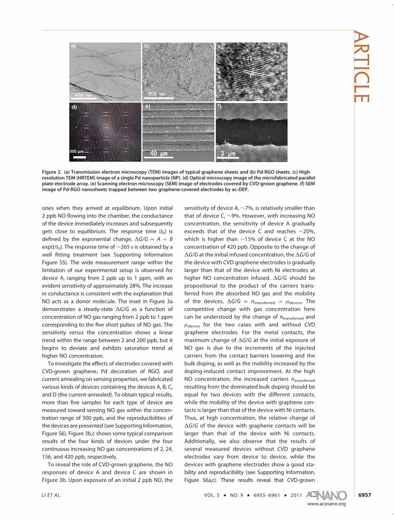
normalized by initial conductance (ΔG/G) with time,when device A is exposed continuously to five shortpulses of NO gas with the time duration of 1, 10, 60,120, and 240 s corresponding to the concentration of 2,22, 132, 264, and 528 ppb in a homemade vacuum-sealed stainless steel chamber, respectively. The NOpulses are applied successively on top of the previous
Figure 1. (a) Schematic illustration of the process forpreparation of Pd-RGO composites: (1) RGO synthesisand (2) Pd decoration of RGO. The inset photograph isthe diluted Pd-RGO nanosheet suspension used forac-DEP. (b) Schematics of graphene-Pd-RGO device fabri-cation and gas sensing test: (1) Ni electrode fabrication,(2) chemical vapor deposition (CVD) growth of graphene,(3) ac-DEP of Pd-RGO nanosheets, and (4) sensormeasurement.
ARTIC
LE
LI ET AL. VOL. 5 ’ NO. 9 ’ 6955–6961 ’ 2011
www.acsnano.org
6957
ones when they arrived at equilibrium. Upon initial2 ppb NO flowing into the chamber, the conductanceof the device immediately increases and subsequentlygets close to equilibrium. The response time (t0) isdefined by the exponential change, ΔG/G � A þ B
exp(t/t0). The response time of∼265 s is obtained by awell fitting treatment (see Supporting InformationFigure S5). The wide measurement range within thelimitation of our experimental setup is observed fordevice A, ranging from 2 ppb up to 1 ppm, with anevident sensitivity of approximately 28%. The increasein conductance is consistent with the explanation thatNO acts as a donor molecule. The inset in Figure 3ademonstrates a steady-state ΔG/G as a function ofconcentration of NO gas ranging from 2 ppb to 1 ppmcorresponding to the five short pulses of NO gas. Thesensitivity versus the concentration shows a lineartrend within the range between 2 and 200 ppb, but itbegins to deviate and exhibits saturation trend athigher NO concentration.To investigate the effects of electrodes covered with
CVD-grown graphene, Pd decoration of RGO, andcurrent annealing on sensing properties, we fabricatedvarious kinds of devices containing the devices A, B, C,and D (the current-annealed). To obtain typical results,more than five samples for each type of device aremeasured toward sensing NO gas within the concen-tration range of 500 ppb, and the reproducibilities ofthe devices are presented (see Supporting Information,Figure S6). Figure 3b,c shows some typical comparisonresults of the four kinds of devices under the fourcontinuous increasing NO gas concentrations of 2, 24,156, and 420 ppb, respectively.To reveal the role of CVD-grown graphene, the NO
responses of device A and device C are shown inFigure 3b. Upon exposure of an initial 2 ppb NO, the
sensitivity of device A, ∼7%, is relatively smaller thanthat of device C, ∼9%. However, with increasing NOconcentration, the sensitivity of device A graduallyexceeds that of the device C and reaches ∼20%,which is higher than ∼15% of device C at the NOconcentration of 420 ppb. Opposite to the change ofΔG/G at the initial infused concentration, theΔG/G ofthe device with CVD graphene electrodes is graduallylarger than that of the device with Ni electrodes athigher NO concentration infused. ΔG/G should bepropositional to the product of the carriers trans-ferred from the absorbed NO gas and the mobilityof the devices, ΔG/G � ntransferred � μdevice. Thecompetitive change with gas concentration herecan be understood by the change of ntransferred andμdevice for the two cases with and without CVDgraphene electrodes. For the metal contacts, themaximum change of ΔG/G at the initial exposure ofNO gas is due to the increments of the injectedcarriers from the contact barriers lowering and thebulk doping, as well as the mobility increased by thedoping-induced contact improvement. At the highNO concentration, the increased carriers ntransferredresulting from the dominated bulk doping should beequal for two devices with the different contacts,while the mobility of the device with graphene con-tacts is larger than that of the device with Ni contacts.Thus, at high concentration, the relative change ofΔG/G of the device with graphene contacts will belarger than that of the device with Ni contacts.Additionally, we also observe that the results ofseveral measured devices without CVD grapheneelectrodes vary from device to device, while thedevices with graphene electrodes show a good sta-bility and reproducibility (see Supporting Information,Figure S6a,c). These results reveal that CVD-grown
Figure 2. (a) Transmission electron microscopy (TEM) images of typical graphene sheets and (b) Pd-RGO sheets. (c) High-resolution TEM (HRTEM) image of a single Pd nanoparticle (NP). (d) Optical microscopy image of the microfabricated parallelplate electrode array. (e) Scanning electron microscopy (SEM) image of electrodes covered by CVD-grown graphene. (f) SEMimage of Pd-RGO nanosheets trapped between two graphene-covered electrodes by ac-DEP.
ARTIC
LE
LI ET AL. VOL. 5 ’ NO. 9 ’ 6955–6961 ’ 2011
www.acsnano.org
6958
graphene electrodes play a critical role in improvingthe contacts of RGO nanosheets, thereby elevating
significantly the stability and consistency of devices.The degraded stability and consistency of thedevices without graphene electrodes can be attrib-uted to the geometry configuration of the Pd-RGOnanosheets on Ni electrodes made by ac-DEP. Theinitial higher sensitivity for stable devices withoutgraphene electrodes can be understood consideringthe presence of the larger Schottky barriers betweenNiand Pd-RGO than that between graphene and Pd-RGOdue to the difference of work functions. The relativechange in conductance is raised by the reduction ofthe thickness of Schottky barriers at the very beginningof exposure to NO gas, where the work function of themetal electrodes is easily changed by the initial ad-sorption of gas molecules. With increasing concentra-tion of NO, the response of intrinsic bulk Pd-RGOwouldgradually dominate over the contact effect of themetalelectrodes. The scattering of the thickness-reducedbarriers is responsible for the excess sensitivity by thedevices with graphene electrodes. By contrast, theCVD-grown graphene electrodes have similar geome-try configuration and work function with RGO, result-ing in relatively trivial influence of contacts betweenCVD graphene electrodes and RGO. This contributes to
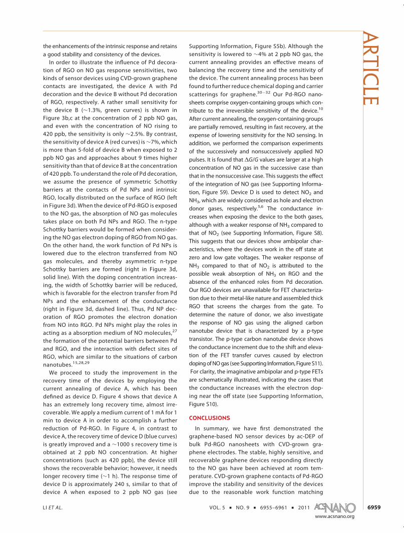
Figure 3. (a) Relative change in conductance normalizedby initial conductance (ΔG/G), real-time sensitivitydependence of device A of graphene-Pd-RGO exposed toseveral total infused NO gas molecules with the timeduration of 1, 10, 60, 120, and 240 s corresponding to theconcentrations of 2, 22, 132, 264, and 528 ppb, respec-tively. The inset demonstrates steady-state ΔG/G versusthe concentrations of total infused NO gas moleculesranging from 2 ppb to 1 ppm. (b) Typical relative changesin conductance of the various devices versus time, andthe step-shaped conductance response corresponds to 1,10, 60, and 120 s pulses of NO gas: 2, 22, 132, and 264 ppb,respectively. (c) Sensitivities versus the total infusedconcentrations of NO gas in (b). The various devices aredevice A (graphene-Pd-RGO, red curve), B (graphene-RGO, green curve), C (Pd-RGO, black curve), and D(current-annealed graphene-Pd-RGO, blue curve).(d) Schematic illustrations of the proposed mechanismfor sensitivity improvement of the devices due to the PdNP decorations of RGO. When the device of Pd-RGO wasexposed to NO gas, the original symmetric Schottkybarriers at the contacts of Pd NPs and RGO (left) aretransferred to asymmetric n-type Schottky barriers(right) for the electron doping by NO gas. With the dopingconcentration increasing, the width of the Schottkybarrier will be further reduced (right, dashed line).
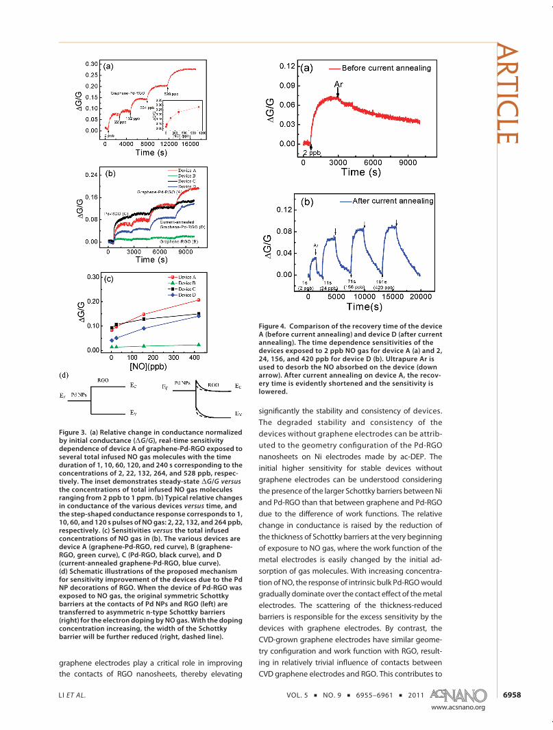
Figure 4. Comparison of the recovery time of the deviceA (before current annealing) and device D (after currentannealing). The time dependence sensitivities of thedevices exposed to 2 ppb NO gas for device A (a) and 2,24, 156, and 420 ppb for device D (b). Ultrapure Ar isused to desorb the NO absorbed on the device (downarrow). After current annealing on device A, the recov-ery time is evidently shortened and the sensitivity islowered.
ARTIC
LE
LI ET AL. VOL. 5 ’ NO. 9 ’ 6955–6961 ’ 2011
www.acsnano.org
6959
the enhancements of the intrinsic response and retainsa good stability and consistency of the devices.In order to illustrate the influence of Pd decora-
tion of RGO on NO gas response sensitivities, twokinds of sensor devices using CVD-grown graphenecontacts are investigated, the device A with Pddecoration and the device B without Pd decorationof RGO, respectively. A rather small sensitivity forthe device B (∼1.3%, green curves) is shown inFigure 3b,c at the concentration of 2 ppb NO gas,and even with the concentration of NO rising to420 ppb, the sensitivity is only ∼2.5%. By contrast,the sensitivity of device A (red curves) is∼7%, whichis more than 5-fold of device B when exposed to 2ppb NO gas and approaches about 9 times highersensitivity than that of device B at the concentrationof 420 ppb. To understand the role of Pd decoration,we assume the presence of symmetric Schottkybarriers at the contacts of Pd NPs and intrinsicRGO, locally distributed on the surface of RGO (leftin Figure 3d). When the device of Pd-RGO is exposedto the NO gas, the absorption of NO gas moleculestakes place on both Pd NPs and RGO. The n-typeSchottky barriers would be formed when consider-ing the NO gas electron doping of RGO from NO gas.On the other hand, the work function of Pd NPs islowered due to the electron transferred from NOgas molecules, and thereby asymmetric n-typeSchottky barriers are formed (right in Figure 3d,solid line). With the doping concentration increas-ing, the width of Schottky barrier will be reduced,which is favorable for the electron transfer from PdNPs and the enhancement of the conductance(right in Figure 3d, dashed line). Thus, Pd NP dec-oration of RGO promotes the electron donationfrom NO into RGO. Pd NPs might play the roles inacting as a absorption medium of NO molecules,27
the formation of the potential barriers between Pdand RGO, and the interaction with defect sites ofRGO, which are similar to the situations of carbonnanotubes.15,28,29
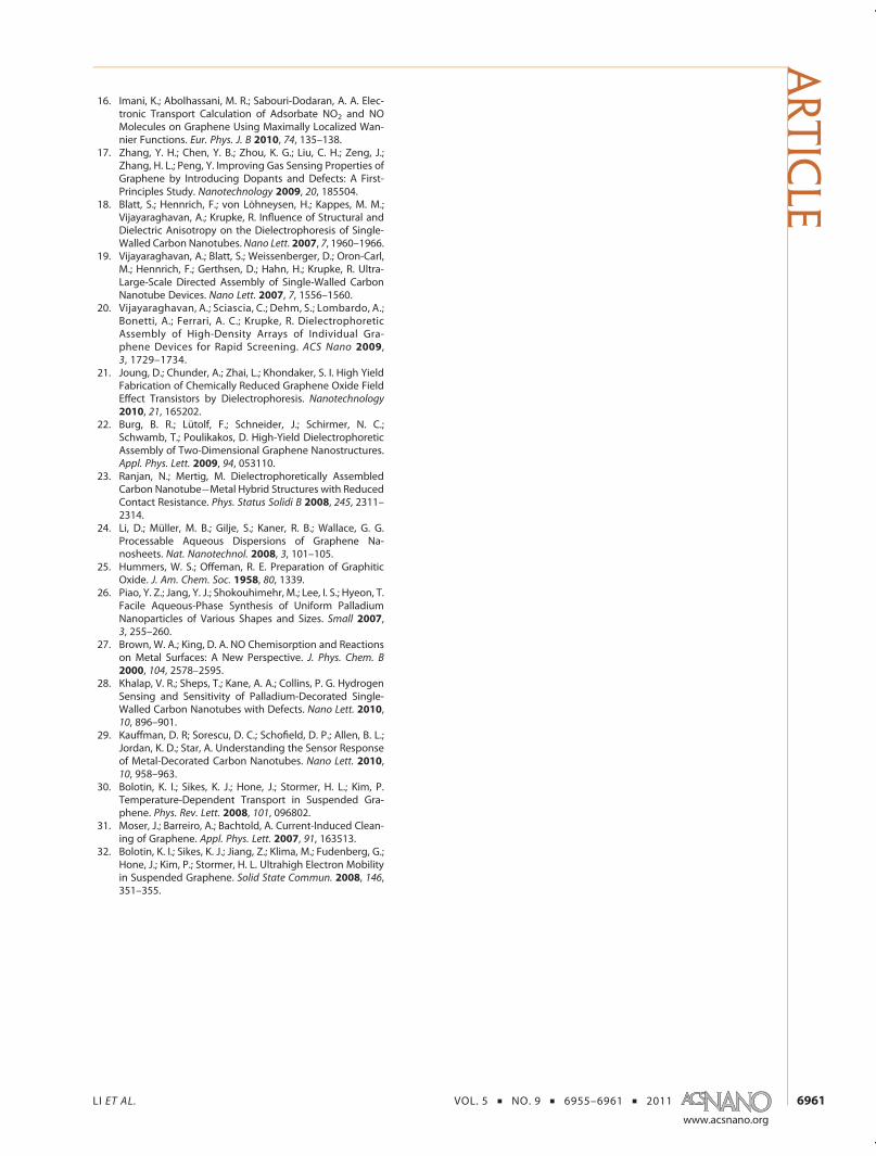
We proceed to study the improvement in therecovery time of the devices by employing thecurrent annealing of device A, which has beendefined as device D. Figure 4 shows that device Ahas an extremely long recovery time, almost irre-coverable. We apply a medium current of 1 mA for 1min to device A in order to accomplish a furtherreduction of Pd-RGO. In Figure 4, in contrast todevice A, the recovery time of device D (blue curves)is greatly improved and a ∼1000 s recovery time isobtained at 2 ppb NO concentration. At higherconcentrations (such as 420 ppb), the device stillshows the recoverable behavior; however, it needslonger recovery time (∼1 h). The response time ofdevice D is approximately 240 s, similar to that ofdevice A when exposed to 2 ppb NO gas (see
Supporting Information, Figure S5b). Although thesensitivity is lowered to ∼4% at 2 ppb NO gas, thecurrent annealing provides an effective means ofbalancing the recovery time and the sensitivity ofthe device. The current annealing process has beenfound to further reduce chemical doping and carrierscatterings for graphene.30�32 Our Pd-RGO nano-sheets comprise oxygen-containing groups which con-tribute to the irreversible sensitivity of the device.10
After current annealing, the oxygen-containing groupsare partially removed, resulting in fast recovery, at theexpense of lowering sensitivity for the NO sensing. Inaddition, we performed the comparison experimentsof the successively and nonsuccessively applied NOpulses. It is found that ΔG/G values are larger at a highconcentration of NO gas in the successive case thanthat in the nonsuccessive case. This suggests the effectof the integration of NO gas (see Supporting Informa-tion, Figure S9). Device D is used to detect NO2 andNH3, which are widely considered as hole and electrondonor gases, respectively.5,6 The conductance in-creases when exposing the device to the both gases,although with a weaker response of NH3 compared tothat of NO2 (see Supporting Information, Figure S8).This suggests that our devices show ambipolar char-acteristics, where the devices work in the off state atzero and low gate voltages. The weaker response ofNH3 compared to that of NO2 is attributed to thepossible weak absorption of NH3 on RGO and theabsence of the enhanced roles from Pd decoration.Our RGO devices are unavailable for FET characteriza-tion due to their metal-like nature and assembled thickRGO that screens the charges from the gate. Todetermine the nature of donor, we also investigatethe response of NO gas using the aligned carbonnanotube device that is characterized by a p-typetransistor. The p-type carbon nanotube device showsthe conductance increment due to the shift and eleva-tion of the FET transfer curves caused by electrondopingofNOgas (seeSupporting Information, FigureS11).For clarity, the imaginative ambipolar and p-type FETsare schematically illustrated, indicating the cases thatthe conductance increases with the electron dop-ing near the off state (see Supporting Information,Figure S10).
CONCLUSIONS
In summary, we have first demonstrated thegraphene-based NO sensor devices by ac-DEP ofbulk Pd-RGO nanosheets with CVD-grown gra-phene electrodes. The stable, highly sensitive, andrecoverable graphene devices responding directlyto the NO gas have been achieved at room tem-perature. CVD-grown graphene contacts of Pd-RGOimprove the stability and sensitivity of the devicesdue to the reasonable work function matching
ARTIC
LE
LI ET AL. VOL. 5 ’ NO. 9 ’ 6955–6961 ’ 2011
www.acsnano.org
6960
between CVD-grown graphene and RGO. The bulk-phase Pd NP decoration of RGO remarkably increasesthe sensitivity. A mild current annealing for thedevices allows us to balance the sensitivity and therecovery time. Therefore, the novel configuration,
facile fabrication method, and excellent sensingperformance of these devices show a promisingapplication of the graphene-based devices towardsensitive, rapid, and stable detection of the humanexhaled NO gas and environmental pollutants.
MATERIALS AND METHODSMaterial Preparation. Graphene oxide was prepared from
natural graphite powder (300 mesh, Alfa Aesar) by a modifiedHummers method.24 RGO was prepared and dispersed in waterusing Li's method.25 To prepare Pd-RGO composites, we firstsynthesize Pd NPs using sodium tetrachloropalladate (Na2PdCl4)as the palladium precursor and ethylene glycol as both solventand reducing agent, and then add Pd NP solution into RGOdispersions under stirring (see details in Supporting Information).The physical absorption method has the advantage of avoidingprecipitation resulting fromsalt effect over themethodof addingRGO directly into palladium precursor solution during the synth-esis of Pd NPs.
Device Fabrication. Sensor devices are fabricated by conven-tional photolithography and lift-off techniques on silicon sub-strates capped with 300 nm thick SiO2. The nickel electrodepatterns are deposited by a magnetron sputtering. The growthof graphene on Ni electrodes is implemented by means of aCVD process using methane as the carbon source (see Support-ing Information, Figure S2). Utilizing ac-DEP with an alternatingcurrent voltage of 10 Vpp and a frequency of 10 kHz, we trap thePd-RGO nanosheets between prefabricated CVD-grown gra-phene electrodes (channel length 3 μm). The devices areannealed mildly in flowing H2/Ar (H2 100 sccm/Ar 100 sccm)at 200 �C for 30 min to remove residual moisture, solventcontent, and partially residual oxygen-containing groups. Com-parative experiments of assembly of RGO samples have beenperformed with and without ac-DEP treatment. The ac-DEPshows its advantages in forming the ordered conductive chan-nels between the electrode spacing on the hydrophobic surfaceof the wafer substrate, while most of the devices made by thedrop casting show insulating behavior due to their randomdistributions over the entire surface of the device. The photo-graphs show the difference of those twomethods (see Support-ing Information, Figure S3c).
Material Characterization and Sensing Test. Raman measure-ments are carried out using a Labram HR800 UV�NIR fromJobin Yvon with a laser wavelength of 632.8 nm. Transmissionelectron microscopy (TEM) image was taken on a FEI TecnaiG2F20S-Twin transmission electron microscope at an accelerat-ing voltage of 100 kV. The samples are prepared by dropping1 μL of RGO solution onto a microgrid. UV�vis spectroscopymeasurements are performed on a RGO aqueous dispersion,using a Perkin-Elmer Lambda 25 spectrophotometer. Scanningelectron microscopy (SEM) image was obtained on a Quanta400 FEG scanning electron microscope.
The gas sensing measurements are performed in a home-made vacuum-sealed stainless steel chamber using an Agilentsemiconductor parameter analyzer B1500A. The real-time con-ductance response of our devices is tested when exposed todifferent concentrations of NO in pure N2. Ultrapure Ar gas(99.999%) is used for desorption of the adsorbates on thedevices for the recovery. Unless noted otherwise, the channellength of the devices is fixed to 3 μm and all measurements areperformed with a source�drain bias of 50 mV at room tem-perature. We define the sensitivity S of the sensors as therelative change of the conductance, S = (Ggas�G)/G = ΔG/G �100%, where Ggas is the conductance in NO gas, G is theconductance in vacuum, and ΔG represents the conductancechange upon gas exposure.
Acknowledgment. This work was supported by NationalNatural Science Foundation of China (Grant Nos. 10974141,
90923003). We also acknowledged the funding support by theNational Basic Research Program of China (2010CB934700), theKey Program of the National Science Foundation of China(Award ID 10834004), and Suzhou Science and TechnologyDevelopment Plan. L.W.L. thanks the Platforms of Characteriza-tion & Test and Nanofabrication Facility at Sinano for experi-mental assistance.
Supporting Information Available: The detailed descriptionof the Pd-RGO composite synthesis, the device fabrication, andcharacterization methods, Figures S1�S11. This material isavailable free of charge via the Internet at http://pubs.acs.org.
REFERENCES AND NOTES1. Park, S.; Ruoff, R. S. ChemicalMethods for the Production of
Graphenes. Nat. Nanotechnol. 2009, 4, 217–224.2. Schedin, F.; Geim, A. K.; Morozov, S. V.; Hill, E. W.; Blake, P.;
Katsnelson, M. I.; Novoselov, K. S. Detection of IndividualGas Molecules Adsorbed on Graphene. Nat. Mater. 2007,6, 652–655.
3. Dan, Y. P.; Lu, Y.; Kybert, N. J.; Luo, Z. T.; Johnson, A. T. C.Intrinsic Response of Graphene Vapor Sensors. Nano Lett.2009, 9, 1472–1475.
4. Joshi, R. K.; Gomez, H.; Alvi, F.; Kumar, A. Graphene Filmsand Ribbons for Sensing of O2 in Practical Conditions.J. Phys. Chem. C 2010, 114, 6610–6613.
5. Fowler, J. D.; Allen, M. J.; Tung, V. C.; Yang, Y.; Kaner, R. B.;Weiller, B. H. Practical Chemical Sensor from ChemicallyDerived Graphene. ACS Nano 2009, 3, 301–306.
6. Jeong, H. Y.; Lee, D. S.; Choi, H. K.; Lee, D. H.; Kim, J. E.; Lee,J. Y.; Lee, W. J.; Kim, S. O.; Choi, S. Y. Flexible Room-Temperature NO2 Gas Sensors Based on Carbon Nano-tubes/Reduced Graphene Hybrid Films. Appl. Phys. Lett.2010, 96, 213105.
7. Sundaram, R. S.; G�omez-Navarro, C.; Balasubramanian, K.;Burghard, M.; Kern, K. Electrochemical Modification ofGraphene. Adv. Mater. 2008, 20, 3050–3053.
8. Johnson, J. L.; Behnam, A.; Pearton, S. J.; Ural, A. HydrogenSensing Using Pd-Functionalized Multi-layer GrapheneNanoribbon Networks. Adv. Mater. 2010, 22, 4877–4880.
9. Dua, V.; Surwade, S. P.; Ammu, S.; Agnihotra, S. R.; Jain, S.;Roberts, K. E.; Park, S.; Ruoff, R. S.; Manohar, S. K. All-OrganicVapor Sensor Using Inkjet-Printed Reduced GrapheneOxide. Angew. Chem., Int. Ed. 2010, 49, 2154–2157.
10. Robinson, J. T.; Perkins, F. K.; Snow, E. S.; Wei, Z. Q.;Sheehan, P. E. Reduced Graphene Oxide Molecular Sen-sors. Nano Lett. 2008, 8, 3137–3140.
11. Kuzmych, O.; Allen, B. L; Star, A. CarbonNanotubes Sensorsfor Exhaled Breath Components. Nanotechnology 2007,18, 375502.
12. Mäklin, J.; Mustonen, T.; Kordás, K.; Saukko, S.; T�oth, G.;Vähäkangas, J. Nitric Oxide Gas Sensor with FunctionalizedCarbonNanotubes.Phys. Status Solidi B2007,244, 4298–4302.
13. Long, R. Q.; Yang, R. T. Carbon Nanotubes as a SuperiorSorbent for Nitrogen Oxides. Ind. Eng. Chem. Res. 2001, 40,4288–4291.
14. Liang, Y. X.; Chen, Y. J.; Wang, T. H. Low-Resistence Gas SensorFabricated fromMultiwalledCarbonNanotubesCoatedwithaThin Tin Oxide Layer. Appl. Phys. Lett. 2004, 85, 666–668.
15. Kauffman, D. R.; Star, A. Chemically Induced PotentialBarriers at the Carbon Nanotube�Metal NanoparticleInterface. Nano Lett. 2007, 7, 1863–1868.
ARTIC
LE
LI ET AL. VOL. 5 ’ NO. 9 ’ 6955–6961 ’ 2011
www.acsnano.org
6961
16. Imani, K.; Abolhassani, M. R.; Sabouri-Dodaran, A. A. Elec-tronic Transport Calculation of Adsorbate NO2 and NOMolecules on Graphene Using Maximally Localized Wan-nier Functions. Eur. Phys. J. B 2010, 74, 135–138.
17. Zhang, Y. H.; Chen, Y. B.; Zhou, K. G.; Liu, C. H.; Zeng, J.;Zhang, H. L.; Peng, Y. Improving Gas Sensing Properties ofGraphene by Introducing Dopants and Defects: A First-Principles Study. Nanotechnology 2009, 20, 185504.
18. Blatt, S.; Hennrich, F.; von L�ohneysen, H.; Kappes, M. M.;Vijayaraghavan, A.; Krupke, R. Influence of Structural andDielectric Anisotropy on the Dielectrophoresis of Single-Walled Carbon Nanotubes. Nano Lett. 2007, 7, 1960–1966.
19. Vijayaraghavan, A.; Blatt, S.; Weissenberger, D.; Oron-Carl,M.; Hennrich, F.; Gerthsen, D.; Hahn, H.; Krupke, R. Ultra-Large-Scale Directed Assembly of Single-Walled CarbonNanotube Devices. Nano Lett. 2007, 7, 1556–1560.
20. Vijayaraghavan, A.; Sciascia, C.; Dehm, S.; Lombardo, A.;Bonetti, A.; Ferrari, A. C.; Krupke, R. DielectrophoreticAssembly of High-Density Arrays of Individual Gra-phene Devices for Rapid Screening. ACS Nano 2009,3, 1729–1734.
21. Joung, D.; Chunder, A.; Zhai, L.; Khondaker, S. I. High YieldFabrication of Chemically Reduced Graphene Oxide FieldEffect Transistors by Dielectrophoresis. Nanotechnology2010, 21, 165202.
22. Burg, B. R.; Lütolf, F.; Schneider, J.; Schirmer, N. C.;Schwamb, T.; Poulikakos, D. High-Yield DielectrophoreticAssembly of Two-Dimensional Graphene Nanostructures.Appl. Phys. Lett. 2009, 94, 053110.
23. Ranjan, N.; Mertig, M. Dielectrophoretically AssembledCarbon Nanotube�Metal Hybrid Structures with ReducedContact Resistance. Phys. Status Solidi B 2008, 245, 2311–2314.
24. Li, D.; Müller, M. B.; Gilje, S.; Kaner, R. B.; Wallace, G. G.Processable Aqueous Dispersions of Graphene Na-nosheets. Nat. Nanotechnol. 2008, 3, 101–105.
25. Hummers, W. S.; Offeman, R. E. Preparation of GraphiticOxide. J. Am. Chem. Soc. 1958, 80, 1339.
26. Piao, Y. Z.; Jang, Y. J.; Shokouhimehr, M.; Lee, I. S.; Hyeon, T.Facile Aqueous-Phase Synthesis of Uniform PalladiumNanoparticles of Various Shapes and Sizes. Small 2007,3, 255–260.
27. Brown, W. A.; King, D. A. NO Chemisorption and Reactionson Metal Surfaces: A New Perspective. J. Phys. Chem. B2000, 104, 2578–2595.
28. Khalap, V. R.; Sheps, T.; Kane, A. A.; Collins, P. G. HydrogenSensing and Sensitivity of Palladium-Decorated Single-Walled Carbon Nanotubes with Defects. Nano Lett. 2010,10, 896–901.
29. Kauffman, D. R; Sorescu, D. C.; Schofield, D. P.; Allen, B. L.;Jordan, K. D.; Star, A. Understanding the Sensor Responseof Metal-Decorated Carbon Nanotubes. Nano Lett. 2010,10, 958–963.
30. Bolotin, K. I.; Sikes, K. J.; Hone, J.; Stormer, H. L.; Kim, P.Temperature-Dependent Transport in Suspended Gra-phene. Phys. Rev. Lett. 2008, 101, 096802.
31. Moser, J.; Barreiro, A.; Bachtold, A. Current-Induced Clean-ing of Graphene. Appl. Phys. Lett. 2007, 91, 163513.
32. Bolotin, K. I.; Sikes, K. J.; Jiang, Z.; Klima, M.; Fudenberg, G.;Hone, J.; Kim, P.; Stormer, H. L. Ultrahigh Electron Mobilityin Suspended Graphene. Solid State Commun. 2008, 146,351–355.


![ars.els-cdn.com · Web view[S8] X. Wang, H. Bai, Z. Yao, A. Liu, G. Shi, Electrically conductive and mechanically strong biomimetic chitosan/reduced graphene oxide composite films,](https://static.documents.pub/doc/80x56/5fae29a23e27be62eb5728c2/arsels-cdncom-web-view-s8-x-wang-h-bai-z-yao-a-liu-g-shi-electrically.jpg)


