Reduction of the amplitude of higher order harmonic frequencies in pulsed electrical signals Master thesis by Henrik Holst Himanshu Jain Department of Electric Power Engineering CHALMERS UNIVERSITY OF TECHNOLOGY, Göteborg, Sweden ISSN 1401-6184 Examensarbete 95E 2004 Examinar: Torbjörn Thiringer Department of Research and Development Electrical & Electronics Engineering, VOLVO CAR CORPORATION Göteborg, Sweden 2004 Supervisor: Tryggve Tuveson
Transcript
Reduction of the amplitude of higher order harmonic frequencies
in pulsed electrical signals
Master thesis by
Henrik Holst Himanshu Jain
Department of Electric Power Engineering CHALMERS UNIVERSITY OF TECHNOLOGY, Göteborg, Sweden ISSN 1401-6184 Examensarbete 95E 2004 Examinar: Torbjörn Thiringer
Department of Research and Development Electrical & Electronics Engineering, VOLVO CAR CORPORATION Göteborg, Sweden 2004 Supervisor: Tryggve Tuveson
Titel Reduktion av amplituden av högre ordningens övertoner i pulsade elektriska signaler Title in english Reduction of the amplitude of higher order harmonic frequencies in pulsed electrical signals Författare/Author Henrik Holst Himanshu Jain Utgivare/Publisher Chalmers Tekniska Högskola Institutionen för elteknik 412 96 Göteborg, Sverige ISSN 1401-6184 Examensarbete/M.Sc. Thesis No. 95E Ämne/Subject Kraftelektronik Examinator/Examiner Torbjörn Thiringer Datum/Date 2004-02-23 Tryckt av/Printed by Chalmers tekniska högskola 412 96 Göteborg, Sverige
v
Abstract Reduction of RF emissions is very crucial for better EMI performance in electrical equipment, for instance installed in automobiles. In this thesis, a flexible curve shaping module for a dc-to-dc PWM converter is developed to achieve efficient reduction of RF emission. The design of the curve shaping module employs a programmable logic circuit (CPLD) where a lookup table is stored with a certain reference curve shape. A D/A converter converts the digital signal from the CPLD to analogue signal which is then fed to power stage to reproduce the reference curve shape on the output. This output signal can be fed to electrical load. The aim with the module is to employ different lookup tables corresponding to different curve shapes resulting in flexibility of the circuit. Frequency response for different curve shapes i.e. trapezoidal, sinusoidal and low pass filter response were studied in theory for comparing their EMI performance. These curves are also implemented in the real circuit for checking the response from the power stage. By evaluating the practical circuit, it was found out that RF emissions were lowered compared to hard switching techniques. Moreover various curve shapes were followed with sufficient accuracy on the output of the power stage with resistive load. When inductive loading is attached to the output of the power stage, the circuit enhances problems associated with controllability. Keywords: CPLD, EMI, dc-dc PWM converter, power stage.
vi
vii
Table of contents
Abstract ___________________________________________________________________ v
Table of contents ___________________________________________________________vii List of abbreviations ________________________________________________________ xi 1 Introduction_____________________________________________________________1
1.1 Definition of the problem ___________________________________________________ 1 1.2 Aim of thesis______________________________________________________________ 1 1.3 Summary of thesis_________________________________________________________ 1 1.4 Thesis layout _____________________________________________________________ 2
2 Theoretical studies _______________________________________________________3 2.1 Introduction to EMC ______________________________________________________ 3
2.1.1 Classification of Signals ________________________________________________________ 3 2.1.2 Introduction to EMC problems __________________________________________________ 4
2.1.2.1 Coupling Paths [2] __________________________________________________________ 5 2.1.2.2 Differential and Common Mode Currents [2] ______________________________________ 7 2.1.2.3 EMI in power electronic equipment [1]__________________________________________ 11 2.1.2.4 Broken line envelope analysis _________________________________________________ 15
2.1.3 EMC in Automobiles (CISPR standards for the measurements of radio disturbances for the protection of receivers used in the vehicles) _______________________________________________ 17
2.1.3.1 Categories of the Disturbance Sources __________________________________________ 19 2.1.3.2 Measuring Equipment Requirements [3]_________________________________________ 19 2.1.3.3 Measurement of Vehicle Component and Modules [3] ______________________________ 22
2.2 Switching Theory ________________________________________________________ 26 2.2.1 Introduction to Switching - DC-DC converters ____________________________________ 26 2.2.2 Hard switching technique using PWM control in DC-DC converters ___________________ 28
2.2.2.1 Principle of Working of step down DC-DC Converter ______________________________ 29 2.2.2.2 Limitations of Hard Switching_________________________________________________ 31
2.2.3 Soft Switching technique ______________________________________________________ 32 2.2.3.1 Advantages of Soft Switching__________________________________________________ 32 2.2.3.2 Zero Voltage Switching (ZVS) and Zero Current Switching (ZCS) _____________________ 32 2.2.3.3 Principle of resonance based switching _________________________________________ 33
2.3 Investigation of methods for reduction of Electromagnetic Interference through Randomized PWM techniques ___________________________________________________ 40
2.3.1 Randomized Switching Frequency_______________________________________________ 40 2.3.2 Randomized Pulse Position ____________________________________________________ 41 2.3.3 Random Switching ___________________________________________________________ 41 2.3.4 Possible implementation and hardware realisation of random frequency PWM signal _____ 42
2.3.4.1 Practical limitations in implementation__________________________________________ 44 2.4 Reduction of EMI using filters______________________________________________ 45
3 Innovative investigations – Smoothening of curve shape _________________________52 3.1 Free running oscillator combined with PWM _________________________________ 52
3.1.1 Synchronism of positive flank __________________________________________________ 52 3.1.2 Synchronism of negative flank__________________________________________________ 54 3.1.3 Simulation of the oscillator combined with PWM___________________________________ 55
3.1.3.1 Studying the impact of different frequencies for the free running oscillator ______________ 56
viii
3.1.3.2 Drawbacks related to the PWM combined with oscillator ___________________________ 57 3.1.4 Improvements for the PWM combined with oscillator _______________________________ 58
3.2 Flexible control of drain voltage in power MOSFET ___________________________ 59 3.3 Investigation of different curve shapes – trapezoidal vs. "sinusoidal like" wave form 60
4 Discussion of choice for selection of curve shaping strategy in this project __________61
5 Case study for investigation of RF emission in circuit for automotive application _____62 5.1 Background _____________________________________________________________ 62 5.2 Aim of PEM study and what is PEM_________________________________________ 62 5.3 Investigation of the circuit diagram of PEM __________________________________ 63
5.3.1 Rating of PEM parts and electrical ratings of fuel pump _____________________________ 64 5.3.2 Determination of motor resistance_______________________________________________ 64 5.3.3 Determination of motor inductance ______________________________________________ 65 5.3.4 Determination of motor constant k ______________________________________________ 66 5.3.5 Investigation regarding control mechanism of the output stage in PEM_________________ 68
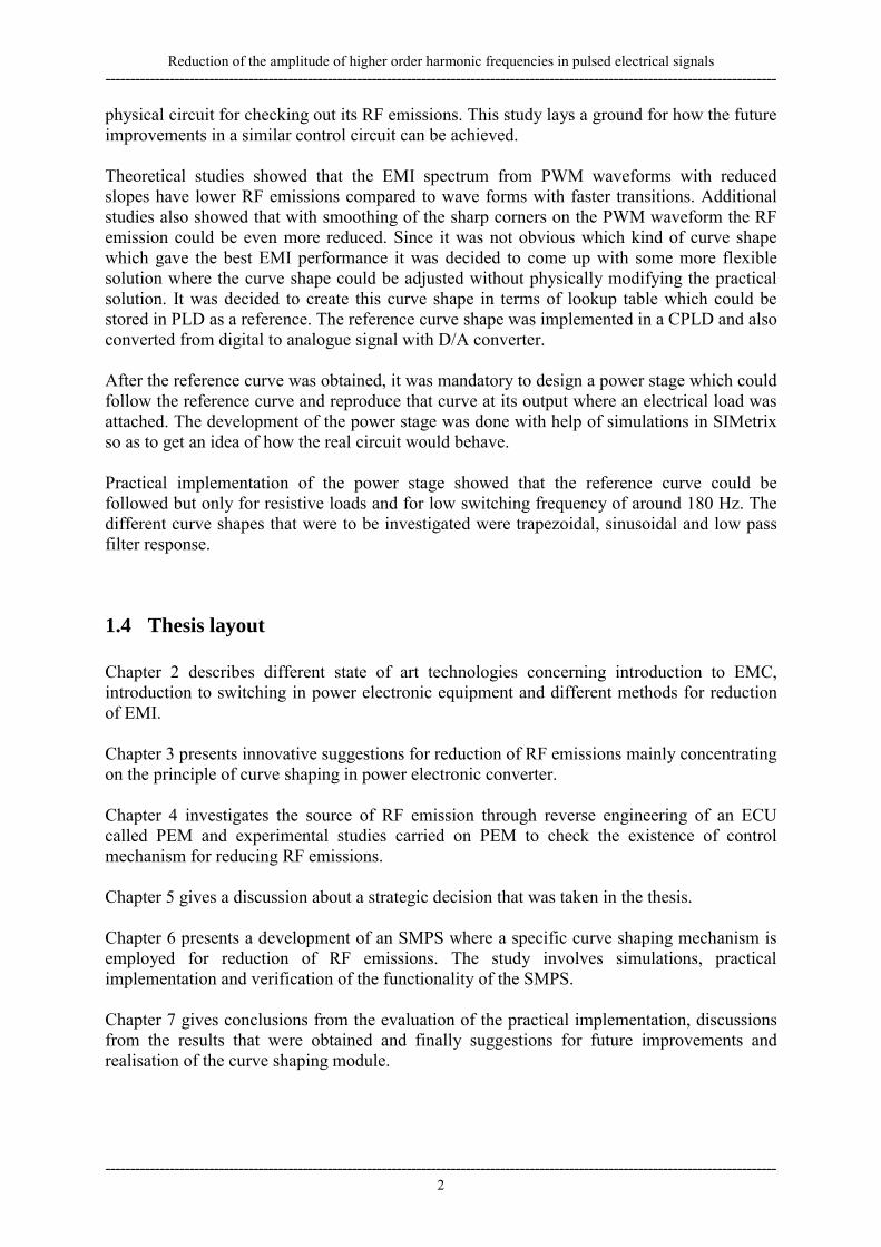
5.4 Measurements of conducted emissions _______________________________________ 69 5.4.1 Conducted emissions with the help of spectrum analyzer _____________________________ 69
5.4.1.1 Description of test setup with spectrum analyzer __________________________________ 69 5.4.1.2 Measurements using the current probe connected to spectrum analyzer ________________ 70
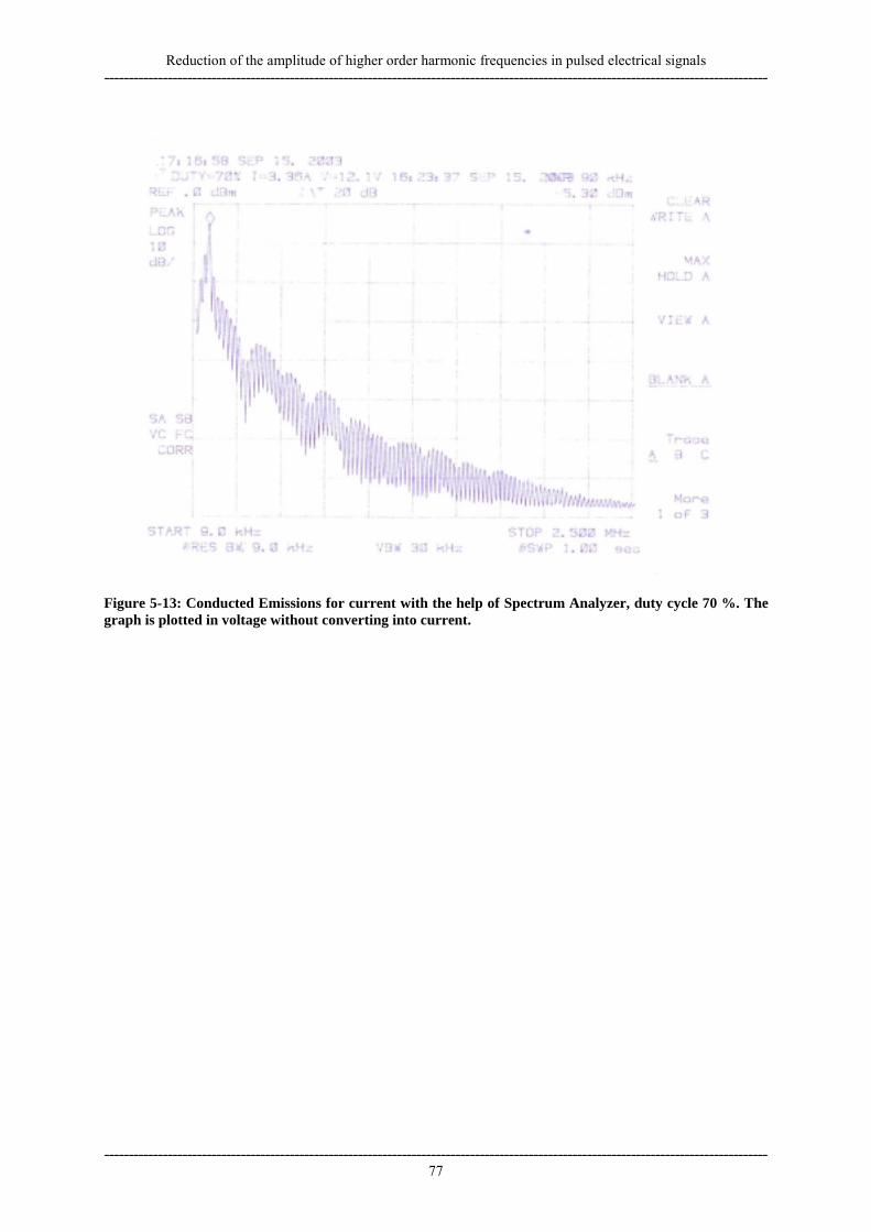
5.4.2 Description of test setup with oscilloscope_________________________________________ 78 5.4.2.1 Measurements on the output from PEM with help of oscilloscope _____________________ 79
5.5 Analysis of the graphs obtained from measurements ___________________________ 82 5.5.1 Analytical observations________________________________________________________ 82 5.5.2 Investigation of the effect of spikes on the frequency spectrum ________________________ 83
5.5.2.1 Waveform with positive spike _________________________________________________ 84 5.5.2.2 Waveform with positive and negative spike _______________________________________ 84
5.5.3 Investigation of ringing phenomenon ____________________________________________ 85 5.5.3.1 Variation of the ringing frequency fr ____________________________________________ 86 5.5.3.2 Variation of damping constant α _______________________________________________ 87
5.5.4 Aliasing Frequencies _________________________________________________________ 89 5.5.5 Application of the spectral density function _______________________________________ 90
6 Flexible curve shaping module _____________________________________________99 6.1 Investigation for implementation of Lookup table______________________________ 99 6.2 Micro-controller or PLC __________________________________________________ 99 6.3 What is CPLD? _________________________________________________________ 100
6.3.1 Programming of CPLD ______________________________________________________ 100 6.4 Choice of Module________________________________________________________ 102 6.5 Implementation of Lookup table ___________________________________________ 102
6.5.1 Simulation and verification of VHDL code _______________________________________ 103 6.6 Hardware implementation and measurement results __________________________ 104
6.6.1 CPLD – programming and measurements _______________________________________ 104 6.6.2 D/A – converter – Circuitry and measurements ___________________________________ 105
6.6.2.1 Measurements on D/A-output ________________________________________________ 107 6.7 Investigation for implementation of Power Stage _____________________________ 108
6.7.1 Amplifier-filter stage_________________________________________________________ 108 6.7.2 Selection of operational amplifier ______________________________________________ 110 6.7.3 Simulation of amplifier circuit _________________________________________________ 111 6.7.4 Amplifier circuit consisting of three operational amplifiers __________________________ 113
6.7.4.1 Simulation of three op-amp amplifier circuit_____________________________________ 114 6.7.4.2 Physical implementation of three op amp configuration____________________________ 115
ix
6.8 Power stage design ______________________________________________________ 116 6.8.1 Simulation of the Power Stage _________________________________________________ 118 6.8.2 Physical implementation of power stage _________________________________________ 119
6.8.2.1 Selection of components for power stage________________________________________ 120 6.8.2.2 Heat sink determination_____________________________________________________ 121 6.8.2.3 Positioning of components in Power Stage ______________________________________ 126
6.9 Testing of complete setup _________________________________________________ 127 6.9.1 Observation I – Driving stage__________________________________________________ 128 6.9.2 Modification I - Driving stage _________________________________________________ 128 6.9.3 Observation II – Feedback filter _______________________________________________ 128 6.9.4 Modification II - Feedback filter _______________________________________________ 128 6.9.5 Observation III – Human body capacitance ______________________________________ 128 6.9.6 Modification III - Human body capacitance ______________________________________ 128 6.9.7 Observation IV – Tuning of feedback gain _______________________________________ 129 6.9.8 Modification IV – Tuning of feedback gain ______________________________________ 129 6.9.9 Observation V – Additional DC-offset ___________________________________________ 130 6.9.10 Modification V – Additional DC-offset __________________________________________ 130
6.10 Employment of different lookup tables ____________________________________ 131 6.10.1 Output from power stage with trapezoidal reference________________________________ 131 6.10.2 Output from power stage with low pass filter reference _____________________________ 132 6.10.3 Employment of two different lookup tables _______________________________________ 133 6.10.4 Frequency response _________________________________________________________ 134 6.10.5 Limitations of the test setup ___________________________________________________ 135 6.10.6 Frequency spectrums from Dynamic Signal Analyser:______________________________ 136
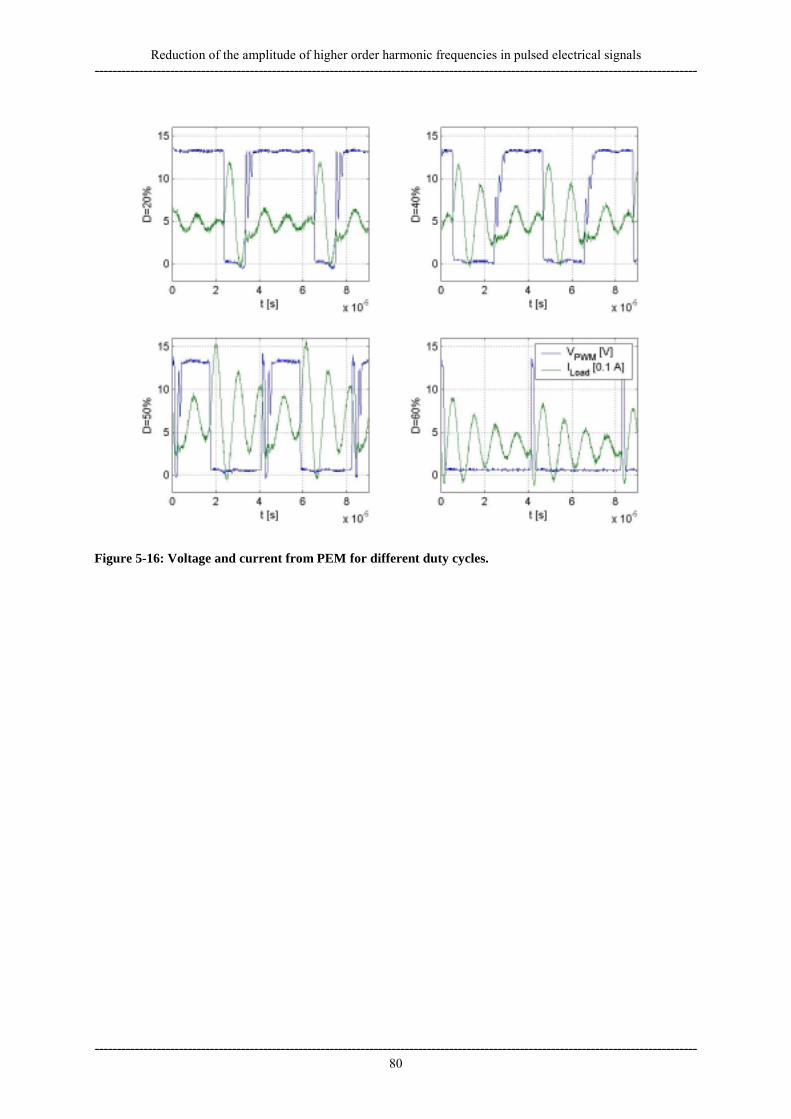
6.11 DC-motor load connected to the control circuit _____________________________ 138 6.12 Judgement of measurements on the power stage ____________________________ 139
Discussions and Conclusions ________________________________________________140 Limitations of the control circuit ________________________________________________ 140 Future implementation of power stage ___________________________________________ 141
Appendix: VHDL code for lookup table __________________________________________ I
x
xi
List of abbreviations AMN Artificial Mains Network ASIC Application Specific Integrated Circuit CMRR Common Mode Rejection Ratio CPLD Complex Programmable Logic Device ECU Electronic Control Unit ECM Electronic Control Module EMI Electromagnetic Interference EMC Electromagnetic Compatibility EUT Equipment Under Test FFT Fast Fourier Transform GPS Geostationay Positioning Satellite LISN Line Impedance Stabilization Network PEM Pump Electronic Module PLC Programmable Logic Circuit PWM Pulse Width Modulation RF Radio Frequency RPWM Randomized Pulse Width Modulation SCR Silicon Controlled Rectifier SMPS Switched Mode Power Supply TPM Tyre Pressure Monitoring VCO Voltage Controlled Oscillator VLSI Very Large Scale Integrated Circuit VSC Voltage Source Converter ZVS Zero Voltage Switching ZCS Zero Current Switching
xii
Reduction of the amplitude of higher order harmonic frequencies in pulsed electrical signals ----------------------------------------------------------------------------------------------------------------------------------------
1.1 Definition of the problem Since the beginning of 1970 a rapid evolution has taken place in automobiles in terms of introduction of more electronic equipment in cars. Many of these electronic equipment demands control of power for improved performance and functionality. This control of power is generally carried out with help of power electronic equipment. The power electronic equipment employs switching techniques of dc-to-dc conversion for limiting the power losses in the equipment. Switching of the power in electronic equipment causes RF emissions [4], which leads to interference with other electronic equipment. One of the problems in cars is that coupling between the radio receiver and a radiating source may lead to audible noise from the speaker system [18]. Various techniques have been suggested for reducing this RF emission generated by switching. The conventional methods for reducing RF emission are e.g. EMI filters [2] and shielding [2]. EMI filters are associated with the drawbacks that they generally occupy extra space, which can be hard to find in cars, and tuning of them requires lots of effort. The shielding method does not eliminate the RF emission from the source itself but instead it hides the RF emission so that it does not couple with other electronic equipment. This method also sometimes requires extra space and cooling of the equipment becomes trickier when the equipment is in built.
1.2 Aim of thesis The aim of the thesis is to investigate different strategies for lowering RF emissions from dc-to-dc PWM converters. The extent of the thesis and the result to be accomplished were independent of any specific goal requirements, rather the goal was to come up with some solution for lowering the RF emission from dc-to-dc PWM converter which could be implemented in practical circuit.
1.3 Summary of thesis Initialisation of the work was to get acquainted with fundamentals of EMC theory and investigating various techniques that have been analysed in principle. Studying these topics involved reading of EMC books and searching for IEEE papers. The aim of this study was to get some clue of which strategies were possible to realise in practice. Along with this study some own innovations were considered and simulated in MATLAB Simulink for checking their EMI performance. After achieving theoretical knowledge it was decided to carry out a study on a control circuit for fuel pump employed in Volvo Cars so as to get a physical idea for carrying out experimental work. This gave a picture for performing experimental investigations on a
Reduction of the amplitude of higher order harmonic frequencies in pulsed electrical signals ----------------------------------------------------------------------------------------------------------------------------------------
physical circuit for checking out its RF emissions. This study lays a ground for how the future improvements in a similar control circuit can be achieved. Theoretical studies showed that the EMI spectrum from PWM waveforms with reduced slopes have lower RF emissions compared to wave forms with faster transitions. Additional studies also showed that with smoothing of the sharp corners on the PWM waveform the RF emission could be even more reduced. Since it was not obvious which kind of curve shape which gave the best EMI performance it was decided to come up with some more flexible solution where the curve shape could be adjusted without physically modifying the practical solution. It was decided to create this curve shape in terms of lookup table which could be stored in PLD as a reference. The reference curve shape was implemented in a CPLD and also converted from digital to analogue signal with D/A converter. After the reference curve was obtained, it was mandatory to design a power stage which could follow the reference curve and reproduce that curve at its output where an electrical load was attached. The development of the power stage was done with help of simulations in SIMetrix so as to get an idea of how the real circuit would behave. Practical implementation of the power stage showed that the reference curve could be followed but only for resistive loads and for low switching frequency of around 180 Hz. The different curve shapes that were to be investigated were trapezoidal, sinusoidal and low pass filter response.
1.4 Thesis layout Chapter 2 describes different state of art technologies concerning introduction to EMC, introduction to switching in power electronic equipment and different methods for reduction of EMI. Chapter 3 presents innovative suggestions for reduction of RF emissions mainly concentrating on the principle of curve shaping in power electronic converter. Chapter 4 investigates the source of RF emission through reverse engineering of an ECU called PEM and experimental studies carried on PEM to check the existence of control mechanism for reducing RF emissions. Chapter 5 gives a discussion about a strategic decision that was taken in the thesis. Chapter 6 presents a development of an SMPS where a specific curve shaping mechanism is employed for reduction of RF emissions. The study involves simulations, practical implementation and verification of the functionality of the SMPS. Chapter 7 gives conclusions from the evaluation of the practical implementation, discussions from the results that were obtained and finally suggestions for future improvements and realisation of the curve shaping module.
Reduction of the amplitude of higher order harmonic frequencies in pulsed electrical signals ----------------------------------------------------------------------------------------------------------------------------------------
2 Theoretical studies This study gives an overview of aspects related to EMC issues concerning automobile industries. In the second half of the study, an investigation pertaining to functionality of converters as a part for generation of RF emissions in existing state of art technologies has been accomplished.
2.1 Introduction to EMC EMC means electromagnetic compatibility. It means that how much electromagnetic noise can be withstood by the receiver from the source generating electromagnetic noise. A device is electromagnetically compatible if it tolerates the electromagnetic environment and its effects are tolerated by all other devices operating in the same environment. EMC can be classified basically in two broad categories; one is called electromagnetic emissions and second is called electromagnetic susceptibility. Electromagnetic emissions can be divided again in two broad categories; one is called conducted emission and second is called radiated emission. With the rapid increase in power semiconductors and power electronics, interference levels on power mains have increased significantly in intensity and frequency of occurrence. Various techniques have been developed to study the EMI (Electromagnetic interference) problems and to find a unique solution to this problem. Any electrical equipment, especially semiconductor circuits can be qualified as a potential source of EMI. In general electrical apparatus can be classified in two principal categories. Equipment whose primary function is to generate and utilize the intentional high frequency signals and others are those that generate unintentional high frequency electromagnetic signals as a by-product of their primary functions. These signals basically appear as electromagnetic noise in the environment. The EMI is originating because of quick voltage and current transitions. Some of the important EMI sources can be given as follows: switches, electrical cleaning equipment, fluorescent tubes and power electronic equipment. Classification of these electromagnetic disturbances can be done on the basis of character frequency content and the transmission mode. The standard range of radio frequency disturbances starts at around 150 kHz. This range is divided in the bands of 0.15 to 30 MHz and from 30 to 1000 MHz. The standard limits and procedures for the measurement of radio disturbances are in the frequency range of 150 kHz to 1000 MHz. This standard is applicable to any electrical or electronic equipment intended to be used in vehicles. CISPR (Comité International Special des Perturbations Radio electriques or International Committee for the Radio Interference) [1] was the first international organization authorized to promulgate international recommendations on the subject of radio interference. EMI components in the range of 0.15 to 30 MHz are measured by EMI receivers. The EMI receivers measure the output voltage of suitable sensors. 2.1.1 Classification of Signals Noise signals are narrow band if the spectrum components are found at discrete frequencies with very narrow bandwidth. The frequency spectrum of a broadband disturbance is continuous. They are divided into two additional groups; the coherent and non coherent
Reduction of the amplitude of higher order harmonic frequencies in pulsed electrical signals ----------------------------------------------------------------------------------------------------------------------------------------
signals. A signal or emission is said to be coherent when neighbouring frequency increments are well defined in both amplitude and phase. For broad band situations, neighbouring amplitudes are approximately equal. For broadband emission the following conditions are also necessary [1]: While tuning the measuring bandwidth of the EMI instrument over the range of +2 or -2 dB around its centre frequency, a change in peak response is detected of 3 dB or less. Electromagnetic emissions produced by the power electronic equipment are always broadband and coherent in the range from the operating frequency to the number of few MHz. Electromagnetic disturbances can appear in the form of the common mode and differential mode components as shown in Figure 2-1.
I2 V2
Current I1
V1
Differential Mode Current =Id= (I1– I2)/2
C3
C1 C2 R1
Current I2
Common Mode Current =Ic= I1 + I2
Common Mode Voltage =Vc=(V1+V2)/2
Differential Mode Voltage =Vd= V1-V2
Id
Id
Ic /2
Ic/2
Vd
I1
Figure 2-1: Differential Mode and Common Mode EMI voltage and current components in a typical EMI source. They are divided as differential mode voltage component, differential mode current component, common mode voltage component and common mode current component. Various kind of detectors are required for the EMI measurement techniques including peak slide-back, average, effective (RMS), and quasi peak detectors [1]. 2.1.2 Introduction to EMC problems
Reduction of the amplitude of higher order harmonic frequencies in pulsed electrical signals ----------------------------------------------------------------------------------------------------------------------------------------
The basic concepts of electromagnetic interference are quite simple. The disturbance which may be an unwanted signal or electromagnetic noise can enter a victim receiver by the so called front door or back door. Entry by the front door refers to any undesired disturbance at a receiver input terminal used by the desired signal, whereas the back door refers to any other path such as being conducted into the primary power line inputs, induced interconnecting signal and control cables and radiated directly through equipment cases as shown in Figure 2-2.
Peripheral
Input
AC power out Front Door
Receiver
Back Door
Figure 2-2: Means of entry by radiated disturbances. Examples of the sources of EMI are as follows: 1. Properly operated transmitter at image frequency. 2. Improperly modulated transmitter. 3. Receiver local oscillator or super regenerative emission. Examples of the receivers are: 1. Inadequate front end selectivity. 2. Front end overload by a strong source. 3. Inter modulation and Cross modulation. 4. Inadequate power line filtering. 5. Inadequate case shielding Examples of the non receivers are as follows: 1. Computer system. 2. Telephone systems. 3. Security systems.
2.1.2.1 Coupling Paths [2] The most common means of the conductive coupling occurs at the antenna input terminals, electrical power inputs, control and interconnecting cables. Means of entry by conducted coupling is as shown in Figure 2-3.
Reduction of the amplitude of higher order harmonic frequencies in pulsed electrical signals ----------------------------------------------------------------------------------------------------------------------------------------
Figure 2-3: Means of entry by conducted disturbances. Antenna input terminals are designed to introduce the signals into receiver. Usually some broad selectivity characteristics are attached in an antenna. Despite these characteristics, a strong unwanted signal may not be sufficiently separated in frequency or far enough of the main beam of antenna to prevent interference unless the receiver itself is identically designed for that purpose or special mitigation techniques are employed.
2.1.2.1.1 Power line inputs [2] Receivers and other electronic equipment are often operated from commercial power introduced at the electrical input. These inputs are fed by the power lines to which sources of electrical noise may be attached and into which undesired signals may be coupled by induction or radiation. They are rejected by low pass power line filters.
2.1.2.1.2 Control and interconnecting cables [2] The lengthy cables may have electromagnetic disturbances induced in them and then conducted into equipment cases. Although such signals are conducted into equipment cases they constitute mainly inductive coupling.
2.1.2.1.3 Ground Returns [2] Ground returns are ideally equipotent surfaces. Even for such ideal ground planes, equipment cases are connected to them by wires of none zero impedance particularly at the higher frequencies .This finite impedance is common to both power output circuits and sensitive input circuits. Consequently grounding current flowing from the output circuits is converted into an input signal in sensitive input circuits. It is better to ground each circuit individually or when that is impractical to ground each circuit individually. Another method is to ground in equipment or system at many points to minimize coupling through ground returns and the ground plane itself. The two approaches are mainly single point grounding or multi point grounding.
Reduction of the amplitude of higher order harmonic frequencies in pulsed electrical signals ----------------------------------------------------------------------------------------------------------------------------------------
2.1.2.1.4 Inductive and Radiated Coupling [2] Radiated fields are those that escape completely from the source where as inductive coupling drop off completely with the distance. Inductive coupling is the one between cable and cable and it is minimized by the adequate spatial separation and by running cables at right angles to the each other or as nonparallel, as practical cables are also sources of radiation to other equipment. Internal to the equipment, inductive coupling between board traces is a common problem. Signals which are both desired and undesired may not necessarily arrive at the receiver by means of a direct path or may arrive by means of more than one path. In the case of an unwanted signal, the direction of arrival may have been changed from a null of a directional receiving antenna to its main lobe where it then appears at the receiver input terminals stronger than anticipated. Unintentional electromagnetic coupling between the conductors (wires and printed circuit boards) that are in close proximity is called a crosstalk. The mathematical model describing this coupling is called the multi conductor transmission model.
2.1.2.2 Differential and Common Mode Currents [2] The differential mode current and the common mode currents flow through the two phase conductors. The differential mode current is equal in magnitude but opposite in direction at a cross section on the line. This is the desired current that is assumed by the designers of the product. The common mode current is the undesired component of the current and is not necessary for the functional performance of the circuit. They are difficult to predict and their existence depends on the non ideal aspects of the structure such as asymmetries. Emissions from common mode currents are larger than the differential mode currents [2]. Figure 2-4 shows an example of differential mode and common mode currents in a three phase system.
Reduction of the amplitude of higher order harmonic frequencies in pulsed electrical signals ----------------------------------------------------------------------------------------------------------------------------------------
Figure 2-4: The contributions of differential-mode and common-mode currents to radiated emissions. I1 and I2 represent the currents in forward and the return path respectively for phase A.
2.1.2.2.1 Methods to reduce emissions from differential and common mode currents To reduce the emission levels due top the differential mode currents there are two options [2]:
1. Reduce the current level 2. Reduce the loop area
One can reduce the current level by reducing the peak levels of the functional signals. Also the current levels can be reduced by decreasing the pulse rate, rise time or fall time. The loop area can be reduced by using dedicated return signal conductor or using a gridded ground system or using multi layer boards as shown in Figure 2-5.
Reduction of the amplitude of higher order harmonic frequencies in pulsed electrical signals ----------------------------------------------------------------------------------------------------------------------------------------
Figure 2-5: Effects of loop area on radiated emissions from differential mode current. Reassigning them to keep the signal and its return adjacent to each other reduces the loop area and hence the emissions of the differential mode current by a factor of 3 dB or 10 dB. In order to reduce the emission levels of the common mode currents it is necessary to:
1. Reduce the levels of the common mode current. 2. Reduce the length of the conductors.
A current probe can be used to measure the noise currents that pass out of the power chord. To measure the conducted emissions LISN (Line Impedance Stabilization Network) is used. Commercial power passes unimpeded through, but the noise currents generated in the product are sampled in the LISN and measured by the spectrum analyzer or tuned receiver. The first set is the differential mode currents which pass out the phase conductor and return on the normal conductor. The second set is the common mode currents which pass out the phase and neutral conductors and return on to the green wire as shown in Figure 2-6.
Reduction of the amplitude of higher order harmonic frequencies in pulsed electrical signals ----------------------------------------------------------------------------------------------------------------------------------------
Figure 2-6: Use of LISN to measure conducted emissions for A.C mains
Utilization of LISN There are two primary goals of using LISN:
1. To present constant impedance to the products power input over the frequencies of the conducted emissions regulatory limit.
2. To block or prevent the noise signals on the commercial power grid from contaminating the measurement.
The first condition is required because the input impedance looking into the power distribution between the phase and the green wire and between the neutral and green wire vary considerably with the frequency and vary from installation to installation. As shown in Figure 2-7 the capacitors C1 = C2 = 1 µF shunt the noise coming from the power grid. Similarly the two inductances, L1 and L2, block the remaining noise coming from the power grid. These two components give the LISN the ability to satisfy the second criterion. Noise signals on the commercial power net do not contaminate the measurement. The first criterion is attained by the placement of the two resistors R2 and R4. R2 represents the input impedance to the measurement device and R4 is a dummy load. The capacitor C3 prevents any direct current from overloading the measurement device and the resistors R1 and R3 are present to discharge those capacitors in the event that R2 or R4 resistors are disconnected. Thus over the regulatory limit frequency range over the product essentially sees 50 Ω between the phase and green wire and between neutral and green wire.
Reduction of the amplitude of higher order harmonic frequencies in pulsed electrical signals ----------------------------------------------------------------------------------------------------------------------------------------
2.1.2.3 EMI in power electronic equipment [1] Power semiconductors produce high frequency noise as operational by-product. The repetition rate of these high frequency disturbances is more compared to normal electromechanical switches like relays. Therefore it becomes necessary to study the effect of high frequency disturbances in power electronic equipment or power semiconductors separately.
2.1.2.3.1 EMI from rectifiers [1] A rectifier acts as short circuit for forward bias and open circuit for reverse bias [1]. The switch on and off operation of the rectifier is shown in Figure 2-8.
Reduction of the amplitude of higher order harmonic frequencies in pulsed electrical signals ----------------------------------------------------------------------------------------------------------------------------------------
Figure 2-8: Rectifier switch in on and off operation. The on state current increases quickly and a high on state voltage appears across the rectifier. The voltage falls back to its normal value in the time interval tf. This time is needed for charge carriers to get into the depletion region. The voltage spike is actually a broad band emission. The rectifier produces a much higher emission during its switch off operation. On-state current decreases to zero during time interval t0. The current turns to negative due to stored charge in form of minority carrier in the depletion region. The amount of stored charge carrier is characterized by the diffusion capacity. As the reverse current IMaxReverse can be quite large, high voltage transients appear with the wide frequency spectra in the inductance of conductors and connecting circuits. The interference effect can be reduced partly by limiting the magnitude of the surge current and partly by decreasing the slew rate of the negative surge current.
2.1.2.3.2 EMI from SCRs [1] HF noise levels are much higher at switch on than at switch off. The depletion region looses its insulating capacity after a given time called the delay time. The quick collapse of the anode cathode voltage generates high frequency disturbances and the switching time is about 0.5 to 2 µs, so the spectra of the generated HF noise can be quite wide. The switch on characteristics of SCRs can be obtained from Figure 2-9.
Reduction of the amplitude of higher order harmonic frequencies in pulsed electrical signals ----------------------------------------------------------------------------------------------------------------------------------------
2.1.2.3.3 EMI from power transistors [1] The switching time for power transistors is much shorter than for the SCR. The collector current continues to flow until the time ts until the time called the storage time. During this time interval charge carriers would be removed from the depletion region. After the storage time the collector current falls to zero. The fall time of the collector current is rather short usually in the range of approximately 10 ns to 100 µs depending on the rated power of the transistor. Therefore the EMI produced by the power transistor is much wider than that produced by the SCR, refer to Figure 2-10.
t t
t t td
IB IB
IC
ton ts toff
Vce IC Vce
Switch On Switch Off
t0 t0
Figure 2-10: Power transistor switch processes.
2.1.2.3.4 EMI from controlled rectifier circuits [1]
Reduction of the amplitude of higher order harmonic frequencies in pulsed electrical signals ----------------------------------------------------------------------------------------------------------------------------------------
It is very necessary to gather preliminary data for solving EMI problems in controlled rectifier circuits. For this EMI generated from these controlled rectifier circuits is measured as a function of load rating, load character and the firing angle.
EMI as a function of the output power [1] Figure 2-11 describes the various conditions for various load and firing angles [1]:
1. Curve 1 - without delay angle and with nominal load. 2. Curve 2 - without delay angle but one fifth of the nominal load. 3. Curve 3 - with a 70 degree firing angle nominal load. 4. Curve 4 - with 70 degree firing angle and one third of load.
EMI seems to be nearly independent of the load current. The explanation is that the switch-on process of the SCR, being a voltage ramp is principally independent of the load current. The interference is generated only by SCR switch off, which depends on the load current. This can be seen from Figure 2-11.
dBµV
Curve 3
Curve 4
Curve 1Curve 2
MHz
Figure 2-11: EMI from SCR control with different output powers and firing angle. The curves are just approximated, but show the tendency that is reflected in a real measurement.
EMI as a function of the character of the load [1] Figure 2-12 shows an approximated tendency of EMI performance for different loading conditions. The different curves are describes as follows:
Reduction of the amplitude of higher order harmonic frequencies in pulsed electrical signals ----------------------------------------------------------------------------------------------------------------------------------------
1. Curves 1 and 2 – Representation of the tendency for a chopper circuit for resistive
load and resistive-inductive load respectively. 2. Curve 3 - Shows the EMI of the rectifier circuit with a resistive load. 3. Curve 4 - Shows the same with the resistive-inductive load.
Curve 1
Curve 2Curve 4
Curve 3
dBµv
MHz
Figure 2-12: EMI of SCR control at different load type. As can be seen the emissions of the SCR control did not depend on the character of the load, except for the case with the resistive-inductive load where the emissions are slightly higher.
EMI from the semiconductor equipment EMI generated by power electronic is often that of a pulse train, since rectification involves repetitive switching from conduction to cut off. The repetition rate is some multiple of the operating frequency depending on the circuit configuration.
2.1.2.4 Broken line envelope analysis EMI evaluation can be carried out with the help of the broken line envelope and instead of performing the discrete harmonic analysis of the waveform, it is better to define the spectrum of the single impulse in the pulse train. Referring to Figure 2-13, the spacing of the spectral lines is determined by the repetition rate of the pulse train. Therefore, as the repetition rate decreases, the spectral lines come close together with the sinx/x function and its 1/x envelope is coming close together as the width of the impulse increases. Finally a step impulse would have the envelope completely filled with spectral lines as visible from Figure 2-13.
Reduction of the amplitude of higher order harmonic frequencies in pulsed electrical signals ----------------------------------------------------------------------------------------------------------------------------------------
2.1.2.4.1 Example for plotting the EMI spectrum Let us plot the spectrum of a trapezoidal impulse series with the following characteristics:
1. Amplitude A = 50 V. 2. Time duration of single pulse τ = 5 µs. 3. Rise and fall time; tr = tf =0.05µs.
We can study the emission from the range of 10 kHz to 30 MHz. The value for selecting the horizontal section is A(τ+t) = 250 µs corresponding to the 168 dBµV/MHz (8 dB above the 168 dB mark) and goes to the line of the A = 50 V. The intersection of the second section is about 70 kHz. Above this frequency spectrum the spectrum continues with the –20 dB/decade slope down to the crossing at A/t = 1000 line i.e. to about 7 MHz. Above this frequency the spectrum is formed by a straight line of -40dB/decade slope. This spectrum is shown in Figure 2-14.
Reduction of the amplitude of higher order harmonic frequencies in pulsed electrical signals ----------------------------------------------------------------------------------------------------------------------------------------
Figure 2-14: Spectrum of a trapezoidal impulse with 50 V amplitude, 5 µs duration and 0.05 µs rise time. 2.1.3 EMC in Automobiles (CISPR standards for the measurements of radio disturbances
for the protection of receivers used in the vehicles) This standard refers to the limits and procedures for the measurement of the radio disturbances in the frequency range of 150 kHz to 1000 MHz. It applies to any electronic/electrical equipment intended for use in vehicles and large devices. These limits are meant for the protection of the receivers installed in the vehicle from disturbances produced by the component/modules in the same vehicle. The receiver types to be protected are sound and television receivers, land mobile radio, telephone, GPS, remote opening, TPM, Blue tooth and amateur citizen's radio. Vehicles are limited to the passenger cars, truck, agricultural tractors and snow mobiles. CISPR standard does not include the protection of electronic control systems from radio frequency emissions, or from transient or pulse type voltage fluctuations. These subjects are expected to be included in the ISO publications. Mounting location also affects the vehicle body construction and harness design. For vehicular purpose tests at 150 kHz are considered to be adequate. For the purpose of this standard test frequency ranges have been generalized to cover the radio services in various parts of the world. Currently valid international standards used at present are as follows. 1. International Electro technical Vocabulary – IEC 50(161). 2. CISPR 12:1990 –Limits and methods of measurements of radio interference
characteristics of vehicles, motor boats, and spark ignited engine driven devices. 3. CISPR 16-1: 1993: Specification for radio disturbances and immunity measuring
apparatus and methods. Definitions:
Reduction of the amplitude of higher order harmonic frequencies in pulsed electrical signals ----------------------------------------------------------------------------------------------------------------------------------------
1. Receiver Terminal Voltage: The voltage generated by the source of radio disturbance and measured in dBµV by a radio disturbance measuring instrument conforming to the requirements of CISPR-1.
2. Component Continuous Conducted Emissions: The noise voltages/currents of a steady state nature existing on the supply or other leads of a component/module which may cause disturbance to reception in an on board receiver.
3. Antenna Matching Unit: A unit for matching the impedance of an antenna to that of the 50 Ω measuring receiver over the antenna measuring frequency range.
4. Antenna Correction Factor: The factor which is applied to the voltage measured at the input connector of the measuring instrument to give the field strength at the antenna. The antenna correction factor is comprised of an antenna factor and a cable factor.
5. Compression Point: The input signal level at which the gain of the measuring system becomes nonlinear such that the indicated output deviates from an ideal linear receiving system's output by the specified increment in dB.
6. Class: A performance level agreed upon by purchaser and the supplier and documented in the test plain.
7. Device: A machine which is not self propelled. The below mentioned definitions are necessary for the understanding of this standard and are contained in the IEC: 1. Artificial Mains Network: A network inserted in the supply mains lead of apparatus to be
tested which provides, in a given frequency range, specific load impedance for the measurement of disturbance voltages and which may isolate the apparatus from the supply mains in that frequency range.
2. Bandwidth: The width of the frequency band outside which the level of any spectral component does not exceed a specified percentage of a reference level.
3. Broadband Emission: An emission which has bandwidth greater than that of a particular measuring apparatus or receiver.
4. Disturbance Suppression: Action which reduces or eliminates the electromagnetic disturbance.
5. Disturbance Voltage or Interference Voltage: Voltage produced between the two points on two separate conductors by an electromagnetic disturbance measured under specific conditions.
6. Narrowband Emission: An emission which has bandwidth less than the particular measuring apparatus of the receiver.
7. Peak Detector: A detector, the output voltage of which is the peak value of an applied voltage signal.
8. Quasi Peak Detector: A detector having the specified electrical time constants which when regularly repeated identical pulses are applied to it, delivers an output voltage which is a fraction of the peak value of the pulses, the fraction increasing towards the unity as the pulse repetition rate is increased
9. Electromagnetic Environment: The totality of the electromagnetic phenomena existing at a given location.
10. Shielded Enclosures: A mesh or sheet metallic housing designed expressly for the purpose of separating electromagnetically the internal and the external environment.
For testing of vehicle for EMC test plan should be included. It should include the following things:
Reduction of the amplitude of higher order harmonic frequencies in pulsed electrical signals ----------------------------------------------------------------------------------------------------------------------------------------
1. Frequency range to be tested. 2. The emission limit. 3. The disturbance classification. 4. Antenna types. 5. Test report requirements. 6. Supply Voltages.
2.1.3.1 Categories of the Disturbance Sources Electromagnetic disturbances can be divided into three types: 1. Continuous/long duration broadband and automatically actuated short duration equipment. 2. Manually actuated short duration broadband. 3. Narrow band. Broad band disturbances in vehicles are ignition system, active ride control, fuel injection, wiper monitor, power antenna etc. Narrow band disturbances in vehicles are found in microprocessors, digital logic, oscillators, or clock generators.
2.1.3.2 Measuring Equipment Requirements [3] The measuring equipment noise floor shall be at least 6 dB less than the limit specified in the test plan.
2.1.3.2.1 Shielded Enclosure The ambient noise level should be at least 6 dB below the limits specified in the test plan for each test to be performed. The shielding effectiveness of the shielded enclosure should be sufficient to assure that the required ambient electromagnetic noise requirement level is met. The shielded enclosure should be of sufficient size so as to ensure that neither the vehicle nor the test antenna should be closer than the 2 m from the walls or ceiling and 1 m to the nearest surface of the absorber material used.
2.1.3.2.2 Absorber Line Shielded Enclosure For radiated emission measurements, however, the reflected energy can cause errors of as much as 20 dB. Therefore it is necessary to apply RF absorber material to the walls and ceiling of a shielded enclosure that is to be used for radiated emissions measurements. No absorber material is required for the floor.
2.1.3.2.3 Receivers
Reduction of the amplitude of higher order harmonic frequencies in pulsed electrical signals ----------------------------------------------------------------------------------------------------------------------------------------
Scanning receiver which meets the requirement of CISPR is satisfactory for measurements. Either manual or automatic frequency scanning may be used. Special consideration shall be given to the overload, linearity, selectivity, and the normal response to pulses. While using quasi peak limits and a peak detector being used for time efficiency, any peak measurements at or above the quasi peak limit shall be re-measured using the quasi peak detector.
2.1.3.2.4 Broadcast Bands There are three types of broadcast bands: 1. Long Wave (150-300 kHz) 2. Medium Wave (0.53 to 2.0 MHz) 3. Short Wave (5.9 to 6.2 MHz) The measuring systems should have the following characteristics: 1. Output impedance of the impedance matching equipment: 50 ohm resistive. 2. Gain: The gain of the measuring equipment shall be known with an accuracy of ±0.5 dB.
The gain of the equipment shall remain within a 6 dB envelope for each frequency band. See gain curve in Figure 2-15.
6dBenvelope
fhighflow
Gain[dB]
Figure 2-15: Example of gain curve. 3. Compression Point: The 1 dB compression point shall occur at a sine wave voltage level
greater than 60 dB (TV). 4. Measurement System Noise Floor: The noise floor of the combined equipment including
measuring equipment, matching amplifier and a preamplifier shall be at least 6dB lower than the limit level.
5. Dynamic Range: From the noise floor to the 1 dB compression point. 6. Input Impedance: The impedance of the measuring system at the input of the matching
network must be at least 10 times the open circuit impedance of the artificial antenna network.
FM broadcast - 87 MHz to 108 MHz
Reduction of the amplitude of higher order harmonic frequencies in pulsed electrical signals ----------------------------------------------------------------------------------------------------------------------------------------
Measurements shall be taken with a measuring instrument which has an input impedance of 50Ω. If the standing wave ratio (SWR) is greater than 2:1, input matching network shall be used.
Communication bands - 30 MHz to 108 MHz The test procedure assumes a 50 Ω measuring instrument and a 50 Ω antenna in the frequency range of 30 MHz to 1000 MHz.
2.1.3.2.5 Test equipment unique to component module test [3] Below a list of the different requirements for the devices involved in the test equipment for a component module test is presented: 1. Power supply: EUT power supply shall have adequate regulation to maintain the supply
voltage within limits specified; +13.5 V to –0.5 V for 12 V systems and +27 V to –0.1 V for 24 V systems, unless otherwise specified in the test plan. The power supply shall be adequate filtered such that the RF noise produced by the power supply is at least 6dB lower than the limits specified in the test plan.
2. Battery: When specified in the test plan, a vehicle battery shall be connected in parallel with the supply.
3. Ground Plane: The ground plane should be made of 0.5 mm thick copper, brass or galvanized for the measurement of conducted or radiated emissions. The ground plane shall be bonded to the shielded enclosure such that the o.k. resistance shall not exceed 2.5 mΩ. In addition, the bond straps shall be placed at the distance number greater than 0.9 m apart.
2.1.3.2.6 Test equipment unique to the conducted emission measurements [3] There are two main devices associated with the test equipment for conducted emission measurements: 1. Artificial Mains Network (AMN): The AMN shall have nominal 5 µH inductance and
shall meet the impedance characteristics with a tolerance of ±10 %. The measuring port of all AMN shall be terminated with 50Ω load. For the purpose of this standard, AMN shall be used unto 108 MHz.
2. Current Probe: The current probe shall be selected considering the following; the size of the harness to be measured, the frequency range required by the test plan, and the sensitivity of probe necessary to measure the signals at the limit level.
2.1.3.2.7 Equipment unique to the measurements of component/module radiated emissions [3]
Reduction of the amplitude of higher order harmonic frequencies in pulsed electrical signals ----------------------------------------------------------------------------------------------------------------------------------------
The antenna correction factor is applied, and the antenna provides a 50 Ω match to the measuring receiver. For the purpose of this standard, the limits for antenna are fixed as follows: 1. 15 to 30 MHz - 1 m vertical monopole. 2. 30 to 200 MHz - a bi-conical antenna used in vertical and horizontal polarization. 3. 200 to 1000 MHz - a log–periodic antenna used in horizontal and vertical polarization.
Antenna Matching Unit [3] Correct impedance matching between the antenna and the measuring receiver of 50 Ω shall be maintained at all frequencies.
2.1.3.3 Measurement of Vehicle Component and Modules [3] This method applies to the suppression of the onboard radio disturbances for motor vehicles which is the main crux of the thesis. It also deals with the suppression of the devices and working machinery to achieve the acceptable radio reception within on-board radio receivers. The requirements contained the maximum permissible voltage, current and field strengths in the frequency range of 150 kHz to 1000 MHz.
2.1.3.3.1 Conducted Emissions from component/module Voltage measurements on all power leads shall be made relative to the case of the EUT (when the case provides the ground return path) or the ground lead as close to EUT as practical. For the EUT with return line remotely grounded, the voltage measurements should be made on each lead relative to the ground plane. The test harness shall be spaced by 50 mm above the ground plane.
2.1.3.3.2 Current Probe Measurements Current probe measurements shall be made on the control/signal leads as a single cable or in sub-groups as is compatible with the physical size of the current probe. The test harness length should be normally 1.5 m, spaced 50 mm above the ground plane. The test harness wires ideally should be parallel and adjacent unless otherwise specified. To assure that the maximum level is measured at the frequencies above 30 MHz, position the current probe in the following additional positions: 1. 500 mm from the EUT connector. 2. 1000 mm from the EUR connector. 3. 50 mm from the AN terminal.
Reduction of the amplitude of higher order harmonic frequencies in pulsed electrical signals ----------------------------------------------------------------------------------------------------------------------------------------
In most of the cases, the position of the maximum emission will be as close to the EUT connector as possible. Where the EUT is equipped with a metal shell connector, the probe shall be clamped to the cable immediately adjacent to the connector shell, but not around the connector itself. The EUT and all parts of the test set-up shall be a minimum of 100 mm from the edge of the ground plane.
2.1.3.3.3 Equipment Arrangement For voltage measurements the arrangement of the EUT and measuring equipment shall be as shown in the Figure 2-16 depending on the conducted emission test depending on the intended EUT installation in the vehicles: 1. EUT remotely grounded (power return line longer than 200 mm) 2. EUT locally grounded (power return line 200 mm or shorter)
2.1.3.3.4 Limits for Conducted disturbances of the components For acceptable radio reception in a vehicle, the conducted noise shall not exceed the specific values for broadband and narrow band limits respectively [3].
2.1.3.3.5 Limits for the Control Signals The limits for the radio frequency currents on the control signal lines are given in the form of predefined tables as shown in predefined tables in [3].
2.1.3.3.6 Radiated emissions from the component/module Conducted Emissions will contribute to the radiated emissions measurements because of radiation from the wiring in the test set-up. Therefore it is advisable to establish conformance with the conducted emissions requirements before performing the radiated emissions test. Measurements of Radiated field strengths must be made in ALSE to eliminate the high levels of extraneous disturbance from electrical equipment and broadcasting stations. Disturbance to the vehicle on-board receiver can be caused by direct radiation from more than one lead in the vehicle wiring harness. This coupling made to the vehicle receiver affects both the type of testing and the means of reducing the disturbance at the source. Vehicle components which are not effectively grounded to the vehicle by short ground leads or which have several harness leads carrying the disturbance voltage will require a radiated emissions test. This has been shown to give better correlation with the complete vehicle test for the components installed in this way.
Reduction of the amplitude of higher order harmonic frequencies in pulsed electrical signals ----------------------------------------------------------------------------------------------------------------------------------------
Test procedure for measuring radiated emissions from a component module The general arrangement of the disturbance source and connecting harness etc represents a standardized test condition. Any deviations from the standard test harness length shall be agreed upon to prior to the testing and recorded in the test object. The harness (power and control signal lines) shall be supported 50 mm above the ground plane by non conductive material, and arranged in a straight line. The EUT shall be made to operate under typical loading and other conditions as in the vehicle such that the maximum emission state occurs. These operating conditions must be clearly defined in the test plan to ensure supplier and customer are performing identical tests depending on the intended EUR installation in the vehicle. For test on an EUT with power return line remotely grounded, two artificial networks are required; one for the positive supply and one for the power return line. For test on an EUT with power return line locally grounded; one artificial network required for the positive supply line. EUT shall be wired as in the vehicle. The measuring port should be terminated with the 50 Ω load as shown in Figure 2-16.
Test harness 200 mm Power +
Supply -
Ground Plane
Aritificial Mains
Network
EUT
Insulating Spacer (50 m)
Aritificial Mains Network
Artificial Mains Network
Measuring Instrument
EUT
Elevation of the complete test set up
Coaxial Cable
Ground Plane
Plan of the complete test set up
Power - Supply +
Figure 2-16: Conducted emission test on an EUT with power return line remotely grounded.
Reduction of the amplitude of higher order harmonic frequencies in pulsed electrical signals ----------------------------------------------------------------------------------------------------------------------------------------
The face of the disturbance source causing the greatest radio frequency emission shall be closest to the antenna. Where this face changes with frequency, measurements shall be made in three orthogonal planes and the highest level at each frequency shall be noted in the test report. At frequencies above 30 MHz the antenna shall be oriented in horizontal and vertical polarization to receive maximum indication of the radio frequency noise level at the measuring receiver the distance between the wiring harness and the antenna shall be 1000+10 mm. This distance is measured from the centre of the wiring harness to: 1. the vertical monopole element. 2. the midpoint of the bucolical antenna. 3. the nearest part of the log periodic antenna. The EUT shall be mounted 100±10 mm from the edge of the test bench. This overall report describes a very general approach towards EMC. All the measurement techniques and results might not be useful for the reader. Especially only specific results and tables were used for the measurements for the studies carried out in the thesis work. Thus this introduction to EMC should be viewed as a general guideline to build an approach towards EMC, especially for those readers who are coming across EMC for the first time.
Reduction of the amplitude of higher order harmonic frequencies in pulsed electrical signals ----------------------------------------------------------------------------------------------------------------------------------------
2.2 Switching Theory 2.2.1 Introduction to Switching - DC-DC converters Generally, power electronic equipment are used where process and control of the flow of electric energy is required by supplying voltages and currents in a form that is suited for specific kind of loads. Most important considerations in power conversion processes are reduced power loss and achieving higher efficiency. This is required for removing the wasted energy and difficulty in removing heat generated due to dissipated energy. For example, this kind of conversion can be obtained by linear mode power supply or switched mode power supply. Both of them are used for dc input voltage and provide a fixed output dc voltage. Transistors are used in linear dc power supply so as to control the voltage between input voltage VD and output voltage VO. In linear mode power supply transistor is controlled to absorb the difference between input voltage and output voltage so as to obtain voltage regulation. As transistor is operating in linear region, it generally behaves like a resistor providing higher losses and thus resulting in lower efficiency. By operating transistor as a switch in high frequency i.e. either it is fully on or either it is fully off at a particular value of frequency of switching, e.g. 250 kHz, the dc voltage is converted into some biased ac voltage which is filtererd in order to obtain a new dc voltage level. This is the basic principle of SMPS or switched mode power supply as shown in Figure 2-17.
VO
VD
Vref
C
L
Load
Controller
Figure 2-17: Model of switched mode DC power supply, consisting of a step down DC-DC converter.
The transistor diode combination can be used as hypothetical switch like a two way switch as shown in Figure 2-18 . During turn on the switch is in position A, and during turn off the switch is in position B. As a result voltage across the switch, VD, equals the input voltage V during ton. During toff, the voltage across switch is equal to zero. Also there is addition of some ripple because of switching involved and some sort of L-C filter can be used to reduce this ripple and pass the average of input voltage so that output voltage is equal to the voltage
Reduction of the amplitude of higher order harmonic frequencies in pulsed electrical signals ----------------------------------------------------------------------------------------------------------------------------------------
across switch i.e. VO = VD, where VD is the input voltage across diode. VO is the average output voltage.
-
+V
A
B C
L
LoadVD
Figure 2-18: Equivalent Circuit for basic switch mode power supply.
Figure 2-19 shows the in principle how VO is obtained for a certain duty cycle.
VO
t
toff
TS
ton
VD V
Figure 2-19: Switching waveform in Switched Mode Power Supply.
From the waveform Figure 2-19 it can be derived that: Equation 2-1
DDS
on
T
OD
S
DVVTtdtV
TV
S
=== ∫1
0
From this equation as the input voltage changes, it is possible to regulate the output voltage VO by controlling the ratio of ton/TS, which is called the duty ratio D, of the transistor switch. Usually TS is kept constant and ton is adjusted. This is the basic concept of PWM. The transistor is operating as a switch which is either fully on or fully off, so it can be used to minimize power losses. If a higher switching frequency is selected, the harmonic content in the waveform can be easily reduced by means of small filter to yield the desired dc voltage. Selection of switching frequency depends also on the power dissipation in transistor which increases with the switching frequency. Thus higher switching frequencies can be used to synthesize output waveforms. Switching techniques can be classified in two types of switching:
Reduction of the amplitude of higher order harmonic frequencies in pulsed electrical signals ----------------------------------------------------------------------------------------------------------------------------------------
1. Hard switching techniques. 2. Soft switching techniques. 2.2.2 Hard switching technique using PWM control in DC-DC converters In any dc-dc converter, the average dc output voltage must be controlled with the help of a switch to control on and off duration. Pulse Width Modulated control means to keep the switching frequency constant and adjust the on duration of switch (transistor) to control the voltage. Variation in switching frequency might not be good solution because it makes it more difficult to filter the ripple components in the input and output waveforms of the converter. The controller, where the PWM pattern is generated, is shown in Figure 2-20.
Switched Signal to transistor, PWM VLoad -
Vref +
VRep -
VControl +
Comparator
Σ
Figure 2-20: Block Diagram of Pulse Width Modulator. The control signal is generated by comparing a control voltage with repetitive waveform as shown in Figure 2-21.
Vsupply
toff t
Vcontrol
t
VRep
PWM signal
ton
TS
Figure 2-21: Generation of PWM pattern for a dc-dc converter.
Reduction of the amplitude of higher order harmonic frequencies in pulsed electrical signals ----------------------------------------------------------------------------------------------------------------------------------------
The control signal Vcontrol is obtained by amplifying an error or the difference between actual output voltage VLoad and desired value Vref. The frequency of repetitive waveform is called switching frequency. When the amplified error signal, which varies slowly with time relative to switching frequency, is greater than the saw-tooth waveform, switch control signal becomes high causing the switch to turn on or else the switch remains off. Total duty ratio D can be expressed as [4]: Equation 2-2
D
O
S
on
VV
meofwaveforpeakvoltagtagecontrolvol
Tt
D ===
As seen from Equation 2-2 above, by varying the ratio ton/TS of switch, output voltage VO can be controlled. Switches in practice can be transistors like BJT, MOSFET and HEXFET etc.
When the load is of inductive character, additional energy stored in inductance has to be released. The switch will have to absorb this inductive energy and might get destroyed during turnoff process. By using a diode in parallel with the load, inductive energy can be dissipated through this diode. Voltage fluctuations can be diminished largely by providing a low pass filter consisting of an inductor and capacitor.
2.2.2.1 Principle of Working of step down DC-DC Converter As shown in Figure 2-22 during the switch on period, the diode becomes reverse biased and input provides energy to load as well as to the inductor. During the switch off period, the inductor current flows through the diode which provides energy to the load. The average current through the inductor will be equal to the average output current. For normal operating conditions, here it is assumed that current flowing through the inductor is continuous.
+ VO
-
+ VO
-
+ VL -
+ VL -
Switch off
Switch on
-
+ V C
L
Load
VD
-
+ V C
L
Load
VD
Figure 2-22: Equivalent circuit for the step down dc-dc converter in on and off operation.
Reduction of the amplitude of higher order harmonic frequencies in pulsed electrical signals ----------------------------------------------------------------------------------------------------------------------------------------
During on period the voltage across the inductor can be expressed as: Equation 2-3
OL VVV −= This causes a linear increase in the inductor current and when the switch is turned off, because of inductive energy storage, current continues to flow through the load and voltage across inductor is: Equation 2-4
OL VV −= The integral of inductor voltage over one switching period TS should be zero:
Equation 2-5
00 0
=+= ∫∫ ∫ dtVdtVdtVS
on
S on T
tL
T t
LL
The area occupied is divided in two sub areas A and B as shown in Figure 2-23 which are equal: Equation 2-6
DTt
VV
tTVtVVS
onOonSOonO ==⇒−=− )()(
Reduction of the amplitude of higher order harmonic frequencies in pulsed electrical signals ----------------------------------------------------------------------------------------------------------------------------------------
Figure 2-23: Behaviour of current through inductor during turn on and turn off in step down DC-DC converter.
The instantaneous input current jumps from peak value to zero every time the switch is turned off. Thus for a step down converter, the output voltage depends purely on the duty cycle and not any other circuit parameter. It is assumed that the current has continuous mode of conduction rather than discontinuous mode of conduction as variation.
2.2.2.2 Limitations of Hard Switching Although devices like IGBT, MOSFETS used for switching are moving towards ideal switching behaviour nowadays with good MOS input gate, high switching speed, low conduction voltage drop, very high current carrying capability and also higher degree of robustness, there are certain limitation in hard switching using PWM control. Although switching speed has increased nowadays, switching losses are introduced during turn on and turn off process of devices like IGBT, MOSFETS. This leads to excessive voltage and current transients in the device used for switching. Losses are also introduced although the switching is fast because of parasitic inductance among the components and interconnections in the circuit. There is also large amount of stored charge in the devices like MOSFET or other switching devices which increases losses. Another issue is the transient on the device output voltage caused by device switching, resulting in dv/dt's in excess of 5-10 volts/µs impressing such high dv/dt across motor loads can cause severe problems and results in transient voltages of twice the nominal value across motor windings, which can cause winding insulation breakdown. Also associated with the high switching speed is the broad band electro-magnetic interference (EMI) that is generated
Reduction of the amplitude of higher order harmonic frequencies in pulsed electrical signals ----------------------------------------------------------------------------------------------------------------------------------------
on the output. This EMI has frequency content spanning from 10 kHz to 30 MHz and is difficult to suppress. The stresses require significant device derating in excess of 5-6 kHz which leads to an increase in system cost. Therefore new technique has to be adopted to improve system performance which is called soft switching. 2.2.3 Soft Switching technique One technique that has demonstrated to be promising in obtaining improved system performance is soft switching. Soft switching converters constrain the switching of power devices to time intervals when the voltage across the device or the current through it is nearly zero. This significantly reduces the device switching losses and hence allows higher switching frequencies and wider control bandwidths, while simultaneously lowering dv/dt and electromagnetic interference (EMI) problems.
Use of soft switching in dc-dc converters and induction heating for industrial applications is fairly common and widespread. Soft switching in dc-dc converters is fairly simple to realise, because at any given operating point, power flow is unidirectional, the switching frequency is fixed, and modulation is at zero frequency, i.e. dc.
2.2.3.1 Advantages of Soft Switching It is very important to discuss the advantages of soft switching. They are as follows:
1. 100% power device utilisation due to reduction in energy losses or switching losses, higher switching frequencies can be utilised in the power device.
2. Low EMI.
3. Enhanced robustness.
4. High power densities.
5. High switching frequencies.
6. High efficiencies.
2.2.3.2 Zero Voltage Switching (ZVS) and Zero Current Switching (ZCS) To eliminate larger amount of stresses in the power device, snubber circuits can be used across the switched mode converters. The snubber circuits generally consist of diodes and other passive components. These snubber circuits reduce the transients in output but they do not provide reduction in overall switching power loss as they shift the power loss from the switch to the snubber circuit. There are two types of snubber circuits shown in Figure 2-24.
Reduction of the amplitude of higher order harmonic frequencies in pulsed electrical signals ----------------------------------------------------------------------------------------------------------------------------------------
The switching loci for the both snubber circuits are presented in Figure 2-25.
Input voltage
Output current Turn on
Turn off
Figure 2-25: Switching Loci with snubber circuit.
2.2.3.3 Principle of resonance based switching If a switch in a converter changes its status (from on to off) or vice versa when the voltage across it and/or the current through it is zero at the instant of switching it requires some sort of LC resonance and so they are classified as resonant circuits. Ideally both switch voltage and current should be zero at the instant of switching transient. PWM control can be utilised to provide zero voltage and/or zero current switching.
2.2.3.3.1 Principle and working of Zero Current Switching
Zero current switching is where switch turns on and turns off at zero current. The resonant current generated by LC resonance flows through switch but the peak switch voltage remains fixed. The resonance is generated by parasitic inductance and capacitance as shown in Figure 2-26.
Reduction of the amplitude of higher order harmonic frequencies in pulsed electrical signals ----------------------------------------------------------------------------------------------------------------------------------------
Inductance of filter is large enough so that the output current remains constant. The working of the circuit can be described as follows using four cases as shown in Figure 2-27.
V
Case 1 V
L
C
Case 2 V
L
C
Case 3
L
C
Case 4
L
C
Iin
Iout
Iin
Iin Iin
Iout
Iout Iout
Figure 2-27: Different cases showing working of resonant switch dc-dc converter.
Before the switch is on, output current Iout freewheels through diode and voltage across capacitor is equal to input voltage V. When switch turns on at zero current, and as long as current through the switch Iin remains less than I0, diode keeps on conducting and voltage across capacitor stays at input voltage V. The four cases referring to Figure 2-27 are described as follows: 1. When Iin is equal to Iout, diode stops conducting and L and C the form a parallel resonant
circuit. 2. When the input current Iin reaches zero it cannot reverse its direction. Thus the switch is
naturally turned off. 3. Now the gate pulse is removed and output current I0 flows through C and voltage across
capacitor stays at input voltage V at which point diode turns on again. 4. After that interval, when input current is zero, and voltage across capacitor is equal to the
input voltage, pulse from switch is applied again to turn it on and the next cycle repeats.
Reduction of the amplitude of higher order harmonic frequencies in pulsed electrical signals ----------------------------------------------------------------------------------------------------------------------------------------
The corresponding waveforms for the operation of the circuit are shown in Figure 2-28.
t
t
432
V
Iout
1
VC
Iin
Figure 2-28: Graph explaining different cases for ZCS switch dc-dc converter circuit.
Controlling the switch off interval between case 4 and case 3, or in other words the switching frequency of operation, the average value of voltage across diode VD the power supplied to the load is controlled accordingly. This in turn regulates the output voltage Vout corresponding to Iout. L and C can be combined together for proper determination of natural resonance frequency and as the switch turn on and switch turn off occurs at current zero, it reduces the switching losses. The switching frequency fs must be increased to regulate Vout for a decrease in load and vice versa is true if the load is increases.
Placement of diode in anti-parallel across the switch, allows the inductor current to reverse. This allows the excess of energy in resonant circuit at light loads to be transferred back to the voltage source V and in addition it reduces the dependence of V0 on the load across the output.
2.2.3.3.2 Principle and Working of Zero Voltage Switching These kind of resonant converters produce zero voltage across the switch at instant at which the switch is turned off. As shown in Figure 2-29 the diode D2 is connected in anti parallel with the switch. The output current can be assumed to be constant value Iout.
Reduction of the amplitude of higher order harmonic frequencies in pulsed electrical signals ----------------------------------------------------------------------------------------------------------------------------------------
The switch is conducting current Iout and therefore the current through the inductor is similar to the output current. The operation of the circuit can be explained by dividing the circuit in four cases as shown in Figure 2-30 and the corresponding waveforms can be seen as shown in Figure 2-31.
Case 1
Iout
V
L1
C1
Case 2
D1
Iout
V
L1
C1
Iout
Case 3 Iout
D2
D1
IL1
V
L1
C1Case 4
Iout
V
L1
Figure 2-30: Different cases showing working of ZVS switch resonant dc-dc converter.
Reduction of the amplitude of higher order harmonic frequencies in pulsed electrical signals ----------------------------------------------------------------------------------------------------------------------------------------
Figure 2-31: Cases showing working of ZVS resonant switched dc-dc converter.
The working of the four cases is as follows: 1. In this case when the switch is turned off, the voltage across the switch is built up, slowly
from 0 to input voltage V. This results in zero voltage turn off of the switch. 2. When voltage across capacitor VC becomes greater than V, diode D1, becomes forward
biased and capacitor C1 and L1 resonates. During this time IL1 goes through zero and VC reaches its peak. When the value of IL1 becomes equal to –Iout, the capacitor voltage reaches zero and cannot reverse its polarity because diode D2 begins to conduct. Load current Iout should be sufficiently large otherwise the switch voltage will not come to zero naturally and the switch will have to be turned on at a non zero voltage, resulting in turn on losses.
3. The capacitor voltage is clamped to zero by diode D2, which conducts the negative IL1.
The gate drive is applied again to the switch and its anti parallel diode begins to conduct. Now IL1 increases linearly and goes through zero at which instant IL1 begins to flow through the switch. Therefore, the switch turns on at zero voltage and zero current, so IL1 increases linearly to Iout.
4. When IL1 reaches Iout the freewheeling diode turns off. Because a small negative slope is
associated with di/dt through diode at turn off, there are no diode reverse recovery problems like the ones encountered in the switch mode. The switch conducts Iout as long until the cycle repeats itself from case 1.
By controlling the interval between case 3 and case 4 the average power supplied to the output stage can be controlled. This in turn regulates the output voltage Vout for a given load current Iout.
Reduction of the amplitude of higher order harmonic frequencies in pulsed electrical signals ----------------------------------------------------------------------------------------------------------------------------------------
In the ZCS, the switch is required to conduct a peak current that is higher than the load current Iout and for natural turn off load current Iout must not exceed Vin/Z0, where Z0 is the characteristic impedance of the resonant circuit. By placing a diode in anti parallel with the switch, the output voltage can be made insensitive to the load variations.
In the ZVS, the switch is required to withstand a forward voltage that is higher than the input voltage V. For zero voltage turn on of the switch, the load current Iout, must be greater than V/Z0, then the foregoing two conditions results in a very large voltage rating of the switch. So this technique is limited to an essentially constant load application. In general ZVS is preferable over ZCS at higher frequencies because of internal capacitance of switch. When switch turns at zero current but at a finite voltage, the charge in the internal capacitance is dissipated in the switch. This loss becomes very high at high switching frequencies. No such loss occurs, if the switch is turning at zero voltage. As the solution of reducing EMI problems lies in resonant converters it seemed to be good choice but there were two problems faced in actual implementation of resonant converters. Different classes of resonant converters require different circuits and verification of those circuits. As all the parts are completely made of electronic components without any logic, it becomes inflexible for verification and testing of circuits again. To obtain switching at zero voltage and zero current is also hard to achieve with simple circuit configuration. Thus although theoretically solution of reduction of EMI lies employing resonant converters, it was not possible to use them because of complexities of various topologies and results for verification for reduction of EMI cannot be known without testing of the circuit components. Also circuits of this mode do not include logic so as to introduce flexibility if needed in achieving the reduced EMI.
2.2.3.3.4 The disadvantages of resonant converters can be listed as follows. 1. Their optimisation of the performance is limited to a particular operating point only but,
they cannot be used for large variations in input voltage range and load power variations. As we have an input range for battery in car varying between 10.6 V 15 V it might result in some variations.
2. The problem with the resonant circuits is that large amount of current can circulate
through the tank elements even after disconnecting the load resulting in poor efficiencies at light loads.
3. Quasi sinusoidal waveforms used sometimes in resonant converters can create more peak
values than rectangular waveforms. This can lead to higher conduction losses which can offset the reduction in switching losses.
4. Also large variation is required in switching frequency range might be needed as resonant
converters are controlled by controlling the switching frequencies.
Reduction of the amplitude of higher order harmonic frequencies in pulsed electrical signals ----------------------------------------------------------------------------------------------------------------------------------------
5. The topologies and functioning of resonant converters is too complex to analyse.
As discussed above if someone wants to use resonant conversion for reducing EMI, it is better to use zero voltage switching rather than zero current switching as ZVS reduces the switching loss caused by diode recovered charge and semiconductor device output capacitances.
Reduction of the amplitude of higher order harmonic frequencies in pulsed electrical signals ----------------------------------------------------------------------------------------------------------------------------------------
2.3 Investigation of methods for reduction of Electromagnetic Interference through Randomized PWM techniques
The basic technique which involves control of output voltage through the corresponding control of input voltage governed by a duty ratio or duty cycle is called PWM control. Basic PWM scheme involves comparison of dc signal to triangular signal or it also involves comparison of reference sinusoidal signal to triangular carrier signal to control the duty cycle. Duty cycle for any pulse shape is defined as the ratio of on period of the pulse to total period or duration of pulse. Total period for the pulse is addition of on period and off period. PWM schemes have general advantages like coping with variation in input voltage, for voltage regulation of PWM converters and for constant volts/ frequency control requirements. General expression for the duty D cycle can be given by:
Equation 2-7
DTt
VV on
in
out ==
The Pulse Width Modulation has of course lowered losses compared to linear modulation technique, as it has improved the power factor and shifted the harmonics in higher frequency region, but as far as the EMI performance is concerned it is responsible for electromagnetic emissions. These harmonics are generated in RF range and are main cause of EMI noise. Specifically when the application is meant for the vehicles like cars, this kind of square wave pulses have higher frequency components with amplitude that can disturb the function of receivers either in form of conducted emissions or radiated emissions. In modern cars, distance between source and victim is very small which gives rise to strong coupling. Therefore one of the techniques to reduce this Radio Frequency Interference is to use RPWM (Randomized Pulse Width Modulation). The ratio of the on period to the total length of the sampling interval does not depend on the pulse position i.e. location of on interval with respect to the switching interval nor does it depend on the length of the switching interval i.e. the switching frequency. If the pulse position or the switching frequency is varied randomly then the power spectrum of the output voltage of converter becomes continuous without any additional higher order harmonics. In cars, the control of the output voltage is required independent of supply voltage variations to obtain the continuous power spectrum. Three basics concepts utilized in Random PWM generation: 1. Randomized Switching Frequency. 2. Randomized Pulse position. 3. Random Switching. 2.3.1 Randomized Switching Frequency Most common technique used among all is to vary the switching frequency randomly. There are particular successive values of switching frequencies that are selected from a pool of
Reduction of the amplitude of higher order harmonic frequencies in pulsed electrical signals ----------------------------------------------------------------------------------------------------------------------------------------
switching frequencies by varying number of switching frequencies in a definite pool. Each switching frequency is selected in such a manner that harmonics over considered spectral range are not close to any other multiples of other switching frequency. This RPWM can be performed in two manners either by Natural Sampling Mode or Regular Sampling Mode. Natural Sampling involves the comparison of triangular waveform with input waveform which is generally sinusoidal waveform for a signal. Taking the basics from Natural sampling, triangular carrier signal with randomly varying slope is compared instead of fixed slope, with reference signal to generate random PWM. It is also possible to use the consecutive increments of angular position of reference voltage vectors that are randomized. The randomized triangular carrier signal is shown in Figure 2-32.
Randomizedtriangular waveReference
waveform
Figure 2-32: A randomized triangular carrier signal in RPWM modulator.
2.3.2 Randomized Pulse Position There is also another method for varying the pulses of switching signals which are randomly placed in the individual switching intervals. One of the simplest methods is to select the positions randomly in two possible positions which are called lead-lag RPWM. Figure 2-33 below show the example of lead lag pulse in RPWM techniques.
Random pulse position Figure 2-33: Randomized Pulse Position for a modulator. 2.3.3 Random Switching Randomly generated fractional numbers N having uniform probability distribution is compared with the desired duty ratio D of a switching signal. The output depends on the value of switching signal whether N is less than or greater than D. Higher values of D are generally greater than N and hence higher duty ratios tend to produce longer pulses compared to lower duty ratios. This method of switching is most suitable for higher values as no precise timing of switching signals is required. The method of random switching can be observed from Figure 2-34 and Figure 2-35.
Reduction of the amplitude of higher order harmonic frequencies in pulsed electrical signals ----------------------------------------------------------------------------------------------------------------------------------------
Figure 2-34: Comparison of a random number with switched waveform.
Random Switching
Figure 2-35: Randomly switched voltage signal. This can be useful for obtaining high quality current by means of higher switching frequency such as low power inverters based on Power MOSFETS. 2.3.4 Possible implementation and hardware realisation of random frequency PWM
signal The most common method to generate a Random PWM for EMI reduction is to create a triangular carrier wave with variable slope i.e. by varying switching frequency. For the generation of random frequency PWM the scheme can be described as follows [5]. A Random signal generator is selected which generates a random signal. It is created by using Pseudo Random Binary Sequence with the help of shift register. This PRBS pattern is stored in ROM and the continuous random pattern of signal is generated which is fed to a voltage controlled oscillator. The randomised triangular wave with variable slope is compared with a reference dc signal and combined together to generate randomised SPWM (Sinusoidal Pulse Width Modulated Signal). This can be visible from Figure 2-36.
Reduction of the amplitude of higher order harmonic frequencies in pulsed electrical signals ----------------------------------------------------------------------------------------------------------------------------------------
Vtri = Random Triangular Wave Ns = Random Binary Signal
Figure 2-36: Hardware Realization of the Random Triangular Wave Signal. The procedure of generating this kind of sinusoidal signal is that a kind of random signal is generated by feeding some random values in a look up table. Afterwards a random number signal see Figure 2-37 is generated from the look up table which is compared with reference signal to generate a zero-mean random number. The total control voltage is used as an input to the voltage controlled oscillator which gives the random triangular signal.
Figure 2-37: Random Signal Generation. The switching frequency ranges from a particular minimum value fsneg to particular maximum value fspos. Resulting frequency modulation index of the SPWM can be given by:
Equation 2-8
1fff
M snegsposfs
−=
f1 is the fundamental frequency of the waveform which is also a triangular wave reference control voltage. The clock signal can be varied so as to vary the random signal and also by this one can vary the triangular voltage signal and make it more or less randomised depending on the requirements as the maximum switching frequency and the minimum switching frequency depends on the type of random signal generated.
Reduction of the amplitude of higher order harmonic frequencies in pulsed electrical signals ----------------------------------------------------------------------------------------------------------------------------------------
( )minsrefVCOsneg NVKf += Thus by varying the random signal from maximum to minimum value for the lower values of switching frequencies random PWM can spread the frequency spectrum more continuous rather than discrete. This, in a limited frequency region can give a better EMI performance. Thus it converts the concentrated frequency spectrum into a more distributed frequency spectrum giving better results in terms of EMI noise.
2.3.4.1 Practical limitations in implementation Implementation of this kind of methodology is much tough in terms of determining the values of upper and lower bounds of random numbers which involved difficult calculations. Building of special random signal generator is required with particular PRBS pattern to included in a ROM. Dependence of random number range on clock frequency was one of the prior limitations on varying range of random numbers. More details regarding building of a VCO based on particular relation between a control signal and a triangular frequency is found according to the characteristics of function generator which is based on generating a triangular wave. This involves selection of the voltage gain of the oscillator, random signal used for this reference control voltage using frequency bias and conversion gain.
Equation 2-11
)( ssovfs nVKf += Most critical limitation is that there are limitations in selecting higher switching frequencies. Higher frequency limit is set by limit to EMI limitations and also blanking time effect. There should also be a limit on bandwidth of random signal as it might affect the distribution characteristics of harmonic spectrum designed. Too high and too low speed of random signals may not be adequate.
Reduction of the amplitude of higher order harmonic frequencies in pulsed electrical signals ----------------------------------------------------------------------------------------------------------------------------------------
2.4 Reduction of EMI using filters 2.4.1 Introduction to filters Because of rapid changes in voltages and currents within switching converters, where switching waveforms are used, they possess short rise and fall times and contain significant energy levels of harmonic frequencies in RF region which are several orders above the fundamental frequency. Most of the harmonics or noise generated from these power electronic converters is at higher frequencies. Thus, it is very necessary to pass the frequencies lower than the specified frequency and attenuate the higher values of frequencies so as to reduce the EMI. So this basic function can be achieved by using low pass filters.
2.4.1.1 Low pass filters A filter which passes signals at a frequency lower than a specified frequency but attenuates signals higher than the specified frequency is called as low pass filter as shown in Figure 2-38.
EMI FILTER
HighfrequencyComponents
PureSignal
Figure 2-38: Model for EMI filter. For understanding the response of the filters it is very important to consider types of low pass filters. There are basically two kinds of low pass filters one is the LC filter circuit and second is the RC filter circuit. For understanding the response of any filter circuit it is very important to understand the capacitive impedance and inductive impedance in frequency domain. A complex voltage signal can be represented by: Equation 2-12
tjAeV ω= The corresponding current is:
Reduction of the amplitude of higher order harmonic frequencies in pulsed electrical signals ----------------------------------------------------------------------------------------------------------------------------------------
Thus the capacitive impedance for this network can be found out as above. At very high frequencies capacitor acts as short circuit and at very low frequencies capacitor acts as open circuit. Similar, for the inductive circuit, inductive impedance can be derived as follows. The current flowing through the inductive circuit can be defined as follows. Equation 2-15
sLVV
LjVdt
LI === ∫ ω
11
The impedance is given by: Equation 2-16
sLZ =
Thus inductor behaves as short circuit at very low frequencies and open circuit at very high frequencies. Generally use of inductors is limited to electronic circuits due to their size, parasitic effects and they do not behave as near to the ideal circuit elements as resistors and capacitors. So it is always advisable to use the RC filter i.e. use capacitors and resistors.
2.4.1.1.1 Transfer function of simple R-C filter
Vout
Z1
Vin Z1
Figure 2-39: Filter circuit for determination of transfer function. If Z1 is a resistor and Z2 is a capacitor then according to the law of voltage division:
Reduction of the amplitude of higher order harmonic frequencies in pulsed electrical signals ----------------------------------------------------------------------------------------------------------------------------------------
α is the inverse of time constant which is cut off frequency for the single stage of filter which can be observed in Equation 2-17. For this kind of filter configuration if ω<1/RC then the gain becomes equal to unity but for frequencies above the value this cut off frequency ω>1/RC, gain of the circuit gradually reduces to zero and eventually the output goes to zero. Thus capacitor in the normal RC filter acts as short circuit for higher values of frequency which are greater than cut off frequencies and for lower values of frequencies it acts as open circuit and so there is not current. Such kind of filters can be connected in series with each other to the input pulsed waveform so that the output can be made smooth removing high frequency components and creating the waveform having smooth transition. The response of such kind of filter configuration can be compared with ideal sinusoidal waveform to obtain the compare the EMI response for both of them. For a configuration with five stages of RC filters connected in series transfer function can be given by: Equation 2-18
5
+=
αα
sVV
in
out
Separating this Equation 2-18 through method of partial fraction, and taking the inverse Laplace transform, the gain can be obtained in time domain. A unit step is applied to the five stage RC filter as shown Figure 2-40 as it is the simplest signal which can be provided to the system.
Vin R
C
R
C
R
C
R
C
R
C
Vout
Figure 2-40: RC filter stage connected to input step function. For any system the steady state order should be zero ideally. Steady state error is defined for any system as the difference between input and output. It shows how accurately, output is following the input. For any step input the time dependent error is: Equation 2-19
)()()( tintoutte −= The steady state error is then: Equation 2-20
( )teterror ∞→= lim
Reduction of the amplitude of higher order harmonic frequencies in pulsed electrical signals ----------------------------------------------------------------------------------------------------------------------------------------
For a first order system steady state error is zero for the step response. Going on the same line for the ramp input the steady state error is given by time constant T. Besides the transient response to the ramp input does not yield additional information about the speed of the response of the system. Steady state response for a first order system can be shown in Figure 2-41. Thus it is advisable to use the step input rather than the ramp input as it gives zero steady state error.
tt = 0
Output
e(t)
Step response
Figure 2-41: Unit step response of a system.
Considering the step response fed to the five stage RC filter: Equation 2-21
51
+⋅=
αα
ssVout
Taking the partial fraction of Equation 2-21: Equation 2-22
( ) ( ) ( ) ( )5432 ααααα ++
++
++
++
++=
sF
sE
sD
sC
sB
sAVout
After solving Equation 2-22, the values of the coefficients are given as follows: A = 1 B = -1 C = -α D = -α2 E = -α3
F = - α4 With the increase in number of stages there is increase in power of coefficients which are dependent on values of R and C. Therefore, with increase in number of stages the cut off frequency α for each filter stages increases by one more power resulting in a better deviation of step signal and giving it more smooth transition. Taking the inverse Laplace transform of the function in Equation 2-22:
Reduction of the amplitude of higher order harmonic frequencies in pulsed electrical signals ----------------------------------------------------------------------------------------------------------------------------------------
The basic idea of obtaining the response from LC filter and comparing the response of the sinusoidal waveform and their corresponding frequency spectrum is that one can easily get the idea which gives better EMI response in terms of reduced high frequency components. There exists one problem in plotting the filter response and that is, how to fix the rise time of the response from LC filter as the response reaches the steady state value of 1 at the infinite time interval. So it becomes difficult to determine the rise time of such kind of filter. For a sinusoidal waveform the total rise time and fall time are well defined as the corresponding maximum and minimum values of sinusoidal function are well defined. The response of the filter saturates at final value of time and rise time cannot be determined at that point. It is better to consider the rise time to be from 10% to 90% of the final value where the actual rise occurs as shown in Figure 2-42.
π/ω
10%
90%
x tr
Figure 2-42: Rise time for the response from LC filter stage.
It is very much important to compare the frequency response of sinusoidal waveform with the response of the RC filter and find out which one of them gives lower EMI. From the boundary conditions for RC filter response it can be found out that: Equation 2-24
2)cos(11.0 xω−= corresponding to 10 % of rise
Equation 2-25
2)cos(19.0 xtr ωω +−= corresponding to 90% of the rise
Reduction of the amplitude of higher order harmonic frequencies in pulsed electrical signals ----------------------------------------------------------------------------------------------------------------------------------------
From Equation 2-24 and Equation 2-25 it can be derived that: Equation 2-26
8.0)cos( =xω and Equation 2-27
8.0)cos( −=+ xtr ωω Inserting the values of 6.0)sin( =xω and 8.0)cos( =xω and solving both the equations using the trigonometric identities: Equation 2-28
)sin(6)1cos(8 rr tt ωω =+ Squaring and solving Equation 2-28 and obtaining the roots of this equation Equation 2-29
rr t
t 854.128.0).cos( =⇒−= ωω
The frequency of transition can be found out from the above equation depending on the selection of rise time. Keeping the same rise times for both the sinusoidal and triangular waveform in MATLAB and observing the frequency spectrum, it is seen that the EMI performance for RC filter curve shows much better results than sinusoidal curve. For sinusoidal curve, slope is given by –60 dB/decade whereas slope for the low pass filter is given by –115 dB/decade. Thus the difference between the two curves is 55 dB/decade. Thus for the curve employing low pass filter response gives better results than the sinusoidal curve in terms of EMI reduction as seen from the MATLAB graphs from Figure 2-43.
Reduction of the amplitude of higher order harmonic frequencies in pulsed electrical signals ----------------------------------------------------------------------------------------------------------------------------------------
Figure 2-43: Comparison of frequency response from sinusoidal and low pass filter response.
This kind of low pass filter curve shape can also be fed to the CPLD, which will be presented in chapter 6, as reference curve shape in form of look up table and then the EMI response at the output of power stage can be observed. Building of five different stages of filter was not considered advisable because any modification in component of one stage could also lead to modification in components in other stages. So the solution is not flexible and also use of passive components in the circuit may also have additional parasitic effects like parasitic inductance and capacitance which may affect the performance of circuit.
Reduction of the amplitude of higher order harmonic frequencies in pulsed electrical signals ----------------------------------------------------------------------------------------------------------------------------------------
3 Innovative investigations – Smoothening of curve shape This chapter presents different innovative investigations with focus on how to achieve smooth transitions in PWM converters for reduction of RF emissions.
3.1 Free running oscillator combined with PWM One way of generating a PWM signal with sinusoidal transitions is to employ a free running oscillator. A normal PWM signal is used as triggering signal and as the PWM transits from low to high or vice versa the triggering mechanism puts out a sinusoidal shape from the oscillator instead of the sharp edge from the PWM signal. Figure 3-1 shows the basic idea of how this triggering can be visualised.
Negative Flank
V
V
V
0
0
0
t
Positive Flank
Waiting Time
Synchronism
Synchronism
FOSC
FPWM
FOut
Figure 3-1: Basic principle of synchronising oscillator with the PWM edge triggering.
As can be seen from Figure 3-1 there will be a waiting time before the synchronism between the oscillator and the PWM can take place. There are a few requirements to be fulfilled for synchronising and they are of course different, depending on whether the synchronism regards the positive flank or the negative flank of the PWM signal. 3.1.1 Synchronism of positive flank
Reduction of the amplitude of higher order harmonic frequencies in pulsed electrical signals ----------------------------------------------------------------------------------------------------------------------------------------
The simplest way of triggering on the positive flank is to put out the sinusoidal on the output when the sinusoidal becomes zero. In reality it may not be so easy to trace whether the signal is zero or not, so it is better to have an interval where the triggering takes place. For the case with positive triggering, the triggering interval is between zero and a very low value ε. In logic circuits there is a delay time from input to output. That means that if the triggering of the output is at the moment when the sinusoid is zero the output signal will be little more than zero. To overcome this problem another triggering requirement is stated which is that the slope of the sinusoid should be negative. The logic for triggering on the positive flank can be visualised with the flowchart shown in Figure 3-2.
Yes
Yes
No
No
Yes No
Positive flank
START
0<FOSC<ε
d(FOSC)/dt < 0
Output Sinusoidal
Figure 3-2: Flowchart for triggering of free running oscillator on the positive flank. The output of the sinusoidal must only last for half period of the oscillating frequency. When the output sinusoid is about to reach its peak value, the output must change to a dc value of V. Therefore, a triggering mechanism for this change must be employed as well. Tracing the output for this condition is visualised in flowchart shown in Figure 3-3.
Reduction of the amplitude of higher order harmonic frequencies in pulsed electrical signals ----------------------------------------------------------------------------------------------------------------------------------------
Figure 3-3: Flowchart showing the transition from sinusoidal to dc-component V for the positive flank. 3.1.2 Synchronism of negative flank When a negative flank is encountered on from the PWM another logic synchronism must take place. This synchronism, see in Figure 3-4, of the negative flank is very similar to the positive flank shown flowchart in Figure 3-2.
Yes
Yes
No
No
YesNo
Negative flank
START
V-ε<FOSC<V
d(FOSC)/dt > 0
OutputSinusoidal
Figure 3-4: Flowchart for triggering of free running oscillator on the negative flank.
Reduction of the amplitude of higher order harmonic frequencies in pulsed electrical signals ----------------------------------------------------------------------------------------------------------------------------------------
Even the negative flank can only last for half a cycle of the oscillating signal, see Figure 3-5.
Yes
No 0<FOut<ε
Output Sinusoidal
Output DC-component 0
Figure 3-5: Flowchart showing the transition from sinusoidal to dc-component 0 for the negative flank. 3.1.3 Simulation of the oscillator combined with PWM For investigation of the performance of configuration with free running oscillator combined with PWM, a MATLAB™ Simulink model was built, shown in Figure 3-6.
Figure 3-6: Simulink model for simulation of free running oscillator combined with PWM. A PWM signal is provided and synchronised with a free running oscillator according to the logic flowcharts shown above. Some other minor details for making the model functioning are not emphasised here. The following paragraphs will involve simulations where the performance of the Simulink model is studied. Interesting studies are which problems that
Reduction of the amplitude of higher order harmonic frequencies in pulsed electrical signals ----------------------------------------------------------------------------------------------------------------------------------------
may occur, in terms of synchronism of the sinusoid and the PWM, different oscillating frequencies, different pulse widths and so on. The studies do only give a generalised picture of what problems that may occur in a real implemented circuit. That means for example that the desired frequency of the PWM and the oscillator in a real circuit will not be taken into account here, but their relative frequency change may affect the performance of the system and will therefore be studied.
3.1.3.1 Studying the impact of different frequencies for the free running oscillator The selected PWM signal for this study has a PRF of 0.5 Hz and duty cycle of 50 %. For the free running oscillator the time periods are chosen to be 5, 10 and 20 % of the total time period of the PWM signal, which means frequencies of 10, 5 and 2.5 Hz. Figure 3-7 shows the result from the simulation of the Simulink model for these different frequencies.
Figure 3-7: Simulation of Simulink model of the PWM signal combined with free running oscillator for different oscillating frequencies. Figure 3-7 shows that as the frequency of the oscillator decreases the time difference between the phase lag, FPWM and FOUT increases accordingly. This is obvious since the "availability" of sinusoidal transitions decreases as the frequency of the free running oscillator decreases. It can also be seen for the case with fOSC = 5 Hz that the duty cycle of FOUT is not in accordance with FPWM, because the synchronism was not possible at the same phase lag for the positive flank as for the negative flank of FPWM.
Reduction of the amplitude of higher order harmonic frequencies in pulsed electrical signals ----------------------------------------------------------------------------------------------------------------------------------------
Studying the impact of different pulse widths with constant oscillating frequency In this study the frequency of the free running oscillator is kept fixed to 10 Hz but the duty cycle of FPWM is varied in steps, 90, 25 and 10 %. The results are shown in Figure 3-8.
Figure 3-8: Simulation of Simulink model of the PWM signal combined with free running oscillator for duty cycles D.
As can be seen from Figure 3-8, for duty cycle of 90 %, the transition to zero never takes place since the oscillating frequency of the free running oscillator is too low and the synchronism can not occur. Same phenomena occur for the duty cycle of 10 %. For the case with 25 % duty cycle, transition from zero to V starts fine but the phase lag is large, so before the sinusoid has reached the peak value it is time for the negative flank to start. The transition from V to zero of FPWM starts before the oscillating output has reached maximum value V. Therefore the output looks corrupted.
3.1.3.2 Drawbacks related to the PWM combined with oscillator For high oscillating frequency the availability of the sinusoid increases but on the other hand the average slope also increases. When higher frequency is employed, a better precision is achieved, but on the other hand the transition is faster and therefore the content of high order harmonics in the output signal is more. This might lead to increase in RF emissions.
Reduction of the amplitude of higher order harmonic frequencies in pulsed electrical signals ----------------------------------------------------------------------------------------------------------------------------------------
3.1.4 Improvements for the PWM combined with oscillator One way to improve the performance is to vary the oscillating frequency depending on duty cycle. For 50 % duty cycle on the PWM signal, the oscillating frequency can reach its minimum allowed value, so that the sinusoid has enough time to rise before it is time to fall again. When duty cycle increases or decreases from 50 %, the oscillating frequency must increase accordingly. This may be possible to implement in a real circuit with a VCO (Voltage Controlled Oscillator). Because of complexity of implementation and limitation of rise in frequency, oscillator combined with PWM was not considered for practical implementation.
Reduction of the amplitude of higher order harmonic frequencies in pulsed electrical signals ----------------------------------------------------------------------------------------------------------------------------------------
3.2 Flexible control of drain voltage in power MOSFET One way of reducing the magnintudes of higher harmonics that are produced in a converter is to increase the rise and fall time of the switching in the PWM signal. A more sophisticated way would be to be able to control the switching in such a way that the signal follows a specific curve shape during the transition. This can be visualised in the way that is shown with block diagram in Figure 3-9.
VDS
+
_ VGS Vref
Input signal - PWM
Lookup Table
Control Circuit
Power MOSFET
Electrical Load
Figure 3-9: Block diagram for control of drain voltage (VDS) transitions in a normal buck converter.
The idea is that a triggering voltage signal, in this case a PWM signal, is fed to a look up table where the desired curve shape for the drain voltage transition is stored. Once the PWM signal goes from low to high (means the MOSFET is about to turn off) the lookup table starts counting up and giving corresponding output values that are fed as reference voltage to a control circuit. The control circuit is then supposed to make the drain voltage, VDS, follow the reference voltage by controlling the gate voltage, VGS, of the power MOSFET and thereby controlling the output voltage to the load. When the PWM signal goes from high to low, the lookup table feeds out the stored values in the reversed order, in order to turn the power MOSFET on. This kind of strategy can provide flexibility in terms of EMI performance, since the reference lookup table can be adjusted according to the specified needs and thereby the output voltage to the load will vary accordingly. For practical implementation there will be several problems to encounter with this theory and below just few of them are predicted:
1. If the rising and the falling times are to be increased in comparison with the normal hard switching this leads to higher switching losses in the power MOSFET.
2. The bandwidth of the control circuit is limited to the available components on the market and will therefore decide how fast the response of the system can be. This means that the output load voltage will be limited to a certain bandwidth.
3. The non linearity in the relation between the gate and drain voltage of the power MOSFET may lead to controllability problems, and therefore distortion of the desired curve shape may take place.
As it seams this theory can provide a better EMI performance if the rising and falling times are reduced in VDS, but the trade-off will be that the switching losses are increased. Since the curve shape in form of stored values in a lookup table, there will be unlimited different curve shapes that can be investigated and thereby the EMI performance can be optimised. The curve shape could for example be a sinusoidal, trapezoidal etc.
Reduction of the amplitude of higher order harmonic frequencies in pulsed electrical signals ----------------------------------------------------------------------------------------------------------------------------------------
3.3 Investigation of different curve shapes – trapezoidal vs. "sinusoidal like" wave form
It is necessary to have a theoretical study of which curve shape that is preferable with respect to EMI performance. This study will compare the frequency spectrum from a trapezoidal wave and a sinusoidal like wave form. The switching frequency for this study is chosen to be 1 kHz and the rise time and fall time is 1 % of the total time period of the signal (tr = tf = 10µs). Figure 3-10 shows the waveforms and their corresponding frequency spectrum.
Figure 3-10: Trapezoidal and "sinusoidal like" wave forms and their corresponding frequency spectrums. As can be seen the "sinusoidal like" transition gives better EMI performance for the higher order harmonics. The slope for the envelope is lowered to -60dB/decade in comparison with the trapezoidal wave form which has a slope of -40 dB/decade for the higher harmonics. Their cut off frequencies remains almost same for both the wave shapes, around 60 kHz. For the lower harmonics, the slope of the envelope remains same for both the curves at -20 dB/decade. Other curve shapes can be investigated for improvements of the EMI performance. This study just confirms that the theory of wave shaping can improve the EMI performance and therefore gives confidence while designing of a real implementation.
Reduction of the amplitude of higher order harmonic frequencies in pulsed electrical signals ----------------------------------------------------------------------------------------------------------------------------------------
4 Discussion of choice for selection of curve shaping strategy in this project
This project was aimed towards investigating various methods to reduce the RF emissions in DC-DC PWM converter. Thus, it was appropriate to investigate various theories involved in switching techniques and how do they affect the RF emissions. Many electrical loads are controlled nowadays by PWM. This PWM also has a disadvantage of generating electromagnetic disturbances and noise. The slope of the switching causes radiated emissions which could be heard in for e.g. car receivers. This project started with studying basic EMI theory and also investigation of various switching methods and their utilization for reducing EMI. Resonant Converters, RPWM, filtering etc are few well know techniques which can reduce RF emissions. First theories to be studied were RPWM and Resonant converters with an aim to reduce RF emissions using these techniques. RPWM seemed to be quiet interesting prospect as it generates emissions which are spread over wide frequency band. This gives lower peaks in frequency spectra for different frequencies but RPWM has limitations on selection of higher frequencies and also random number generator also is required for selecting random frequencies for switching. Resonant converters is soft switching application but complexities involved in working and control of circuit lead to dropping of idea for implementing resonant converters. It was then decided to go for the creation of a method for reducing these emissions using innovative techniques rather than going for predefined theoretical applications. Thus it was decided to build some kind of practical implementation. The base for developing this implementation was curve shaping. Curve shape with smooth transitions rather than sharp slopes is likely to provide reduced RF emissions. It was decided to work on this line. It was also decided to use sinusoidal curve shape as it has symmetry and smooth transition. First suggestion was to use PWM as a triggering signal for oscillator. At this triggering signal, the oscillator puts out a sinusoidal curve shape rather than actual PWM signal. This could lead to providing electrical load with this sinusoidal curve shape. The circuit implementation of this idea was little complex and at higher frequencies oscillator output gives sharp transitions and curve deviates from sinusoidal curve shape which might lead to higher RF emissions. This was observed from simulation in MATLAB, see more in chapter 3.1. After investigating these methods, to get more acquainted with measuring RF emissions, tests were carried out on electronic control unit which is used to switch fuel pump as load. This gave a very good overview of EMI problem and also an insight into utilizing instruments like spectrum analyzer and oscilloscopes which proved to be very useful in future measurements. Another suggestion that came up was to store sinusoidal curve shape in form of look up table in a programmable device and utilize that curve for feeding the load. This suggestion did not involve much complexities and idea was quite simple to implement. As digital implementation is much easier than direct analogue implementation, it was decided to go for it. It also provided flexibility of one sort as look up table can be modified according to wish. This also increases probability of experimentation with no risk of damaging components unlike building analogue circuits. As a start it was decided to provide a sinusoidal curve shape in form of look up table which has a good probability of reducing RF emissions compared to waveform with sharp slopes. Thus this was an important decision as the thesis work progressed and paved a path for a good practical implementation which can be read in detail from the report.
Reduction of the amplitude of higher order harmonic frequencies in pulsed electrical signals ----------------------------------------------------------------------------------------------------------------------------------------
5 Case study for investigation of RF emission in circuit for automotive application
5.1 Background Since long it is known that one of the biggest problems with electrical circuits is the losses that are introduced in the circuit when it is in operation. To reduce the losses in the system one should keep the voltage as high as possible and the current as low as possible, since losses are proportional to the square of the current, Ploss=RI2 where R represents resistance of path through which power is transmitted to load, e.g. connecting cables. This can be achieved by the employment of voltage or current source converters. The most commonly used converter is of type voltage source converter (VSC). In the automotive industry the power source in the cars is limited so the reduction of losses is of high degree of importance. For the application that is studied in this case with pump electronic module (PEM), a VSC employing a pulse width modulation (PWM) is utilised.The automotive company like Volvo Cars utilises PEM for enhancing fuel economy by proper control of fuel. The PWM converter simply switches the voltage supply on and off with a high switching frequency to create the desired average voltage level for the load. One of the drawbacks with switching of voltage is that there is a generation of electromagnetic disturbance that can interfere with radio receivers and other sensitive electrical devices in the car. Another problem with switching is the power loss which occurs during switching of semiconductor, as well as the power loss which is present during conduction of the device. This power dissipation must be taken care of by heat sinks, which leads to more bulky designs and more space occupation. In enviorment like cars, the maximum permissible temperarture range extends from -40 ˚C to 85 ˚C. For limited space occupancy, the above mentioned temperature range becomes critical. Thus, means must be found out to reduce the losses for small space requirements in power eleconic unit. Anyway, this power dissipation is comparatively smaller than the loss which would have been present in a circuit where the output voltage is regulated with a variable resistor. The switching also creates harmonics on voltages and currents which are supplied to the load. This might cause commutation problems (i.e. in a dc - machine) and extra heating of the load.
5.2 Aim of PEM study and what is PEM Many of the electrical loads in Volvo cars are supplied by PWM converters. One of this loads is the in tank fuel pump unit supplied with a PWM voltage of 25 kHz which is generated from an electronic control unit (ECU) called pump electronic module (PEM). The PEM is controlled from another ECU called ECM (Electronic Control Module) in the car, which besides other functionalities, generates a PWM reference of 300 Hz. This means that PEM converts the input PWM of 300 Hz to an output PWM of 25 kHz with same duty cycle as the input. It is very necessary to carry out some investigation on PEM, so as to reach the below mentioned goals:
1. Identify the different components of PEM and describe the functionality with circuit diagram.
Reduction of the amplitude of higher order harmonic frequencies in pulsed electrical signals ----------------------------------------------------------------------------------------------------------------------------------------
2. Investigate whether PEM has a provision of slew rate control mechanism to control the rise and fall time of the voltage switching, or if there is any other EMI suppressing mechanism provided in PEM.
3. Measure the conducted emission from PEM for future reference when new performance investigations have been carried out.
4. Simulate the output stage of PEM for comparison of the measured results.
5.3 Investigation of the circuit diagram of PEM Since suppliers rarely are willing to give information about there products functionality, which is the case with PEM, the circuit diagram has to be drawn with help of "reverse engineering". Figure 5-1 shows a partial circuit diagram of the output circuit from PEM. The data sheets for some of the components in PEM are not to be found, for example the transistors which are marked with question marks in the diagram, but still sufficiently enough to make conclusions. The major parts of the output circuit1 are studied, especially to find out whether there is any feed back loop provided from the power transistor which can imply that the PEM has some intelligence to control the voltage waveform VDS from drain to source. The reverese analysis of the circuit is mainly carried out with help of a multimeter. Few measurements with oscilloscope are also performed with the PEM in operation, especially on the two comparator IC's LM2903 and LM2904 (not present in the diagram). The results from these measurements did not lead to any better understanding of the functionality of PEM.
Figure 5-1: Power output stage from PEM. 1 If there is a diagnosis sensed from the nearby parts of the power transistor it can indicate that there is an feedback loop provided.
Reduction of the amplitude of higher order harmonic frequencies in pulsed electrical signals ----------------------------------------------------------------------------------------------------------------------------------------
The PEM circuit module also has an LC tank circuit composed of C1, L1, and C3 shown in Figure 5-1. This filter is most probably provided as a smoothener of the current, taken from the voltage supply. 5.3.1 Rating of PEM parts and electrical ratings of fuel pump The main part which carries the output current from PEM is the rectifying diode D1, the power transistor Q1 and the filter components C1, L1 and C2. Table 5-1 shows the ratings of these components. For capacitor C1 and inductor L1 the datasheets have not been found yet. Table 5-1: Ratings for major components in PEM.
5.3.2 Determination of motor resistance The fuel pump was desiccated so that the rotor of the motor was visible. For determination of the motor resistance the rotor was blocked and voltage was supplied to the mains. By selecting different supply voltages and simultaneously measuring the motor current, the graph in Figure 5-2 was obtained.
Reduction of the amplitude of higher order harmonic frequencies in pulsed electrical signals ----------------------------------------------------------------------------------------------------------------------------------------
Figure 5-2: Blocked rotor test on fuel pump motor for determination of motor resistance. The motor resistance was calculated to be 1.17 Ω from the approximated slope of the V-I curve shown Figure 5-2. 5.3.3 Determination of motor inductance Because of the problems with finding all ratings for the fuel pump, the motor inductance is determined by experimental method. This is done with help of supplied dc voltage that has a sinusoid superimposed on top with a specific frequency and amplitude. The current and the voltage to the motor are measured with oscilloscope and thereby the phase shift that occurs between current and voltage is determined. Figure 5-3 shows two readings with different dc offsets from the current and the voltage. Since the current to the motor fluctuates, even when pure dc voltage is supplied, it is little hard to distinguish from these fluctuations and the ripple that the supplied voltage causes. The frequency of the superimposed sinusoid is 1 kHz in both readings.
Reduction of the amplitude of higher order harmonic frequencies in pulsed electrical signals ----------------------------------------------------------------------------------------------------------------------------------------
Figure 5-3: Voltage and current to fuel pump when supplied with a DC voltage with sinusoid superimposed.
In the first case when dc offset is 6 V the phase shift is approximately 240 µs, which corresponds to 86.4˚. If the motor is approximated with a simple R-L-circuit the inductance can be calculated. This calculation requires that the resistance of the motor is known which was obtained in the previous section to be 1.17 Ω. The inductance is calculated as follows: Equation 5-1
( ) ( ) mHkHzf
RL 312
4.86tan17.12tan =
⋅°⋅Ω==
ππϕ
Later on after this inductance determination, supplier replied with the data for the motor. According to them the inductance of the motor is 0.19 mH. It was not specified how this inductance was determined. 5.3.4 Determination of motor constant k The fuel pump is basically a brush dc-motor which can be represented by the circuit shown in Figure 5-4 [19].
Reduction of the amplitude of higher order harmonic frequencies in pulsed electrical signals ----------------------------------------------------------------------------------------------------------------------------------------
Figure 5-4: Equivalent circuit model for a brush DC-motor. In the previous sections the motor resistance R and inductance L were determined. The remaining part of the model is the motor constant k. By applying Kirchoff's voltage law the back emf across the rotor can be obtained: Equation 5-2
kEmfdtdiLiRV ω==−−
When the rotor is running at constant speed and the load torque is constant, the current in the motor is a constant. Therefore Equation 5-2 reduces to: Equation 5-3
kEmfiRV ω==− Determination of the motor constant demands that the rotor speed is measured. This could be accomplished by utilising a stroboscope. A constant voltage was supplied to the mains of the motor and the load torque was kept constant. At that operating point, the three parameters voltage, current and speed were measured. Figure 5-5 shows the relation between Emf and the rotor speed, for different constant-speed-constant-torque operating points.
Reduction of the amplitude of higher order harmonic frequencies in pulsed electrical signals ----------------------------------------------------------------------------------------------------------------------------------------
Figure 5-5: Emf Vs. speed characteristics for fuel pump dc-motor, when constant speed and constant load torque is employed. The approximate slope of the curve shown in Figure 5-5 determined the motor constant, which was 0.00136 V/rpm. 5.3.5 Investigation regarding control mechanism of the output stage in PEM After drawing the circuit diagram of PEM through reverse engineering, it is found that there is some kind of sensing of the voltage level from the drain of the transistor which indicates some sort of feed back mechanism. The suspicion is that there is a control of the rise/fall time of the drain to source voltage, VDS, to control the EMI production. The path from the drain is connected to an operational amplifier, LM2903, but between LM2903 and the gate of the power transistor there is no direct analogous path. Instead some digital circuits are provided between LM2903 and the gate of the transistor which implies that there is not any slew rate control of the VDS voltage. There is one other theory behind this sensing mechanism that is that there could be a current "breaker"2 from the output to the load. This could play an important role so as to protect for over currents, which might damage the fuel pump and that might lead to hazardous results. If this sensing mechanism is meant for a current limiter, the following might be the way that it functions. 2 It seems quite illogical that the PEM can control the output current with the help of a current limiter.
Reduction of the amplitude of higher order harmonic frequencies in pulsed electrical signals ----------------------------------------------------------------------------------------------------------------------------------------
The voltage VDS across the transistor Q1 shall correspond to the current IDS (drain to source current) which flows through the transistor. This relation is valid as long as the resistance RDS remains constant. This means that the transistor must be operated in the linear region. The voltage from gate to source VGS is measured to around 5 V, which means, according to data sheet for Q1, that the transistor will saturate for approximately 145 A which is much higher than the maximum current allowed in the device. Below this saturation one can see that the I-V-characteristic is linear, especially for the currents that the fuel pump is rated for. To verify whether this current limiter exists, an over current test is performed to check if the rating of the motor will be exceeded or not. The test is performed and it shows that there is no current “breaker” mechanism in-built in PEM. Therefore the sensing mechanism still remains as a question mark.
5.4 Measurements of conducted emissions When switching of power electronic equipment takes place there is a production of high frequency spectral content with repetition rate in accordance with the switching frequency of the equipment. As the duty cycle changes, different spectral contents are obtained from the voltages and currents, which means that the EMI produced by the power electronic equipment is related to its duty cycle. Thus, variation of duty cycle can provide in-depth analysis of the behaviour of the EMI spectrum which can also be utilized for further cross reference with respect to the future investigations. To simplify the theory of how a transistor behaves in the off state and the on state one can say that because of the presence of stored charges in the form of minority current in carriers in the depletion region, the reverse current flows as long as the charge carriers are present. Because the amplitude of the reverse current is very high, high voltage transients can be observed. One important thing to note is that the fall time of the drain current (in MOSFETs) usually is very short in terms of 10 ns [1]. For SCRs the switching time ranges from 0.5 to 2 µs and that is why EMI spectrum produced by power transistors is much wider than the rectifiers and SCRs. The measurements employed in this study comprise two test measurements for conducted emissions and that is with help of spectrum analyzer and with oscilloscope. 5.4.1 Conducted emissions with the help of spectrum analyzer Spectrum analyzers are used in displaying frequency spectrum of electromagnetic interference generated by electric equipment or device, which in this case is PEM. Studying the frequency spectrum for a particular bandwidth i.e. either for the narrow band or broad band for a signal, the interference or the emissions associated with it is deduced. There are two types of emissions, conducted and radiated emissions. The measurements are always done in real time so as to assure that sudden changes in the equipment under test (EUC) do not remain undetected. The frequency scale of the spectrum analyzer is generally linear.
5.4.1.1 Description of test setup with spectrum analyzer
Reduction of the amplitude of higher order harmonic frequencies in pulsed electrical signals ----------------------------------------------------------------------------------------------------------------------------------------
Figure 5-6 displays the experimental setup for measuring conducted emissions using a current probe. A signal generator feeds the PEM with a PWM signal of 300 Hz. The power delivery to the PEM is also supplied by voltage supply of 12 volts. To simulate the harness, two LISN's, each of which are connected between the positive output of the voltage supply and the positive input of the PEM and between the negative output of the voltage supply and the negative input of the PEM, are utilized. The LISN's are grounded from their respective chassis directly to ground plane. The test setup is laid out with a ground plane in accordance with the CISPR-25 standards used for radio disturbance in vehicles [3]. The output of the PEM is connected via a 2 meter wire to the fuel pump. For measuring conducted emissions, a current probe, which is connected to a spectrum analyzer via a coaxial cable, is placed between the output of PEM and fuel pump. According to specific application of the PEM in this case, remote grounding is provided, so as to take into account magnetic field reduction. Another reason for employing remote grounding is that the in-tank fuel pump unit is made of plastic, which makes it impossible to ground the fuel pump locally.
300 Hz
Coaxial Cable
Spectrum Analyser
Cur
rent
+12V
LISN
LISN PEM
Signal Generator
Voltage Supply
Ground plane 2m
Fuel
Pum
p
25 kHzPWM out
+12V
Figure 5-6: Experimental setup for measuring conducted emissions with spectrum analyzer employing current probe. The conducted emission tests is done with current probe because of the fact that the voltage probe provided in Volvo Cars Corporation only covers frequencies starting from 100 kHz and onwards. Since the operating frequency of PEM is 25 kHz, the voltage probe frequency range was not compatible with PEM's operating frequency.
5.4.1.2 Measurements using the current probe connected to spectrum analyzer The current probe used for the measurement has its scaling done according to the transfer impedance plotted against the frequency in kHz. In the frequency region in which the measurements have been done (9 kHz - 2.5 MHz), the impedance remains constant at 0.32 Ω independent of variation in frequency. There is a 20 dB attenuator which is attached to the current probe that matches with the input impedance of the spectrum analyzer (50 Ω system). This attenuation is compensated in the spectrum analyzer by adding another 20 dB to the plots. The following settings are adopted for the spectrum analyzer.
Reduction of the amplitude of higher order harmonic frequencies in pulsed electrical signals ----------------------------------------------------------------------------------------------------------------------------------------
1. Resolution Bandwidth is chosen according to the CISPR-25 standard which recommends 9 kHz for vehicular applications
2. Video bandwidth is selected to be 30 kHz 3. Sweep time is selected to be 1 second. 4. The start frequency is selected to 9 kHz which is the lowest value that can be
measured on spectrum analyzer and the stop frequency is selected to 2.5 MHz since, the spikes above 2.5 MHz are not very prominent.
5. Max hold, which stores the maximum magnitude for each and every frequency, is used to obtain the envelope of the frequency span that is chosen.
The transfer impedance for the current probe is given by: Equation 5-4
P
ST I
EZ =
ES is the current probe output in Volts and IP in Amperes. Figure 5-7 to Figure 5-14 shows the spectral content from current conducted emission for various duty cycles (13, 20, 40, 50, 60, 70 and 75 %) with spectrum analyzer.
Figure 5-7: Conducted Emissions for current with the help of Spectrum Analyzer, duty cycle 13 %. The graph is plotted in voltage without converting into current.
Reduction of the amplitude of higher order harmonic frequencies in pulsed electrical signals ----------------------------------------------------------------------------------------------------------------------------------------
Figure 5-8: Conducted Emissions for current with the help of Spectrum Analyzer, duty cycle 20 %. The graph is plotted in voltage without converting into current.
Reduction of the amplitude of higher order harmonic frequencies in pulsed electrical signals ----------------------------------------------------------------------------------------------------------------------------------------
Figure 5-9: Conducted Emissions for current with the help of Spectrum Analyzer, duty cycle 30 %. The graph is plotted in voltage without converting into current.
Reduction of the amplitude of higher order harmonic frequencies in pulsed electrical signals ----------------------------------------------------------------------------------------------------------------------------------------
Figure 5-10: Conducted Emissions for current with the help of Spectrum Analyzer, duty cycle 40 %. The graph is plotted in voltage without converting into current.
Reduction of the amplitude of higher order harmonic frequencies in pulsed electrical signals ----------------------------------------------------------------------------------------------------------------------------------------
Figure 5-11: Conducted Emissions for current with the help of Spectrum Analyzer, duty cycle 50 %. The graph is plotted in voltage without converting into current.
Reduction of the amplitude of higher order harmonic frequencies in pulsed electrical signals ----------------------------------------------------------------------------------------------------------------------------------------
Figure 5-12: Conducted Emissions for current with the help of Spectrum Analyzer, duty cycle 60 %. The graph is plotted in voltage without converting into current.
Reduction of the amplitude of higher order harmonic frequencies in pulsed electrical signals ----------------------------------------------------------------------------------------------------------------------------------------
Figure 5-13: Conducted Emissions for current with the help of Spectrum Analyzer, duty cycle 70 %. The graph is plotted in voltage without converting into current.
Reduction of the amplitude of higher order harmonic frequencies in pulsed electrical signals ----------------------------------------------------------------------------------------------------------------------------------------
Figure 5-14: Conducted Emissions for current with the help of Spectrum Analyzer, duty cycle 75 %. The graph is plotted in voltage without converting into current.
The analysis of the graphs in Figure 5-7 to Figure 5-14 will be done with help of theoretical studies, presented in chapter 5.5. In the test setup where the spectrum analyzer is employed no voltage measurements is taken. This is because of the fact that the spectrum analyzer is very sensitive to voltage input. Since the input impedance of the spectrum analyzer is 50 Ω and the maximum rating is 1 W, maximum 25 V as input is allowed. For the application with PEM the output voltage is operating at +12V which is too high for the spectrum analyzer. To eliminate this problem one can put an attenuator between the voltage probe and the spectrum analyzer. Unfortunately this attenuator is not provided in Volvo. Thus measurements are done with digital oscilloscope. 5.4.2 Description of test setup with oscilloscope The test setup for the measurements with oscilloscope is very similar to the one with spectrum analyzer, see Figure 5-15. In this case the measurements involve both, current and voltages to the PEM. The current measured with current probe is amplified with an amplifier.
Reduction of the amplitude of higher order harmonic frequencies in pulsed electrical signals ----------------------------------------------------------------------------------------------------------------------------------------
Figure 5-15: Block diagram of test setup for PEM, measurements with oscilloscope.
5.4.2.1 Measurements on the output from PEM with help of oscilloscope The digital oscilloscope which is available at present in Volvo has high input impedance in terms of MΩ's which prevents them from being overloaded. Still this does not influence their signal sensitivity. These digital oscilloscopes also have an built in feature of data storage and FFT of the waveform which makes them highly suitable for the application. The number of samples taken by the oscilloscope is 15000/ms and for the current amplifier 0.5 A corresponds to 10mV/div on the oscilloscope. Figure 5-16 to Figure 5-18 shows currents and voltages in time domain and also their corresponding frequency spectrums for various duty cycles (20, 40, 50 and 77 %). In Figure 5-16 where the voltages and currents are plotted in time domain the duty cycle of the voltage is actually "inverted". The output of the PEM is such that the reference level is at +12 V down to zero, which means that when full duty cycle is applied the voltage drop on the load is +12 V. In the time plots the current waveforms are magnified to 10 times to fit to the scale of the voltage wave.
Reduction of the amplitude of higher order harmonic frequencies in pulsed electrical signals ----------------------------------------------------------------------------------------------------------------------------------------
Figure 5-16: Voltage and current from PEM for different duty cycles.
Reduction of the amplitude of higher order harmonic frequencies in pulsed electrical signals ----------------------------------------------------------------------------------------------------------------------------------------
Figure 5-17: Frequency spectrum of output Voltage of PEM for various duty cycles.
Reduction of the amplitude of higher order harmonic frequencies in pulsed electrical signals ----------------------------------------------------------------------------------------------------------------------------------------
Figure 5-18: Frequency spectrum of output Current from PEM for various duty cycles.
5.5 Analysis of the graphs obtained from measurements This analysis of the graphs obtained from the measurements involves analytical observations of the graphs which also in some cases end up in a more theoretical approach, including the study of the ringing, effects of spikes, aliasing frequencies and broken line envelopes with respect to various duty cycles. 5.5.1 Analytical observations As one can see in Figure 5-16 for a duty cycle of 20 % the voltage waveform has more ringing (damped oscillations) in the fall time period compared to the rise time period. This is the period when the transistor switches to off state, which generally gives more rise of EMI production than for the switch to on state [1]. Since the fuel pump is inductive, the current through this load can not immediately go to zero when the transistor switches off. Instead the current flows through a freewheeling diode. Before the transistor switches on the current has a value of around 0.5A, but as the transition takes place the current in the diode decreases to zero and the current through the transistor increases. As can be seen the current then turns over a maximum value and then it starts to decrease again. This oscillating mechanism might be a consequence of armature reaction in the motor. Another reason might be that resonance occurs between the capacitors in the LC-tank and the load inductance. When the transistor
Reduction of the amplitude of higher order harmonic frequencies in pulsed electrical signals ----------------------------------------------------------------------------------------------------------------------------------------
switches to off state again the current freewheels through the rectifying diode. The average value remains quite constant through out a full conduction and non conduction period. Oscillations in the current are also visible through out the freewheeling period. With the increase in duty cycle the conduction period increases which means that the amount of energy that is stored in the inductance of the motor increases. This amount of energy has to be released in the non conducting period. That means that the di/dt of the average current in the non conducting period increases with the duty cycle. As a consequence the oscillations in the current becomes more magnified in the non conducting period with the increase of duty cycle, as can be seen in Figure 5-16. For duty cycle of 50 % one notice that immediately after the transistor turns off it turns on again for a short period of time. This is a phenomenon that is not yet clarified. 5.5.2 Investigation of the effect of spikes on the frequency spectrum From Figure 5-19 which shows the spectrum for a duty cycle of 13 %, different spectral bands can be observed which can not be observed for spectrum with other duty cycles. By observing the graphs in time domain as shown in the Figure 5-19 and the graph with 13 % duty cycle shown in Figure 5-19, they differ from the each other in a way that one can observe a sharp spike in the case for 13 % duty cycle, which can not be observed in other graphs.
Figure 5-19: Voltage and current from PEM for 13 % duty cycle.
Reduction of the amplitude of higher order harmonic frequencies in pulsed electrical signals ----------------------------------------------------------------------------------------------------------------------------------------
The frequency of the oscillations in the current can be approximated to around 100 kHz. By observing the above mentioned phenomena it became imperative to carry out the investigation of spike superimposed on a periodic function. For the sake of more detailed analysis, waveforms with positive spike and with both positive and negative spike are analyzed separately.
5.5.2.1 Waveform with positive spike Referring to Figure 5-20, a waveform with positive spike is followed by three sinusoidal cycles. The time period for each cycle is chosen to be 10 µs which corresponds to 100 kHz as the actual current wave in Figure 5-19. The frequency spectra of the waveform consists of a number of spectral bands with three spectral components on either side with one peak value in-between. These spectral bands repeat themselves successively one after another. The following observations can be made regarding the waveforms. The frequency difference between two successive spectral bands corresponds to the width of the positive spike. Also the time difference between two successive positive spikes corresponds to the frequency difference between two successive spectral components in each spectral band. With the increase in number of cycles between two positive spikes, but keeping time period per cycle fixed, the number of spectral components increases proportionately on either side of the fundamental spectral peak. For e.g. with three cycles one can observe three spectral components on either side with one fundamental spectral component in the centre and they increase to four for four cycles and so on.
5.5.2.2 Waveform with positive and negative spike Referring to the Figure 5-20, the waveform with both positive and negative spike is simulated to observe the effect of the negative spike on the frequency spectra. One can observe that with the introduction of the negative spike, the fundamental component on each spectral component gets cancelled and each spectral band seems to be split into two bands each consisting of spectral components corresponding to the number of cycles. There is also a shift in the amplitude below. This shift in the amplitude and elimination of the peak spectral component indicates better EMI performance compared to waveform with only positive spike. Also one can observe that the width of the pulse corresponds to the frequency difference between two successive spectral bands. Also the frequency difference between the consecutive spectral peaks on each spectral band corresponds to time difference between any two consecutive positive/ negative spikes in a repetitive waveform. Thus it gives directly the periodic frequency of the waveform.
Reduction of the amplitude of higher order harmonic frequencies in pulsed electrical signals ----------------------------------------------------------------------------------------------------------------------------------------
Figure 5-20: Simulation of the waveforms with positive spike and positive/negative spikes combined and their corresponding frequency spectra.
Looking further on the actual current waveform for duty cycle of 13 %, shown in Figure 5-19, the width of "spike" is 4 µs which corresponds to the distance between two successive spectral bands on the frequency spectrum which is 250 kHz. The repetition rate of the spectral components in each spectral band i.e. the distance between the two consecutive spectral components in each spectral band corresponds to the distance between the occurrences of spikes on the waveform, which also provides the switching frequency which is 25 kHz. Thus, the frequency spectra of the waveform can provide a good measure of the shape of the waveform and the relative EMI performance. 5.5.3 Investigation of ringing phenomenon When a signal level transits from one level to another level, there is a tendency for a signal level to oscillate about the desired level. This phenomenon is called ringing. The aim of this study is to try to analyze the effect of conducted emissions through current, by studying the phenomena of ringing. The phenomenon of ringing is studied with the change in frequency, with the change in the amplitude and the damping effect of the ringing amplitude. The trapezoidal waveform is superimposed with some ringing on its positive and negative peaks. The frequency corresponding to peak value in the frequency spectrum can be calculated as follows [3]: Equation 5-5
Reduction of the amplitude of higher order harmonic frequencies in pulsed electrical signals ----------------------------------------------------------------------------------------------------------------------------------------
Equation 5-5 indicates that the frequency of the peak value in the spectrum depends on the damping constant α and the ringing frequency fr.
The waveform for the ringing is described mathematically as Ke-α.tsin(ωrt) which is added on the top of the square wave. The amplitude K has positive sign for the positive peak and negative sign for the negative peak of the square wave respectively.
5.5.3.1 Variation of the ringing frequency fr Referring to Figure 5-21 the variation in the ringing frequencies is observed. With the increase in the ringing frequency from 10 kHz to 25 kHz, the spectra, shown in Figure 5-22, calculated from the waveforms from Figure 5-21, indicates that the frequency of the peak value fpeak, increases as well according to Equation 5-5. The range of fr for these ringing frequencies is from around 17 kHz to 40 kHz. Unfortunately this does not correlate with Equation 5-5 but at least one can see that fpeak increases with fr. Also one can observe that with the increase in the ringing frequency, more ringing is observed on the square waveform, but the ringing is damped with same factor for all the four cases.
Figure 5-21: Square wave with ringing for different ringing frequencies.
Reduction of the amplitude of higher order harmonic frequencies in pulsed electrical signals ----------------------------------------------------------------------------------------------------------------------------------------
Figure 5-22: Spectrum from square wave with ringing for different ringing frequencies.
5.5.3.2 Variation of damping constant α Now the effect of variation of the damping constant is studied shown in Figure 5-23 and Figure 5-24. The damping constant is varied from 1000 to 20000. With the increase in the damping of the system, the amplitude starts shifting from the value -25 to -75 dB shown in the frequency spectrum in Figure 5-24. Thus, there is a decrease in the magnitude of the peak values corresponding to fixed ringing frequency. This gives a more smooth response. This case can be directly linked to adding of the resistor in series with the output of the driving gate of a transistor which provides damping. The damping of course reduces the ringing but on the other hand it also tends to increase the losses in the system. With the increase in damping one can observe that the ringing is damped down more quickly than in the previous cases. With a very high damping constant of around 20000, sharp spike is observed on the waveform with other sub components subdued easily. It is also obvious that the change in fpeak is negligibly, seen in Figure 5-24 even though the damping should have some effect according to Equation 5-5.
Reduction of the amplitude of higher order harmonic frequencies in pulsed electrical signals ----------------------------------------------------------------------------------------------------------------------------------------
Figure 5-23: Square wave with ringing for different damping constants.
Reduction of the amplitude of higher order harmonic frequencies in pulsed electrical signals ----------------------------------------------------------------------------------------------------------------------------------------
Figure 5-24: Spectrum from square wave with ringing for different damping constants.
5.5.4 Aliasing Frequencies Aliasing occurs when the oscilloscope acquires a source waveform containing the frequency components outside the frequency range for the current sample rate. In the FFT waveform, the actual frequency components are under sampled and they appear as low frequency aliases that fold back around the Nyquist point. The condition for the greatest frequency that can be sampled without aliasing is given by sampling theorem, which states that the sampling frequency should be at least equal to twice the switching frequency. Aliasing takes place if there are frequency components above 7.5 MHz, since sampling rate on the oscilloscope is selected to 15000 samples/ms. These spectral components are small in magnitude and therefore they do not disturb the envelope of the spectrum as they appear in the low frequency region. These observations are taken from the plots of the spectrum analyzer. Also sampling rate was selected to be very high i.e. by increasing the sampling rate there is an increase in the Nyquist frequency and thus alias signals should appear at other frequencies. As we have a source waveform which is approximately a trapezoidal pulse shape, with fast edge transition time, the high frequency harmonics decrease in amplitude with increase in frequency. A filter can be provided so as to put a limit to frequencies occurring below the Nyquist frequencies.
Reduction of the amplitude of higher order harmonic frequencies in pulsed electrical signals ----------------------------------------------------------------------------------------------------------------------------------------
To check aliasing while using the oscilloscope, slowly increase the horizontal scale (times/division setting). If the shape of the displayed waveform changes drastically, or becomes stable at a faster time base setting, the waveform is aliased. Figure 5-25 shows the spectral content calculated using MATLAB from the current measurements with oscilloscope plotted in linear scale. This is for comparison with the spectrums obtained from the measurements with the spectrum analyzer; see Figure 5-7 to Figure 5-14. One can see that the pattern of these two measurements is quite similar which concludes that the aliasing phenomena do not interfere much with the envelope of the graphs.
Figure 5-25: Calculated frequency spectrums with MATLAB for current measured with oscilloscope for various duty cycles.
5.5.5 Application of the spectral density function For estimating the EMI of the power electronic equipment, the amplitude density function is sufficient to find the worst case maximum amplitudes of noise components. EMI of power electronic equipment can be considered as broadband, so it is much better to define the spectrum of a single impulse in a pulse train. For studying the EMI of a pulse shape it is very useful to obtain the amplitude density function and the corresponding broken envelope of that waveform. These broken envelopes can be obtained approximately by finding the rise and fall time from the actual wave forms that is determined with oscilloscope. Below the theory is given for how the broken envelope can be obtained for the case of a trapezoidal wave.
Reduction of the amplitude of higher order harmonic frequencies in pulsed electrical signals ----------------------------------------------------------------------------------------------------------------------------------------
Consider the trapezoidal like wave shape shown in the Figure 5-26 and its first and second derivatives shown in same figure. If one takes the first derivative of a triangular wave the result, as the Figure 5-26 shows, becomes a rectangular wave. As the second derivative is taken the flat part of the rectangular wave does not contribute. Instead "Dirac pulses" are present at the time instants where the rectangular waveform changes.
Reduction of the amplitude of higher order harmonic frequencies in pulsed electrical signals ----------------------------------------------------------------------------------------------------------------------------------------
Figure 5-26: Trapezoidal like waveform and its first and second derivatives.
Thus we can conclude that the there is no spectral contribution of the flat part for trapezoidal waveform and its spectral analysis can be considered same as that of triangular waveform or signal.
Reduction of the amplitude of higher order harmonic frequencies in pulsed electrical signals ----------------------------------------------------------------------------------------------------------------------------------------
From simulations in MATLAB shown in Figure 5-27 and Figure 5-28 one can see for various duty cycles that the broken line envelopes remain same irrespective of duty cycle, even though the content varies with the duty cycle.
Figure 5-27: Theoretical trapezoidal wave forms simulated in MATLAB for various duty cycles. Rise and fall time are equal, tr = tf = 3 µs.
Reduction of the amplitude of higher order harmonic frequencies in pulsed electrical signals ----------------------------------------------------------------------------------------------------------------------------------------
Figure 5-28: Spectral content from trapezoidal waveforms with various duty cycles.
This can also be deduced theoretically as it can be observed that the cut off frequency do not involve the duty cycle in the equations. Another important observation that can be made from the equations of the amplitude spectrum is that with equal rise time and fall time the section with -20dB/decade slope reduces to zero and the horizontal section is followed by a slope with a -40dB/decade line. For the derivation of the cut off frequencies f1 and f2 a more detailed analysis of a triangular wave with unequal rise time and fall time shape is described in Figure 5-29. This theory will be implemented in the spectral analysis of the waveform for conducted emissions derived from the experimental results with the oscilloscope.
Reduction of the amplitude of higher order harmonic frequencies in pulsed electrical signals ----------------------------------------------------------------------------------------------------------------------------------------
Figure 5-29: Triangular waveform with unequal rise and fall times and its first and second derivatives. Partial derivative of the triangular wave form with respect to respective rise time and fall times are taken. “The spectrum of any high-speed function can be defined by graphic harmonic analysis, which is based on inequalities related to a Fourier transform”, see Equation 5-6 and Equation 5-7. Equation 5-6
( ) ( )dttfjF ∫∞
∞−
=ω
Reduction of the amplitude of higher order harmonic frequencies in pulsed electrical signals ----------------------------------------------------------------------------------------------------------------------------------------
Equation 5-6 is valid for a constant value of a pulse and Equation 5-7 is valid for first and second order derivatives for that pulse. As one can see from Figure 5-29 the area of the triangular waveform can be given by: Equation 5-8
( )2
)(1
fri ttUfF
+=
Now taking the first partial derivative and using n=1, one can obtain: Equation 5-9
fU
ttUt
tU
fF if
f
ir
r
i
⋅=
+⋅=
π2)(2
Equating Equation 5-8 and Equation 5-9 one can obtain the first cut off frequency: Equation 5-10
)(2
1fr tt
f+
=π
Taking n=2 the second derivative of the triangular wave one can be obtained: Equation 5-11
2231
2
)11()(
ftt
UfF fr
i
⋅+
=π
Equating Equation 5-10 and Equation 5-11 the second cut off of frequency is obtained: Equation 5-12
π2
11
2fr tt
f+
=
Thus plotting of the amplitude density function of the signal shown in Figure 5-30, three curves are obtained. One which is horizontal, one with the -20 dBµV/MHz slope and other one with -40 dBµV/MHz slope.
Reduction of the amplitude of higher order harmonic frequencies in pulsed electrical signals ----------------------------------------------------------------------------------------------------------------------------------------
Figure 5-30: Spectrum from trapezoidal like waveform.
The three envelopes are obtained by converting Equation 5-8, Equation 5-9 and Equation 5-11 to logarithmic form, and can be calculated as follows: Equation 5-13
( )[ ]fri ttUA ++= log202341 dBµV/MHz for f ≤ f1 Equation 5-14
( ) ( )fUA i log20log202302 −+= dBµV/MHz for f1 ≤ f ≤ f2 Equation 5-15
( )ftt
UAfr
i log4011log202142 −
++= dBµV/MHz for f2 ≤ f
Approximate trapezoidal waveforms are obtained from the readings with the oscilloscope. The only difference in these formulae above is that there is an addition of the flat portion whose area is given by Ui*tp to the curve in Equation 5-8, but while taking the first derivative of this term there is no contribution in the first cut off frequency and the second cut off frequency. So the measurements taken with oscilloscope follow the same theory as described above for the triangular waveform. Table 5-2 shows the approximate rise and fall time for the voltage waveforms obtained from the measurements with the oscilloscope for various duty cycles. The broken line envelope sections are also calculated and attached in accordance with the formulae mentioned above. Table 5-2: Calculated broken envelopes from the different rise and fall times of the voltage waveforms obtained with oscilloscope for various duty cycles.
Duty cycle [%]
Rise time tr [µs]
Fall time tf [µs]
Cut off freq f1 [kHz]
Cut off freq f2 [kHz]
A1 [dBµV/MHz]
A2 [dBµV/MHz]
A3 [dBµV/MHz]
Reduction of the amplitude of higher order harmonic frequencies in pulsed electrical signals ----------------------------------------------------------------------------------------------------------------------------------------
20 0.60 0.85 439 452 140 139 139 40 0.70 1.15 344 365.8 142 142 141 50 0.69 0.9 400.4 408 140 140 140 77 0.88 1.1 322 340 142 142 142 The result of the broken line envelopes shown in Figure 5-31 shows that there is not much deviation in the cut off frequencies irrespective of duty cycles that are employed. This is quite understandable since the turn on and turn off time of a transistor should not change with duty cycle.
Figure 5-31: line envelopes obtained for the voltage waveforms measured with oscilloscope.
Reduction of the amplitude of higher order harmonic frequencies in pulsed electrical signals ----------------------------------------------------------------------------------------------------------------------------------------
6 Flexible curve shaping module This discussion will deal with how the development of the "curve shaping module" is done in reality. The basic idea is to separate the implementation of the lookup table with the reference waveform from the control circuit into two different modules. These two modules will be discussed separately and described in two different chapters. The discussions involve simulations on designed circuits and measurements on real implementations. After that both the modules are combined and the whole structure will be evaluated.
6.1 Investigation for implementation of Lookup table The first concern for implementation of the curve shaping module is how to generate the reference lookup table. This can be done in different ways depending on application demands. One of the demands that are highly desirable to meet in this application is that the operating switching frequency must not be substantially lowered. The second criterion is that the accuracy should be high enough so that the curve shape is not distorted. These two demands are working against each other since the lookup table basically is a discretisation of an analogue signal. Suppose that the PRF (pulse repetitive frequency) of a signal is 25 kHz, the rise and fall times3 are specified as 5 % of the total time period, in other words tr = tf = 2 µs, and the lookup table is of 8 bit character. This means that the lookup table must put out 28 = 256 values within the time of 2 µs and that gives a clock frequency of 128 MHz. This speed can be considered as high for logic circuits that are present for the moment on the market, but not impossible to find. One should also understand that the digital signal must be converted to analogue signal with the help of a D/A converter. It can be even trickier to find a D/A converter that can operate at this speed.
6.2 Micro-controller or PLC One way of implementing lookup table is by employing a micro controller. Generally these are meant for processing data and more sophisticated tasks similar to operations those personal computers deals with. These micro controllers are not very often operating on speeds like 128 MHz, but lower. Instead it is important to find a simpler but faster module for generation of the lookup table. It was discovered in this project that there are programmable logic circuits (PLC's) available on market that can operate on higher clock rates. These PLC's are generally re-programmable as well, which is very advantageous while developing the reference wave form. One of the manufacturers that are considered is Xilinx and their Coolrunner-II CPLD (Complex Programmable Logic Device) family. They provide an evaluation kit where all features needed to get started are readymade. The kit includes a pc-board called Digilab XC2 [12] manufactured by Digilent, Inc . “The XC2 offers a built-in JTAG programming circuit, power supplies, and a clock source – everything needed to begin implementing circuits immediately” [12]. The pc-board comes with a Xilinx Coolrunner-II XC2C256-TQ144 CPLD 3 The rise and fall times are here defined from minimum value to the maximum value of the PWM signal.
Reduction of the amplitude of higher order harmonic frequencies in pulsed electrical signals ----------------------------------------------------------------------------------------------------------------------------------------
and a socketed clock chip of 1.8432 MHz (The clock chip can be exchanged to clocks ranging from 1-120 MHz). It also has an on-board prototype area where external circuits can be mounted and connected to the CPLD-I/O's via expansion connectors. For programming of the device, the kit provides a power full software environment called Xilinx ISE 6.1 Webpack where hardware description languages like VHDL, VERILOG or ABEL are supported. Simulation of the developed code is governed by software called Modelsim XE II 5.7c is linked to the ISE 6 Webpack.
6.3 What is CPLD? So far so good, as a beginner it may be useful to have some kind of background to what CPLD actually is and the same goes for those who write this report. CPLD is a programmable logic device that can be used for designing hardware logic, especially in manufacturing integrated circuits. The advantage of using CPLD is that logic gates and flip flops are integrated together on one chip. This means that the external wiring part which is necessary with normal logic IC's is tremendously reduced, as shown in Figure 6-1
Figure 6-1: Difference between internal wiring in CPLD and external wiring in normal IC's.
The internal architecture of the CPLD consists of various functional blocks, each of which has many macro cells. Coolrunner-II family has 16 macro cells in each functional block. All these functional blocks are connected together by an inter-connected matrix. Each macro cell consists of logic circuits such as clocks, flip flops and other logic gates. The XC2C256-TQ144 has 118 user I/O's and these I/O's support several I/O-standards ranging from 1.5 V to 3.3 V levels. For more detailed description of CPLD architecture it is advisable to read from available documents on web [13], [14]. 6.3.1 Programming of CPLD The working environment, Project Navigator of ISE Webpack 6.1, is shown in Figure 6-2
Reduction of the amplitude of higher order harmonic frequencies in pulsed electrical signals ----------------------------------------------------------------------------------------------------------------------------------------
Figure 6-2: Environment for developing of programming code for CPLD.
The code for the program can be written in the right-hand window field. The left-hand upper field shows the structure of the project and where all the files are located. In the left-hand lower window field the procedure to be followed during development of the code is presented. There are several steps to go through before the actual downloading of the program to the CPLD can take place, for example checking syntax, assigning package pins, generating JEDEC file etc. Everything is more or less automatic and it is quite easy for a layman to make it functioning. One of the features is that the code can be simulated by creating a test bench where the logic inputs are specified. The test bench can either be verified in the ISE Webpack environment or with the help of the linked software provided by Modelsim. This is very helpful for debugging the code. Another useful feature is that the code can be converted into logic blocks with inputs and outputs so as to make it more simple to visualise the logic functioning. Once the program is compiled and all compulsory steps are done in the project navigator the program can be downloaded via parallel cable to the PC-board, see Figure 6-3
Reduction of the amplitude of higher order harmonic frequencies in pulsed electrical signals ----------------------------------------------------------------------------------------------------------------------------------------
Figure 6-3: Setup for downloading lookup table to XC2-pc-board.
6.4 Choice of Module From the discussions above it is quite evident which kind of module that was chosen for the generation of the lookup table. One of the reasons is that the evaluation kit from Xilinx was delivered for free, which made the investigation, whether other vendors were to be considered or not, vanish completely. The features that Coolrunner involves seams more than enough for the generation of the lookup table, but since it is just for laboratory experiments it does not matter. The only limitation may be that the clock frequency can not reach more than 120 MHz, but since the XC2C256 can operate on dual edge triggering, this gives a maximum frequency of 240 MHz. The strategy is to generate a lookup table with 8-bit accuracy as described as an example in the beginning of this chapter. For that one needs to have a D/A-converter with the same number of bits. The Swedish distributor of electrical components, ELFA™, had one D/A-converter that can operate on a maximum clock frequency of 125 MHz, named HI5660IB from National Semiconductor™, which was included in the order.
6.5 Implementation of Lookup table The basic principle of how the lookup table can be implemented is described in the previous sections, but also visualised in block diagram shown in Figure 6-4.
fD/A fSYSTEM
PWM SINUSOIDAL SIGNAL
SIGNAL GENERATOR
CPLD – LOOKUP TABLE
8 BIT D/A CONVERTER
Figure 6-4 : Block diagram for implementation of Lookup table.
Reduction of the amplitude of higher order harmonic frequencies in pulsed electrical signals ----------------------------------------------------------------------------------------------------------------------------------------
A signal generator which simulates the PWM pattern with a normal square wave, Vpeak-peak = 3 V and with dc-offset of 1.5 V, is used as a triggering of the lookup table. Once the PWM goes from low to high, the lookup table starts to put out the values to the D/A-converter. There are a number of concerns that has to be taken care of while implementing the lookup table. First of all the D/A-converter has a certain set-up time, tsu = 3 ns [15], that must be considered. This means that it takes 3 ns for the data-input of the D/A-converter to stabilise, before the data can be latched into the converter. The CPLD and the D/A-converter must be synchronised in terms of clock frequencies. This can be solved in the way that the CPLD provides the clock frequency that the D/A-converter shall run at. The update of the data output from the CPLD must come before the triggering of the D/A-converter occurs, see timing diagram in Figure 6-5
Data output
time Update of Data output
Data input
fD/A
fSYSTEM
Figure 6-5: Timing diagram for update of data output from CPLD. As can be seen from, Figure 6-5 the clock frequency provided to the D/A-converter is half of the CPLD system frequency. 6.5.1 Simulation and verification of VHDL code The programming of the CPLD was chosen to be done in VHDL. There are two modules to make the program work. One "behavioural" module where the VHDL code for the logic including I/O's are created and another module called "package" where the values for the lookup table are stored. The behavioural module is connected to the package module so that the values are made available for the output. In Appendix: VHDL code for lookup table an example is given for a lookup table written in VHDL is given. By employing a test bench for the simulation of the code, a timing diagram was obtained, shown in Figure 6-6. To initiate all I/O's from the CPLD all values must be reset by the signal Reset. After that the simulation shows that the PWM signal goes high and in the same moment the Data output from the CPLD changes its states, fD/A that is provided to the D/A-
Reduction of the amplitude of higher order harmonic frequencies in pulsed electrical signals ----------------------------------------------------------------------------------------------------------------------------------------
converter starts to oscillate as well. Figure 6-6 also shows that the change in the Data outputs from the CPLD only occurs when on the falling edge of fD/A, so as to take care of the input set-up time for the D/A converter.
Figure 6-6: Timing diagram obtained by employing a test bench for simulation of the VHDL code for sinusoidal wave shape, to be implemented in the CPLD.
6.6 Hardware implementation and measurement results 6.6.1 CPLD – programming and measurements To verify that the CPLD actually gives the corresponding logic as the simulation shows, the program was downloaded into the chip on the XC2 evaluation board. A 180 Hz PWM signal4 was provided by a signal generator with a peak-to-peak value of 3 V and offset of 1.5 V. The measurement on the 2nd least significant bit is shown in Figure 6-7. By comparing with the results from the simulation from Figure 6-6 it is quite easy to see that the real circuit produces the same logic pattern.
4 180 Hz was chosen, because that gives a rise and fall time corresponding to 5 % of the total time period of the PWM signal for the sinusoidal wave form when 1.842 MHz crystal oscillator and 8 bit lookup table is employed in the CPLD.
Reduction of the amplitude of higher order harmonic frequencies in pulsed electrical signals ----------------------------------------------------------------------------------------------------------------------------------------
Figure 6-7: Measurements on the 2nd least significant bit from CPLD. 6.6.2 D/A – converter – Circuitry and measurements According to specifications in [15] the supply voltage for the D/A-converter, HI5660IB, can vary from 3 to 5 V single supplies. Therefore it was decided to attach the D/A-converter on the free mounting area provided on the XC2 evaluation board, and utilise same power supply that supplies the CPLD uses (2x1.5 V batteries). The surrounding components suggested in the typical application note in the datasheet where attached as well, see [14].
Reduction of the amplitude of higher order harmonic frequencies in pulsed electrical signals ----------------------------------------------------------------------------------------------------------------------------------------
Figure 6-8: Digilab XC2 pc-board with the D/A-converter, HI5660IB, attached with its surrounding components.
The output from the D/A-converter can be considered to be a constant current source. In the datasheet it is specified that this output current has an upper limit of 20 mA. This full scale5 output current can be controlled (optional) within the range of 2-20 mA with the help of an external reference voltage ranging up to 1.28 V. The full scale output current can be calculated as: Equation 6-1
32⋅=SET
FSADJFullScaleOUT R
VI
Where VFSADJ is the internal (or external) reference voltage and RSET (recommended value 1.91 kΩ) is an external resistance connected to pin number 18. Optional reference voltage for adjustment of the output current from the D/A-converter is one important feature in this project. The reason is that the supply voltage in the cars varies from 10 to 15 V depending on operating condition. This means that some electrical loads in the car are supplied with different voltages from time to another. If one wants to control a voltage to the load with the help of a voltage reference, but in proportion to the present supply voltage level, the maximum level of the reference voltage must follow the supply voltage accordingly. With the curve shaping module, this will certainly be the case. Therefore, the reference voltage VFSADJ to the D/A-converter will be directly proportional (by providing a resistive network in-between Vsupply and VFSADJ) to the supply voltage in the car. 5 Full scale output current occurs when all the data input bits are settled high.
Reduction of the amplitude of higher order harmonic frequencies in pulsed electrical signals ----------------------------------------------------------------------------------------------------------------------------------------
RSET was chosen to be 2 kΩ and the reference voltage is divided by a resistive voltage divider consisting of 33 kΩ and 390 kΩ (E12-series). For a maximum supply voltage of 15 V this means that the reference voltage will be: Equation 6-2
VVkk
kVFSADJ 17.11539033
33 =⋅Ω+Ω
Ω=
Combining Equation 6-1 and Equation 6-2 the maximum full-scale output current is: Equation 6-3
mAVI FullScaleOUT 72.1832
10217.1
3 =⋅Ω⋅
=
The datasheet also specifies that the maximum allowed output voltage from the D/A-converter must not exceed 1.25 V. In the "typical application circuit", the load resistance attached to the output is chosen to be 50 Ω which was employed in this application as well. The maximum output voltage will then be: Equation 6-4
VmAVOUT 94.072.1850max =⋅Ω=
6.6.2.1 Measurements on D/A-output After mounting and connecting the D/A-converter on the free mounting area of the XC2 pc-board, the same PWM signal was provided to the CPLD as for the measurements on the logic outputs from the CPLD. A reference voltage of 15 V is provided to the D/A-converter as well. The result is shown in Figure 6-9. The graph shows that the sinusoidal curve shape is achieved and the maximum value of the output voltage is just below 1 V. It can also be seen that there is some noise present on the curve. By adjusting the triggering to the noise level on the D/A-output and employing AC-coupling, the lower graph in Figure 6-9 was obtained. The result clearly shows that glitches are present with a specific repetitive frequency. This frequency is the same as the clock frequency of the crystal oscillator, 1.842 MHz so in other words this noise on the output is mainly due to measurement problems. The “electrical loop” from the probe tip and the grounding of the probe is large enough to pick up this oscillating signal.
Reduction of the amplitude of higher order harmonic frequencies in pulsed electrical signals ----------------------------------------------------------------------------------------------------------------------------------------
Figure 6-9: Reference PWM of 50 % duty cycle 180 Hz, fed to the CPLD. The output wave form from the D/A-converter has a sinusoidal shape. The lower plot shows glitches present on the D/A-output.
6.7 Investigation for implementation of Power Stage In the previous section it was described how a reference waveform can be generated with the help of a lookup table. This section will deal with how this reference waveform can be utilised when implementing a power stage. The purpose with the power stage is to control the voltage fed to an electrical load. By comparing the reference voltage with the actual load voltage, the control mechanism shall eliminate the error between these two signals. In the simplest case this can be done with a P-regulator. Because the reference wave is of a voltage level around 1 V it has to be amplified so that it coincides with the supply voltage (nominal value of 12 V), prior feeding it to the power stage. 6.7.1 Amplifier-filter stage The “sinusoidal” reference from the CPLD and the D/A-converter has a maximum voltage level of around 1 V. This maximum voltage level must be amplified so that it coincides with
Reduction of the amplitude of higher order harmonic frequencies in pulsed electrical signals ----------------------------------------------------------------------------------------------------------------------------------------
the supply voltage. That can be done with help of an operational amplifier circuit. Figure 6-10 shows a SIMetrix model for an amplifier-filter stage.
Figure 6-10: SIMetrix model for amplifier-filter stage. There are several considerations to take care of while designing the amplifying stage. First of all the rails are important. The amplification of the reference voltage must be such that it really reaches the supply voltage for its maximum level and zero for lowest level. Operational amplifiers are generally supplied with a positive and a negative voltage supply. That means that the output from the op-amp can reach both negative and positive voltages/currents. In the cars it is preferable to avoid extra voltage supplies because of space limitation, and therefore it is advisable to use single supply for the electrical circuits. There are a number of operational amplifiers on the market that can operate on single voltage supply, but when high slew-rate and rail-to-rail input and output6 is desired, there are fewer. One way of assuring that the supply voltage is reached is to employ a MOSFET (IRF530) which is fed from the op-amp, shown in Figure 6-10, and works as a final amplifier. For an N-channel MOSFET, like IRF530, the gate voltage is in inverse proportion to the drain voltage. That means that for an increase in the gate voltage the drain voltage will decrease as long as the operation is in the linear region. If the drain voltage is supposed to follow the reference voltage the operational amplifier configuration must employ a negative gain so as to make the control of the gate voltage correct. That is the case with the circuit shown in Figure 6-10. Another advantage of using an op-amp for amplification is that it also can provide an active filtering feature. From the measurements on the output from the D/A-converter it can be seen that glitches where present with a PRF same as the system clock frequency of the CPLD. These are mainly due to measurement problems, but in case that they are present in reality, they will be present on the ground plane as well as on the reference waveform. Operational amplifiers are often specified to have a common mode rejection ratio (CMRR), which means that if same signal is fed to the non-inverting input and the inverting input, this signal shall be 6 The input and output to the op-amp reaches the supply bars of the op-amp.
Reduction of the amplitude of higher order harmonic frequencies in pulsed electrical signals ----------------------------------------------------------------------------------------------------------------------------------------
suppressed. This means that unwanted glitches or noise that comes from the CPLD and the D/A-converter can be controlled with CMRR. The active filtering is provided by the capacitor, C1 = 10 pF, that is connected in parallel with the feedback resistor, R1 = 110 kΩ. C1 and R1 together acts as an integrator or low pass filter with a cut off frequency given by: Equation 6-5
kHzpFkCR
fcutoff 145101102
12
1
11
=⋅Ω⋅
==ππ
For higher frequencies above the cut off frequency the signals are attenuated, but for lower frequencies the whole configuration with the op-amp acts as an amplifier with a specific gain. The gain from reference voltage to output of the op-amp for this inverting amplifier, referring to Figure 6-10, is given by: Equation 6-6
121011011
3
1 =ΩΩ+=+=
kk
RRGaininvertAmp
The output from the op-amp is fed to the gate of the MOSFET, but in-between there is another integrator provided consisting of a gate resistance, R7 = 1 kΩ, in parallel with a capacitor, C4 = 270 pF, giving a cut off frequency of 590 kHz. This is for preventing oscillations in the gate voltage. For preventing high drain to source current and thereby limiting the conduction losses in the MOSFET, a load resistance, R6, of 1 kΩ is attached as a load resistance. This load resistance can be considered to be very much larger than the on-state resistance, RDS(on), from drain to source in IRF530N which is 0.11 Ω according to [16]. In parallel with the load resistance is kept a capacitor, C3 = 4.7 nF, acting as an integrator so as to make the response of the output faster and preventing from oscillations. 6.7.2 Selection of operational amplifier Important features to consider when selecting operational amplifier for the circuit in Figure 6-10 is slew-rate, rail-to-rail input and output and single supply. A combination of these properties where all are highly specified is not always a very easy task to deal with. It is often the case that if high slew-rate is desired, then the trade-off is such that single supply is not provided or else the rail-to-rail feature is not present. The requirement for slew-rate regarding the operational amplifier in the amplifier circuit is based on that the switching frequency of the PWM signal should be able to reach 25 kHz and that the sinusoidal rise and fall times shall be 5 % (2 µs) of the total time period of the PWM signal. Corresponding bandwidth for this signal is: Equation 6-7
sMrads
rbandwidth /57.1
222 =⋅
=µ
πω
Reduction of the amplitude of higher order harmonic frequencies in pulsed electrical signals ----------------------------------------------------------------------------------------------------------------------------------------
The slew-rate for an amplifier is dependent on the bandwidth of the signal but also on the amplitude peak-value of the signal and is given by: Equation 6-8
sVsMradVVslewrate bandwidthpeak µω /6.23/57.115 =⋅=⋅= Calculation in Equation 6-8 is based on the worst scenario that the supply voltage is15 V. One op-amp was found LM6144 which met the demands as specified, like single supply rail-to-rail input and output and a slew-rate of 25 V/µs [17]. Another important feature is that there are internal capacitances provided in operational amplifiers to prevent high frequency oscillations. These capacitances sometimes cause phase reversal of 180° because and therefore the oscillations start again in the circuit. Therefore there is no control over the slew rate in the op-amp. LM6144 is supposed to have circuit for prevention of phase reversal in the input stage, and this circuit makes the slew rate to be a function of the input signal and higher slew rate can be achieved [17].
6.7.3 Simulation of amplifier circuit The reference input to the operational amplifier is simulated by a lookup table with sinusoidal rise and falling edges. Figure 6-11 shows the simulation result of the circuit in Figure 6-10 with two different switching frequencies. In the upper plot, result for 1 kHz switching frequency is shown and the lower shows for 5 kHz. The rising and falling times are adjusted according to 5 % of the total time period for both the signals. For a clearer picture the rising and fallings are magnified in Figure 6-12. As can be seen the drain voltage of the MOSFET follows quite well for the lower frequency, but as the bandwidth of the signal increases the result gives poorer performance. The drain voltage starts lagging quite much for 5 kHz, especially in the rising period and the desired sinusoidal curve shape is distorted. One of the reasons for this problem is due to the fact that the MOSFET properties are not linear. Since the simulation of the amplifier circuit are not satisfactory according to specified demands it was decided to go for some other kind of solution. It was discovered, later on, one application note in the datasheet for LM6144 which consisted of a three op-amp configuration which was to be evaluated.
Reduction of the amplitude of higher order harmonic frequencies in pulsed electrical signals ----------------------------------------------------------------------------------------------------------------------------------------
Figure 6-11: Step response from amplifier circuit with two different switching frequencies.
Reduction of the amplitude of higher order harmonic frequencies in pulsed electrical signals ----------------------------------------------------------------------------------------------------------------------------------------
Figure 6-12: Magnified plots for the rising and falling edges of the step responses from amplifier circuit with one op-amp. 6.7.4 Amplifier circuit consisting of three operational amplifiers To obtain better stability and higher common mode rejection with stable dynamic performance, three instrumentation op-amps was used according to application note in [17], see Figure 6-13.
Reduction of the amplitude of higher order harmonic frequencies in pulsed electrical signals ----------------------------------------------------------------------------------------------------------------------------------------
Figure 6-13: SIMetrix model for amplifier consisting of three operational amplifiers to achieve rail-to-rail input and output. Normally for obtaining rail-to-rail input and output voltage, an array consisting of five resistors is used to divide the common mode voltage to get a higher input range of rail-to-rail. This method also divides the signal, creates noise problems, higher voltage drift and lowers the input impedance. Instead of this array of five resistors for obtaining rail-to-rail input and output, the three op-amp configuration is used. It consists of two buffers to the differential stage so that a high input impedance is maintained over the input stage. This also assures that the difference op-amp is driven from a voltage source. The CMR (common mode rejection) can also be adjusted by tuning the feedback resistances. Also the gain can be varied by varying the ratio of R16/R15 and R14 should be equal to R15 and R13 should be equal to R16 to have a better CMR. In real these components of course will vary due to tolerances, but with a tuning potentiometer in series with R13 the CMR can be optimized [17].
6.7.4.1 Simulation of three op-amp amplifier circuit The gain for the circuit is adjusted to 12 times by selecting R13 = R16 = 120 kΩ and R14 = R15 = 10 kΩ. Same reference wave form generator, which was provided for the circuit in Figure 6-10, is also fed to one of the input buffers for the circuit with three op-amps. The other buffer is grounded. Figure 6-14 shows the sinusoidal rising and falling edges corresponding to three different switching frequencies 1 kHz, 5 kHz and 25 kHz. The rising and falling times are 5 % for respective switching time periods. As can be seen the performance of this amplifier is much better than for the amplifier with one op-amp and MOSFET. For frequencies of 1 kHz and 5 kHz, it follows the reference very well. As the frequency is increased to 25 kHz the output starts lagging from the reference but still the sinusoidal curve shape is maintained.
Reduction of the amplitude of higher order harmonic frequencies in pulsed electrical signals ----------------------------------------------------------------------------------------------------------------------------------------
Figure 6-14: Magnified plots for the rising and falling edges from simulation of amplifier circuit consisting of three op-amps. Since the performance of the three op-amps configuration shows quite good results it was decided to go for that one.
6.7.4.2 Physical implementation of three op amp configuration The physical implementation of three op-amp configuration was made using quad LM6144 operational amplifier [17]. The reference signal to three op-amp configuration in simulation was fixed to 1 volt corresponding to which a fixed gain of 12 times was obtained. According to Equation 6-4 the maximum reference voltage from D/A converter is 0.94 V which has to be amplified to 15 V. Thus the gain has to be modified accordingly to a value of 16.02 for the corresponding physical implementation of the three op-amp configuration. The gain for the reference signal was obtained by selecting the resistance values according to Table 6-1. Table 6-1: Selection of gain resistors for three op-amp circuit. Label Value R13 150 kΩ + trim pot 20 kΩ R14 10 kΩ R15 10 kΩ
Reduction of the amplitude of higher order harmonic frequencies in pulsed electrical signals ----------------------------------------------------------------------------------------------------------------------------------------
R16 160 kΩ The op-amp and its surrounding components were on the XC2 pc-board besides the D/A converter. An extra capacitor of 0.1 µF (ceramic) was connected between the positive and negative supply of the op-amp. Figure 6-15 shows the measurements of the input and output to three opamp circuit when 12 V is supplied. In the measurement average mode of 16 acquisitions was selected in the oscilloscope.
Figure 6-15: Input and output signal to three opamp configuration showing the amplification. The amplification for the signal is around 15.4 times. In this measurement the average of 20 readings was taken. As shown in Figure 6-9 there were glitches present on the signal from the D/A converter. These glitches were suppressed by the three opamp circuit due to the CMRR.
6.8 Power stage design The basic idea for the circuit layout of the power stage is quite similar to the amplifying stage with one op-amp. Same strategy of keeping an inverting amplifier configuration with operational amplifier and a switching MOSFET of N-channel (IRF1010N) type for the output voltage is used as well. Figure 6-16 shows the circuit layout for the power stage configuration.
Reduction of the amplitude of higher order harmonic frequencies in pulsed electrical signals ----------------------------------------------------------------------------------------------------------------------------------------
Figure 6-16: Power stage consisting of inverting op-amp and power MOSFET. The drain of the MOSFET is connected to an R-L-load, R1 = 850 mΩ and L1 = 190 µH, values same as the ones obtained for the motor fuel pump7. Since the load is of inductive character it is necessary to let the current freewheel during the off period through a freewheeling diode, D1. The drain voltage of the MOSFET is fed back to the amplifier via a voltage divider consisting of R2 = 180 kΩ and R6 = 900 kΩ, for scaling down the drain voltage by 17 %. The gain of the circuit is determined by the resistive network (R4 = 180 kΩ and R7 = 1.8 MΩ) connected across the inverting input of the operational amplifier. A capacitor, C1 = 180 pF , is connected in parallel with R7, acting as an active low-pass filter. An additional capacitor, C4 = 140 pF, is connected to the output of the operational amplifier so as to prevent any kind of oscillations in the output voltage across the drain. In order to increase the controllability of the gate voltage, the output from the op-amp is amplified be a push-pull circuit consisting of two bipolar transistors, Q4 and Q2. In each change for the MOSFET from on to off or vice versa, there is a certain delay provided before the semiconductor can start conduct and that is due to miller capacitance in the device. With the help of the push-pull circuit the charge/discharge of the miller capacitance goes faster. Across the MOSFET an RCD-snubber (R6, C5 and D4) is connected so as to prevent any kind of transients or spikes on the drain voltage of the MOSFET. Two additional capacitors, C2 = 1 µF and C3 = 100 nF, in order to smoothen the supply voltage, are connected between the positive supply and the ground. The importance of this “reservoir” is not of any significance in the simulation circuit since the supply is an ideal voltage supply, but in the real circuit the importance comes into picture, since the voltage won't be stiff in the same way.
7 The model of the fuel pump does not involve dynamic behavior of the motor and also not the back emf.
Reduction of the amplitude of higher order harmonic frequencies in pulsed electrical signals ----------------------------------------------------------------------------------------------------------------------------------------
6.8.1 Simulation of the Power Stage For simulation of the power stage the circuit with the three op-amps was connected to the SIMetrix model of the power stage, for providing the reference voltage, see Figure 6-17.
Figure 6-17: SIMetrix model for power stage and three op-amp configuration.
In the simulation, the chosen switching frequency is of 1 kHz, and the rise and fall time of the sinusoidal transitions is 5 % of the total switching time period. Figure 6-18 shows the simulation results.
Reduction of the amplitude of higher order harmonic frequencies in pulsed electrical signals ----------------------------------------------------------------------------------------------------------------------------------------
Figure 6-18: Simulation results from power stage and three op-amp configuration. As can be seen from the results, the behaviour of the circuit is not perfect, even for low frequencies as 1 kHz. One of the problems in making the drain voltage follow the reference voltage is that the MOSFET must turn fully off, otherwise the current can not pass through the freewheeling diode and instead it will continue through the MOSFET. That will lead to huge losses in the MOSFET due to the high voltage drop that is present. In order to prevent this, the gain of the circuit must be kept high enough so as to achieve at least supply voltage plus the diode-forward voltage drop on the drain voltage. During the off state, the drain voltage is then directly dependent on the supply voltage and the voltage drop across the freewheeling diode. If the load is not highly inductive in comparison relatively to the switching frequency, it leads to that the freewheeling current through the diode will drop. The resistive part of the forward voltage drop in the diode will then decrease as well and the curve shape is distorted. It can also be observed in Figure 6-18 that the curve shape is not perfect during rising and falling transitions, especially in the beginning of the transitions where delay is taking place. That is mainly due to the nonlinear properties in the MOSFET and the charge/discharge of the miller capacitance. These problems may lead to limitations in increasing the switching frequency, or rather the rise and fall times in the circuit. 6.8.2 Physical implementation of power stage
Reduction of the amplitude of higher order harmonic frequencies in pulsed electrical signals ----------------------------------------------------------------------------------------------------------------------------------------
One of the ideas of using the LM6144 op-amp was that there would be one op-amp left from the implementation of follower circuit in the power stage after building of the three op-amp configuration. Before the building of the power stage could be done there were some considerations to be made. First of all the switching losses in the MOSFET and the free wheeling diode must be estimated so that the corresponding heat sink could be determined. Before that could be done the selection of the real components must be clarified so that the specific device properties could be considered.
6.8.2.1 Selection of components for power stage Referring to the circuit in Figure 6-16 there were few changes that were made in the real implementation. Table 6-2 shows the component selected for the power stage. Table 6-2: Selection of components for the power stage.
Component label Component description
Article no from ELFA
Q1 MOSFET IRF1010N-
71-144-08
D1 SCHOTTKY DIODE-PBYR1645
70-102-26
C2 Metallised Polyester Capacitor- 1,0 µF
65-682-32
C3 Ceramic Capacitor- 0,1 µF
65-716-81
Q4 BC337-25/Ph 71-049-87
Q2 BC327-25/Ph 71-049-46
D4 1N4148 70-005-57
R6 1 kΩ -
C5 10 nF -
R4 180 kΩ -
R7 1.8 MΩ -
C1 180 pF -
C4 120 pF -
R5 10 Ω -
R2 180 kΩ -
R8 910 kΩ -
Reduction of the amplitude of higher order harmonic frequencies in pulsed electrical signals ----------------------------------------------------------------------------------------------------------------------------------------
6.8.2.2 Heat sink determination In a normal buck converter, which employs a MOSFET as driving transistor, there are three main contributors for the losses produced in the transistor. These are switching losses, conduction losses and gate charge losses. If one refers to notes on the web for example [7], there are several ways described to approach these problems.
6.8.2.2.1 Gate charge losses The losses produced due to the charge and discharge of the gate capacitor can be calculated as [7]: Equation 6-9
( ) ( )freeGStotgswGate VQfP ⋅⋅= Where fsw is the switching frequency, Qg(tot) is the total gate charge and VGS(free) is the voltage at which the transistor starts to conduct. For the MOSFET IRF1010N [9], which is employed in the power stage circuit, the total gate charge is 130 nC. If one consider the gate voltage to be equal to the supply voltage (maximum 15 V), which is over exaggerated in this case but still, and the switching frequency to be 25 kHz the gate losses turn out to be: Equation 6-10
mWPGate 75.4815101301025 33 =⋅⋅⋅⋅= − These losses are almost negligible for this application which will be obvious in next paragraph.
6.8.2.2.2 Switching losses The method that is considered in this application deals with relatively long rising and fall times which lead to that the switching losses is the major contributor for the total losses. There are two instants of the time period where the MOSFET produces switching losses and that is when the MOSFET turns on and off. Since the load is of inductive character the load current is here approximated to be a constant current source. During the turn on and turn off transition the current through the MOSFET, IDS, will be equal to the load current, see Figure 6-19.
Reduction of the amplitude of higher order harmonic frequencies in pulsed electrical signals ----------------------------------------------------------------------------------------------------------------------------------------
tf T Figure 6-19: Idealised Voltage and current for power MOSFET in power stage for a highly inductive load.
The freewheeling diode can only start conduct when VDS reaches the supply voltage plus the diode forward voltage drop, VF. At that moment the IDS decreases from constant load current to zero and Idiode increases from zero to contant load current. This process is called commutation. In this loss calculation the commutation time is very small in comparison with the transition time, tr and tf, and its contribution to losses can therefore be neglected. The drain to source voltage can be described as: Equation 6-11
( ) ( )( )2
cos1 tVtv CCDSω−= 0 ≤ t ≤ tr
Where VCC is the supply voltage8 and ω is the frequency of the rising edge of the drain voltage. The current through the MOSFET remains constant during transition as mentioned before. This current corresponds to the average load current which is dependent on the duty cycle. Equation 6-12
( )Tt
RV
Iti on
load
CCload ⋅== 0 ≤ ton≤ T
Where ton is the time at which the MOSFET is on and T is the time period for one cycle. The average power dissipation in the MOSFET during T for one transition can be calculated as: Equation 6-13
( ) ( ) ( )( ) ( )
2
2
00
22222
sin12
cos12
11
TRttV
tTVI
ttf
ttTVIdtItV
Tdttitv
TP
load
onrCCr
CCload
rt
rrCCload
t
loadCC
t
DSsMOSFETTran
rr
==
===
=
−=
⋅−=⋅= ∫∫
πππω
ωω
ω
8 The diode forward voltage drop VF is not added to the magnitude of the drain voltage for easier calculation.
Reduction of the amplitude of higher order harmonic frequencies in pulsed electrical signals ----------------------------------------------------------------------------------------------------------------------------------------
The losses that are produced in the MOSFET due to conduction can be calculated, based on the approximation that the current is a pure DC, as:
Equation 6-14
( ) ( )
322
⋅
=⋅⋅=
Tt
RV
RTt
IRP on
load
CConDS
onloadonDSMOSFETcond
The total losses produced in the MOSFET, considering that tr=tf, can therefore be calculated as: Equation 6-15
( ) TtIRt
TVIPPP on
loadonDSrCCload
MOSFETcondsMOSFETTranMOSFET ⋅⋅+=+⋅= 22
One should notice that in Equation 6-15 the contribution of switching losses are not present for a duty cycle of 100 %. If the transition losses are greater than the maximum conduction losses that are produced in the MOSFET, the maximum power loss in the MOSFET will occur when the duty cycle is such that the switching on starts immediately after the switching off. For this condition the duty cycle will be: Equation 6-16
rononr
MOSFETLoss tTtTt
Ttdutycycle 221max −=⇒=−=
So the maximum losses produced in the MOSFET will be: Equation 6-17
( ) TtTIRt
TVIP r
loadonDSrCCload
MOSFET22max −⋅⋅+=
There are also losses that are produced in the rectifying diode during the freewheeling period. These losses are directly proportional to the current that passes through the diode. The average diode current can be calculated as: Equation 6-18
−⋅=TtII on
LoadavgDiode 1 0 ≤ ton≤ T
Combining Equation 6-18 and Equation 6-12 the average diode current can be calculated as:
Reduction of the amplitude of higher order harmonic frequencies in pulsed electrical signals ----------------------------------------------------------------------------------------------------------------------------------------
The maximum value for Equation 6-19 occurs for ton=T/2: Equation 6-20
25.0max ⋅=load
CCavgDiode R
VI
The losses that will be produced in the diode are given by: Equation 6-21
−⋅==2
Tt
Tt
RVVIVP onon
load
CCFavgDiodeFDiode
VF is the forward voltage drop in the diode. The losses that will be produced in the MOSFET and the freewheeling diode will give raise to heat in the components which must be dissipated with the help of a heat sink. The aim is to determine a heat sink that both the MOSFET and the diode can be mounted on. This determination must be based on the maximum power loss that these two components together will produce and the loss will be given by: Equation 6-22
( )
( )
32
2
22
22
⋅
++
−⋅
=⋅⋅++
−⋅=+=
Tt
RV
RTRttV
Tt
Tt
RVV
TtIRt
TVI
Tt
Tt
RVVPPP
on
load
CConDS
load
onrCConon
load
CCF
onloadonDSr
CCloadonon
load
CCFMOSFETDiodetotal
Equation 6-22 is only valid for the range 0 ≤ ton≤ T-2tr. In the application for the design of the power stage the parameters for the circuit are given in Table 6-3. Table 6-3: Circuit parameters for loss calculation.
T [s] VF [V] VCC [V] Rload [Ω] RDS(on) [mΩ]
tr [s] ton [s]
1/180 0.57 15 2 11 0.05T 0 ≤ ton≤ T-2tr
By varying ton according to Table 6-3 one can obtain the graph shown in Figure 6-20.
Reduction of the amplitude of higher order harmonic frequencies in pulsed electrical signals ----------------------------------------------------------------------------------------------------------------------------------------
Figure 6-20: Losses produced in MOSFET and freewheeling diode in power stage with respect to duty cycle.
As Figure 6-20 shows the losses that are produced in the power stage increases with the duty cycle. It must be mentioned that the losses will reduce drastically as the duty cycle becomes 100 %, due to the fact that there are no switching losses present at that operating point. Another limitation with this calculation is that the forward voltage drop in the freewheeling diode has a resistive behaviour as well. This has not been taken into account in the calculation in Equation 6-22. The RDS(on) increases with the MOSFET junction temperature which is not considered as well. For determining the heat sink which will dissipate the power loss one has to consider the maximum allowed junction temperature in the semiconductor devices. From Equation 6-23 the thermal resistance of the heat sink can be derived [8]: Equation 6-23
( )hchjcambj KKKPTT ++⋅=− Where Tj is the junction temperature for the semiconductor, Tamb is the ambient room temperature, P is the power to be dissipated, Kjc is the thermal resistance between junction and case, Kch is the thermal resistance between case and heat sink and Kh is the thermal resistance of the heat sink.
Reduction of the amplitude of higher order harmonic frequencies in pulsed electrical signals ----------------------------------------------------------------------------------------------------------------------------------------
Referring to datasheet [9] for MOSFET IRF1010N, Kjc(IRF1010N) = 0.90 ºC/W and Kch(IRF1010N) = 0.50 ºC/W. For the freewheeling diode PBYR1645 [10], Kjh(PBYR1645) = Kjc(PBYR1645) + Kch(PBYR1645) = 1.5 ºC/W. As an approximation for this calculation, the total thermal resistance for the MOSFET can be considered as equal to Kjh(PBYR1645). If one allows the maximum junction temperature to be 150 ºC, which is below the maximum junction temperature for both devices, the heat sink thermal resistance can be calculated as: Equation 6-24
WCKPTT
K PBYRjhambj
h /3.195.16
25150)1645( °=−−=−
−=
The calculations for given above give a figure for how the heat sink shall be selected. To be on the safe side with some margin for bigger loads the selected heat sink [11] is K57-25 with Kh = 4 ºC/W at 20 W dissipation.
6.8.2.3 Positioning of components in Power Stage After determining the dimensions of the heat sink it was discovered that it was too large for mounting on the XC2 pc-board. It was also important to avoid variation of the supply voltage and to reduce spikes in switching. Therefore the two capacitors C2 and C3 were placed close to the MOSFET and the free wheeling diode. A detachable circuit card was mounted on top of the heat sink where the two capacitors and the RCD-snubber (refer to chapter 2.1.6.2) were mounted. The MOSFET and the diode were mounted directly on the heat sink. Connectors for the supply voltage, the power load and the XC2 pc-board were also placed on the circuit card. Figure 6-21 shows a photo of the complete practical circuit for power stage.
Reduction of the amplitude of higher order harmonic frequencies in pulsed electrical signals ----------------------------------------------------------------------------------------------------------------------------------------
Figure 6-21: Practical circuit of complete power stage.
6.9 Testing of complete setup The first task for the circuit is that the output of the power stage should follow the reference curve shape fed to the power stage. Best way to test this is to go for a more simplified load i.e. a resistive one. The load that was chosen consisted of 16 power resistors connected in parallel each one of them rated for 6 W and valued 39 Ω giving equivalent resistance of 2.44 Ω. With this loading the estimated maximum current would be 6.15 A with 15 V supply and full duty cycle. The following describes how the testing and evaluation takes place of the complete test setup. Observations will be described and after each observation modifications in the circuit, which were done to improve the performance of the circuit, will be presented. Operating conditions during the testing are shown in Table 6-4: Table 6-4: Operating conditions for testing of power stage.
Supply voltage [V] (For analogue circuit)
fsw [Hz]
Duty cycle [%] tr*fsw= tf*fsw [%]
12121212
180 50 5
Reduction of the amplitude of higher order harmonic frequencies in pulsed electrical signals ----------------------------------------------------------------------------------------------------------------------------------------
6.9.1 Observation I – Driving stage With the above mentioned conditions the circuit was started. The reference and the output were to be measured on oscilloscope. At first no observation were noticed on the oscilloscope corresponding to the output of the power stage. Instead it was noticed that one of the two transistors in the driving stage to the MOSFET, Q2 or Q4 burnt. The reason for this is most probably because no protecting base resistance to the transistors. 6.9.2 Modification I - Driving stage The two transistors, Q2 and Q4, for the push-pull circuit were removed from the circuit based on the theory that the op-amp most probably was self sufficient to sink and source the current to the gate of the MOSFET without additional driving stage. This modification resulted in that the output from the power stage was observed on the oscilloscope and without failure of the circuit. 6.9.3 Observation II – Feedback filter During the transition in the switching there were oscillations observed on the rising and the falling of VDS. The first reasoning for this kind of oscillation was that it was a consequence of improper filtering in the feedback loop to the op-amp in the power stage. The solution for eliminating these oscillations was believed to be that a capacitor should be placed across either one of the gain control resistors, R4 or R8. 6.9.4 Modification II - Feedback filter When a capacitor was connected across the resistor R8, no noticeable reduction in the oscillation was achieved for any of the capacitors that were selected in the range from pF to nF. By connecting capacitors in the range mentioned above across the feedback resistor R4, the oscillations were drastically reduced. The most efficient reduction of the oscillations was obtained for a capacitor of 183 nF, both on the rising and the falling of the VDS. 6.9.5 Observation III – Human body capacitance After connecting the capacitor of 183 nF mentioned above it was observed that there was a delay in the transition towards forward voltage drop in the MOSFET on VDS. It was also observed in the previous modification that by touching the leg of the 183 nF capacitor which was connected to the non-inverting input of the op-amp, that this delay was reduced. The reason for this reduction was that the human body might have acted as a capacitor. 6.9.6 Modification III - Human body capacitance In the same way as modification II a capacitor of 270 pF was found out to be most suitable for decreasing the delay in the VDS. This capacitor was connected in parallel with resistor R8.
Reduction of the amplitude of higher order harmonic frequencies in pulsed electrical signals ----------------------------------------------------------------------------------------------------------------------------------------
6.9.7 Observation IV – Tuning of feedback gain On the rising and the falling edges of VDS delays were observed before the transition was initiated. Once the transition started the recovery towards the reference waveform was quite quick which led to sharp edges in the beginning of the rising and the falling of the VDS. If one considers the transition from on to off, the delay in VDS was due to the fact that the MOSFET must be brought to linear region by charging the gate capacitors. By measuring VGS and VDS with the oscilloscope it was seen that the delays on VDS corresponded to a transition of VGS which corresponded to charging of the gate capacitors. The similar behaviour was also observed on the falling edge of VDS. Since the op-amp drives the gate of the MOSFET it is responsible for the delays that were observed on VDS. Because the feedback gain that was provided to the op-amp was fixed by R4 and R8, the gate voltage was saturating in the on and off period. The saturation led to the delays in the VDS. 6.9.8 Modification IV – Tuning of feedback gain By replacing the fixed resistors R4 and R8 with trim pots of 200 kΩ and 1 MΩ respectively the feedback gain could be tuned. This tuning led to that the delay in the falling transition of VDS was removed. On the Rising edge the delay was still present. Figure 6-22 shows the measurements on the output from the power stage with different feedback gains.
Reduction of the amplitude of higher order harmonic frequencies in pulsed electrical signals ----------------------------------------------------------------------------------------------------------------------------------------
Figure 6-22: Measured output from the power stage with different feedback gains. Average mode of 16 acquisitions was employed in the oscilloscope. 6.9.9 Observation V – Additional DC-offset As mentioned in the previous modification, the delay on the rising transition of VDS could not be adjusted by tuning the feedback gain. The reason for this was that the reference voltage fed to the op-amp was set to zero during the conduction period. Since the load current flows through the MOSFET and the MOSFET has an on state resistance RDS(ON) = 0.11 mΩ, there will be a forward voltage drop in the MOSFET depending on load current. This means that there will be a difference between the reference voltage and VDS during the conduction period. This difference can not be eliminated by the op-amp, but instead the op-amp integrates this error and the consequence is that a constant current is put out from the op-amp, leading to extra charging of VGS. When the VGS reaches supply voltage the op-amp saturates and more current can not be put out and VGS remains constant. 6.9.10 Modification V – Additional DC-offset For the elimination of the accumulating error in the op-amp, the difference between VDS and the reference voltage must be eliminated. Since VDS is fixed to the forward voltage drop in the MOSFET one has to change the reference voltage accordingly. This could be accomplished by changing the lookup table in such a way that a DC-offset equal to the forward voltage drop in MOSFET was added to the reference voltage in the original lookup table. After
Reduction of the amplitude of higher order harmonic frequencies in pulsed electrical signals ----------------------------------------------------------------------------------------------------------------------------------------
implementing the new lookup table the delay in the rising edge of VDS was removed, see the result in Figure 6-23.
Figure 6-23: Measurement on the output from the power stage employing sinusoidal lookup table with DC-offset. Average mode of 16 acquisitions was employed in the oscilloscope. As can be seen in Figure 6-23 there exist a delay in the transitions but the distortion of the curve is reduced and VDS follows the sinusoidal reference Vref.
6.10 Employment of different lookup tables In the previous section it was showed how the output of the power stage followed the sinusoidal reference curve. It is very interesting to investigate the response of the output for the power stage corresponding to different lookup tables programmed in CPLD. The three different curve shapes that were chosen for the investigation were sinusoidal, trapezoidal and low pass filter response from a five stage R-C low pass filter. Since the response of the sinusoidal reference is already shown in Figure 6-23, it will not be presented here again. It was also necessary to show that it is possible to store two different lookup tables in the CPLD so that two different curve shapes could be utilised, one for the rising edge and one for the falling edge to enhance flexibility of the solution. 6.10.1 Output from power stage with trapezoidal reference
Reduction of the amplitude of higher order harmonic frequencies in pulsed electrical signals ----------------------------------------------------------------------------------------------------------------------------------------
Figure 6-24 shows the response on the output from the power stage when trapezoidal waveform is employed as a reference in the lookup table. A DC-offset is provided in the lookup table so as to take care of the forward voltage drop in the MOSFET.
Figure 6-24: Measurement on the output from the power stage employing trapezoidal lookup table with DC-offset. Average mode of 16 acquisitions was employed in the oscilloscope.
The graphs in Figure 6-24 show that the circuit manages to follow the trapezoidal reference except for the persistent delay during the transitions and the rounded corners on the start and end of the transitions.
6.10.2 Output from power stage with low pass filter reference Referring to the theory in chapter 2.3.1.1.1 where the low pass filter response was analysed, a lookup table was obtained for the same low pass filter response from a five stage low pass filter. Figure 6-25 shows the response from the output of the power stage when this lookup table was employed.
Reduction of the amplitude of higher order harmonic frequencies in pulsed electrical signals ----------------------------------------------------------------------------------------------------------------------------------------
Figure 6-25: Measurement on the output from the power stage employing low pass filter lookup table with DC-offset. Average mode of 16 acquisitions was employed in the oscilloscope. The output of the power stage follows the low pass filter reference except for the persistent delay that occurs during the transitions. 6.10.3 Employment of two different lookup tables By programming the CPLD in such a way that two different lookup tables were implemented, the reference wave form could achieve two different curve shapes, one for the rising and one for the falling transition. Figure 6-26 shows the response from the output of the power stage when a sinusoidal reference is employed for the rising edge and a trapezoidal reference for the falling edge.
Reduction of the amplitude of higher order harmonic frequencies in pulsed electrical signals ----------------------------------------------------------------------------------------------------------------------------------------
Figure 6-26: Measurement on the output of the power stage when two different lookup tables are employed i.e. sinusoidal reference for the rising edge and trapezoidal for the falling edge. Average mode of 16 acquisitions was employed in the oscilloscope. As can be seen from Figure 6-26 the output from the power stage for the rising and the falling edge shows similar behaviour as shown by outputs from the power stage using sinusoidal and trapezoidal reference individually. 6.10.4 Frequency response In the measurements taken above the sampling frequency on the oscilloscope was set to 2.5 MHz. Average detector was used, calculating average of 16 acquisitions for suppression of unwanted noise. By calculating the FFT's in MATLAB for the three different cases, the graphs in Figure 6-27 were obtained.
Reduction of the amplitude of higher order harmonic frequencies in pulsed electrical signals ----------------------------------------------------------------------------------------------------------------------------------------
Figure 6-27: Frequency response from the output of the power stage for sinusoidal, trapezoidal and low pass filter response. In the low frequency region, between 1 kHz and 12 kHz, the response from the low pass filter waveform shows absence of typical characteristic lobes. In this region the magnitude of the trapezoidal is higher than for the sinusoidal and the low pass filter response. The cut off frequency for the trapezoidal wave is approximately 2 kHz, whereas for the sinusoidal and the low pass filter response, cut off frequency is around 4 kHz for both. 6.10.5 Limitations of the test setup For a sinusoidal reference of 180 Hz the output of the power stage follows satisfactory with resistive load for the three different curve shapes. One of the drawbacks with the test setup is that modification of the lookup table is driven by the variation of the resistive loading, since the DC-offset for the reference wave form must be adjusted to the particular load condition. Regarding inductive loading the output from the power stage has not been investigated yet. This may require some extra effort and modifications for the power stage and the lookup table. The choice of 5 % rise and fall times of the total time period for the PWM signal led to maximum switching frequency of 180 Hz. Limitation lies in the clock frequency for the CPLD, which is 1.842 MHz. If this clock frequency is increased the switching frequency can be increased accordingly. By replacing the crystal oscillator with an 80.0 MHz crystal
Reduction of the amplitude of higher order harmonic frequencies in pulsed electrical signals ----------------------------------------------------------------------------------------------------------------------------------------
oscillator the bandwidth of the power stage could be determined which will be described in next section. 6.10.6 Frequency spectrums from Dynamic Signal Analyser: For taking the readings on practical circuit, the spectrum analyser was not sufficient as it could not measure a lower frequency range as its frequency range started from 9 kHz. Instead, a dynamic signal analyser was used for measuring the voltage and currents on the output of power stage. This was used for observing the frequency spectrums of sinusoidal, trapezoidal and low pass filter response at switching frequency of 180Hz and duty cycle of 50%. The signal analyser that was used for the measurements operates in similar way as a digital oscilloscope. It obtains a frequency spectrum for the measured signal based FFT calculation. The sampling frequency for the selected instrument for this measurement was fixed to 250 kHz which led to the limitation that the maximum frequency that could be represented is 100 kHz. Since the interesting part of these measurements is how the envelope behaves, the instrument was adjusted to take the average of 100 FFT's so as to reduce the noise level. Figure 6-28 and Figure 6-29 shows the measurements where both the output voltage and current from the power stage is considered.
Figure 6-28: Frequency response of the output voltage from the power stage for sinusoidal, trapezoidal and low pass filter response. The measurements were taken with signal analyser. The waveforms were obtained from an average of 100 FFT's.
Reduction of the amplitude of higher order harmonic frequencies in pulsed electrical signals ----------------------------------------------------------------------------------------------------------------------------------------
Figure 6-29: Frequency response of the output current from the power stage for sinusoidal, trapezoidal and low pass filter response. The measurements were taken with signal analyser. The waveforms were obtained from an average of 100 FFT's. Comparing Figure 6-27 and Figure 6-28 one can see that envelope from the two measurements remain the same. In Figure 6-27 the spectrum is obtained by calculating the FFT in MATLAB from one complete cycle of the real time signal. That leads to the noise level is not suppressed in the same way as for the measurement with the signal analyser. Considering the measurements of the output currents from the power stage one can see that for the low frequency region the envelope are same for the three waveforms. Between 3 and 8 kHz the magnitude of trapezoidal waveform is lowest. Around 10 kHz the trapezoidal wave increases in magnitude above the sinusoidal wave but still remains lower that the low pass filter waveform. The magnitude for the low pass filter response is higher that the sinusoidal and the trapezoidal through out the frequency span. Above 10 kHz it is not possible to justify which waveform has lowest magnitude since the ambient noise level is in same amplitude region.
Reduction of the amplitude of higher order harmonic frequencies in pulsed electrical signals ----------------------------------------------------------------------------------------------------------------------------------------
6.11 DC-motor load connected to the control circuit This chapter will just present the difficulties encountered in controlling inductive loads with the curve shaping control circuit. Figure 6-30 shows the measurements on the output of the power stage, when the fuel pump used in the study of PEM is connected. The reference wave form that is employed for this case is sinusoidal.
Figure 6-30: Measurements on the output of the power stage when dc-motor load is connected. Average mode of 16 acquisitions was employed in the oscilloscope. As can be seen from Figure 6-30 the output from the power stage follows the sinusoidal reference during the rise transition. When VDS is about to reach the supply voltage of 12 V, it drops to 4 V with some ringing and remains steady till falling transition takes place. It can also be observed that an integrating error is accumulated in the control since the gate voltage VGS drops to zero during the off period. This is due to the difference between Vref and VDS. In the falling edge, VDS start to follow Vref when Vref reaches around 4 V except for a small delay is introduced. The reason for why the reference is not followed with inductive load attachment has not been investigated in this thesis work. That is mainly due to time limitation.
Reduction of the amplitude of higher order harmonic frequencies in pulsed electrical signals ----------------------------------------------------------------------------------------------------------------------------------------
6.12 Judgement of measurements on the power stage During the measurements on the power stage, glitches were observed on the measured signals. Because of these glitches, accurate judgement of functionality of the control circuit could not be obtained. To get a very clear view of the results, average sampling was selected in the oscilloscope so as to reduce the noise level present on the measured signals. Figure 6-31 shows a measurement taken with sampling mode selected on the oscilloscope, so as to get a true picture of how the actual signal with noise superimposed on it looks like.
Figure 6-31: Measured output from power stage when sampling mode is selected on the oscilloscope. The sampling frequency is 1 MHz.
As can be seen from Figure 6-31 the peak-to-peak value of the noise is around 0.4 V. A possible reason for this noise is due to measurement problem. Therefore the average sampling mode is preferred, compared to the normal sampling mode, since it reduces the noise which is not desired on the signal.
Reduction of the amplitude of higher order harmonic frequencies in pulsed electrical signals ----------------------------------------------------------------------------------------------------------------------------------------
Discussions and Conclusions The project started with investigations of various techniques for reduction of RF emission in PWM converters that were already established by others. Studying all these techniques did not directly lead to practical solution of the problem, as these techniques in many cases seemed complex to realise in practice and they were much theoretical as well. Even if they might have been realised in practice, some of them would have exhibited load dependence character. This would have led to modification in that implementation depending on changing loads. These studies lead to basic knowledge in the field of EMC related to power electronics. To get more acquaintance with the measurement techniques and instruments used in EMC it was decided to carry out experimentation on a typical application, which in this case was the pump electronic module (PEM) for Volvo cars. The main aim with the study was to investigate the existence of control mechanism in PEM to lower the RF emission. There were two approaches to move ahead with this investigation. The first one was to carry out conducted emission test for both voltage and current from PEM and the second one was to study the circuit through reverse engineering technique. These two approaches showed that no control mechanism was present in PEM for reduction of RF emissions. Parallel to the above ongoing studies, there was another approach in back of mind. This approach was to control the voltage slopes in a PWM converter during switching as the sharpness of these slopes can be directly related to RF emissions. The idea was to smoothen the sharpness of these slopes. By focusing on this idea a new strategy was developed which seemed to be flexible and simple to implement. The idea lead to an implementation of a complete control circuit for control of voltage transitions in PWM converter. A reference voltage with smooth transition was followed by the output of the control circuit which was fed to resistive load. Flexibility of the circuit was provided in the sense that different curve shapes could be fed and followed on the output. This indicates that there is a better probability for testing various curve shapes, and thereby optimising the reduction of RF emissions, without modifications in analogue parts of the control circuit.
Limitations of the control circuit The control circuit has so far only been operated on frequency of 180 Hz. The optimised maximum switching frequency has not yet been investigated for the circuit. One of the reasons for this is that the clock frequency for the CPLD was fixed to 1.8 MHz. Replacement of the crystal oscillator through trial and error for a higher value of frequency range can establish the bandwidth of the power stage. The control circuit works satisfactory for resistive loads, but regarding inductive loads, the performance deteriorates. To be able to control inductive loads, the circuit requires more modifications. The passive components form a major part of the control circuit which makes it more temperature dependent. This may lead to that the desired output waveform from the power stage can not be achieved in variable temperature conditions.
Reduction of the amplitude of higher order harmonic frequencies in pulsed electrical signals ----------------------------------------------------------------------------------------------------------------------------------------
Future implementation of power stage In this study a switched mode power supply has been developed where a flexible curve shaping feature has been included. The main aim of the study was to find a solution for reduction of RF emission generated from SMPS. By employing this curve shaping SMPS the RF emissions can be lowered which is very necessary in environments like cars. Applications that it can be used for are restive loads like bulbs, heaters etc. There are many prospective future implementations for enhanced improvements of the curve shaping SMPS. Some of them are described as follows:
1. Further studies on different curve shapes for optimisation of the RF emission from the power stage. Different curves that may be of interest are Bessel functions, wavelets, Fourier functions etc.
2. Since some of the electrical applications in the cars utilise electrical motor as loading, which is of inductive character, the future implementation may concern improvements of the power stage for adaptation to motor loading. It has not been investigated what this adaptation may involve but a first suggestion is that the lookup tables may have to be modified.
3. The frequency range at which the curve shaping SMPS can be operated on is limited to the bandwidth of the power stage. The optimised maximum frequency that the curve shaping SMPS can operate on has not been investigated yet. For increasing the maximum operating switching frequency it may also be required to modify the power stage by replacing some of the components in the power stage.
4. Introduction of the curve shaping SMPS also involves introduction of additional losses in the system. Optimisation of the trade off between losses and reduction of RF emission is one of the key considerations for the future implementation.
5. The temperature dependence of the control circuit should be investigated since it might be utilised as an application in highly varying temperature conditions.
6. Because of time limitation only conducted emission test has been performed on the curve shaping SMPS. It is also necessary to perform radiated emission test for complete test procedure of the emission.
7. As the circuit reaches a more mature state it may be of concern how the manufacturing of the module can be optimised for better space utilisation. Investigation of how the circuit can be fabricated and integrated as one module may also be of interest.
Reduction of the amplitude of higher order harmonic frequencies in pulsed electrical signals ----------------------------------------------------------------------------------------------------------------------------------------
Acknowledgements This Master Thesis work was carried out at Research and Development department for Electrical and Electronics Engineering 94800 at Volvo Cars Corporation Göteborg 2003-2004, Sweden. The work is an obligatory part of our work for Master of Science degrees in Electrical Engineering at Chalmers University of Technology. We would like to express our deepest gratitude towards our supervisor Tryggve Tuveson at Volvo Cars Corporation for initiating this idea and guiding us right throughout our thesis in terms of riveting technical discussions and buttress us in providing requisite facilities to accomplish this task. We would like to thank our Examiner Assoc. Prof. Torbjörn Thiringer from Chalmers University of Technology for invaluable contributions in participating in discussions and providing his nice suggestions for improvement of work We would also like to convey thanks to Björn Bergquist, Jukka Boström, Kjell Attback, Thomas Törnvall, Jonny Larsson, Håkan Berg and Daniella Becner who were always altruistic in lending their precious time in discussing technical aspects not only dealing with thesis, but also additional information about the other technical details and overall structure of the Volvo Cars Corporation. Our conveyance of deepest thanks is also dedicated to Volvo Cars Corporation for letting us utilise lab facilities, test sites and equipment whenever we were in want of them for carrying out experimental studies. We would at last thank all staff at department 94800 of Volvo Cars Corporation for educating us with overall working of company which would be extremely valuable experience for our future career prospect. Last but not the least we would like to thank each other for moral support and encouragement without which it would have not been possible to complete this work.
Reduction of the amplitude of higher order harmonic frequencies in pulsed electrical signals ----------------------------------------------------------------------------------------------------------------------------------------
Reduction of the amplitude of higher order harmonic frequencies in pulsed electrical signals ----------------------------------------------------------------------------------------------------------------------------------------
[16] International Rectifier Inc.: Datasheet: IRF530N, HEXFET Power MOSFET, March 2003. URL: http://www.ancr.org/datasheet/transistor/IRF530N.pdf. [17] National Semiconductor (2000): Datasheet Quad High Speed/Low Power 17 MHz Rail-to-Rail I/O Operational Amplifier LM6144: 3 OpAmp instrumentation amp with rail to rail input and output, Application notes. URL: http://www.national.com/ds. [18] Heritianarisoa Rakouth, Luke Comstock and Clane Cammin (2001) Characteristics of AC grounding in an automotive ECU in IEEE International Symposium on EMC. [19] Lennart Harnefors (2002), Control of Variable Speed Drives, Applied Signal Processing and Control, Department of Electronics Mälardalen University, Västerås Sweden
Reduction of the amplitude of higher order harmonic frequencies in pulsed electrical signals ----------------------------------------------------------------------------------------------------------------------------------------
Appendix: VHDL code for lookup table The following VHDL code is created for the lookup table corresponding to the five stage low pass filter characteristics. Behavioural module library IEEE;use IEEE.STD_LOGIC_1164.ALL;use IEEE.STD_LOGIC_ARITH.ALL;use IEEE.STD_LOGIC_UNSIGNED.ALL;
use work.LookUpRom.all;
entity LowPassOut isPort ( clock : in std_logic;
reset : in std_logic;pwm : in std_logic;waveout : inout ROM_WORD;clockDA : inout std_logic);
end LowPassOut;
architecture Behavioral of waveout_vhd2 is
beginprocess (CLOCK, RESET)variable step : integer:=1;variable even : boolean:=false;
beginif RESET='1' then
waveout <= "00001000";even := false;elsif CLOCK'event thenif even then
clockDA <= '0';if (PWM='1') and not(waveout="11111111")
Reduction of the amplitude of higher order harmonic frequencies in pulsed electrical signals ----------------------------------------------------------------------------------------------------------------------------------------
Reduction of the amplitude of higher order harmonic frequencies in pulsed electrical signals ----------------------------------------------------------------------------------------------------------------------------------------
Reduction of the amplitude of higher order harmonic frequencies in pulsed electrical signals ----------------------------------------------------------------------------------------------------------------------------------------
Reduction of the amplitude of higher order harmonic frequencies in pulsed electrical signals ----------------------------------------------------------------------------------------------------------------------------------------
Reduction of the amplitude of higher order harmonic frequencies in pulsed electrical signals ----------------------------------------------------------------------------------------------------------------------------------------