RF TRANSCEIVER FOR CODE-SHIFTED
REFERENCE IMPULSE-RADIO ULTRA-WIDEBAND
(CSR IR-UWB) SYSTEM
by
Jet‟aime D. Lowe
Submitted in partial fulfilment of the requirements
for the degree of
Master of Applied Science
at
Dalhousie University
Halifax, Nova Scotia
June 2010
© Copyright by Jet‟aime D. Lowe, 2010
ii
DALHOUSIE UNIVERSITY
Faculty of Engineering
The undersigned hereby certify that they have read and recommend to the Faculty
of Graduate Studies for acceptance a thesis entitled “RF Transceiver for Code-Shifted
Reference Impulse-Radio Ultra-Wideband (CSR IR-UWB) System” by Jet‟aime D. Lowe
in partial fulfilment of the requirements for the degree of Master of Applied Science.
Dated: June 2nd
, 2010
Supervisor:
_______________________________
Dr. Zhizhang (David) Chen
Readers:
_______________________________
Dr. Hong Nie
_______________________________
Dr. Yuan Ma
_______________________________
Dr. William Phillips
iii
DALHOUSIE UNIVERSITY
Faculty of Engineering
DATE: __________________________
AUTHOR: Jet‟aime D. Lowe
TITLE: RF Transceiver for Code-Shifted Reference Impulse-Radio Ultra-
Wideband (CSR IR-UWB) System
DEPARTMENT OR SCHOOL: Electrical and Computer Engineering
DEGREE: MASc CONVOCATION: October YEAR: 2010
Permission is herewith granted to Dalhousie University to circulate and to have
copied for non-commercial purposes, at its discretion, the above title upon the request of
individuals or institutions.
_______________________________
Signature of Author
The author reserves other publication rights, and neither the thesis nor extensive
extracts from it may be printed or otherwise reproduced without the author‟s written
permission.
The author attests that permission has been obtained for the use of any
copyrighted material appearing in the thesis (other than the brief excerpts requiring only
proper acknowledgement in scholarly writing), and that all such use is clearly
acknowledged.
iv
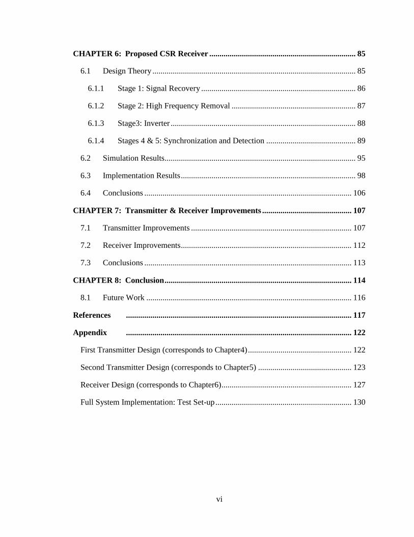
TABLE OF CONTENTS
List of Tables ................................................................................................................. vii
List of Figures ................................................................................................................ viii
List of Abbreviations ...................................................................................................... xii
Acknowledgments .......................................................................................................... xiv
Abstract ................................................................................................................. xv
CHAPTER 1: Introduction ............................................................................................. 1
1.1 Motivation ............................................................................................................ 1
1.2 Thesis Outline ...................................................................................................... 3
CHAPTER 2: Background of UWB ............................................................................... 5
2.1 UWB Definition and Regulations ........................................................................ 5
2.2 Types of UWB Transmission ............................................................................. 10
2.2.1 Multi-band ODFM UWB ............................................................................ 11
2.2.2 Impulse-Radio UWB .................................................................................. 13
2.3 The IR-UWB Pulse ............................................................................................ 14
2.3.1 Pulse Spectral Bandwidth ........................................................................... 14
2.3.2 Pulse Spectral Amplitude ............................................................................ 15
2.3.3 Pulse Shape ................................................................................................. 15
2.4 Advantages of IR-UWB Technology ................................................................. 18
2.4.1 Large Capacity and High Data-Rate ........................................................... 18
2.4.2 Flexibility in Data Rate versus Transmit Distance ..................................... 19
2.4.3 Low Interference and Low Probability of Detection/Interception .............. 19
2.4.4 Multipath Immunity .................................................................................... 20
v
2.5 Applications ....................................................................................................... 21
CHAPTER 3: Introduction to Code-Shifted Reference (CSR) .................................. 23
3.1 Previous Implementation Schemes for IR-UWB ............................................... 23
3.1.1 Rake Receiver ............................................................................................. 23
3.1.2 Transmit Reference Receiver ...................................................................... 25
3.1.3 Frequency Shifted Reference ...................................................................... 27
3.2 Code-Shifted Reference (CSR) .......................................................................... 28
3.2.1 Differential Code-Shifted Reference (DCSR) ............................................ 31
3.3 Performance Comparison ................................................................................... 35
CHAPTER 4: First Proposed CSR Transmitter ......................................................... 43
4.1 Design Theory .................................................................................................... 43
4.1.1 Stage1: Pulse Generation ............................................................................ 44
4.1.2 Stage 2: Pulse Gating .................................................................................. 47
4.1.3 Stage 3: Signal Coding ................................................................................ 49
4.2 Simulation Results .............................................................................................. 50
4.3 Implementation Results ...................................................................................... 55
4.4 Conclusions ........................................................................................................ 60
CHAPTER 5: Proposed CSR Transmitter .................................................................. 62
5.1 Design Theory .................................................................................................... 62
5.1.1 Stage1: Pulse Generator .............................................................................. 63
5.1.2 Stage2: Amplitude Modulation ................................................................... 64
5.1.3 Stage3: Gate Pulse ...................................................................................... 65
5.2 Simulation Results .............................................................................................. 68
5.3 Implementation Results ...................................................................................... 76
5.4 Conclusions ........................................................................................................ 83
vi
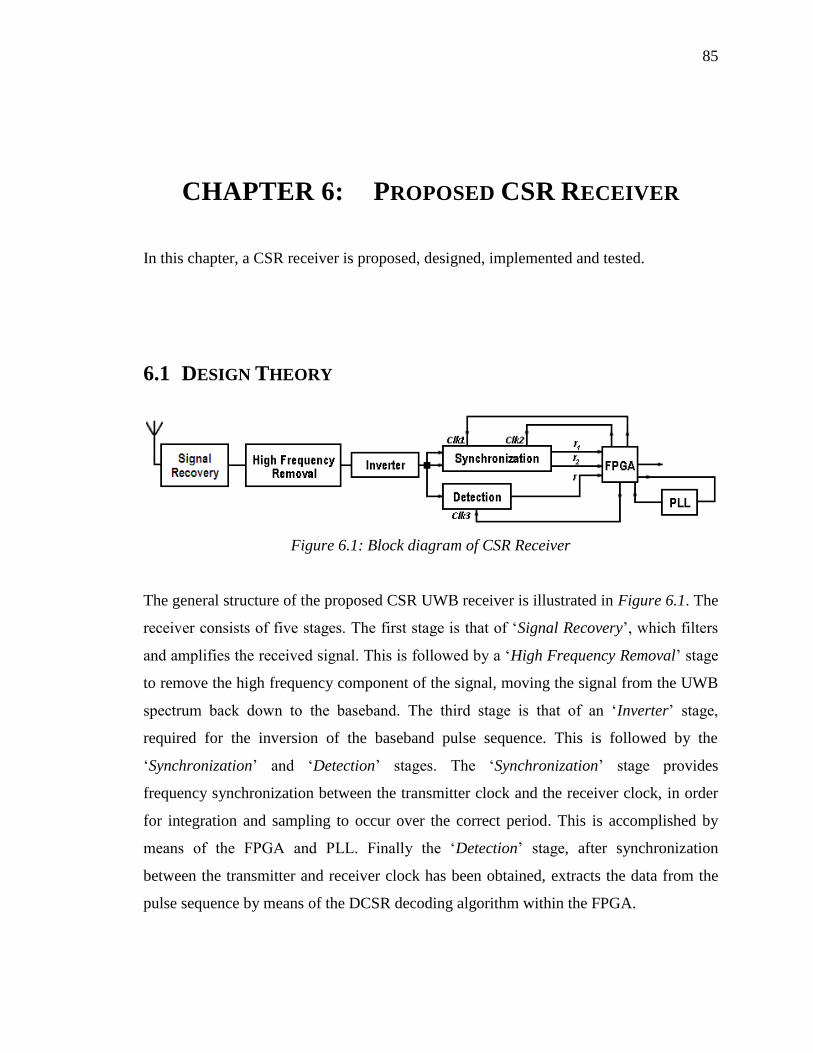
CHAPTER 6: Proposed CSR Receiver ........................................................................ 85
6.1 Design Theory .................................................................................................... 85
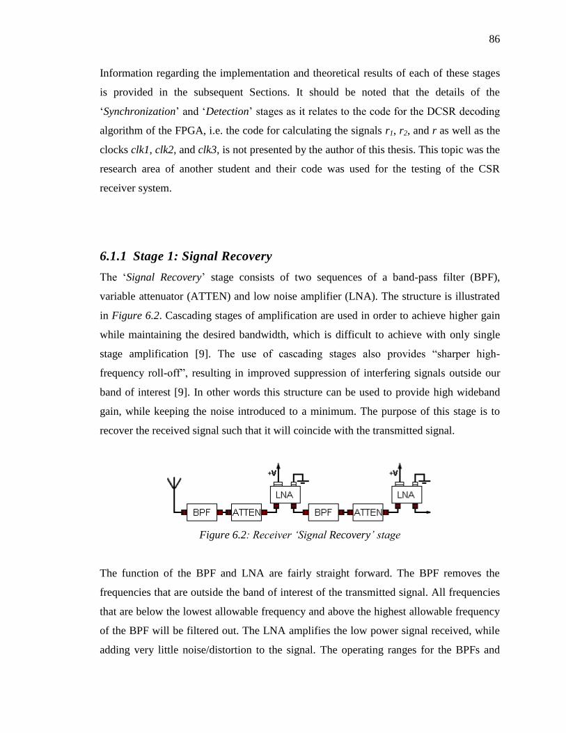
6.1.1 Stage 1: Signal Recovery ............................................................................ 86
6.1.2 Stage 2: High Frequency Removal ............................................................. 87
6.1.3 Stage3: Inverter ........................................................................................... 88
6.1.4 Stages 4 & 5: Synchronization and Detection ............................................ 89
6.2 Simulation Results .............................................................................................. 95
6.3 Implementation Results ...................................................................................... 98
6.4 Conclusions ...................................................................................................... 106
CHAPTER 7: Transmitter & Receiver Improvements ............................................ 107
7.1 Transmitter Improvements ............................................................................... 107
7.2 Receiver Improvements .................................................................................... 112
7.3 Conclusions ...................................................................................................... 113
CHAPTER 8: Conclusion ............................................................................................ 114
8.1 Future Work ..................................................................................................... 116
References ............................................................................................................... 117
Appendix ............................................................................................................... 122
First Transmitter Design (corresponds to Chapter4) ................................................... 122
Second Transmitter Design (corresponds to Chapter5) .............................................. 123
Receiver Design (corresponds to Chapter6) ................................................................ 127
Full System Implementation: Test Set-up ................................................................... 130
vii
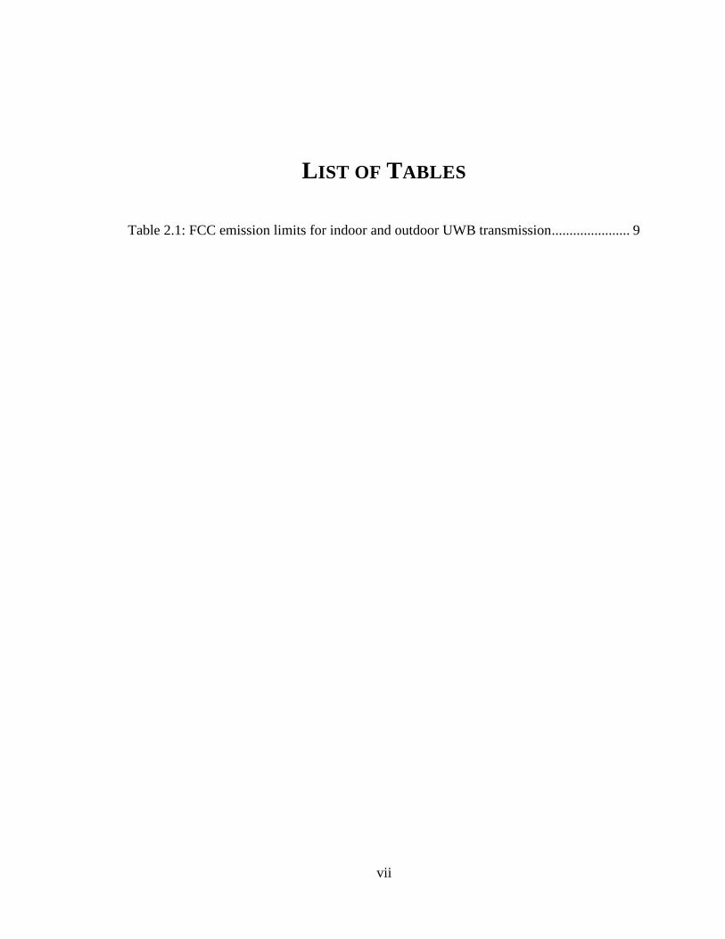
LIST OF TABLES
Table 2.1: FCC emission limits for indoor and outdoor UWB transmission ...................... 9
viii
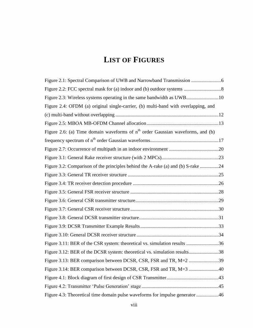
LIST OF FIGURES
Figure 2.1: Spectral Comparison of UWB and Narrowband Transmission ........................ 6
Figure 2.2: FCC spectral mask for (a) indoor and (b) outdoor systems .............................. 8
Figure 2.3: Wireless systems operating in the same bandwidth as UWB.......................... 10
Figure 2.4: OFDM (a) original single-carrier, (b) multi-band with overlapping, and
(c) multi-band without overlapping ................................................................................... 12
Figure 2.5: MBOA MB-OFDM Channel allocation .......................................................... 13
Figure 2.6: (a) Time domain waveforms of nth
order Gaussian waveforms, and (b)
frequency spectrum of nth
order Gaussian waveforms ....................................................... 17
Figure 2.7: Occurrence of multipath in an indoor environment ........................................ 20
Figure 3.1: General Rake receiver structure (with 2 MPCs).............................................. 23
Figure 3.2: Comparison of the principles behind the A-rake (a) and (b) S-rake ............... 24
Figure 3.3: General TR receiver structure ......................................................................... 25
Figure 3.4: TR receiver detection procedure ..................................................................... 26
Figure 3.5: General FSR receiver structure ....................................................................... 28
Figure 3.6: General CSR transmitter structure................................................................... 29
Figure 3.7: General CSR receiver structure ....................................................................... 30
Figure 3.8: General DCSR transmitter structure ................................................................ 31
Figure 3.9: DCSR Transmitter Example Results ............................................................... 33
Figure 3.10: General DCSR receiver structure .................................................................. 34
Figure 3.11: BER of the CSR system: theoretical vs. simulation results .......................... 36
Figure 3.12: BER of the DCSR system: theoretical vs. simulation results ........................ 38
Figure 3.13: BER comparison between DCSR, CSR, FSR and TR, M=2 ........................ 39
Figure 3.14: BER comparison between DCSR, CSR, FSR and TR, M=3 ........................ 40
Figure 4.1: Block diagram of first design of CSR Transmitter .......................................... 43
Figure 4.2: Transmitter „Pulse Generation‟ stage .............................................................. 45
Figure 4.3: Theoretical time domain pulse waveforms for impulse generator .................. 46
ix
Figure 4.4: Concept of Pulse Gating in the time domain ................................................... 47
Figure 4.5: Transmitter „Gated Pulse‟ stage ...................................................................... 47
Figure 4.6: Theoretical time domain response of the „Gated Pulse‟ stage ........................ 48
Figure 4.7: Concept of pulse coding by the VGA.............................................................. 49
Figure 4.8: Simulation schematic of „Pulse Generation‟ and „Gated Pulse‟ stages ........... 51
Figure 4.9: Simulation results of „Pulse Generation‟ stage ............................................... 52
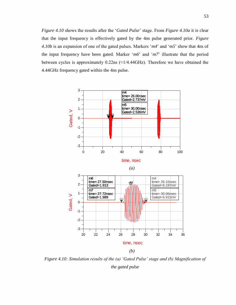
Figure 4.10: Simulation results of the (a) „Gated Pulse‟ stage and (b) Magnification
of the gated pulse ............................................................................................................... 53
Figure 4.11: Spectral response of the simulated pulse results against FCC indoor
mask ................................................................................................................................... 54
Figure 4.12: Full Schematic of the first Transmitter design .............................................. 56
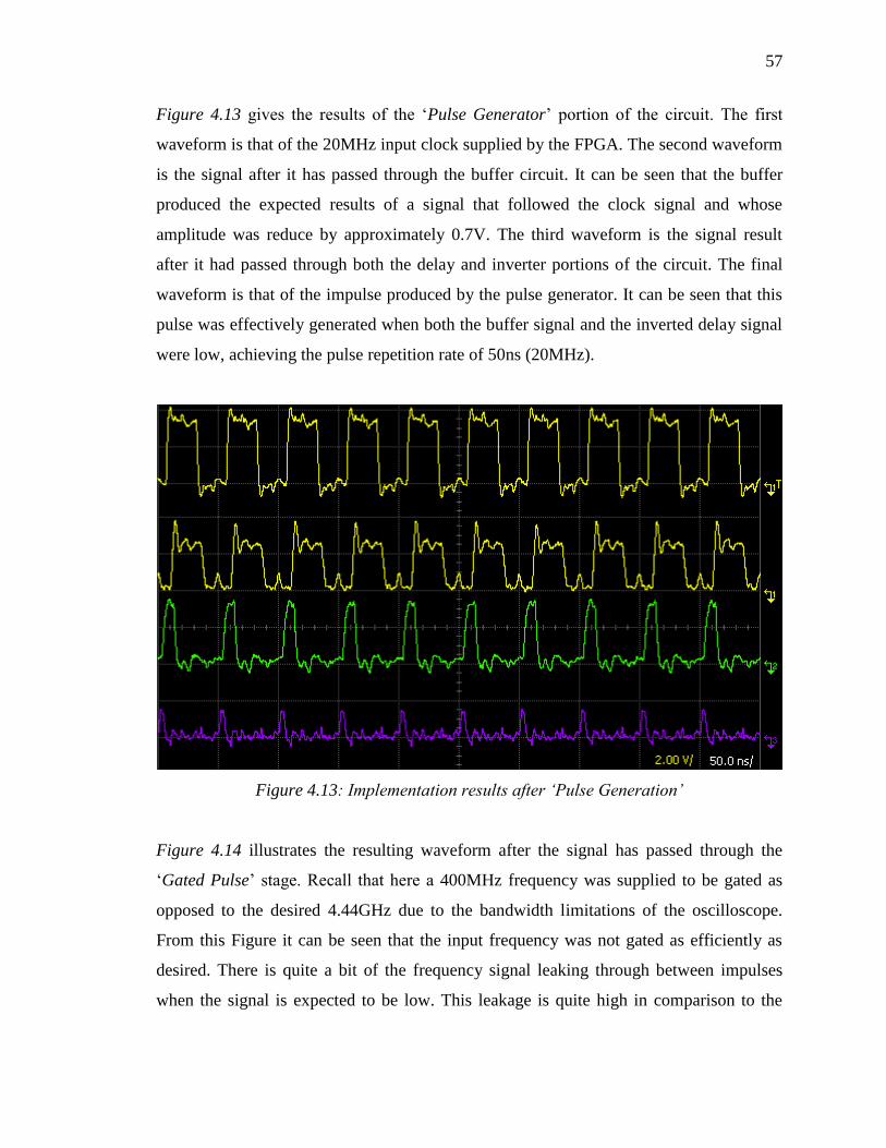
Figure 4.13: Implementation results after „Pulse Generation‟ ........................................... 57
Figure 4.14: Implementation results after „Pulse Gating‟ .................................................. 58
Figure 4.15: Implementation results after VGA ................................................................ 58
Figure 4.16: Implementation results after VGA with clock rate of (a) 5MHz and
(b)100KHz ......................................................................................................................... 60
Figure 5.1: Block Diagram of CSR Transmitter ................................................................ 62
Figure 5.2: Revised transmitter „Pulse Generation‟ stage .................................................. 63
Figure 5.3: Revised transmitter „Amplitude Modulation‟ stage ........................................ 64
Figure 5.4: General structure of the Inverting Op-amp ..................................................... 65
Figure 5.5 Example of combined amplitude modulated pulse sequence ........................... 65
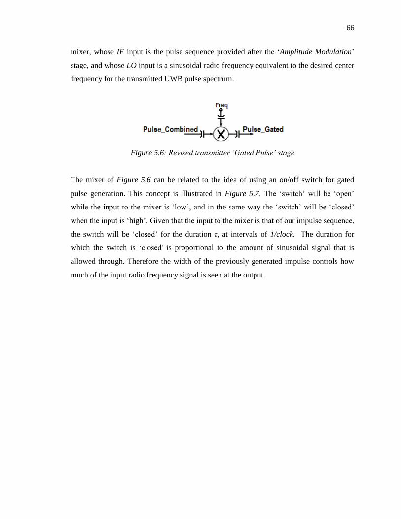
Figure 5.6: Revised transmitter „Gated Pulse‟ stage .......................................................... 66
Figure 5.7: (a) Concept and (b) Application of gating signal in time domain ................... 67
Figure 5.8: Simulation schematic of revised CSR Transmitter ......................................... 68
Figure 5.9: Simulation results of (a) „Pulse Generator 1‟ and (b) „Pulse Generator 2‟ ..... 69
Figure 5.10: Amplification Method1 to produce 3:1 ratio ................................................. 70
Figure 5.11: Simulation results of „Amplitude Modulation‟ stage of the transmitter –
Amplification Method1 ...................................................................................................... 71
Figure 5.12: Amplification Method2 to produce 3:1 ratio ................................................. 72
Figure 5.13: Simulation results of „Amplitude Modulation‟ stage of the transmitter –
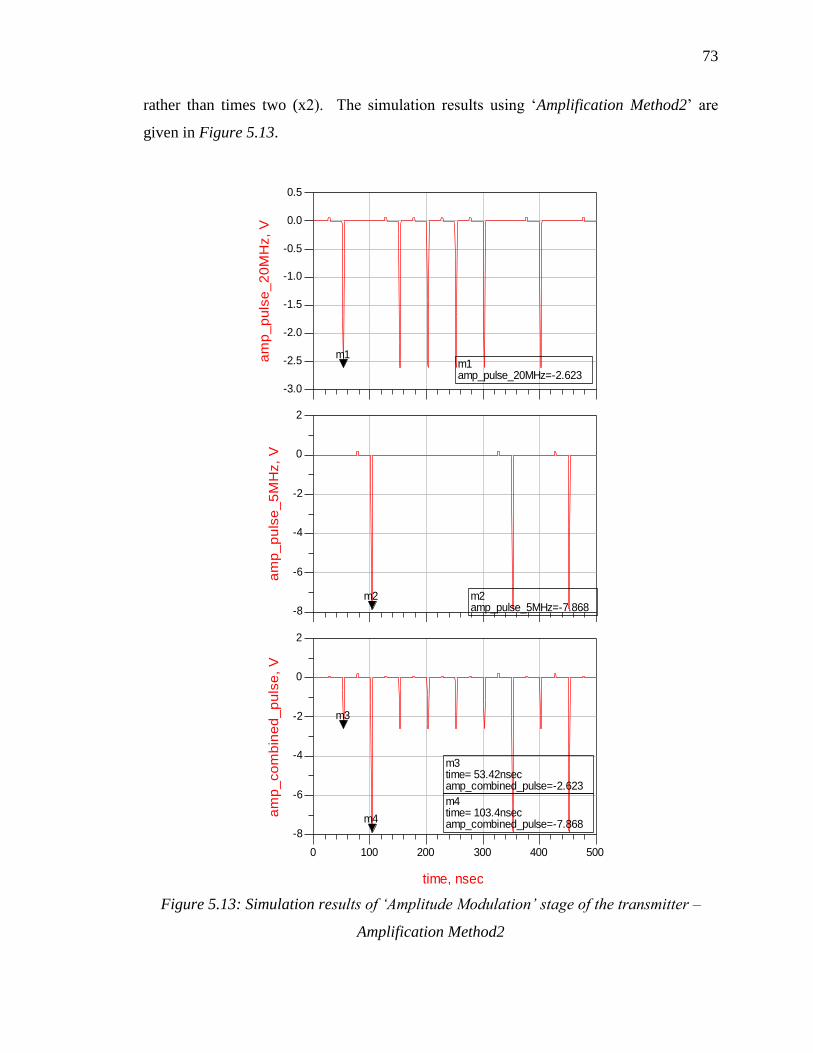
Amplification Method2 ...................................................................................................... 73
x
Figure 5.14 : Simulation results of the (a) „Gated Pulse‟ stage and (b) Magnification
of the gated pulse ............................................................................................................... 75
Figure 5.15: Full design of the Transmitter implementation ............................................. 77
Figure 5.16: Oscilloscope results of Board1 after each stage of – Pulse Generation ........ 79
Figure 5.17: Oscilloscope results of „Pulse Generator 1‟ and „Pulse Generator 2‟
impulses expanded ............................................................................................................. 80
Figure 5.18: Oscilloscope results of Board2 – Amplitude Modulation ............................. 80
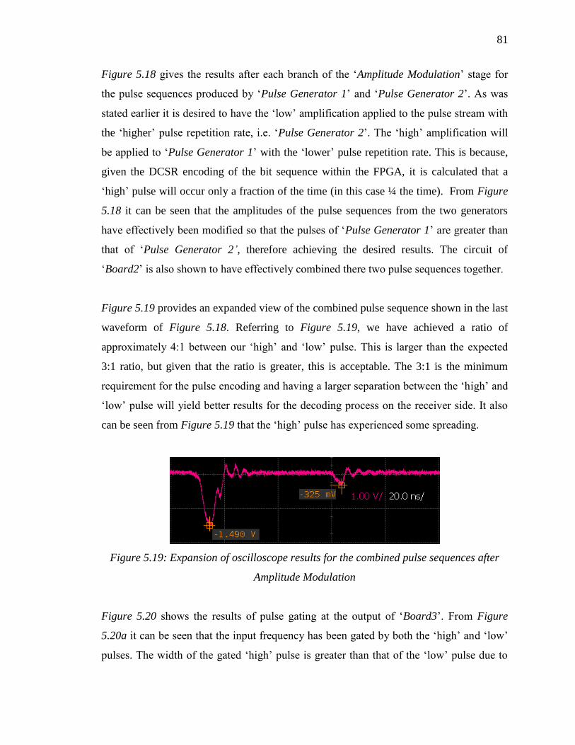
Figure 5.19: Expansion of oscilloscope results for the combined pulse sequences
after Amplitude Modulation .............................................................................................. 81
Figure 5.20: Oscilloscope results of Board3 – Pulse Gating (a) 100ns expansion, (b)
20ns expansion, (c) 1ns expansion ..................................................................................... 82
Figure 6.1: Block diagram of CSR Receiver ..................................................................... 85
Figure 6.2: Receiver „Signal Recovery‟ stage ................................................................... 86
Figure 6.3: Theoretically expected results after „Signal Recovery‟ stage ......................... 87
Figure 6.4: Receiver „High Frequency Removal‟ stage ..................................................... 88
Figure 6.5: Theoretically expected results after the „High Frequency Removal‟ stage ..... 88
Figure 6.6: Receiver „Inverter‟ stage ................................................................................. 89
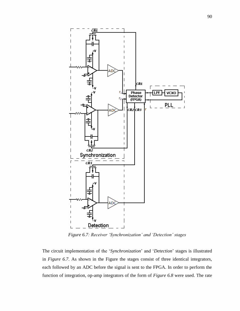
Figure 6.7: Receiver „Synchronization‟ and „Detection‟ stages ........................................ 90
Figure 6.8: Concept of the op-amp integrator .................................................................... 91
Figure 6.9: Correct vs. incorrect integration ...................................................................... 92
Figure 6.10: Integration Signals ......................................................................................... 92
Figure 6.11: Theoretical clock and integration signals: clk1 and clk2 .............................. 93
Figure 6.12: Synchronization concept ............................................................................... 94
Figure 6.13: Theoretical clock and integration signals: all clocks ..................................... 95
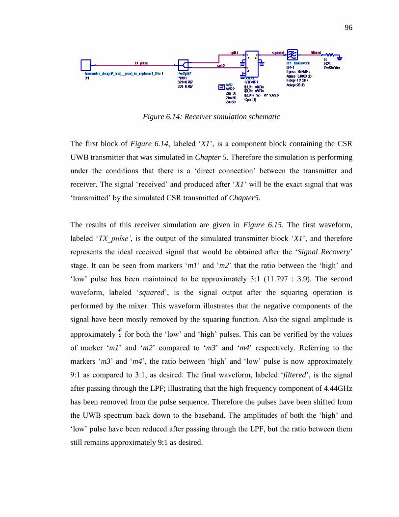
Figure 6.14: Receiver simulation schematic ...................................................................... 96
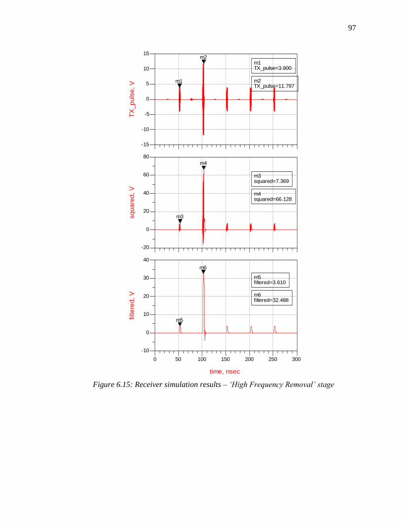
Figure 6.15: Receiver simulation results – „High Frequency Removal‟ stage .................. 97
Figure 6.16: CSR Receiver implementation schematic ..................................................... 99
Figure 6.17: Receiver implementation result - after the „Signal Recovery‟ stage ........... 100
Figure 6.18: Transmitter implementation result - after the „Gated Pulse‟ stage .............. 100
Figure 6.19: Receiver encoded pulse sequence – after „High Frequency Removal‟
stage (a) 100ns scale and (b) 20ns scale .......................................................................... 101
xi
Figure 6.20: Transmitter encoded pulse sequence – after „Amplitude Modulation‟
stage ................................................................................................................................. 102
Figure 6.21: Results before and after „Inverter‟ stage ..................................................... 103
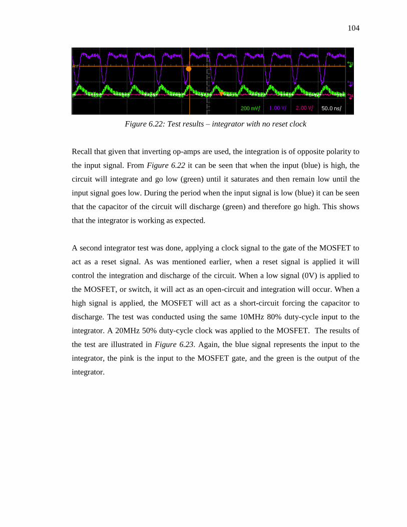
Figure 6.22: Test results – integrator with no reset clock ................................................ 104
Figure 6.23: Test results – integrator with reset clock ..................................................... 105
Figure 7.1: „Amplitude Modulation‟ stage results before improvements ........................ 108
Figure 7.2: „Amplitude Modulation‟ stage test: „high‟ pulse branch
(R1=R2=100Ohm) ............................................................................................................ 108
Figure 7.3: Improved „Amplified Modulation‟ stage results (a) „high‟ and „low‟ pulse
sequences and (b) enlarged view ..................................................................................... 109
Figure 7.4: Improved „Amplified Modulation‟ stage results (a) combined pulse
sequence and (b) enlarged view ....................................................................................... 110
Figure 7.5: Results after added variable attenuator (a) combined pulse sequence and
(b) enlarged view ............................................................................................................. 112
Figure 7.6: „High Frequency Removal‟ stage results after improvements (a) pulse
sequence and (b) enlarged view ....................................................................................... 113
Figure A.1: Top-layer PCB layout of the first design of the CSR Transmitter ............... 122
Figure A.2: Top-layer PCB layout of „Pulse Generation‟ stage of the second design
of the CSR Transmitter .................................................................................................... 123
Figure A.3: Top-layer PCB layout of „Amplitude Modulation‟ stage of the second
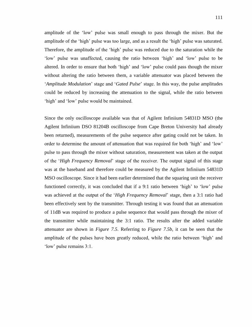
design of the CSR Transmitter ......................................................................................... 124
Figure A.4: Top-layer PCB layout of „Gated Pulse‟ stage of the second design of the
CSR Transmitter .............................................................................................................. 125
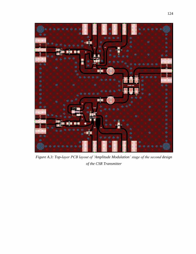
Figure A.5: Top-layer PCB layout of BPF and Antenna of the second design of the
CSR Transmitter .............................................................................................................. 126
Figure A.6: Top-layer PCB layout of „Inverter‟ stage of the CSR Receiver ................... 127
Figure A.7: Top-layer PCB layout of Integrators of the CSR Receiver .......................... 128
Figure A.8: Top-layer PCB layout of ADCs of the CSR Receiver ................................. 129
Figure A.9: Picture of test set-up of CSR Transmitter and Receiver ............................... 130
xii
LIST OF ABBREVIATIONS
AC Alternating Current
ADC Analog to Digital Converter
ADS Advanced Design Systems
ATTEN Attenuator
AWGN Additive White Gaussian Noise
BER Bit Error Rate
BJT Bipolar Junction Transistor
BPF Band-pass Filter
BW Bandwidth
CE Consumer Electronic
CMOS Complementary Metal–Oxide–Semiconductor
CSR Code-Shifted Reference
DC Direct Current
DCSR Differential Code-Shifted Reference
EIRP Equivalent Isotopic Radiated Power
FCC Federal Communications Commission
FPGA Field-programmable Gate Array
FSR Frequency-Shifted Reference
GPS Global Positioning System
HDR High data-rate
IC Integrated Circuit
IF Intermediate Frequency
IR Impulse-Radio
ISI Inter-Symbol Interference
ISM Industry, Scientific, and Medical (systems)
LDR Low data-rate
xiii
LNA Low Noise Amplifier
LO Local Oscillator
LPF Low-pass filter
MB Multi-band
MBOA Multiband OFDM Alliance
MPC Multipath Component
OFDM Orthogonal Frequency Division Multiplexing
PAPR Peak to Average Power Ratio
PC Personal Computer
PCB Printed Circuit Board
PLL Phase Lock Loop
PPR Pulse Repetition Rate
PSD Power Spectral Density
RF Radio Frequency
RMS Root Mean Square
S-FSR Slightly Frequency-Shifted Reference
SMT Surface-mount
SNR Signal-to-Noise Ratio
SRD Step Recovery Diode
TR Transmit Reference
UWB Ultra Wideband
VCXO Voltage Control Crystal Oscillator
VGA Variable Gain Amplifier
WLAN Wireless Local Area Network
xiv
ACKNOWLEDGMENTS
First and foremost, I want to give thanks to God. He has given me the strength and
courage to reach my goals, and surrounded me with wonderful family, friends and peers.
Through Him, so many obstacles have been overcome and I have been able to achieve
things that I would have otherwise thought impossible.
I would like to thank my Supervisor Dr. Zhizhang Chen for giving me the opportunity to
research this topic. I truly appreciate his encouragement to learn as much as I can, and for
his continued guidance and support in the completion of this project. I would also like to
thank Dr. Hong Nie for agreeing to be my co-supervisor, and for his useful discussions
and guidance.
I would like to extend my gratitude to InNova Corp of Nova Scotia Government of
Canada for their financial support. Also thanks to Cape Breton University for kindly
allowing us to borrow their oscilloscope.
I would like to thank the members of the RF and Wireless Lab for their support and
kindness. Thanks to all the staff and professors within the ECE Department for enriching
my experience at Dalhousie. Thanks to Dr. Munir Tarar for his technical advice and
guidance. Also to Chen Wie, for working with me on this project, providing the
programming of the FPGA to perform the coding and decoding of the DSCR signals.
Finally, I would like to thank my parents, Daniel and Clara Lowe, and my sister Jenai, for
all their love, support, patience, and continued encouragement throughout my degree.
This thesis is dedicated to them.
xv
ABSTRACT
The objective of this thesis is to present the design, implementation and testing of a
Transmitter and Receiver for the use of the emerging Code-Shifted Reference (CSR)
scheme for Impulse-Radio Ultra-Wideband (IR-UWB) systems.
The transmitter is shown to generate impulses of duration 4ns at repetition rates of
20MHz. In order to avoid any interference with WLAN operating at 5GHz, it was
decided to have the UWB system operate in the lower half of the UWB spectrum, from 3-
5GHz, with a center frequency of 4.44GHz. After gating, the spectrum will consist of two
250MHz bands located at 4.44GHz+250MHz and 4.44GHz-250MHz, i.e. a 500MHz
bandwidth centered at 4.44GHz; therefore meeting the 500MHz bandwidth requirement
of UWB transmission. The impulses are encoded by means of amplitude modulation,
according to information provided by the FPGA based on the differential CSR algorithm.
The transmitted coded-impulse-sequence is recovered by means of the CSR receiver,
based on the general structure outlined in [1]. Band-pass filtering is performed to remove
noise and interferences outside of the desired frequency band. Squaring and low-pass
filtering is to remove the 4.44GHz, ultimately recovering the baseband signal originally
produced by the impulse generator of the transmitter (with the amplitudes of the impulses
being squared their original value). Integration is to detect the energy of the recovered
signal. The FPGA performs the clock synchronization between the receiver clock and the
transmitter clock by means of a phase-lock-loop (PLL). The data sequence is then
extracted from the signal by means of the differential CSR algorithm.
1
CHAPTER 1: INTRODUCTION
1.1 MOTIVATION
Traditionally, the field of wireless communication has been dominated by transmission
schemes based on conventional narrowband technology. The challenge faced by
narrowband transmission results from its limited bandwidth, which has the direct effect of
limiting the transmission capacity. Therefore narrowband systems are unable to
accommodate the increasing need of higher data-rates in wireless communication
applications.
Providing a solution to the problem of bandwidth limitation, Ultra-wideband (UWB)
technology has recently received a significant amount of attention in the field of wireless
communication. Although UWB is not a new concept, having been used for several years
for military applications, the Federal Communications Commission‟s (FCC) approval of
an unlicensed UWB spectrum for wireless communications has opened up new potentials
in this field, sparking the interest of both industry and academia.
In comparison to narrowband transmission, UWB technology spreads the signal over a
very wide range of frequencies by means of transmitting ultra-short duration pulses on
the order of nanoseconds. This enables transmission speeds of several hundred Mbps,
accommodating the high data-rate demands of current and future wireless systems. In
addition to the advantage of higher data-rates, the reason for UWB‟s popularity in the
wireless field lies in the many other benefits it offers, including low-cost, low transmit
power, low complexity, low power consumption, and low probability of detection and
interference.
2
Over the years, several implementation schemes for impulse-radio (IR) UWB systems
have been presented. Most notably, these include methods such as Transmit Reference
(TR) and Frequency-Shifted Reference (FSR), which have overcome the complexity of
channel estimation by transmitting reference pulses to be used as a template for extracting
the data pulse. In these methods, this reference pulse is separated from the data pulse by a
shift in time and frequency respectively.
Recently, the scheme of Code-Shifted Reference (CSR) has been proposed for IR-UWB
transmission [1]. In the proposed CSR scheme, rather than being separated by time (TR)
or by frequency (FSR), the reference and data pulse sequences are separated by codes [1].
The CSR scheme overcomes the technical challenges encountered by other UWB
systems, given that it does not require explicit channel estimation, a wideband delay
element, or separation of reference and data pulse by analog carriers; as a result, it has
reduced system complexity, and has been found to achieve better performance than the
previous schemes [2].
Papers such as [2] have been published, analyzing the theoretical performance of CSR
transmission in comparison to existing schemes such as the Rake Receiver, TR and FSR.
However, to the best of our knowledge, there has yet to be research done in terms of the
design and testing of a transceiver implementing and verifying the proposed Code-Shifted
Reference (CSR) scheme. Therefore, this thesis aims to provide a design for the
implementation of the transmitter and receiver for the CSR IR-UWB system, as well as
provide test results and discussion on the performance of this system.
3
1.2 THESIS OUTLINE
The organization of this thesis is as follows:
Chapter 2 provides a brief background to Ultra-wideband technologies. The definition
and regulations of UWB transmission as set by the FCC are presented. This is followed
by a discussion on the two types of UWB transmission, namely Impulse-Radio (IR) and
Multi-band Orthogonal frequency-division multiplexing (MB-OFDM). Given that this
thesis utilizes the method of Impulse-Radio transmission, emphasis on the characteristics
of IR transmission is given; such as spectral amplitude, bandwidth and pulse shape. This
Chapter also covers the advantages of IR-UWB technology, focusing on its ability to
achieve high data-rates, the flexibility and trade-off between transmission distance and
data-rate, as well as features of multipath immunity and low probability of detection and
interception. Finally, a brief section is given on the applications of UWB technology, in
specific, applications of high data-rate, short transmission distance (as this is the target
for the system presented in this thesis).
Chapter 3 gives a brief introduction to schemes for implementing IR-UWB. This includes
the methods of Rake Receiver, Transmit Reference (TR), Frequency-Shift Reference
(FSR), and emerging Code-Shifted Reference (CSR). A brief discussion is given for each
method, concluded by a section providing a performance comparison between CSR and
the previous methods of Rake, TR and FSR.
Chapter 4 provides the first proposed CSR transmitter as was presented in [3]. This
design was later altered, as it was found after implementation the system did not function
as efficiently as desired, or as was expected, based on the simulation results. The design
theory behind the function of the transmitter is presented, as well as the simulation
results. The results obtained after implementation of the circuit are provided and
compared to the simulation results. The overall performance of the transmitter is then
discussed.
4
Chapter 5 presents the redesigned CSR transmitter. Design theory behind the function of
each of the stages of the transmitter is given. The simulation results are presented and
compared with the results obtained from the previous transmitter design (given in
Chapter 4). The implementation results of this transmitter are also presented. These
results are discussed and compared with the implementation results of the previous
transmitter. The results are also compared with its own simulation results to verify that
the performance was as expected.
Chapter 6 presents the CSR Receiver. As in the previous two chapters, the design theory
of the receiver is given, followed by the simulation and implementation results obtained.
Comparison and discussion is made between the expected (simulated) results and the
results obtained after implementation and testing.
Chapter 7 provides some improvements that were made to the systems after initial testing
had been performed on the CSR transmitter and receiver. These improvements were
made to enhance the performance of the system, providing the optimal ratio between
„high‟ and „low‟ pulse so that decoding performed by the receiver would have a better
performance. The test results of the changes made to the implemented boards for both
transmitter and receiver are presented and discussed in this Chapter.
Chapter 8 provides a conclusion to the thesis. This Chapter presents an overall summary
of the thesis as well as some improvements that can be made to the system in the future.
Further future work for the system is provided.
References are given at the end of the thesis; as well as an Appendix containing the PCB
layouts for the transmitter and receiver boards, and photos of the test set-up of the
implemented system.
5
CHAPTER 2: BACKGROUND OF UWB
2.1 UWB DEFINITION AND REGULATIONS
The FCC has defined a UWB system as any wireless scheme whose signals have a -10dB
fractional bandwidth (Bf) at least 20% higher than its center frequency (fc), or a -10dB
absolute bandwidth (BW) greater than or equal to 500MHz [6]. The -10dB absolute
bandwidth is defined as the frequency band bound by fh and fl, which are the upper and
lower frequency points 10dB below the highest radiated power of the complete
transmission system (including the antenna). The fractional bandwidth (Bf) can be
expressed as [6]:
(2.1)
where the center frequency fc is defined as the average of fl and fh:
(2.2)
The definitions of fractional and absolute bandwidth are illustrated in Figure 2.1. This
Figure clearly illustrates the comparison of fractional bandwidth between UWB and
traditional narrowband communications. It can be seen that UWB transmission offers a
spectral fractional bandwidth of twenty times that of traditional narrowband transmission.
6
Figure 2.1: Spectral Comparison of UWB and Narrowband Transmission [4]
Figure 2.1 also illustrates that UWB transmission has a far lower power spectral density
(PSD) than narrowband. The approximate value of the PSD of a system is defined as:
(2.3)
where P is the transmit power (Watts) and BW is the absolute bandwidth (Hz); therefore
PSD is measured in W/Hz. Given this equation, it can be determined that for a fixed
amount of power, we can either transmit with a large PSD value over a small frequency
bandwidth or a small PSD value over a larger frequency bandwidth.
The reason that FCC specifies a very low PSD is due to the fact that UWB covers
extremely large bandwidth that overlaps the transmission spectrums of many existing
wireless narrowband systems. This poses a danger of signal interference between these
systems and UWB transmissions. In order to avoid interference between UWB and other
wireless systems, the FCC specified that the UWB maximum equivalent isotopic radiated
power (EIRP) spectral density be -41.3dBm/MHz. The EIRP is defined as the theoretical
7
amount of power that the transmitter will emit, with the assumption that the transmitter is
radiating equally in all directions.
In the Report and Order issued in 2002 [6], the FCC allocated two separate frequency
bands for UWB transmission: the first is the DC-960MHz band, mainly for lower data-
rate transmission (radar applications) [5] and the second is the 3.1-10.6GHz band
(frequency band of interest for this research), reserved mainly for UWB communication
systems. A spectral mask was defined for both indoor and outdoor UWB transmissions.
These masks are given in Figure2.2a and Figure2.2b, respectively.
For a UWB system that utilizes the entire 7.5GHz of the available spectral band, the
maximum allowable transmit-power would be approximately 0.56mW. Given these
extreme limitations on the transmission power, UWB systems can be seen to operate at
the noise floor of existing wireless narrowband systems, and therefore does not interfere
with their performance as the systems will see the UWB transmission as merely noise.
8
(a)
(b)
Figure 2.2: FCC spectral mask for (a) indoor and (b) outdoor systems [4]
9
Figure 2.2 indicates that emission limits within the UWB spectrum are varied between
specific frequency bands. These emission limits can be summarized in Table 2.1 below.
Table 2.1: FCC emission limits for indoor and outdoor UWB transmission [7]
Frequency (MHz) Indoor
EIRP (dBm/MHz)
Outdoor
EIRP (dBm/MHz)
0-960 -41.3 -41.3
960-1610 -75.3 -75.3
1610-1990 -53.3 -63.3
1990-3100 -51.3 -61.3
3100-10600 -41.3 -41.3
Above 1060 -51.3 -61.3
It should be noted that the maximum allowable power emissions between the frequency
band 0.96-1.61GHz is extremely low (-75.3dBm/MHz). The reason for avoiding
frequencies in this band is illustrated in Figure 2.3, i.e. to avoid interference with the
many existing systems that operate at those frequencies, such as global positioning
systems (GPS), cellular and military usage. This can also be considered a safety measure
given that interference between systems such as aviation/military and GPS can prove
detrimental. Therefore, the range of operation for UWB communications is specified to
be between 3.1-10.6GHz, where the most probable interference is with Wireless Local
Area Network (WLAN) systems. Even so, as a further precaution, many researchers have
chosen to also avoid the frequencies occupied by WLAN. Therefore transmission can be
chosen to operate in either the lower band (3.1-5GHz) or upper band (6-10.6GHz) of the
7.5GHz allocated for UWB communications [9].
10
Figure 2.3: Wireless systems operating in the same bandwidth as UWB [8]
2.2 TYPES OF UWB TRANSMISSION
In general, there are two common forms in which UWB signals are transmitted. These
two forms are referred to as Multi-band Orthogonal Frequency Division Multiplexing
(OFDM) and Impulse-Radio (IR) UWB. The approach chosen for this project was that of
Impulse-Radio UWB. A brief explanation of each method is provided in the following
subsections. Further detail regarding the advantages and characteristics of Impulse-Radio
is provided in the following sub-sections, Sections 2.3-2.5, of this Chapter.
11
2.2.1 Multi-band ODFM UWB
Multi-band OFDM (MB-OFDM) UWB employs at least two or more frequency bands,
where each band complies with the FCC regulation that BW≥500MHz. In this way MB-
OFDM aims to make use of the allotted UWB spectrum while adhering to the FCC
requirements for minimum bandwidth. [10]
MB-OFDM can be described as the “parallel transmission of N symbols”, where each
symbol is used to modulate a different sub-carrier frequency, fm [12]. In order for the N
symbols to be effectively resolved by the receiver, orthogonality must be maintained
between sub-carriers [12]. To achieve this, the equal spacing between sub-carriers must
be at least Δf in the spectral domain, where Δf=1/Ts and Ts is the time taken to transmit
each symbol [12]. Figure 2.4 illustrates the instances where the sub-carriers are spaced at
frequencies of Δf (Figure 2.4b) resulting in overlapping sub-carriers, and at 2Δf (Figure
2.4c) resulting in sub-carriers that do not overlap. In both cases orthogonality is obtained
between signals, due to the fact that the peak of one sub-carrier occurs when the other
sub-carriers are at zero.
12
(a)
(b)
(c)
Figure 2.4: OFDM (a) original single-carrier, (b) multi-band with overlapping [7], and
(c) multi-band without overlapping [7]
13
An alliance known as the MBOA (Multiband OFDM Alliance), proposed that the
available 7.5GHz for UWB transmission be divided into 14 non-overlapping sub-bands
of 528MHz [13]. These sub-bands are grouped into five Channels as shown in Figure
2.5. Channel 1, containing the first three sub-bands, is considered mandatory for UWB
transmission. The other Channels are optional; therefore certain sub-bands can go unused
to avoid interference with existing systems [13]. It should be noted that this is the MB-
OFDM UWB plan for North America. This channel allocation differs in places such as
Europe and Japan. [14]
Figure 2.5: MBOA MB-OFDM Channel allocation [14]
2.2.2 Impulse-Radio UWB
The Impulse-Radio UWB (IR-UWB) method employs transmission by means of ultra
short duration pulses on the order of nanoseconds. The width of these pulses determines
the bandwidth the transmitted signal will occupy in the spectral domain. In this way a
single narrow pulse can occupy the entire UWB spectrum. The pulses do not carry any
information themselves, but are usually „encoded‟ by means of amplitude, position or
polarity modulation to represent the information to be transmitted. [10]
IR-UWB is discontinuous pulse transmission in time, where the UWB pulse sequence
transmitted has a very low duty-cycle. This has an advantage over continuous
transmission techniques in that the receiver is only required to function for a small
duration of the cycle. The impact of interference from a continuous source is reduced
14
with IR-UWB. This is due to the fact that the interference will only have relevance when
the receiver is trying to detect the signal. Given the very low duty-cycle, this is only for a
very small fraction of each period. Between periods, the receiver simply has to „listen‟ to
the channel as it waits for the next pulse. [10]
2.3 THE IR-UWB PULSE
In the case of IR-UWB, the pulse plays an extremely important role in signal
transmission, as the characteristics of the generated pulse determine the spectral
characteristics of the signal. Therefore in order to make best use of the spectral mask
provided by the FCC, the characteristics of the UWB pulse must be carefully chosen.
This Section will cover the importance of the generated pulse characteristics, and the
ways in which these time domain characteristics impact the spectral characteristics of the
transmitted signal.
2.3.1 Pulse Spectral Bandwidth
The duration, or width, of the pulse will determine the bandwidth of the signal in the
frequency domain. This is in relation to the fact that the inverse of the period of a signal
is equivalent to its bandwidth, and vice-versa. In the case of an impulse, the inverse of the
duration of the pulse, τ, is equivalent to its spectral bandwidth, BW. In general, as a rule
of thumb, it can be said that:
(2.4)
Given the above relation, it can be concluded that in order to achieve an extremely large
bandwidth, the pulse duration must be small. For this reason, the widths of UWB pulses
15
are designed to be on the order of nanoseconds in order to occupy spectral bandwidths of
500MHz up to several GHz.
2.3.2 Pulse Spectral Amplitude
The transmit power, limited by the FCC spectral mask to a maximum of -41.3dBm/MHz,
is dependent on the pulse repetition rate, PRR, (pulse/sec) and the amplitude of the pulses
in the time domain [16]. The element actually being limited by these factors is the
spectral amplitude of the signal such that:
(2.5)
where Vf is the spectral amplitude of the main lobe in the frequency domain, Vt is the
root-mean-square (RMS) amplitude of the pulse in the time domain, τ is the width of the
generated impulse, and T is the pulse rate (1/clock). [16]
Therefore, when considering the transmission of the pulse, if the PRR is low (i.e. T is
large) then the pulses can have higher amplitude in the time domain. If the pulse rate is
high, the pulses must have lower amplitudes in order to keep in accordance with the FCC
emission limits.
2.3.3 Pulse Shape
The shape of the pulse is a key factor in determining how the signal energy will occupy
the spectral domain, i.e. how effectively the pulse will make use of the allotted FCC
spectral mask. Therefore this topic has been of great interest in designing a UWB pulse
generator that will make the best use of the FCC spectral mask.
Generally, for IR transmission the shape of the pulse is not specifically defined. Any
pulse whose spectral response fits the FCC spectral mask can be used. Within literature,
pulse shapes used are typically the Gaussian pulse and its derivatives (e.g. monocycle,
16
doublet), Rayleigh monocycles, Manchester monocycles, or Hermite pulses [17]. Of
these listed, the most common pulse shape used in UWB transmission is that of the
Gaussian pulse due to its simplicity in generation.
Examples of the waveforms of a Gaussian pulse and its derivatives in both the time and
frequency domain are illustrated in Figure 2.6a and Figure2.6b respectively, taken from
[17]. From these Figures the spectral effects of changes made to the order (n) and the
width (tp) of the Gaussian pulse can be observed. First we will consider the effect of
changing the order of the Gaussian pulse, while fixing the pulse width to a constant value.
In this case we will refer to the spectral waveforms of Figure 2.6b, 2,tp2 and 5,tp2, where
„2‟ and „5‟ correspond to the order of the Gaussian pulse and tp2 corresponds to the width.
Comparing these two waveforms it can be seen that as the order of the Gaussian pulse is
increased, the spectrum is shifted towards a higher frequency range, while the bandwidth
of the spectrum remains relatively constant. We now consider the effect of changing the
pulse width while keeping the order of the Gaussian pulse constant. Comparing the
spectral waveforms of 2,tp2 and 2,tp1, where the width of the pulse tp2 is less than tp1,
shows that as the width of the pulse is decreased, the bandwidth is increased. Also, in this
case the spectrum is shifted slightly towards a higher frequency range. [17]
17
(a)
(b)
Figure 2.6: (a) Time domain waveforms of nth
order Gaussian waveforms, and (b)
frequency spectrum of nth
order Gaussian waveforms [17]
Of the derivatives of Gaussian pulses, most literature favors the Gaussian monocycle
(first derivative Gaussian) and Gaussian doublet (second derivative Gaussian) for UWB
systems [18-23]. These pulses are easily generated and have zero DC components [24].
Although these pulses have a zero DC component, their spectra still goes down to very
low frequencies, which are well below the minimum 3.1GHz of the UWB spectra. This is
illustrated in Figure2.6b, where the second order Gaussian doublet (n=2) does not have a
DC component, but the spectra starts at a very low frequency. Whether the spectra of the
doublet will be within the UWB spectral range depends on the width of the pulse. As
stated before, the shorter the pulse duration, the wider the frequency range it can span. If
the pulse width is small enough to span the UWB spectrum, some filtering is still
required to remove the lower frequency components.
Given the performance of nth
order Gaussian pulses illustrated in Figure2.6, papers such
as [25] and [26] have argued that using a higher order Gaussian pulse is more effective,
18
as they are able to satisfy the FCC mask without the filtering required for first and second
order Gaussian pulses. The only drawback is that it is more complicated to generate
higher order Gaussian pulses. Other papers have suggested means of modulating a
Gaussian-shaped pulse to shift the spectra upwards into the band of interest. For instance,
[24] suggests this can be achieved by modulating the pulse with a stable local oscillator
frequency. Others, such as [27] and [28], have suggested generating a sinusoidal
Gaussian monocycle or one of its derivatives by means of implementing a „gated
function‟. This will „gate‟ a sinusoidal input by means of some nanosecond pulse to
produce an impulse that resembles the shape of an nth
order Gaussian pulse.
2.4 ADVANTAGES OF IR-UWB TECHNOLOGY
There are several features of IR-UWB signals which make them attractive for a wide
range of wireless applications. Some of the major advantages of IR-UWB are presented
in detail in the subsequent sub-sections.
2.4.1 Large Capacity and High Data-Rate
The most notable characteristic of UWB signals is that of its extremely wide bandwidth.
The benefits of large bandwidth can best be explained by means of Shannon‟s Capacity
equation, which is expressed as:
(2.6)
where C is the maximum channel capacity (bits/second), B is the channel bandwidth
(Hertz), and S/N is the signal-to-noise ratio.
Shannon‟s capacity equation indicates that there are two factors which can improve the
capacity of a channel: an increase in bandwidth, or an increase in the signal-to-noise ratio
(SNR). This equation also shows that channel capacity will increase linearly with
19
bandwidth, but only logarithmically with signal power. Therefore, increasing the
bandwidth will have a greater effect on the channel capacity than increasing the signal
power. Given that UWB has an abundant amount of bandwidth, from Shannon‟s equation
it can be seen that UWB systems can achieve high capacity (i.e. high data-rates) for
wireless communications.
2.4.2 Flexibility in Data Rate versus Transmit Distance
An interesting feature of UWB transmission is that it can be used for either “high data-
rate short-link-distance” [7] transmission, or “low data-rate large-link-distance” [7]
transmission. This flexibility can be explained in terms of the very low transmit power
limitation placed on UWB signals. Given the low transmit power allowed, a UWB
system can transmit one bit of information by means of several low-energy pulses. From
general transmission theory, it is known that the greater the distance between the
transmitter and receiver, the lower the throughput (data-rate) at the receiver end due to
increased bit error rate (BER) and increased signal strength degradation. Using the
relation that increased link-distance results in lower data-rates, in principle a trade-off can
be made between the two quantities. The data-rate of the transmission can be adjusted by
varying the number of pulses required to carry one bit of information. The more pulses
required to transmit one bit of information, the lower the data-rate of the transmission,
therefore the greater the achievable transmission distance, and vice-versa. [7]
2.4.3 Low Interference and Low Probability of Detection/Interception
The FCC has regulated the UWB spectrum so that, although it does overlap the spectrums
of many other wireless systems due to its large bandwidth, it has a very low power
spectral density of -41.3dBm/MHz. Therefore UWB systems operate at the noise floor of
these other systems and do not interfere with their performance, as the systems will see
the UWB signal as mere noise. As mentioned in Section 2.1, ensuring that UWB
transmission will not interfere with systems sharing its spectrum is especially important
20
to aviation, military and GPS (occupying 0.96-1.61GHz), where interference with such
systems can cause causalities among users.
The fact that UWB transmissions operate at basically the noise floor of other wireless
systems also serves as a means transmission security. The very low power spectral
density of UWB transmissions makes unintended detection and interception difficult.
This property is of particular interest for military applications, such as covert
communications and radar. [8]
2.4.4 Multipath Immunity
Multipath is the occurrence in which a signal is split into multiple paths as it travels from
the transmitter to the receiver. This effect can be caused by a number of factors including
reflection, absorption, diffraction, and scattering of the signal energy by objects in
between the transmitter and the receiver. The paths will have different lengths, with each
path having an arrival delay proportional to the path length; therefore they will arrive at
the receiver at different times. This occurrence can be a particular problem in indoor
environments as illustrated in Figure 2.7 below. [8]
Figure 2.7: Occurrence of multipath in an indoor environment [8]
21
In general, if the multipath pulses do not overlap, then they can be resolved at the
receiver. In other words, if the separation between multipath pulses is sufficient they can
be distinguished from each other. The separation distance that is required between
multipath components decreases as the width of the pulse decreases. Given that UWB
pulses have extremely short widths (on the order of nanoseconds) it is easier for these
pulses to be resolved at the receiver. In principle, through detecting resolvable multipath
components (MPCs) one by one, the receiver is able to combine the energy from each
MPC to increase signal gain and produce better system performance. [32]
2.5 APPLICATIONS
Although UWB technology is fairly new to the field of wireless communications, its
original use has several decades of application for military systems. Its use for military
application is obvious from its characteristics of low probability of detection and
interception, which allow for secure transmission. Over the years UWB technology has
been implemented for the use of radar (automotive radar for collision avoidance), and
imaging (ground-penetration-radar, through-wall-imaging, in-wall-imaging) [11]. Since
the FCC authorized the unlicensed commercial use of the UWB spectrum in 2002, there
has been a great interest in UWB‟s application to wireless communication. In terms of
wireless communication, UWB transmission can be generally separated into categories:
low data-rate (LDR) long-link-distance applications, and high data-rate (HDR) short-link-
distance applications [11].
LDR mainly targets applications transmitting data at rates for 1Kbps-10Mbps, with
distances greater than 10m. These applications are usually used for sensor networks,
where very small volumes of data are transmitted over relatively large distances. [11]
The interest of this thesis is UWB‟s application for HDR short-distance transmission.
HDR applications target data-rates between 100Mbps-1Gbps, with distances ranging
22
between 1-10m. The need for high data-rate transmission is of particular interest to
applications within the areas of Personal Computer (PC), Mobile, and Consumer
Electronics (CE). Applications for these groups are usually for indoor use within a single
room. These groups require high data-rates for the use of purposes such as:
File Transfer: Point-to-point transfer of files such as audio, video, or image files (e.g.
loading audio files onto a portable music player). Also network communications (e.g.
several computers can send word-documents to a single printer). [11]
Asynchronous Communication: Transmission of an ongoing, “intermittent stream” of
blocks of data (e.g. communication between wireless keyboard or mouse and a PC).
[11]
Audio or Video Streaming: Transmission of a continuous stream of data at a constant
rate (e.g. video transfer between DVD player and television). In this case, data is
usually considered to be consumed in real-time by the user; else it may be more
effective to use „File Transfer‟ instead. [11]
As was mentioned previously, UWB has the potential of achieving very high data-rates
according to Shannon‟s Equation, up to several Gbps. The data-rates of UWB can
potentially reach rates that are far greater than that achieved by conventional narrowband
systems; therefore offering promising solutions for current and future wireless
applications.
23
CHAPTER 3: INTRODUCTION TO CODE-
SHIFTED REFERENCE (CSR)
3.1 PREVIOUS IMPLEMENTATION SCHEMES FOR IR-UWB
3.1.1 Rake Receiver
A common receiver structure is that of the Rake Receiver, also called the all-rake (A-
rake) [7]. The Rake Receiver is able to combine the received signal energy in all of the
multipath components (MPCs) of the signal, which in turn will increase the signal-to-
noise ratio (SNR) and improve the performance of the system. The general structure of
the Rake Receiver, Figure 3.1, requires that a detecting finger be available for each
resolvable MPC. Each of these detecting fingers requires channel estimation, multipath
acquisition, and tracking operations in order to match the amplitude, phase and delay of
each MPC [1].
Figure 3.1: General Rake receiver structure (with 2 MPCs) [30]
24
A more practical implementation of the Rake Receiver is known as the Selective Rake
Receiver (S-rake) [7], which only combines those MPCs with the strongest energies. This
is far less complex than the A-rake receiver, as less detecting fingers are required, due to
the reduced number of MPCs to capture. However, the S-rake receiver trades off
complexity for performance [7]. A comparison between the MPC acquisition of the A-
rake and S-rake receivers is given the Figure 3.2 below, where L denotes the number of
MPCs combined by the receiver.
(a)
(b)
Figure 3.2: Comparison of the principles behind the A-rake (a) and (b) S-rake [31]
As was stated previously in Section 2.4, one of the main advantages of UWB signals is
their immunity to multipath fading. Within a multipath environment, the received IR-
UWB signal may consist of a large number of resolvable MPCs. Therefore, even when
the S-rake receiver is considered for UWB transmission, the complexity and cost needed
to resolve these MPCs can be high due to the large number of detecting fingers, and the
25
channel estimation, multipath acquisition, and tracking operations required for each
finger.
3.1.2 Transmit Reference Receiver
In order to eliminate the need for channel estimation, a method known as the Transmit
Reference (TR) Receiver was introduced. This method simultaneously transmits a
modulated data pulse and un-modulated reference pulse, which are separated by a delay,
D, known by both the transmitter and receiver. Transmission is organised into frames,
where each frame is of duration Tf and consists of a reference pulse followed by a data
pulse. As long as the delay between these two pulses is significantly smaller than the
channel coherence time (i.e. the minimum time before the channel will become
uncorrelated with its previous state), the two pulses can be assumed to suffer the same
distortion and multipath fading as they pass through the wireless channel [35].
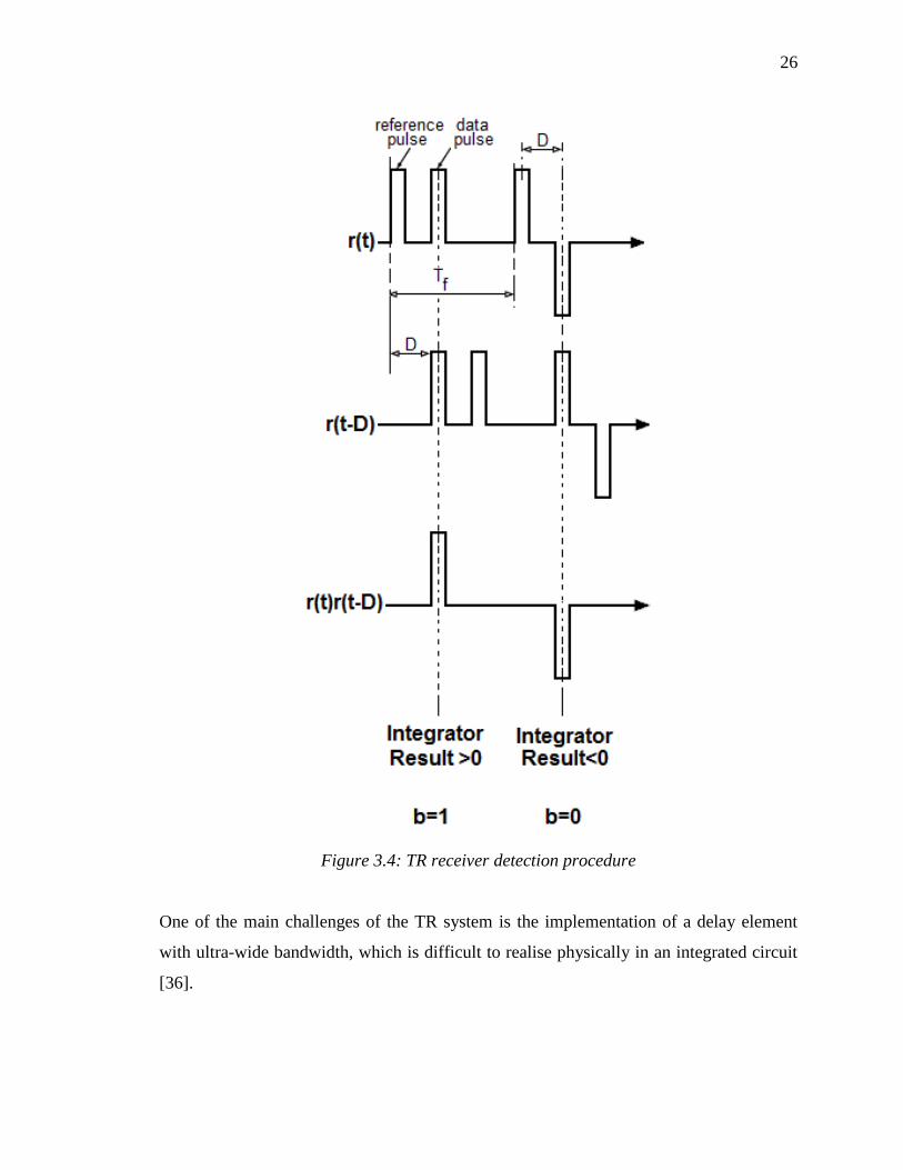
Figure 3.3: General TR receiver structure [36]
The general structure of the TR receiver is illustrated in Figure 3.3. The received signal is
delayed by the known delay element, D. In this way the reference pulse is used as a
template to extract the data pulse. Figure 3.4 shows the detection procedures of the TR
receiver.
26
Figure 3.4: TR receiver detection procedure
One of the main challenges of the TR system is the implementation of a delay element
with ultra-wide bandwidth, which is difficult to realise physically in an integrated circuit
[36].
27
3.1.3 Frequency Shifted Reference
Another scheme that has arisen for UWB transmission is Frequency-Shifted Reference
(FSR), which aims to separate the data pulse and reference pulse in the frequency domain
rather than the time domain. The motivation behind FSR is that implementation of a
frequency shift for a wideband signal is simpler to achieve than the implementation of a
wideband delay for the same signal [36]. We recall from the TR method that in order to
effectively use the reference pulse as a template for the data pulse, both pulses must
undergo the same channel distortion and fading; i.e. the delay time between the two
pulses must be significantly less than the coherence time of the channel. For the FSR
scheme this constraint becomes that the frequency offset (f0) between the reference and
data pulse must be much smaller than the coherent bandwidth of the channel [36].
In [36], the method of Slightly Frequency-Shifted-Reference Receiver is suggested to
satisfy the above constrain. To explain this method, transmission can be considered to be
in the terms of frames and symbols:
(3.1)
where Ts is the time period per symbol, Nf is the number of frames where there is one
pulse per frame, and Tf is the time period per frame. A reference pulse sequence and one
or more data pulse sequences are simultaneously transmitted; where each data pulse
sequence is shifted by a specific frequency offset [36].
In order to ensure orthogonality between the reference pulse sequence and the data pulse
sequences, the orthogonality is ensured over each symbol period, rather than by frame
period, therefore [36]:
sff
offsetTTN
f11
(3.2)
The general structure of the FSR receiver when only one data sequence is transmitted is
shown in Figure 3.5. The frequency offset, fo, is the same offset that was used to shift the
data sequences before transmission. On the receiver side this offset will shift the
28
reference pulse sequence so that it may be used as a template to extract the information
from the data pulse sequences.
Figure 3.5: General FSR receiver structure [36]
Due to the analog frequency offsets employed in the FSR scheme, the performance of the
system can be affected by frequency errors caused by oscillator mismatch, phase errors
caused by multipath fading, and amplitude errors caused by nonlinear amplifiers [1].
Therefore the reference pulse sequence may not provide a perfect template for the data
pulse sequence.
3.2 CODE-SHIFTED REFERENCE (CSR)
Recently proposed is that of the Code-Shifted Reference (CSR) scheme for the IR-UWB
Receiver. In the CSR scheme, rather than being separated by time (TR) or by frequency
(FSR), the reference and data pulse sequences are separated by codes [1].
29
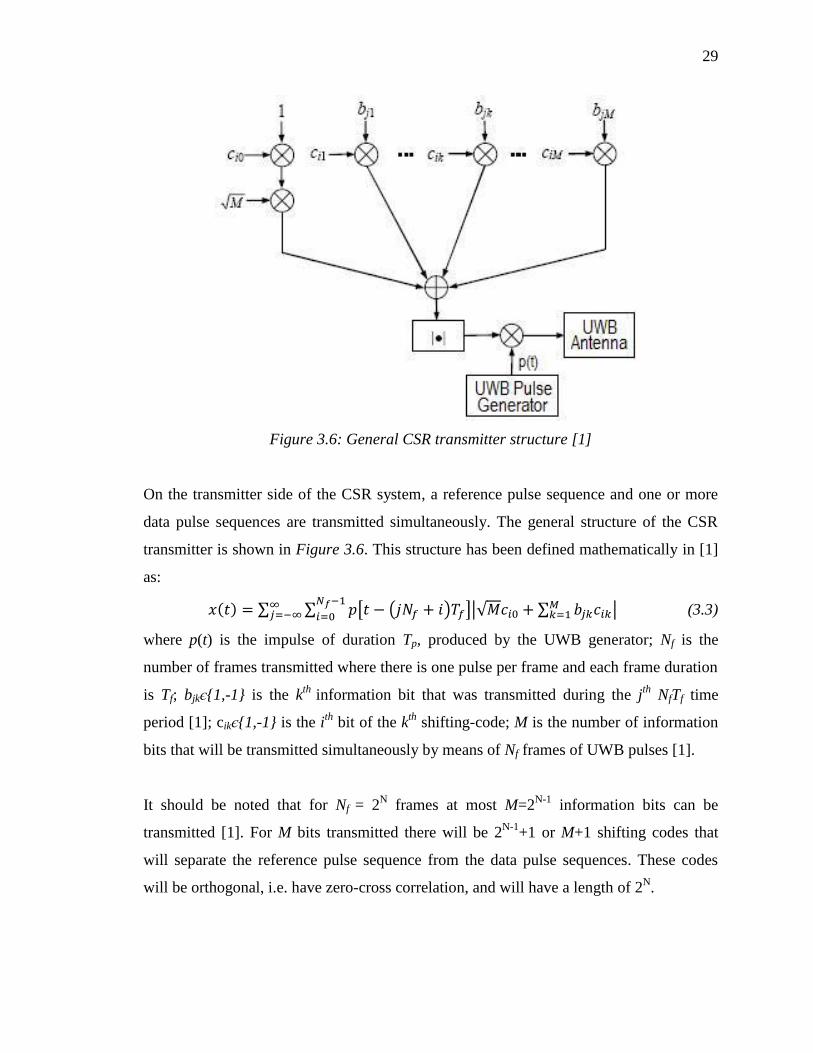
Figure 3.6: General CSR transmitter structure [1]
On the transmitter side of the CSR system, a reference pulse sequence and one or more
data pulse sequences are transmitted simultaneously. The general structure of the CSR
transmitter is shown in Figure 3.6. This structure has been defined mathematically in [1]
as:
(3.3)
where p(t) is the impulse of duration Tp, produced by the UWB generator; Nf is the
number of frames transmitted where there is one pulse per frame and each frame duration
is Tf; bjkє{1,-1} is the kth
information bit that was transmitted during the jth
NfTf time
period [1]; cikє{1,-1} is the ith
bit of the kth
shifting-code; M is the number of information
bits that will be transmitted simultaneously by means of Nf frames of UWB pulses [1].
It should be noted that for Nf = 2N frames at most M=2
N-1 information bits can be
transmitted [1]. For M bits transmitted there will be 2N-1
+1 or M+1 shifting codes that
will separate the reference pulse sequence from the data pulse sequences. These codes
will be orthogonal, i.e. have zero-cross correlation, and will have a length of 2N.
30
On the receiver side of the CSR systems, M (=2N-1
) orthogonal detecting codes of length
2N are used to extract the information from the data sequence. The general structure of
the CSR receiver is illustrated in Figure 3.7.
Figure 3.7: General CSR receiver structure [1]
Referring to Figure 3.7, filtering is performed to remove any noise and interference
beyond the desired signal band, followed by a square unit and then integrated from
(jNf+i)Tf to (jNf+i)Tf+TM to obtain rij. The value of TM varies from Tp in an additive white
Gaussian noise (AWGN) channel to Tf in a multipath channel with severe delay spread
[1]. Although a larger value of TM, will result in the collection of more signal energy
distributed in different MPCs, this also results in added noise and interference. [1]
The signal, rij, is correlated with the M detection codes and then each result is summed
independently. The sign of the results of these summations will determine whether the
received information bits will be detected as logic „1‟ or „0‟, defined in [1] as:
(3.4)
31
3.2.1 Differential Code-Shifted Reference (DCSR)
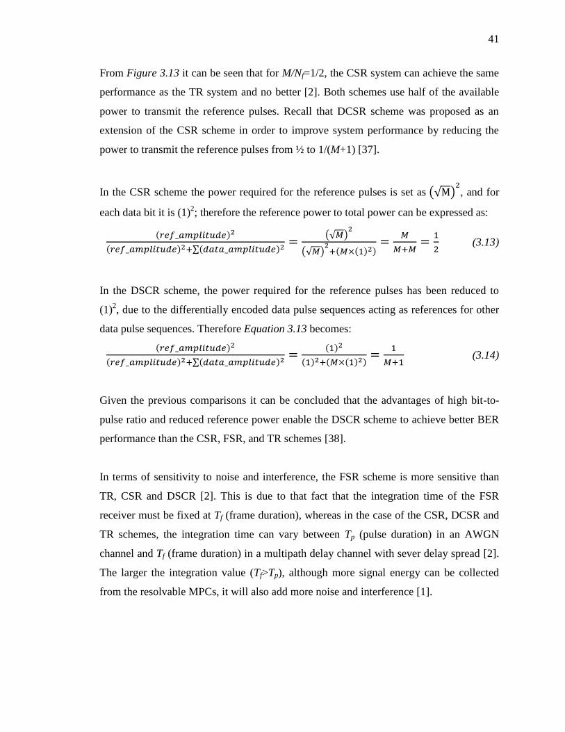
The CSR scheme is able to eliminate some of the issues regarding the complexity of the
TR scheme and the performance degradation of the FSR scheme. But the CSR system,
like the TR system, spends half of its power transmitting the reference pulse sequence
[2]. Therefore the CSR system, although having reduced implementation complexity
when compared to the TR system, cannot achieve better BER performance than the TR
system. In order to improve system performance, the CSR scheme was extended to the
differential CSR (DSCR) as presented in [37]. This performance improvement is
achieved by reducing the amount of power used to transmit the reference pulse sequence
[37].
The DSCR method makes use of the fact that the CSR scheme can transmit multiple data
pulse sequences simultaneously, where each data pulse sequence bears one information
bit. In the DCSR scheme, the information bits are differentially encoded so that one data
pulse sequence can be used as a reference for another data pulse sequence. Therefore,
when M bits are transmitted simultaneously, the amount of power used to transmit the
reference pulse sequence can be reduced from ½ to 1/(M+1). [37]
Figure 3.8: General DCSR transmitter structure [37]
32
The general structure of the DCSR transmitter is shown in Figure 3.8. This structure has
been defined mathematically in [37] as:
(3.5)
where p(t) is the impulse of duration Tp, produced by the UWB generator; Nf is the
number of frames transmitted where there is one pulse per frame and each frame duration
is Tf; cikє{1,-1} is the ith
bit of the kth
shifting-code; M is the number of bits that will be
transmitted simultaneously by means of Nf frames of UWB pulses [37]; djk is the kth
differentially encoded information bit that was transmitted during the jth
NfTf time period,
defined in [37] as:
(3.6)
where bjlє{1,-1} is the lth
information bit that was transmitted during the jth
NfTf time
period [37].
For DCSR, the number of information bits that can be transmitted in Nf(=2N) frames is
determined by M(M+1)/2≤2N-1. For example, given: Nf=4, M=2; Nf=8, M=3; Nf=16,
M=5. For M bits transmitted there will be M+1 orthogonal shifting codes that will
separate the reference bit from the data bits, where the length of each code equal to Nf.
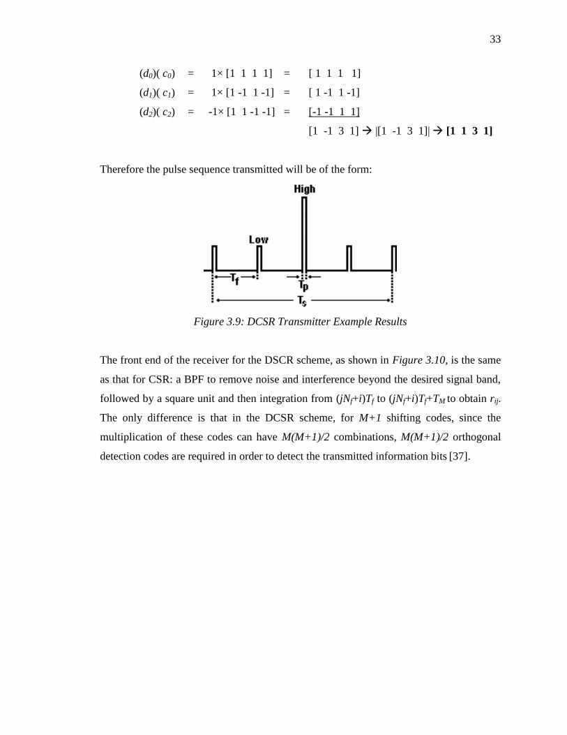
Take the following example:
Number of frames = Nf = 4,
Number of Bits = M = 2,
Number of shifting codes required = (M+1) = 3, Code length = 4
Bits to transmit: b1=1, b2=-1
dj0 = 1
dj1= bj1 = 1
dj2= (bj1)(bj2) = (1)(-1) = -1
Orthogonal shifting codes: c0=[1 1 1 1], c1=[1 -1 1 -1], c2=[1 1 -1 -1]
33
(d0)( c0) = 1× [1 1 1 1] = [ 1 1 1 1]
(d1)( c1) = 1× [1 -1 1 -1] = [ 1 -1 1 -1]
(d2)( c2) = -1× [1 1 -1 -1] = [-1 -1 1 1]
[1 -1 3 1] |[1 -1 3 1]| [1 1 3 1]
Therefore the pulse sequence transmitted will be of the form:
Figure 3.9: DCSR Transmitter Example Results
The front end of the receiver for the DSCR scheme, as shown in Figure 3.10, is the same
as that for CSR: a BPF to remove noise and interference beyond the desired signal band,
followed by a square unit and then integration from (jNf+i)Tf to (jNf+i)Tf+TM to obtain rij.
The only difference is that in the DCSR scheme, for M+1 shifting codes, since the
multiplication of these codes can have M(M+1)/2 combinations, M(M+1)/2 orthogonal
detection codes are required in order to detect the transmitted information bits [37].
34
Figure 3.10: General DCSR receiver structure [37]
Continuing with the example used to explain the DCSR transmitter, for the information
detection block of Figure 3.10:
rij=[1 1 9 1] (squared amplitudes of transmitted signal)
Number of shifting codes required = M(M+1)/2= 3, Code length = 4
Orthogonal detection codes: c01=[1 -1 1 -1], c02=[1 1 -1 -1], c12=[1 -1 -1 1]
(rij)(c01) = [1 1 9 1] × [1 -1 1 -1] = [1 -1 9 -1]
(rij)(c02) = [1 1 9 1] × [1 1 -1 -1] = [1 1 -9 -1]
(rij)(c12) = [1 1 9 1] × [1 -1 -1 1] = [1 -1 -9 1]
∑(rij)(c01) = r01 = +8
∑(rij)(c02) = r02 = -8
∑ (rij)(c12) = r12 = -8
The information bits are determined by means of the following decision rule for
joint detection [37]:
(3.7)
35
Given M=2 and for j=1,
To find , means to find the value of bit bk,
that will result in the maximum for the previously calculated summations, rln. In
this example the maximum will be +8.
r01 = +8 r01b1 = 8 b1 = 1
r02 = -8 r02b1 b2 = 8 b1 b2 = -1
r12 = -8 r12b2 = 8 b2 = -1
3.3 PERFORMANCE COMPARISON
The CSR scheme offers advantages over the TR and FSR schemes. Since the data pulses
and reference pulse are shifted by means on code rather than time, a wideband delay
element is not required; therefore system complexity is reduced when compared with the
TR system. Also since digital codes are employed rather than analog carriers to provide
the separation between the reference and data pulse sequences, the CSR scheme is able to
avoid most of the performance degradation that occurs in the FSR scheme due to errors in
frequency, amplitude and phase. [1]
A theoretical analysis of the performance of the CSR scheme compared to other schemes
was recently presented in [2]. Also performance comparison between the DCSR and the
CSR/TR/FSR schemes was presented in [38]. It should be noted that in these papers
comparison on the performance of the systems was made assuming that no inter-pulse
interference existed.
36
The bit error rate (BER) of the CSR receiver in a multipath environment was found as
[2]:
(3.8)
where Eb is the received energy per information bit, No is the single-side power spectral
density of AWGN, M is the number of information bits transmitted, (fh―fl) is the
bandwidth of the UWB signal, Nf is the number of frames transmitted, Tm is a time value
used in receiver integration (varies from the value of pulse duration, Tp, in an AWGN
channel to the value of frame duration, Tf, in a multipath channel with severe delay
spread [1]), and α is a constant value ranging from (0,1] according to Tm (α=0 for Tm=0
and α=1 for TM=Tf) [38].
Computer simulation for the BERs of the CSR system as a function of Eb/No was
performed in order to verify the theoretically calculated results [2]. These results
illustrated in Figure 3.11 were simulated under the conditions that Tf=60ns to ensure that
inter-pulse interference would not exist, and TM=Tf so that α is fixed at 1 [38].
Figure 3.11: BER of the CSR system: theoretical vs. simulation results [2]
37
From Figure 3.11 it can be seen that the simulated results match closely with what are
predicted by the theoretically analysis. Also for a fixed number of frames (one pulse per
frame) and fixed frame duration, it was found that the BER of the CSR system improved
as more information bits were transmitted simultaneously, i.e. for larger values of M.
The BER of the DCSR receiver in a multipath environment was found as being bounded
by [38]:
(3.9)
(3.10)
In the same way, computer simulation of the DCSR BER as a function of Eb/No was
performed [38]. The results illustrated in Figure 3.12 were also simulated under the
conditions that Tf=60ns to ensure that inter-pulse interference would not exist, and TM=Tf
so that α is fixed at 1 [38].
38
Figure 3.12: BER of the DCSR system: theoretical vs. simulation results [38]
As was the case with CSR, it can be seen that for a fixed number of frames of fixed
duration, as the number of bits transmitted simultaneously increases the performance of
the DCSR system improves. This Figure also shows that if the frame to bit ratio is
reduced, (4:2 as opposed to 8:2) the performance is also improved.
For the performance comparison of the DSCR and CSR systems with the FSR and TR
systems, [2] provided the following equations for the BER of the FSR system (under
AWGN environment) and the TR system (under multipath environment):
(3.11)
(3.12)
39
Using these equations and the BER equations derived for DCSR and CSR, comparison
was made between the systems for instances where M=2 and M=3 as shown in Figure
3.13 and Figure 3.14 respectively.
Figure 3.13: BER comparison between DCSR, CSR, FSR and TR, M=2 [38]
40
Figure 3.14: BER comparison between DCSR, CSR, FSR and TR, M=3 [38]
Referring to the cases presented in these Figures, the FSR system has the worst
performance, while the DCSR system has the best performance. For the FSR system, the
number of bits that can be transmitted simultaneously is limited by the number of analog
carriers available [2]. For Nf=6, as shown in Figure 3.13, there are only two analog
carriers available, and M can only be „1‟ or „2‟ [2]. Therefore the highest achievable bit-
to-pulse ratio (M/Nf) for the FSR system when Nf=6 is 1/3 (or 2/6) [38]. Comparing this
result to the other systems shown in Figure 3.13, their highest achievable bit-to-pulse
ratio is M/Nf=½ (or 2/4). When M=3, the FSR system requires Nf=10, while the TR
system requires Nf=6. In general the FSR system will achieve a bit-to-pulse ratio of less
than ½, while the TR system will achieve a bit-to-pulse ratio equal to ½. For the CSR and
DSCR systems, the bit-to-pulse ratio can be up to ½ and has the flexibility to transmit
less than ½ as shown in Figure 3.14 where 3 bits are transmitted simultaneously within 8
frames, although a max of 4 bits could have been transmitted with 8 frames.
41
From Figure 3.13 it can be seen that for M/Nf=1/2, the CSR system can achieve the same
performance as the TR system and no better [2]. Both schemes use half of the available
power to transmit the reference pulses. Recall that DCSR scheme was proposed as an
extension of the CSR scheme in order to improve system performance by reducing the
power to transmit the reference pulses from ½ to 1/(M+1) [37].
In the CSR scheme the power required for the reference pulses is set as , and for
each data bit it is (1)2; therefore the reference power to total power can be expressed as:
(3.13)
In the DSCR scheme, the power required for the reference pulses has been reduced to
(1)2, due to the differentially encoded data pulse sequences acting as references for other
data pulse sequences. Therefore Equation 3.13 becomes:
(3.14)
Given the previous comparisons it can be concluded that the advantages of high bit-to-
pulse ratio and reduced reference power enable the DSCR scheme to achieve better BER
performance than the CSR, FSR, and TR schemes [38].
In terms of sensitivity to noise and interference, the FSR scheme is more sensitive than
TR, CSR and DSCR [2]. This is due to that fact that the integration time of the FSR
receiver must be fixed at Tf (frame duration), whereas in the case of the CSR, DCSR and
TR schemes, the integration time can vary between Tp (pulse duration) in an AWGN
channel and Tf (frame duration) in a multipath delay channel with sever delay spread [2].
The larger the integration value (Tf>Tp), although more signal energy can be collected
from the resolvable MPCs, it will also add more noise and interference [1].
42
Another issue for comparison is that of peak-to-average-power-ratio (PAPR):
(3.15)
Independent of the number of bits transmitted (M), the TR scheme is able to achieve
PAPR=0dB, given that all the pulses have the same amplitude:
(3.16)
According to [38] the dB equations for the PAPR for the FSR, CSR and DSCR schemes
can be defined as follows:
(3.17)
(3.18)
(3.19)
Therefore for a fixed value of M, the FSR scheme has the highest PAPR, the TR scheme
has the lowest PAPR, while the DSCR and CSR schemes have a medium PAPR. [38]
43
CHAPTER 4: FIRST PROPOSED CSR
TRANSMITTER
The circuit described in this Chapter is based on the design of the first attempt of the CSR
transmitter. The theoretical and simulation results of this transmitter were first given in
[3] (written by thesis author). It was found after implementation and testing that this
design was not able to effectively achieve the theorized results. Therefore the transmitter
was modified to overcome the problems that were faced. In this Chapter, the design
theory of each block of the original transmitter design is presented as well as the
simulation and implementation results. These results are presented to offer a comparison
of this transmitter with the second transmitter design (the final design for the proposed
transmitter). The design and results of the modified transmitter are presented in Chapter
5.
4.1 DESIGN THEORY
Figure 4.1: Block diagram of first design of CSR Transmitter
44
The general structure of the first design of the CSR transmitter is illustrated in Figure 4.1.
The transmitter consists of three stages. The first stage is that of impulse generation; the
second stage is the gated pulse stage, which gates an input radio frequency with the
previously generated impulse; and the final stage is an amplitude modulation stage used
to vary the amplitude of the impulses based on the control codes provided by an FPGA.
The aim of this transmitter is to generate the required CSR signals while providing
flexibility and independence among the generated pulse width, center frequency, and
pulse repetition rate.
4.1.1 Stage1: Pulse Generation
For a UWB system, the pulse generator serves as one of the most challenging units in
terms of design. This unit is also considered one of the most critical due to the fact that
the nature of the generated impulses, i.e. its shape and duration, determine the bandwidth
and spectral shape of the transmitted signal. In other words, the pulse generator will
determine whether the transmitted signal will comply with the FCC spectral limits.
Since the authorization for the unlicensed commercial use of UWB technologies by the
FCC in 2002, research effort worldwide has been made to develop UWB transmitters that
provide a good balance between complexity and power consumption, and a suitable pulse
shape that will make the best use of the FCC spectral mask. In terms of the UWB pulse
generator, several different types of circuit implementations have been proposed in
literature. For instance, pulse generators have been proposed based on step-recovery-
diodes (SRD), and microstrip lines [41], which are easy to fabricate at the board level and
provide a good trade-off between pulse performance and current consumption [41].
However, the rise-time of the pulse is limited by the diode due to biasing conditions and
parasitic due to diode packaging [39]. Several “all digital” generators implemented in
CMOS have been proposed, which provide “flexibility in terms of programmability”
[43], but CMOS technology has difficulty in operating at the high frequencies [42], which
leads to high complexity for CMOS to operate at very high clock speeds required for fast
45
data rates [43]. Furthermore, there is difficulty in realizing digital filters for UWB pulses
with CMOS technology [43]. Also proposed have been impulse generators based on
avalanche transistors, which provide “very fast and potentially high amplitude pulses”
[44], but are limited by the pulse repetition frequency [44].
For this research work, the circuit proposed and implemented for the „Pulse Generator‟
stage is illustrated in Figure 4.2. This pulse generator consists of a delay element and
several high speed transistors which are used to provide „logic gate‟ functions.
Figure 4.2: Transmitter ‘Pulse Generation’ stage
4.1.1.1 FPGA input and Buffer
The input „Clk‟ to the impulse generator circuit is a clock signal generated digitally by an
FPGA board. The clock controls the pulse repetition rate for the UWB transmit signal.
The input signal is first buffered in order to regulate any input resistance to the circuit.
The buffer is implemented by means of a voltage follower as shown in Figure 4.2.
Therefore the signal output „A‟ will „follow‟ the signal input with its amplitude reduced
by a 0.7V (VBE) voltage drop.
46
4.1.1.2 Delay
The buffered clock signal is then delayed by means of an RC (resistor-capacitor) circuit.
The value of the delay is determined by the values of the resistor and capacitor such that
(4.1)
This delay will determine the width of the generated pulse. In turn, the width of the UWB
pulse determines the spectral bandwidth of the signal.
4.1.1.3 Inverter and NOR gate
Both the inverter and NOR gate are implemented by means of Resistor-Transistor Logic.
Referring to Figure 4.2, the NOR gate acts to combine the buffered signal produced at
„A‟ with the delayed-inversion of the signal that results at „C‟. The function of the NOR
gate is to produce a „high‟ output only when both „A‟ and „C‟ are „low‟. At all other
instances the NOR gate will output a „low‟ signal.
Figure 4.3: Theoretical time domain pulse waveforms for impulse generator
Figure 4.3 shows the theoretically expected waveforms at each stage of the „Pulse
Generator‟. The circuit is expected to produce an impulse of duration τ on every falling
clock edge. The rate at which the impulses are produced is dependent on the clock signals
provided by the FPGA, such that the pulse repetition rate (PRR) is given by:
(4.2)
47
4.1.2 Stage 2: Pulse Gating
The purpose of this stage is to control the center frequency of the signal spectrum such
that it will lie in the frequency bandwidth available for UWB transmission. The concept
of pulse gating can be best explained by means of Figure 4.4. In this circuit the
bandwidth of the spectrum is controlled by the „opening‟ and „closing‟ of the switch (i.e.
the duration of the pulse that the switch generates), while the center frequency of the
spectrum is determined by the radio frequency (RF) inputted to the switch. The duration
for which the gate is „open‟ controls the duration of the frequency signal allowed though,
therefore it can be said that the frequency has been „gated‟ by the switch.
Figure 4.4: Concept of Pulse Gating in the time domain
This concept has been implemented in the transmitter by means of the circuit illustrated
in Figure 4.5. In this circuit a BJT has taken the place of the switch in Figure 4.4 and
performs the same function.
Figure 4.5: Transmitter ‘Gated Pulse’ stage
48
When no voltage (0V) is applied to the base (b) of the BJT it will be operating in the cut-
off region, therefore current at both collector (c) and base (b) terminals will be ideally
zero. When operating in the cut-off region the BJT is not conducting and appears as an
„open circuit‟ or „open switch‟ between the collector (c) and emitter (e) terminals. As a
result, no signal will be observed at „E‟.
When a sufficient amount of voltage is applied to the base (b) of the BJT it will operate in
the saturation region. In this region the BJT is fully conducting and acts as a „short
circuit‟ or „closed switch‟ between the collector (c) and emitter (e) terminals. As a result,
the RF signals passes from collector (c) to „E‟. The duration for which the BJT is „closed‟
is dependant of the width, τ, of the impulse generated previously and shown as waveform
„D‟ in Figure 4.3.
In order to control the flow of AC from „Freq‟ to „E‟, and of DC from „Vin‟ to ground,
blocking capacitors and inductors have been used. The capacitors in the circuit act as DC
blocking capacitors, allowing the high frequency „Freq‟ to pass freely while blocking the
DC signal „Vin‟. The inductors act as AC blocking, allowing the DC to pass while
providing high impedance to the high frequency.
Figure 4.6: Theoretical time domain response of the ‘Gated Pulse’ stage
49
The output at „E‟ is expected to resemble the pulse shown in Figure 4.6. Note that the
output will have no DC component due to the DC blocking.
4.1.3 Stage 3: Signal Coding
As was mentioned in Section 3.2, digital shifting-codes will be used to encode the data
and reference pulse sequences. The encoding of the bits according to the appropriate CSR
algorithm, be it traditional CSR or the modified DSCR method, is performed by the
coding supplied to the FPGA of the system. The result will be a pulse sequence of varied
amplitudes corresponding to the results of the encoding. For instance, it was shown in the
example of Section 3.2, that the DSCR encoding of bits b1=1 and b2=-1 resulted in a
sequence of [1 1 3 1]. Based on the resulting pulse sequence, the FPGA will provide
control signals to the VGA indicating which pulses should be amplified and which should
remain un-amplified to correspond to encoded results. This occurrence is illustrated in
Figure 4.7.
Figure 4.7: Concept of pulse coding by the VGA
50
4.2 SIMULATION RESULTS
In order to determine the performance of the proposed transmitter, simulation of the first
two stages, „Pulse Generator‟ and „Gated Pulse‟ was conducted with Agilent‟s Advanced
Design System (ADS). The schematic of the circuit simulated in ADS is illustrated in
Figure 4.8.
For simulation of the system, it was chosen to use an input clock signal of 20MHz and a
spectrum centered at 4.44GHz. It should be noted that transmission is in lower half of the
UWB spectrum (3-5GHz). This is to avoid any interference that may occur with WLAN
systems operating at 5GHz. The duration of the generated pulse was chosen to be 4ns. It
should be noted that given this width, the pulse will not be considered a UWB pulse until
it has undergone pulse gating. The 4ns pulse on its own will only have a bandwidth of
250MHz. After pulse gating the spectra of this pulse will have 250MHz above 4.44GHz
and 250MHz below 4.44GHz, therefore achieving the minimum 500MHz bandwidth for
it to be considered a UWB signal.
Figure 4.9 shows the simulated results corresponding to the points „A‟, „B‟, „C’ and „D‟
of the „Pulse Generator‟ of Figure 4.2. „A‟ is the output after the buffer. „B‟ is the
delayed signal and „C’ is the inversion of this signal. „D‟ shows the results after the
buffered signal at „A‟ has been NOR-ed with the inverted signal at „C’. The „Pulse‟
waveform of Figure 4.9 illustrates that the simulated circuit of Figure 4.8 is able to
produce a pulse sequence at a pulse repetition rate of 50ns (20MHz), where each impulse
has a 4ns pulse width.
51
Figure 4.8: Simulation schematic of ‘Pulse Generation’ and ‘Gated Pulse’ stages
52
1
2
0
3
Clk
_in
, V
1
2
0
3B
uff
ere
d,
V
0.5
1.0
0.0
1.5
De
laye
d,
V
1
2
3
0
4
Inve
rte
d,
V
20 40 60 800 100
1
2
3
0
4
time, nsec
Pu
lse
, V
26.00n209.1m
m2
29.71n187.0m
m3
m2time=Pulse=186.8mV
25.80nsec
m3time=Pulse=187.0mV
29.71nsec
Figure 4.9: Simulation results of ‘Pulse Generation’ stage
A
B
C
D
53
Figure 4.10 shows the results after the „Gated Pulse‟ stage. From Figure 4.10a it is clear
that the input frequency is effectively gated by the 4ns pulse generated prior. Figure
4.10b is an expansion of one of the gated pulses. Markers „m4‟ and „m5‟ show that 4ns of
the input frequency have been gated. Marker „m6‟ and „m7‟ illustrate that the period
between cycles is approximately 0.22ns (≈1/4.44GHz). Therefore we have obtained the
4.44GHz frequency gated within the 4ns pulse.
m4time=Gated=2.737mV
26.00nsec
m5time=Gated=2.536mV
30.00nsec
20 40 60 800 100
-2
-1
0
1
2
-3
3
time, nsec
Ga
ted
, V
Readout
m4
Readout
m5
m4time=Gated=2.737mV
26.00nsec
m5time=Gated=2.536mV
30.00nsec
(a)
m4time=Gated=6.197mV
26.10nsec
m5time=Gated=6.915mV
30.06nsec
m6time=Gated=1.913
27.50nsec
m7time=Gated=1.989
27.72nsec
22 24 26 28 30 32 3420 36
-2
-1
0
1
2
-3
3
time, nsec
Ga
ted
, V
Readout
m4
Readout
m5
Readout
m6
Readout
m7
m4time=Gated=6.197mV
26.10nsec
m5time=Gated=6.915mV
30.06nsec
m6time=Gated=1.913
27.50nsec
m7time=Gated=1.989
27.72nsec
(b)
Figure 4.10: Simulation results of the (a) ‘Gated Pulse’ stage and (b) Magnification of
the gated pulse
54
Figure 4.11 shows the spectral response of the final pulse produced by the simulated
system. It can be seen that the pulse does indeed conform to the FCC spectral mask. It
should be noted that the mask has been shifted upwards to match the maximum value of
the spectral response. Therefore the spectrum will have to be shifted after pulse
generation to meet the -41.3dBm limit. It Figure 4.11 also illustrates that the spectral
response of the pulse does not make the best use of the UWB spectral mask. But at
present we are unconcerned with the shape of the pulse (i.e. how it occupies the
spectrum). We are simply trying to implement the UWB CSR scheme in a real system.
Methods for making better use of the spectrum are considered future work and options
for achieving this will be discussed in the final Chapter of this thesis.
Figure 4.11: Spectral response of the simulated pulse results against FCC indoor mask
55
4.3 IMPLEMENTATION RESULTS
The circuit boards were implemented using FR4 double-sided copper-clad boards. The
printed circuit board (PCB) layout was accomplished using ADS and a copy of the layout
of the transmitter has been included in the Appendix for reference. The schematic
corresponding to the full implemented transmitter system is illustrated in Figure 4.12. To
reduce the cost of implementing the system, the components used were chosen to be off-
the-shelf surface-mount (SMT) components. The values of the discrete components and
labels for the integrated circuit (IC) components have been included in schematic of
Figure 4.12. This Figure also illustrates all bias values and input signal values to the
circuit.
Testing of the board was accomplished with the use of the Agilent Infiniium 54831D
MSO oscilloscope. This is a 4-probe oscilloscope with a bandwidth of 600MHz and
sampling rate of 4GSa/sec. Due to the bandwidth limitations of the oscilloscope the
transmitter was tested with a 400MHz input frequency so that the results could be
properly viewed. Although this will not place the spectrum of the signal in the UWB
transmission band, as would have been the case if an input frequency of 4.44GHz was
used, it is sufficient to test the functionality of the transmitter.
56
Figure 4.12: Full Schematic of the first Transmitter design
57
Figure 4.13 gives the results of the „Pulse Generator‟ portion of the circuit. The first
waveform is that of the 20MHz input clock supplied by the FPGA. The second waveform
is the signal after it has passed through the buffer circuit. It can be seen that the buffer
produced the expected results of a signal that followed the clock signal and whose
amplitude was reduce by approximately 0.7V. The third waveform is the signal result
after it had passed through both the delay and inverter portions of the circuit. The final
waveform is that of the impulse produced by the pulse generator. It can be seen that this
pulse was effectively generated when both the buffer signal and the inverted delay signal
were low, achieving the pulse repetition rate of 50ns (20MHz).
Figure 4.13: Implementation results after ‘Pulse Generation’
Figure 4.14 illustrates the resulting waveform after the signal has passed through the
„Gated Pulse‟ stage. Recall that here a 400MHz frequency was supplied to be gated as
opposed to the desired 4.44GHz due to the bandwidth limitations of the oscilloscope.
From this Figure it can be seen that the input frequency was not gated as efficiently as
desired. There is quite a bit of the frequency signal leaking through between impulses
when the signal is expected to be low. This leakage is quite high in comparison to the
58
amplitude of the pulse. Also from this Figure it can be seen that the 50ns pulse repetition
rate has been maintained.
Figure 4.14: Implementation results after ‘Pulse Gating’
Figure 4.15 shows the signal results at output of the transmitter. Note that the signal
illustrated in this Figure is measured directly at the output of the VGA, before
transmission to the antenna, and is not the signal result as transmitted through the air. The
aim of the VGA was to provide a variation in the amplitude between „high‟ and „low‟
pulses depending on the control signal received from the FPGA. The result of whether a
„high‟ or „low‟ amplitude was applied to the pulse was dependent of the results of
encoding performed by the FPGA. Differential CSR was used as the encoding method
within the FPGA. For the testing of the system, a random M-bit sequence was generated,
where simultaneous transmission was for 2 bits to be sent in 4 frames. After encoding the
bit steam, the control from the FPGA was expected to yield the results of the form:
[1 1 1 3] [3 1 1 1] [1 1 3 1] [1 3 1 1] [1 1 3 1] [1 1 1 3]
[1 1 3 1] [3 1 1 1] [3 1 1 1] [1 1 3 1] [1 1 1 3] [1 3 1 1]
[3 1 1 1] [1 1 1 3]
Note that the above sequences to be applied to the generated pulse sequence do not
indicate that the results will have the exact amplitudes of 3Volts and 1Volt. Only the ratio
between the „high‟ and „low‟ pulse will 3:1, therefore „high‟=x3 and „low‟=x1.
Figure 4.15: Implementation results after VGA
59
From the results of Figure 4.15 it can be seen that after the VGA output it is difficult to
distinguish between pulses. The pulse duration seems to have been spread and the pulses
merge into one another. It was assumed that the reason for this may be due to the settling
time of the VGA. The settling time is time it will take for the VGA to make a complete
transition between one amplitude-value to another. If the settling time is longer than the
pulse repetition rate the VGA will not have enough time to reach the desired amplitude.
Also if the switching speed of the latch was slow it may have also caused these undesired
results. When the latch is set the gain value produced by the VGA will remain constant.
Therefore if the switch speed time was much greater than the pulse width, this could
result in some of the noise that existed outside of the 4ns pulse being amplified as well.
Given the results after the „Gated Pulse‟ stage there was a significant amount of the
frequency signal that leaked through when the gate was supposed to be open, i.e. have no
signal passing through. This leakage may have been amplified as well if the switching
speed was slow.
In order to confirm if the settling time of the VGA had any impact on the final results, the
clock rate applied to the transmitter was reduced, i.e. the pulse repetition rate was
decreased. The clock was first reduced to 5MHz, the results of the transmitter with this
clock speed are illustrated in Figure 4.16a. The clock was then further reduced to a value
of a 100KHz, yielding the results of Figure 4.16b. From these Figures it can be seen that
as the clock rate was reduced, it was easier to distinguish between the „high‟ and „low‟
pulses.
60
(a)
(b)
Figure 4.16: Implementation results after VGA with clock rate of (a) 5MHz and
(b)100KHz
4.4 CONCLUSIONS
Overall the transmitter was unable to achieve the results that were expected. The „Pulse
Generator‟ of the transmitter was able to efficiently provide an impulse of 4ns. The pulse
gating by means of the BJT switch did not perform as precisely as expected. A small
amount of the input frequency leaked through when the switch was supposed to be „open‟
and have no signal appear at the output. The major problem faced by the transmitter was
in the performance provided by the VGA. It was found that the speed of the VGA was
not fast enough to accommodate the required clock speed, therefore limiting the data-rate
of the system. This would be even more problematic if we desired higher clock rates. The
61
idea of using a VGA to vary the amplitudes was abandoned due to the fact that this was
the only SMT VGA that could be found at the time which was able to satisfy the
necessary bandwidth requirements of the system. Therefore alternate methods for
performing the gating function and amplitude modulation were considered, and are
presented in the revised transmitter design of Chapter 5.
62
CHAPTER 5: PROPOSED CSR TRANSMITTER
Due to the fact that the speed of the VGA was not fast enough to accommodate the
required clock speed, as described in the previous Chapter, the first transmitter designed
was not able to accomplish what was theoretically expected. It was then modified and
redesigned as the transmitter elaborated in the following Sections.
5.1 DESIGN THEORY
Figure 5.1: Block Diagram of CSR Transmitter
The general structure of the proposed CSR transmitter is illustrated in Figure 5.1. The
transmitter consists of three stages. The first stage is that of „Pulse Generation‟ consisting
of two identical impulse generators; the second is an „Amplitude Modulation‟ stage used
to encode the impulses via amplitude; and the final stage is the „Gated Pulse‟ stage which
gates an input radio frequency with the generated impulse.
63
5.1.1 Stage1: Pulse Generator
The circuit implementation of „Pulse Generator 1’ and „Pulse Generator 2‟ are basically
identical to the pulse generator that was presented in the first design of the transmitter
(see Figure 4.2 of Chapter 4). The only difference between the two is that the AC
blocking inductors included in the pulse generator of the previous design (Figure 4.2)
have been removed. Instead, decoupling capacitors have been placed between the trace
paths connected to the voltage supply and ground to reduce any noise to the circuit, i.e.
any noise from the voltage source will be redirected through the capacitors to ground
while DC will pass through to the circuit. The circuit implementation of the revised
„Pulse Generator‟ stage is illustrated in Figure 5.2. It should be noted that the only
difference between the two generators shown in Figure 5.2 is in the clock signal that each
generator receives from the FPGA.
Figure 5.2: Revised transmitter ‘Pulse Generation’ stage
64
The function of these two generators is exactly the same as the one presented in Chapter
4, therefore the details of each section of the „Pulse Generator‟, i.e. „Buffer‟, „Delay‟,
„Inverter‟ and „NOR Gate‟, will not be reiterated here.
5.1.2 Stage2: Amplitude Modulation
The circuit illustrated in Figure 5.3 codes the impulses provided by the two generators by
means of amplitude modulation and then combines the two signals into a single pulse
sequence for transmission.
Figure 5.3: Revised transmitter ‘Amplitude Modulation’ stage
Both amplitude modulation branches use an operational amplifier (op-amp) in order to
alter the amplitudes of the incoming pulse sequences. The structure of these amplifiers is
referred to as an „Inverting Amplifier‟, as they function to amplify and invert the input
signal. The gain that can be obtained from the amplifier is dependent on the values of the
resistors. This relation is illustrated in Figure 5.4 and Equation 5.1.
65
Figure 5.4: General structure of the Inverting Op-amp
(5.1)
The values of the resistors in both branches are chosen such that the gain ratio between
the branches will be a „high‟ level gain for the branch receiving pulse sequence with the
lower clock rate, and a „low‟ level gain for the branch receiving the pulse sequence with
the higher clock rate. Therefore a „low‟ pulse will occur more frequently than a „high‟
pulse. After combing the two pulse sequences, the circuit of Figure 5.3 is expected to
yield a pulse sequence similar to the one shown in Figure 5.5 below. It should be noted
that the R2 of the bottom branch of the Inverting amplifier of Figure 5.3 is a variable
resistor; this is so that the low-to-high gain ratio can be fine-tuned as needed.
Figure 5.5 Example of combined amplitude modulated pulse sequence
5.1.3 Stage3: Gate Pulse
Given that the method of using a BJT to realize the switch did not yield the desired
results, in the revised design the pulse gating method for the transmitter is realized by a
66
mixer, whose IF input is the pulse sequence provided after the „Amplitude Modulation‟
stage, and whose LO input is a sinusoidal radio frequency equivalent to the desired center
frequency for the transmitted UWB pulse spectrum.
Figure 5.6: Revised transmitter ‘Gated Pulse’ stage
The mixer of Figure 5.6 can be related to the idea of using an on/off switch for gated
pulse generation. This concept is illustrated in Figure 5.7. The „switch‟ will be „open‟
while the input to the mixer is „low‟, and in the same way the „switch‟ will be „closed‟
when the input is „high‟. Given that the input to the mixer is that of our impulse sequence,
the switch will be „closed‟ for the duration τ, at intervals of 1/clock. The duration for
which the switch is „closed' is proportional to the amount of sinusoidal signal that is
allowed through. Therefore the width of the previously generated impulse controls how
much of the input radio frequency signal is seen at the output.
67
(a)
(b)
Figure 5.7: (a) Concept and (b) Application of gating signal in time domain
As illustrated in Figure 5.7 the theoretically expected result is a signal whose spectral
bandwidth is controlled by the width of the impulse, and whose spectral center frequency
is controlled by the value of the inputted radio frequency. In this way the bandwidth and
center frequency of the spectra can be controlled independently, making it is easier to
manipulate the pulse as desired.
68
5.2 SIMULATION RESULTS
Figure 5.8: Simulation schematic of revised CSR Transmitter
69
In order to determine the performance of the transmitter, all stages of the systems, „Pulse
Generation‟, „Amplitude Modulation‟ and „Gated Pulse‟, were simulated in ADS. The
schematic of the simulated circuit is illustrated in Figure 5.8.
For testing of the system, it was chosen that the input clocks would be such that Clk1
would be four times higher than Clk2, therefore Clk1=20MHz and Clk2=5MHz. This was
to simulate the effect of a „high‟ amplitude pulse appearing ¼ of the time for a
transmission of 2 bits in 4 frames, where there is one pulse per frame. The input
frequency was again chosen so that the spectrum of the signal would be centered at
4.44GHz. Recall that we are concentrating on the lower half of the UWB spectrum, from
3-5GHz. This is to avoid any interference that may occur with WLAN systems operating
at 5GHz. Also the duration of the pulse was again chosen to be 4ns.
1
2
0
3
Clk
_5
MH
z, V
1
2
0
3
Bu
ffe
red
2,
V
0.5
1.0
0.0
1.5
De
laye
d2
, V
1
2
3
0
4
Inve
rte
d2
, V
100 200 300 4000 500
1
2
0
3
time, nsec
pu
lse
_5
MH
z, V
(a) (b)
Figure 5.9: Simulation results of (a) ‘Pulse Generator 1’ and (b) ‘Pulse Generator 2’
1
2
0
3
Clk
_2
0M
Hz,
V
1
2
0
3
Bu
ffe
red
1,
V
0.5
1.0
0.0
1.5
De
laye
d1
, V
1
2
3
0
4
Inve
rte
d1
, V
100 200 300 4000 500
1
2
0
3
time, nsec
pu
lse
_2
0M
Hz,
V
70
Figure 5.9 shows the simulated results of the „Pulse Generator‟ portion of the
transmitter. The simulated results of these pulse generators are identical to the pulse
generator simulated in Chapter 4. Comparing Figure 5.9a and Figure 5.9b it can be seen
that these two pulse generators function in exactly the same way to produce the 4ns pulse
on the falling edge of the input clock. The only difference between the two generators is
the rate at which it produces the impulse.
The results of these two generators are encoded by means of the „Amplitude Modulation‟
stage so that the ratio between the pulse amplitudes of the output sequence will be 3:1.
Given that the pulses produced by „Pulse Generator 1‟ and „Pulse Generator 2‟ overlap,
it was originally thought that the amplitude of the generator with the lower pulse rate, i.e.
„Pulse Generator 2‟, would be amplified to twice that of the amplitude of the generator
with the higher pulse rate, i.e. „Pulse Generator 1‟. In this way, when the two pulse
sequences are combined at the output, the pulses that overlap will be three times that of
the pulses that do not overlap; therefore achieving the 3:1 ratio. This method can be
explained by Figure 5.10.
Figure 5.10: Amplification Method1 to produce 3:1 ratio
The simulation results of the „Amplitude Modulation‟ stage of the transmitter, using
„Amplification Method1’, are given in Figure 5.11. Referring to this Figure it can be seen
that we were able to achieve an amplitude ratio between „Pulse Generator 1‟ and „Pulse
Generator 2‟ of approximately 1:2 (2.623V:5.245V). Since the pulses produced by the
generators overlap exactly, when the two pulse sequences are combined the ratio between
the pulses produced by „Pulse Generator 1‟ and „Pulse Generator 2‟ becomes
approximately 1:3 (2:634V:7.868V), therefore coinciding with the expected results.
Referring to the last waveform of Figure 5.11 it can also be seen that the desired pulse
71
repetition rate of 50ns (20MHz) was maintained. This is proven through markers „m5‟
and „m6‟, which show that each pulse is approximately 50ns apart (128.9ns – 78.91ns =
49.99ns).
-2.5
-2.0
-1.5
-1.0
-0.5
0.0
-3.0
0.5
am
p_
pu
lse
_2
0M
Hz,
V
Readout
m3m3amp_pulse_20MHz=-2.623
-5
-4
-3
-2
-1
0
-6
1
am
p_
pu
lse
_5
MH
z,
V
Readout
m4
m4amp_pulse_5MHz=-5.245
100 200 300 4000 500
-6
-4
-2
0
-8
2
time, nsec
am
p_
co
mb
ine
d_
pu
lse
, V
Readout
m5
Readout
m6
m5time=amp_combined_pulse=-2.634
78.91nsec
m6time=amp_combined_pulse=-7.868
128.9nsec
Figure 5.11: Simulation results of ‘Amplitude Modulation’ stage of the transmitter –
Amplification Method1
72
It was later decided to change the design of this stage of the transmitter, given that the
above method would only work if there was absolutely no delay between the pulse
sequences produced by „Pulse Generator 1’ and „Pulse Generator 2‟. If the pulses did not
overlap exactly, the amplitude value of the „high‟ pulse could vary, thus varying the
results of the ratio between the „high‟ and „low‟ pulse. Although it was theoretically
expected that there would be no delay between these two produced pulse sequences, as a
safety precaution it was decided that during the period that one generator would produce
a pulse, the other generator would produce none. This would be accomplished by
adjusting the clock signal that was provided by the FPGA such that when one clock
produced a falling edge the other clock would not (technically have a 0V signal). This
would be effective since an impulse is only generated on the falling edge of the clock.
This method is illustrated in Figure 5.12.
Figure 5.12: Amplification Method2 to produce 3:1 ratio
This method was simulated by altering the input clock signals to the system so that when
one clock produced a falling edge the other would have a flat 0V signal. The resistor
values of the two inverting op-amps were adjusted so that the amplitude ratio between the
pulse sequence from „Pulse Generator 1‟ and „Pulse Generator 2‟ would be 3:1 directly
instead of 2:1. This was accomplished by adjusting the resistor values of the lower
inverting amplifier in Figure 5.8 so that they would produce a gain of times three (x3)
73
rather than times two (x2). The simulation results using „Amplification Method2‟ are
given in Figure 5.13.
-2.5
-2.0
-1.5
-1.0
-0.5
0.0
-3.0
0.5
am
p_
pu
lse
_2
0M
Hz,
V
Readout
m1m1amp_pulse_20MHz=-2.623
-6
-4
-2
0
-8
2
am
p_
pu
lse
_5
MH
z,
V
Readout
m2 m2amp_pulse_5MHz=-7.868
100 200 300 4000 500
-6
-4
-2
0
-8
2
time, nsec
am
p_
co
mb
ine
d_
pu
lse
, V
Readout
m3
Readout
m4
m3time=amp_combined_pulse=-2.623
53.42nsec
m4time=amp_combined_pulse=-7.868
103.4nsec
Figure 5.13: Simulation results of ‘Amplitude Modulation’ stage of the transmitter –
Amplification Method2
74
Of course the clock rates applied to the transmitter are no longer 20MHz and 5MHz, but
the labels of Figure 5.13 have been kept the same as Figure 5.11 for comparison.
Although it still remains the same that the rate of the clock to „Pulse Generator 1‟ is
„higher‟ than that of the „Pulse Generator 2‟. From Figure 5.13 it can be seen that when
an impulse is produced by one generator, the other does not produce a pulse. The pulse
sequences are amplified so that there is directly a 1:3 ratio between them (m1=2.623:
m2=7.868). When the two pulse sequences are combined the pulses from one generator
fill the spaces between the pulses produced by the other. Therefore we are able to obtain
the desired pulse repetition rate of 50ns; this pulse rate is illustrated by marker „m3‟ and
„m4‟ of Figure 5.13 (103.4ns-53.42ns = 49.98ns).
Figure 5.14 shows the simulated results after the 4.44GHz input frequency has been
gated by the generated pulse sequence. From markers „m5‟ and „m6‟ of Figure 5.14a it
can be seen that we have maintained our 1:3 ratio (3.923V:11.789V) as well as the 50ns
pulse repetition rate (103.4ns-53.21ns). Figure 5.14b shows the magnification of one of
the 4ns pulses. From „m7‟ and „m8‟ of this Figure it can be seen that the 4.44GHz
frequency has been effectively gated (1/(52.98ns-52.76ns) ≈ 4.44GHz).
75
50 100 150 200 250 300 350 400 4500 500
-10
-5
0
5
10
-15
15
time, nsec
Ga
ted
, V
Readout
m5
Readout
m6
m5time=Gated=-3.923
53.21nsec
m6time=Gated=-11.789
103.4nsec
(a)
m7time=Gated=-3.908
52.76nsec
m8time=Gated=-3.913
52.98nsec
m9time=Gated=0.048
50.40nsec
m10time=Gated=0.043
54.22nsec
50.6 51.3 51.9 52.5 53.1 53.8 54.450.0 55.0
-2
0
2
-4
4
time, nsec
Gate
d, V
Readout
m7
Readout
m8
Readout
m9
Readout
m10
m7time=Gated=-3.908
52.76nsec
m8time=Gated=-3.913
52.98nsec
m9time=Gated=0.048
50.40nsec
m10time=Gated=0.043
54.22nsec
(b)
Figure 5.14 : Simulation results of the (a) ‘Gated Pulse’ stage and (b) Magnification of
the gated pulse
76
5.3 IMPLEMENTATION RESULTS
The transmitter was implemented on FR4 double-sided copper-clad PCB. In order to aid
in the testing of the transmitter, the circuit was divided among four boards which were
tested independently in order to ensure their functionality. The boards were then
connected to test the overall performance of the transmitter. In the case that one of the
boards was not working correctly, the entire transmitter would not have to go back for
redesign and fabrication, only the section that was functioning incorrectly. The division
of the transmitted circuit is illustrated in Figure 5.15. It can be seen that the first three
boards correspond to the stages outlined in Section 5.1: „Pulse Generation‟, „Amplitude
Modulation‟, and „Gated Pulse‟; while the last board simply consists of the BPF and
UWB antenna.
Figure 5.15 provides the values of all discrete components used and labels of all IC
components, as well as the bias values and input signals to the circuit. This Figure also
illustrates the board connections and inserted test points. The PCB layout was
accomplished using ADS software. The layout designs for each of the four boards, as
well as a photo of the test set-up of transmitter-receiver implementation, have been
included in the Appendix for reference.
Testing of the board was accomplished with the use of the Agilent Infiniium DSO
81204B oscilloscope. This oscilloscope was borrowed from Cape Breton University due
to the fact the oscilloscope in our lab was not able to measure frequencies greater than
600MHz and therefore would not be able to view our pulse after it was shifted into the
UWB spectrum. In comparison, the Agilent Infiniium DSO 81204B oscilloscope had a
bandwidth of 12GHz and a sampling rate of 40GSa/sec.
77
Figure 5.15: Full design of the Transmitter implementation
78
„Board1‟ consists of the two pulse generators introduced in Section 5.1. The measured
results of these generators after each stage are shown in Figure 5.16. The first row of
waveforms shows the clock signals provided by the FPGA. As was mentioned in the
previous Section the clock signals provided by the FPGA were such that when one clock
produced a falling edge the other clock provided not signal. The occurrence of these
falling edges is dependent on the DCSR encoding performed by the FPGA. The clocks
provided by the FPGA were to be in correspondence with the coded pulse stream that
would be produced. For instance, if after encoding it is expected to have a pulse sequence
of the form:
[1 1 1 3] [3 1 1 1] [1 1 3 1] [1 3 1 1] [1 1 3 1] [1 1 1 3]
[1 1 3 1] [3 1 1 1] [3 1 1 1] [1 1 3 1] [1 1 1 3] [1 3 1 1]
[3 1 1 1] [1 1 1 3]
Generally speaking, it can be considered that a 20MHz clock signal is applied to „Pulse
Generator 2‟. This will determine the repetition rate of our transmitted pulse sequence.
The only change to the clock provided is that for every instance that there is expected to
be a „high‟ pulse, there is no cycle present (i.e. there is only a low signal (0V) sent for
that 50ns period). During this same 50ns period, a clock cycle will be sent to „Pulse
Generator 1’. The clock signals applied to „Pulse Generator 1’ and „Pulse Generator 2’
is illustrated in the first line of waveforms in Figure 5.16. Opposed to the simulation test,
„Pulse Generator 2‟ is provided with the „faster‟ clock and will ultimately produce our
„low‟ pulses after amplitude modulation, whereas „Pulse Generator 1‟ is given a „slower‟
clock and will produce our „high‟ pulse. It was chosen to apply the „faster‟ clock to
„Pulse Generator 2‟ rather than „Pulse Generator 1‟ due to the fact that it proved more
effective to adjust the variable resistor („Amplitude Modulation‟ stage) such that the
inverting op-amp of the bottom branch produced a fraction of the amplitude gain that was
obtained by the top amplification branch.
79
(a) (b)
Figure 5.16: Oscilloscope results of Board1 after each stage of – Pulse Generation
(a) ‘Pulse Generator1’, (b) ‘Pulse Generator2’
Referring to Figure 5.16, the two pulse generators function in the exact same way, and
the results coincide with the waveforms that were theoretically expected. The impulses
produced by the generators are shown in the last row of waveforms in the Figure. Here
we can see that we were effectively able to produce an impulse on every falling clock
edge. Expanding the results of the final impulse, we obtain the waveforms shown in
Figure 5.17.
80
Figure 5.17: Oscilloscope results of ‘Pulse Generator 1’ and ‘Pulse Generator 2’
impulses expanded
Figure 5.17 shows that the generators were able to approximately produce our desired
4ns pulse. Also the pulse repetition rate has been maintained as 20MHz (50ns). Given
that the duration between the pulse generated by „Pulse Generator 1‟ and „Pulse
Generator 2‟ is maintained to be 50ns, it can be assumed that there is no delay deference
between the pulse productions of the two generators.
Figure 5.18: Oscilloscope results of Board2 – Amplitude Modulation
81
Figure 5.18 gives the results after each branch of the „Amplitude Modulation‟ stage for
the pulse sequences produced by „Pulse Generator 1‟ and „Pulse Generator 2‟. As was
stated earlier it is desired to have the „low‟ amplification applied to the pulse stream with
the „higher‟ pulse repetition rate, i.e. „Pulse Generator 2‟. The „high‟ amplification will
be applied to „Pulse Generator 1‟ with the „lower‟ pulse repetition rate. This is because,
given the DCSR encoding of the bit sequence within the FPGA, it is calculated that a
„high‟ pulse will occur only a fraction of the time (in this case ¼ the time). From Figure
5.18 it can be seen that the amplitudes of the pulse sequences from the two generators
have effectively been modified so that the pulses of „Pulse Generator 1‟ are greater than
that of „Pulse Generator 2’, therefore achieving the desired results. The circuit of
„Board2‟ is also shown to have effectively combined there two pulse sequences together.
Figure 5.19 provides an expanded view of the combined pulse sequence shown in the last
waveform of Figure 5.18. Referring to Figure 5.19, we have achieved a ratio of
approximately 4:1 between our „high‟ and „low‟ pulse. This is larger than the expected
3:1 ratio, but given that the ratio is greater, this is acceptable. The 3:1 is the minimum
requirement for the pulse encoding and having a larger separation between the „high‟ and
„low‟ pulse will yield better results for the decoding process on the receiver side. It also
can be seen from Figure 5.19 that the „high‟ pulse has experienced some spreading.
Figure 5.19: Expansion of oscilloscope results for the combined pulse sequences after
Amplitude Modulation
Figure 5.20 shows the results of pulse gating at the output of „Board3‟. From Figure
5.20a it can be seen that the input frequency has been gated by both the „high‟ and „low‟
pulses. The width of the gated „high‟ pulse is greater than that of the „low‟ pulse due to
82
the spreading of the „high‟ pulse that occurred after amplification in „Board2‟. Figure
5.20b shows an expanded view of the gated pulse sequence illustrated in Figure 5.20a.
The pulse repetition rate of 50ns has been maintained, but the ratio between the „high‟
and „low‟ pulse has been reduced to 2:1, although they can clearly be differentiated from
each other. Figure 5.20c further expands the waveform, showing that we have effectively
gated the 4.44GHz that was inputted to the board.
(a)
(b)
(c)
Figure 5.20: Oscilloscope results of Board3 – Pulse Gating (a) 100ns expansion, (b)
20ns expansion, (c) 1ns expansion
83
5.4 CONCLUSIONS
In relation to the results presented in Section 5.3, it can be concluded that Boards 1, 2, &
3, performed reasonably well in comparison to the theoretical and simulated results that
were expected for each stage of the transmitter (discussed in Section 5.1 and Section5.2
respectively).
An issue which will need to be addressed is the spreading of the „high‟ pulse after
amplification by the inverting amplifier („Amplitude Modulation‟ stage: Board2). This
spreading does not affect the encoding of the pulses, therefore should not have a negative
impact on the DCSR decoding process on the receiver side, and will not impede the goal
of verifying the CSR scheme for the use of information transmission. The pulse spread
does affect the width of the spectrum of the pulse and the ability for the transmitted signal
to satisfy to the definition for a UWB signal. Therefore future work should be done to
reduce, or if possible eliminate, the spreading occurrence of the „high‟ pulse.
Another issue is that of the reduction of the ratio between the „high‟ and „low‟ pulse after
passing through the „Gated Pulse‟ stage (Board3) of the transmitter. It was mentioned
that in order to achieve good performance in the receiver decoding, the ratio between
„high‟ and „low‟ pulse should be optimally 3:1 (although a larger ratio can be accepted).
An acceptable ratio of 4:1 is achieved after the „Amplitude Modulation‟ stage; however,
after the „Gated Pulse‟ stage this ratio was reduced to 2:1. If the transmitter has produced
a 2:1 ratio, this will yield a 4:1 ratio after the squaring unit of the receiver (further
explanation of the CSR receiver will be given in Chapter 6). Since a 9:1 (square of 3:1)
ratio is required for the differential CSR decoding algorithm, this reduced ratio will
degrade the decoding performance of the system. Therefore future work must be done to
ensure that the ratio between the „high‟ and „low‟ pulse produced at the transmitter output
is at least 3:1.
84
It should be noted that there were no results presented for the propagation of the signal
through air, i.e. radiated from the antenna. The antenna used in the implementation of
Board4 was the ANT1085-4R1 by TDK Corporation. During measurements it was found
that the transmission distance that this antenna could achieve was very small. The
receiving antenna would have to be placed within a 1-2 inch radius of the transmitting
antenna to detect any signal. This was also possibly due to the fact that we were
transmitting at a very low power. The subject of an appropriate antenna is left for future
work.
85
CHAPTER 6: PROPOSED CSR RECEIVER
In this chapter, a CSR receiver is proposed, designed, implemented and tested.
6.1 DESIGN THEORY
Figure 6.1: Block diagram of CSR Receiver
The general structure of the proposed CSR UWB receiver is illustrated in Figure 6.1. The
receiver consists of five stages. The first stage is that of „Signal Recovery‟, which filters
and amplifies the received signal. This is followed by a „High Frequency Removal‟ stage
to remove the high frequency component of the signal, moving the signal from the UWB
spectrum back down to the baseband. The third stage is that of an „Inverter‟ stage,
required for the inversion of the baseband pulse sequence. This is followed by the
„Synchronization‟ and „Detection‟ stages. The „Synchronization‟ stage provides
frequency synchronization between the transmitter clock and the receiver clock, in order
for integration and sampling to occur over the correct period. This is accomplished by
means of the FPGA and PLL. Finally the „Detection‟ stage, after synchronization
between the transmitter and receiver clock has been obtained, extracts the data from the
pulse sequence by means of the DCSR decoding algorithm within the FPGA.
86
Information regarding the implementation and theoretical results of each of these stages
is provided in the subsequent Sections. It should be noted that the details of the
„Synchronization‟ and „Detection‟ stages as it relates to the code for the DCSR decoding
algorithm of the FPGA, i.e. the code for calculating the signals r1, r2, and r as well as the
clocks clk1, clk2, and clk3, is not presented by the author of this thesis. This topic was the
research area of another student and their code was used for the testing of the CSR
receiver system.
6.1.1 Stage 1: Signal Recovery
The „Signal Recovery‟ stage consists of two sequences of a band-pass filter (BPF),
variable attenuator (ATTEN) and low noise amplifier (LNA). The structure is illustrated
in Figure 6.2. Cascading stages of amplification are used in order to achieve higher gain
while maintaining the desired bandwidth, which is difficult to achieve with only single
stage amplification [9]. The use of cascading stages also provides “sharper high-
frequency roll-off”, resulting in improved suppression of interfering signals outside our
band of interest [9]. In other words this structure can be used to provide high wideband
gain, while keeping the noise introduced to a minimum. The purpose of this stage is to
recover the received signal such that it will coincide with the transmitted signal.
Figure 6.2: Receiver ‘Signal Recovery’ stage
The function of the BPF and LNA are fairly straight forward. The BPF removes the
frequencies that are outside the band of interest of the transmitted signal. All frequencies
that are below the lowest allowable frequency and above the highest allowable frequency
of the BPF will be filtered out. The LNA amplifies the low power signal received, while
adding very little noise/distortion to the signal. The operating ranges for the BPFs and
87
LNAs in this stage will correspond to the spectral characteristics of the signal being
transmitted in the UWB spectral band.
The purpose of the variable attenuator is to adjust the amplitude of the signal while
minimizing distortion to the signal. Given that fixed gain LNAs are used, if the gain of
the LNA is too high the signal will be amplified to a point of saturation and therefore one
would not be able to distinguish between the „low‟ and „high‟ pulses of the received pulse
sequence as they will both be pushed to the maximum amplitude. In principle, an
attenuator can be thought of as performing the opposite function of an amplifier, i.e.
where an amplifier adds gain to the signal, the attenuator will provide loss. Being a
variable attenuator, the loss added to the signal can be adjusted to control the signal
amplitude. If the attenuators are varied correctly the received signal at the output of this
stage should maintain the „low‟ to „high‟ pulse ratio of the transmitted signal and
resemble the transmitted pulse sequence as shown in Figure 6.3.
Figure 6.3: Theoretically expected results after ‘Signal Recovery’ stage
6.1.2 Stage 2: High Frequency Removal
This stage is implemented by means of a squaring unit followed by a low-pass filter
(LPF) and further amplification of the signal by an additional LNA.
88
Figure 6.4: Receiver ‘High Frequency Removal’ stage
The squaring unit is realized by means of a mixer which takes the received signal
obtained after the „Signal Recovery‟ stage and multiplies it by itself, in effect „squaring‟
the signal. To achieve this, the received signal is split into two branches by means of a 2-
way splitter and fed into the „RF‟ and „LO‟ ports of the mixer as illustrated in Figure 6.4.
After the squaring, the signal is filtered using a LPF to remove the high frequency
components, i.e. taking the signal from the UWB transmission band back down to the
baseband. The resulting signal will resemble that of Figure 6.5, a baseband pulse
sequence where the original pulse amplitude values have been squared.
Figure 6.5: Theoretically expected results after the ‘High Frequency Removal’ stage
6.1.3 Stage3: Inverter
The purpose of placing an inverter in the design is due to the fact the most Analog-to-
Digital Converters (ADC) can only operate on positive signals. The design of the
subsequent „Synchronization‟ and „Detection‟ stages makes use of inverting op-amps to
provide the function of integration. The integrated results are then sampled by the ADC
and transmitted to the FPGA. If no inverter is added before these stages, due to the use of
89
inverting op-amps to perform integration, signals of negative polarity will be sent to the
ADCs. Inverting the signal before integration will result in a positive signal being sent to
the ADCs, which is the desired result.
The inversion of the signal is performed by means of an inverting op-amp circuit, such
the one shown in Figure 6.6. The values of R1 and R2 can be chosen to be equal as the
function of this circuit is not for amplification, but rather inversion of the signal. If
additional amplification is required the values of the resistors can be adjusted to provide
some gain to the signal (Vout=(Vin)R2/R1).
Figure 6.6: Receiver ‘Inverter’ stage
6.1.4 Stages 4 & 5: Synchronization and Detection
For any receiver system, synchronization is an important and rather challenging matter.
As mentioned earlier, the task of providing the code for synchronization of the receiver is
outside the scope of the project for the author of this thesis. The code required for
synchronization as well as the code for detection (DCSR decoding) was developed by
another member of the group and is their contribution to the project of the CSR UWB
system. The author was responsible for the PCB layout and assisting in testing of the
boards that make up the „Synchronization‟ and „Detection‟ stages of the system. Due to
this, only the general idea behind how the synchronization and detection are expected to
be achieved will be given.
90
Figure 6.7: Receiver ‘Synchronization’ and ‘Detection’ stages
The circuit implementation of the „Synchronization‟ and „Detection‟ stages is illustrated
in Figure 6.7. As shown in the Figure the stages consist of three identical integrators,
each followed by an ADC before the signal is sent to the FPGA. In order to perform the
function of integration, op-amp integrators of the form of Figure 6.8 were used. The rate
91
of integration is controlled by the values of the resistor and capacitor according to
Equation 6.1. Since the integrator is using an inverting op-amp, the result of the
integration will be the opposite polarity of the input signal to the circuit.
Figure 6.8: Concept of the op-amp integrator
(6.1)
The MOSFET, located above the capacitor in Figure 6.8, acts as a switch to control the
„integration‟ and „reset‟ functions of the integrator. The MOSFET will act as an „open‟
switch when 0Volts is applied to the gate, i.e. when the clock signal is 0V [45]. For the
integration circuit, when the switch is „open‟ the capacitor will be charged and therefore
integration of the signal will occur. The MOSFET will act as a „closed‟ switch when a
positive voltage is applied to the gate; this will effectively act as a „short circuit‟ between
the source and drain of the MOSFET [45]. For the integration circuit, this will be seen as
a reset to the circuit, forcing the capacitor to discharge. Once fully discharged, the
capacitor will remain discharged as long as the switch is „closed‟.
As mentioned previously, one of the most crucial aspects of the receiver is that of
synchronization. Clock synchronization is needed between the clock for the transmitter
and receiver. In the „ideal‟ case, integration of the signal can be obtained by:
(6.2)
92
But in reality there is a delay element δ, such that:
(6.3)
Therefore a suitable value of δ must be found so that integration will occur over the
correct time period.
The effects of this delay can be explained simply by the use of Figure 6.9. In the design
of the proposed CSR transmitter a pulse is sent every Tf time frame. Referring to Figure
6.9, ideally integration will occur over „x‟. But in reality, there may be some amount of
delay such that integration may occur over the period „y‟, or another period, if the
receiver clock is not properly synchronized. Note that we are assuming that ISI (inter-
symbol interference) does not exist.
Figure 6.9: Correct vs. incorrect integration
Referring back to Figure 6.7, the first two integrator blocks are used for synchronization.
For simplicity in explaining the synchronization process Figure 6.10 simplifies the
synchronization portion of Figure 6.7, highlighting only the signals used by the
integrators.
Figure 6.10: Integration Signals
The FPGA will provide the clocks of clk1 and clk2 in order for the integrator/ADC blocks
to produce the signals of r1 and r2. The integration period of clk1 and clk2 are half the
93
period of the transmitter clock, i.e. Tclk1=Tclk2=Tf/2. Ideally clk1 will be used to integrate
over the first half of Tf to provide the signal of r1, and clk2 will be used to integrate over
the second half to provide the signal of r2. Recall that integration will only occur when
the signal applied to the MOSFET of the integration circuit is low (0V). Also recall that
since inverting op-amps are used to implement the integration circuits, the resulting
signal will be of opposite polarity of the input signal. The nature of the clock signals and
their resulting integration signals for a given pulse are shown in Figure 6.11.
Figure 6.11: Theoretical clock and integration signals: clk1 and clk2
The signals of r1 and r2 are sampled by the ADCs to obtain their digital equivalent, then
sent to the FPGA and compared in order to determine if the receiver clock is
synchronized, i.e. matches the clock frequency of the transmitter clock. In order to adjust
the value of receiver clock to ensure synchronization, a simple phase-lock-loop (PLL)
circuit is used to either increase or decrease the frequency for the receiver clock.
94
Theoretically, if the VCXO receives a negative (-1) input signal from the FPGA, it will
drive the clock of the VCXO (fRX) upwards. If the VCXO receives a positive (+1) signal it
will drive the clock of the VCXO (fRX) downwards. This process will keep looping until
the clock of the receiver (fRX) matches that of the transmitter (fTX). This can be explained
as follows:
Figure 6.12: Synchronization concept
After each loop new values of clk1 and clk2 are produced as the receiver clock is altered.
This adjusts the area of integration and therefore the values of r1 and r2 until
synchronization is accomplished. Once the receiver clock has been synchronized with the
transmitter clock, clk3 can be used by final integrator/ADC block (see Figure 6.7) to
produce r. It should be noted that clk3, after synchronization, will occur in the middle of
the cycles for clk1 and clk2 in the time domain. The purpose of this is so that the impulse
will appear directly in the center of the low period of clk3. The nature of the clock signals
are their respective integration signals are shown in Figure 6.13. The signal r will be
sampled by the ADC to obtain its digital equivalent and then sent to the FPGA to be
decoded and the information bits determined.
r1= r2, fRX = fTX
Correct integration, clock fRX is locked to fTX
r1>r2, fRX<fTX
-1 received by VCXO, fRX is increased
r1<r2, fRX>fTX
+1 received by VCXO, fRX is decreased
95
Figure 6.13: Theoretical clock and integration signals: all clocks
6.2 SIMULATION RESULTS
In the case of the CSR receiver, only the „High Frequency Removal‟ stage was simulated.
The first stage of „Signal Recovery‟ is composed of components that should perform as
expected given that the appropriate values are chosen for their operating ranges.
Simulation to verify the performance of the „High Frequency Removal‟ stage was
accomplished with Agilent‟s ADS. The schematic of the circuit simulated is illustrated in
Figure 6.14.
96
Figure 6.14: Receiver simulation schematic
The first block of Figure 6.14, labeled „X1‟, is a component block containing the CSR
UWB transmitter that was simulated in Chapter 5. Therefore the simulation is performing
under the conditions that there is a „direct connection‟ between the transmitter and
receiver. The signal „received‟ and produced after „X1‟ will be the exact signal that was
„transmitted‟ by the simulated CSR transmitted of Chapter5.
The results of this receiver simulation are given in Figure 6.15. The first waveform,
labeled „TX_pulse’, is the output of the simulated transmitter block „X1‟, and therefore
represents the ideal received signal that would be obtained after the „Signal Recovery‟
stage. It can be seen from markers „m1‟ and „m2‟ that the ratio between the „high‟ and
„low‟ pulse has been maintained to be approximately 3:1 (11.797 : 3.9). The second
waveform, labeled „squared‟, is the signal output after the squaring operation is
performed by the mixer. This waveform illustrates that the negative components of the
signal have been mostly removed by the squaring function. Also the signal amplitude is
approximately for both the „low‟ and „high‟ pulses. This can be verified by the values
of marker „m1‟ and „m2‟ compared to „m3‟ and „m4‟ respectively. Referring to the
markers „m3‟ and „m4‟, the ratio between „high‟ and „low‟ pulse is now approximately
9:1 as compared to 3:1, as desired. The final waveform, labeled „filtered‟, is the signal
after passing through the LPF; illustrating that the high frequency component of 4.44GHz
has been removed from the pulse sequence. Therefore the pulses have been shifted from
the UWB spectrum back down to the baseband. The amplitudes of both the „high‟ and
„low‟ pulse have been reduced after passing through the LPF, but the ratio between them
still remains approximately 9:1 as desired.
97
-10
-5
0
5
10
-15
15
TX
_p
uls
e,
V
51.97n3.900
m1
Readout
m2m1TX_pulse=3.900
m2TX_pulse=11.797
0
20
40
60
-20
80
sq
ua
red
, V
Readout
m3
Readout
m4
m3squared=7.369
m4squared=66.128
50 100 150 200 2500 300
0
10
20
30
-10
40
time, nsec
filte
red
, V
Readout
m5
Readout
m6
m5filtered=3.610
m6filtered=32.488
Figure 6.15: Receiver simulation results – ‘High Frequency Removal’ stage
98
6.3 IMPLEMENTATION RESULTS
The receiver was implemented on FR4 double-sided copper-clad PCB. As was done with
the transmitter implementation, the receiver system was divided into several boards for
implementation, with each board representing a certain stage of the receiver. In this way
debugging of the receiver was simplified as each board could be tested separately and
then together as a whole system. Therefore, if it was found that one board was not
functioning correctly, only that stage would have to be redesigned and fabricated. The
division of the CSR receiver is illustrated in Figure 6.16. This Figure gives the values of
all discrete components, models numbers of all SMT ICs and packaged coaxial
components used in the design, as well as all board connections. The PCB layout was
accomplished using ADS software. The layout designs for each of the three boards, as
well as a photo of the test set-up of the transmitter-receiver implementation, have been
included in the Appendix for reference.
It should be noted that the front end of the receiver (portion between the antenna and
Board1) was implemented using packaged coaxial components with SMA connection.
These components make up the first two stages of the receiver „Signal Recovery‟ and
„High Frequency Removal‟ described in Section 6.1 of this Chapter. These two stages
were originally implemented on PCB as was done with the rest of the system, but it was
found that in this form these stages were more sensitive to interference from the
equipment being used in the lab, such as the frequency generator providing the 4.44GHz
center frequency for the spectrum. This resulted in a large amount of noise being picked
up during the probe measurements. Packaged components were then chosen for these
stages as the components would be better shielded from interference.
Referring to Figure 6.16, Board1 corresponds to the „Inverter‟ stage mentioned in
Section 6.1. Board2 contains the three integrators used for „Synchronization‟ and
„Detection‟, while Board3 was reserved for the ADCs and their biasing circuits.
99
Figure 6.16: CSR Receiver implementation schematic
100
The receiver was tested by using direct connection (SMA cable connection) to the
transmitter that was described in Chapter 5. The measurements of the portion of the
receiver which operated in the UWB spectral range were obtained with the use of the
Agilent Infiniium DSO 81204B oscilloscope. Measurements of the rest of the system
were performed using the Agilent Infiniium 54831D MSO oscilloscope in the lab, as the
Agilent Infiniium DSO 81204B had been returned to Cape Breton University.
Figure 6.17 illustrates the result of the receiver after the stage of „Signal Recovery‟. This
waveform can be compared to the final signal produced in the transmitter (after the
„Gated Pulse‟ stage of the transmitter). The transmitter signal is shown in Figure 6.18 for
convenience. Comparing these two Figures it can be seen that the receiver signal obtained
after filtering and amplification resembles that of the transmitted signal. The amplitudes
of the signal after the „Signal Recovery‟ stage are a bit higher than the transmitted signal
as they have been additionally amplified by the LNAs in the front-end of the receiver.
The ratio of the „high‟ and „low‟ pulse on the receiver side have been maintained to the
ratio of 2:1 previously obtained on the transmitter side.
Figure 6.17: Receiver implementation result - after the ‘Signal Recovery’ stage
Figure 6.18: Transmitter implementation result - after the ‘Gated Pulse’ stage
101
Figure 6.19 gives the results measured after the „High Frequency Removal‟ stage of the
receiver. Figure 6.19a shows that the high frequency component of the signal has been
removed and all that remains is the baseband pulse sequence. Expanding this signal, as
done in Figure 6.19b, it can be seen that the ratio between the amplitudes has been
squared, i.e. instead of a 2:1 ratio between the „high‟ and „low‟ pulse, a ratio of
approximately 4:1 has been achieved. This proves that the squaring unit is functioning as
expected. This Figure also illustrates that the pulse rate of the sequence has been maintain
at 50ns (20MHz).
(a)
(b)
Figure 6.19: Receiver encoded pulse sequence – after ‘High Frequency Removal’ stage
(a) 100ns scale and (b) 20ns scale
The main function of the „High Frequency Removal‟ stage is to obtain the pulse sequence
that was produced by the transmitter after its „Amplitude Modulation‟ stage. The only
difference is that the receiver will square the amplitude results of the „high‟ and „low‟
pulses so that the ratio will be ideally 9:1 compared to 3:1. In other words the receiver is
working to recover the original encoded pulse sequence so that this sequence may be sent
to the FPGA for decoding to extract the originally transmitted data. Comparing Figure
102
6.19b, encoded pulse sequence recovered by receiver, to Figure 6.20, encoded pulse
sequence produced by transmitter, it can be been that these two signals are similar. The
pulse repletion rate of 50ns has been maintained. Also the shape of the pulses is similar,
although in both cases there has been some spreading of the „high‟ pulse. The amplitude
ratio between the „high‟ and „low‟ pulses of Figure 6.19 is expected to be the square of
amplitude ratio between those in Figure 6.20. Although it was found that this was not the
case, due to the ratio of the pulses in Figure 6.20 being altered from approximately 4:1 to
a ratio of 2:1 after passing through the mixer on the transmitter side to produce the signal
of Figure 6.18. But given that the squaring unit was found to function correctly, it is
expected that if the correct ratio was able to be maintained at the transmitter output, then
the resulting signal output of the „High Frequency Removal‟ stage would have the desired
9:1 ratio between „high‟ and „low‟ pulses.
Figure 6.20: Transmitter encoded pulse sequence – after ‘Amplitude Modulation’ stage
After the „High Frequency Removal‟ stage, the signal is then inverted. This is required
because the output signal of the integrators, if no inversion were applied, would be
negative, but the ADC can only accept positive inputs. Therefore inversion of the signal
is necessary before the integration in order for the output to be a positive signal. The
signals before and after the „Inverter‟ stage are shown in Figure 6.21.
103
Figure 6.21: Results before and after ‘Inverter’ stage
From Figure 6.21 it can be seen that the circuit effectively inverts the pulse sequence.
There is a small amount of gain applied to the amplitude of the pulses after the inversion
due to the value of R2 being larger than R1 in the circuit implementation
(464Ohm/306Ohm). Also there is a slight amount of spreading of the pulses.
After testing the „Signal Recovery‟ and „High Frequency Removal‟ stages, Board2
containing the integrators to be used for synchronization and detection was tested
independently of the receiver system. This was to ensure that the integrators were
working as expected.
The integrator was first tested by applying a 10MHz square-wave signal with 80% duty-
cycle to the input, while no clock signal was applied to the MOSFET gate; therefore there
was no signal controlling the reset switch. The results of this test are illustrated in Figure
6.22. In this Figure the blue signal is the 10MHz 80% duty-cycle input and the pink is the
input to the MOSFET gate. It can be seen that the input to the MOSFET (pink) is always
low, i.e. no signal is applied. Since there is no reset signal, the circuit will integrate when
the input (blue) is high and discharge when no signal is present. From the green
waveform of Figure 6.22 it can be seen that this is the case.
104
Figure 6.22: Test results – integrator with no reset clock
Recall that given that inverting op-amps are used, the integration is of opposite polarity to
the input signal. From Figure 6.22 it can be seen that when the input (blue) is high, the
circuit will integrate and go low (green) until it saturates and then remain low until the
input signal goes low. During the period when the input signal is low (blue) it can be seen
that the capacitor of the circuit will discharge (green) and therefore go high. This shows
that the integrator is working as expected.
A second integrator test was done, applying a clock signal to the gate of the MOSFET to
act as a reset signal. As was mentioned earlier, when a reset signal is applied it will
control the integration and discharge of the circuit. When a low signal (0V) is applied to
the MOSFET, or switch, it will act as an open-circuit and integration will occur. When a
high signal is applied, the MOSFET will act as a short-circuit forcing the capacitor to
discharge. The test was conducted using the same 10MHz 80% duty-cycle input to the
integrator. A 20MHz 50% duty-cycle clock was applied to the MOSFET. The results of
the test are illustrated in Figure 6.23. Again, the blue signal represents the input to the
integrator, the pink is the input to the MOSFET gate, and the green is the output of the
integrator.
105
Figure 6.23: Test results – integrator with reset clock
From Figure 6.23 it can be seen that when the reset clock signal (pink) is high the
capacitor will discharge, i.e. the green signal become more positive since inverting op-
amps are used. When the reset signal (pink) is low integration will occur, i.e. green signal
will go low. Note that there are periods in Figure 6.23 where both the input (blue) and
reset clock (pink) are low. During these periods, although the reset clock is allowing the
circuit to integrate by having MOSFET act as open-circuit, there is no signal to charge
the capacitor; therefore the signal continues to discharge until the point where there is a
positive input signal. This can be seen in Figure 6.23, where the integrator output signal
(green) will continue to become more positive (discharge) until there is a signal at the
input of the circuit (blue).
It should be noted that if the input signal to the integrator was negative, the circuit would
behave in the same way. When a signal is present, and given that the clock to the
MOSFET is low, the circuit would perform integration of the input. The only difference
is that integration would be positive due to the inverting op-amps, rather than negative as
shown in Figure 6.23. In the same way, when the clock to the MOSFET is high, the
circuit would discharge, i.e. the output signal of the integrator would go negative.
Therefore the polarity of the integration signal output is dependent on the input signal, i.e.
they will be of opposite polarities.
106
6.4 CONCLUSIONS
Comparing the results after implementation with those that were theoretically expected
and the results obtained after performing simulation, it can be said that the stages of the
receiver performed as expected. The „Signal Recovery‟ stage was able to effectively
recover the signal transmitted. While the „High Frequency Removal‟ stage was able to
remove the high frequency component of the signal, moving the signal from the UWB
spectrum back down to the baseband. The squaring unit of this stage was also found to
function correctly, as the ratio of the „high‟ to „low‟ pulse of the received signal was
effectively squared. Although this squared ratio of the received pulses was 4:1 rather than
the desired 9:1, these results are logical given that the ratio between the received „high‟
and „low‟ pulses was 2:1. As mentioned previously, this ratio of 4:1 will result in
degraded performance of the DSCR decoding algorithm used to extract the information
bits from the pulse sequence. To achieve optimal performance, the DCSR code requires
the ratio between „high‟ and „low‟ pulses to be approximately 9:1. Given that the
squaring unit of the receiver was proven to function correctly, if improvements are made
to the transmitter to maintain the 3:1 ratio between „high‟ and „low‟ pulses, then the
receiver should be able to achieve the required 9:1 ratio.
The „Inverter‟ stage functioned as expected, while providing some amount of gain to the
signal due to the choices of the resistor values in the inverting op-amp circuit. Since this
circuit is only needed to invert the pulse sequence, the resistor values can be adjusted to
provide a gain of 1. Also the circuit added some spreading to the pulses, as was the case
with the inverting op-amps used in the „Amplitude Modulation‟ stage of the transmitter.
This spreading should be reduced as much as possible, if not eliminated entirely.
Given the results of the tests performed on the integrator circuits, it can be concluded that
both the op-amp integrator and the use of the MOSFET as a reset switch for the integrator
function properly. If the correct code is provided by the FPGA, it is expected that
synchronization can be achieved. These results can then be used to perform detection
based on the DCSR decoding algorithm.
107
CHAPTER 7: TRANSMITTER & RECEIVER
IMPROVEMENTS
Once the full system of the CSR transmitter and receiver had been tested, the design was
re-analyzed in order to correct some of the problems that were encountered during
testing. As mentioned previously in Chapter5 and Chapter6, one of the main issues that
needed to be addressed for correct data recovery is that of the ratio between the „high‟
and „low‟ pulses of the pulse sequence of both the transmitter and receiver.
7.1 TRANSMITTER IMPROVEMENTS
In order to address the matter of maintaining the 3:1 ratio at the output of the transmitter,
Board2 (the „Amplitude Modulation‟ stage) was first analyzed. Revising the data-sheet
for the THS4304 op-amp used in the design of the inverting amplifiers, it was found that
these op-amps were limited to a maximum output voltage swing of approximately 2V.
Given that the amplitudes of the input pulses were a value of approximately 1V,
obtaining a gain of times three (x3) was not possible. Through testing, it was found that if
the gain, R2/R1, resulted in an amplitude value that exceeded the maximum voltage swing,
i.e. 2V, this would result in spreading of the pulse at the amplifier output. In the case of
the CSR transmitter introduced in Chapter5, the „high‟ pulse was obtained with values
R1=100Ohm and R2=300Ohm, to provide a gain of x3. This resulted in the pulses
illustrated in Figure 7.1, where the „high‟ pulse was spread nearly twice that of the „low‟
pulse.
108
Figure 7.1: ‘Amplitude Modulation’ stage results before improvements
The value of R2 was then reduced to match R1, such that R1=100Ohm and R2=100Ohm, to
produce a gain of one (x1). In this way, the calculated Vout would not exceed the
maximum voltage swing for the op-amp output. The result of changing the resistor values
is illustrated in Figure 7.2, where the width of the „high‟ pulse was effectively reduced,
although the amplitude to the „high‟ pulse was slightly decreased.
Figure 7.2: ‘Amplitude Modulation’ stage test: ‘high’ pulse branch (R1=R2=100Ohm)
109
In order achieve the maximum amplitude for the „high‟ pulse, i.e. approximately 2V,
while maintaining a width close to the originally generated 4ns pulse, the values of the
resistors were increased to R1=R2=1kOhm. In this way a gain of „one‟ would be achieved;
and according to the data-sheet for the op-amp, using resistors of the order of 1kOhm,
rather than of the order 100Ohm, would achieve a slightly higher output voltage swing
(by approximately 0.2V). Therefore it was expected that the amplitude of the „high‟ pulse
would be increased, while the width of the pulse would experience less spreading than in
the original inverting amplifier design. The bottom inverting amplifier branch,
responsible for producing the „low‟ pulse, was adjusted to produce a gain of one-third
(x1/3). To achieve this, R1 was changed to 1kOhm and the variable resistor, R2, was
adjusted to obtain a „low‟ pulse that was approximately 1/3 that of the „high‟ pulse. The
resulting pulse sequences are shown in Figure 7.3.
(a)
(b)
Figure 7.3: Improved ‘Amplified Modulation’ stage results (a) ‘high’ and ‘low’ pulse
sequences and (b) enlarged view
110
Referring to Figure 7.3b, it can be seen that the ratio between „high‟ and „low‟ pulse is
approximately 3:1. The „high‟ pulse was able to be produced with amplitude near the
maximum output voltage for the op-amp. Also the width of the „high‟ pulse has been
reduced from the original 11ns (Figure7.1) to approximately 6ns.
After combining the signals of the two inverting amplifier branches, the pulses suffered a
loss in amplitude due to the combiner. The results after combining are illustrated in
Figure 7.4. Referring to Figure 7.4b, it can be seen that although the amplitudes have
been slightly reduce, the ratio between the „high‟ and „low‟ pulse still remains 3:1. Also
the width of the „high‟ pulse improves slightly.
(a)
(b)
Figure 7.4: Improved ‘Amplified Modulation’ stage results (a) combined pulse sequence
and (b) enlarged view
During the previous testing of the transmitter in Chapter5, it was found that after the
pulse sequence passed through the „Gated Pulse‟ stage (Board3), the ratio between „high‟
and „low‟ pulse was altered to be 2:1 (was originally 4:1 after „Amplitude Modulation‟
stage of Chapter5). It was determined that the mixer ports of the „Gated Pulse‟ stage
possessed a voltage level limit. In the case of the modulated pulse sequence, the
111
amplitude of the „low‟ pulse was small enough to pass through the mixer. But the
amplitude of the „high‟ pulse was too large, and as a result the „high‟ pulse was saturated.
Therefore, the amplitude of the „high‟ pulse was reduced due to the saturation while the
„low‟ pulse was unaffected, causing the ratio between „high‟ and „low‟ pulse to be
altered. In order to ensure that both „high‟ and „low‟ pulse could pass though the mixer
without altering the ratio between them, a variable attenuator was placed between the
„Amplitude Modulation‟ stage and „Gated Pulse‟ stage. In this way, the pulse amplitudes
could be reduced by increasing the attenuation to the signal, while the ratio between
„high‟ and „low‟ pulse would be maintained.
Since the only oscilloscope available was that of Agilent Infiniium 54831D MSO (the
Agilent Infiniium DSO 81204B oscilloscope from Cape Breton University had already
been returned), measurements of the pulse sequence after gating could not be taken. In
order to determine the amount of attenuation that was required for both „high‟ and „low‟
pulse to pass through the mixer without saturation, measurement was taken at the output
of the „High Frequency Removal‟ stage of the receiver. The output signal of this stage
was at the baseband and therefore could be measured by the Agilent Infiniium 54831D
MSO oscilloscope. Since it had been earlier determined that the squaring unit the receiver
functioned correctly, it was concluded that if a 9:1 ratio between „high‟ to „low‟ pulse
was achieved at the output of the „High Frequency Removal‟ stage, then a 3:1 ratio had
been effectively sent by the transmitter. Through testing it was found that an attenuation
of 11dB was required to produce a pulse sequence that would pass through the mixer of
the transmitter while maintaining the 3:1 ratio. The results after the added variable
attenuator are shown in Figure 7.5. Referring to Figure 7.5b, it can be seen that the
amplitude of the pulses have been greatly reduced, while the ratio between „high‟ and
„low‟ pulse remains 3:1.
112
\
(a)
(b)
Figure 7.5: Results after added variable attenuator (a) combined pulse sequence and
(b) enlarged view
7.2 RECEIVER IMPROVEMENTS
The main issues of maintaining the pulse ratio and reducing the width of the „high‟ pulse
were able to be addressed through changes made to the CSR transmitter. As was
mentioned in the previous Section, the amount of attenuation to be added before the
„Gated Pulse‟ stage was determined by measuring the signal at the output of the „High
Frequency Removal‟ stage of the receiver. Once a ratio of 9:1 had been achieved between
„high‟ and „low‟ pulse, it was concluded that the attenuation was sufficient to allow both
„high‟ and „low‟ pulse through the mixer while maintaining the 3:1 ratio. The output of
the „High Frequency Removal‟ stage, after the improvements of Section 7.1, is illustrated
in Figure 7.6. From Figure 7.6b, it can be seen that the ratio between the „high‟ and
„low‟ pulses is now approximately 9:1 as desired.
113
(a)
(b)
Figure 7.6: ‘High Frequency Removal’ stage results after improvements (a) pulse
sequence and (b) enlarged view
7.3 CONCLUSIONS
Through improvements made to the „Amplitude Modulation‟ and „Gated Pulse‟ stages of
the transmitter, the ratio of 3:1 between „high‟ and „low‟ pulse was able to be effectively
maintained. Also improvements to the „Amplitude Modulation’ stage resulted in the
reduction of the width of the „high‟ pulse. Although further adjustments have been made
to this stage, a small amount of spreading still exists for the „high‟ pulse.
Having achieved a 3:1 ratio at the transmitter output, a 9:1 ratio was able to be obtained
by the receiver; therefore meeting the requirements for optimal performance of the DSCR
decoding algorithm within the FPGA.
114
CHAPTER 8: CONCLUSION
This thesis has presented the design and results of the analog portion of a transmitter and
receiver for the use of the recently proposed CSR IR-UWB transmission. The final CSR
transmitter design is able to provide both flexibility and independence in the selection of
the center frequency and pulse repetition rate of the transmitted UWB signal. This
provides some advantages over other systems which have fixed values for these
attributes. The flexibility of the center frequency allows for operation within either the
lower (3-5GHz), upper (6-10GHz), or full (3-10GHz) UWB spectrum. Flexibility in
defining the pulse repetition rate will allow the same structure to be used for different
applications which may require higher or lower data-rates. Also independence between
these two attributes allows for versatility in the applications of the CSR transmitter
design.
For the testing of this CSR IR-UWB System, two bits are transmitted every four frames,
i.e. every four pulses. The pulse repetition rate is determined by the input clock to the
transmitter, and has been chosen to be 20MHz. Therefore every frame is 50ns, with one
pulse per frame.
The presented transmitter is shown to generate pulses of 4ns on every falling clock edge.
After „gating‟ is performed with the chosen center frequency, a signal spectrum centered
around 4.44GHz is produced, with sidebands at 4.44GHz+250MHz and 4.44GHz-
2.50MHz; therefore providing the minimum 500MHz bandwidth required for a UWB
signal. The translation of the signal from the baseband to the UWB spectral range is
performed via gating the pulse with a 4.44GHz frequency. Given this center frequency,
the proposed system operates in the lower half of the UWB spectrum (3-5GHz), thereby
avoiding any inference that may occur with WLAN systems operating at 5GHz.
Amplitude modulation is performed for encoding of the pulse sequence to provide a ratio
115
of 3:1 between the 'high' and 'low' pulses. This ratio is determined by means of the DSCR
encoding algorithm.
The receiver is also tailored specifically for the use of CSR IR-UWB transmission. The
proposed receiver has been shown to effectively recover the pulse sequence transmitted,
and through low-pass-filtering, moves the signal from the UWB spectrum back down to
the baseband. The squaring of the signal effectively changes the ratio of the 'high' to 'low'
pulse from 3:1 to 9:1, as is required by the DSCR decoding algorithm. The integrator
board of the receiver has been tested independently and has been found to function as
expected. Assuming synchronization is achieved, the correct clock signal will be applied
for integration. Therefore, if proper synchronization between receiver and transmitter
clocks is obtained, integration of the pulses will occur over the correct periods, producing
r to be used for decoding by the DSCR algorithm.
116
8.1 FUTURE WORK
Since the transmitter is able to provide flexibility in choosing the center frequency
and the pulse rate (data-rate), there can be added flexibility in determining the
width of the generated impulse, i.e. providing a tunable impulse width.
o This will add to the versatility of the transmitter.
o It can also be used to tune the pulse width to improve the spectral shape of
the transmitted signal so that it better occupies the UWB spectral mask.
An appropriate UWB antenna should be found so that the system can be tested in
a real-life wireless environment (rather than direct connection).
o Study can also be done to observe the effect of interfering signals to the
system and the system‟s performance in a real multipath environment.
Further fine-tuning of the „Amplitude Modulation‟ stage of the transmitter can be
performed, so that the width of the pulses would not be increased in relation to the
width of the originally generated impulse.
In terms of the CSR Receiver, the final stages of synchronization and detection
should be tested as part of the entire system, in order to verify the performance of
the DCSR decoding algorithm.
117
REFERENCES
[1] H. Nie and Z. Chen, “Code-shifted reference ultra-wideband (UWB) radio,” in
Proc.6th Annual Conf. Communication Networks and Services Research, pp. 385-
389, May 2008.
[2] H. Nie and Z. Chen, “Performance analysis of code-shifted reference ultra-
wideband (UWB) radio,” in Proc. IEEE Radio and Wireless Symposium, pp.396-
399, January 2009.
[3] J. Lowe, H. Nie and Z. Chen, “A code-shifted reference impulse radio ultra-
wideband (IR-UWB) transmitter,” in Proc. IEEE Radio and Wireless Symposium,
pp.535-538, January 2010.
[4] J. Reed, Introduction to Ultra Wideband Communication Systems, Prentice Hall
Press, 2005.
[5] Q. Zhang and Y. Lian, “A novel low power synchronization scheme for UWB IR
architecture,” in Proc. IEEE International Conf. on Ultra-Wideband, pp. 551-555,
October 2009.
[6] Federal Communications Commission, First report and order in the matter of
revision of Part 15 of the Commission’s rules regarding Ultra-wideband
transmission systems, ET-Docket 98-153, FCC 02-48, released April 22, 2002.
[7] I. Opperman, M. Hamalainen and J. Iiatti, UWB Theory and Applications, John
Wiley & Sons Ltd, 2004.
[8] M. Ghavami, L.B. Michael and R. Kohno, Ultra Wideband Signals and Systems
in Communication Engineering, John Wiley & Sons Ltd, 2007.
[9] R. Gharpurey and P. Kinget, Ultra wideband: Circuits, Transceivers and Systems,
Springer Science + Business Media, 2008.
118
[10] M. Benedetto, T. Kaiser, A. Molisch, I. Opperman, C. Politano and D. Porcino,
UWB Communication Systems: A Comprehensive Overview, Hindawi Publishing
Corp, 2006.
[11] S. Wood and R. Aiello, Essentials of UWB, Cambridge University Press, 2008.
[12] M. Benedetto and G. Giancola, Understanding Ultra Wide Band Radio
Fundamentals, Prentice Hall PTR, 2004.
[13] H. Nikookar and R. Prasad, Introduction to Ultra Wideband for Wireless
Communications, Springer Science + Business Media, 2009.
[14] R. Kolic, Ultra Wideband - the Next-Generation Wireless Connection,
DeviceForge, February 2004. [Online]. Available:
http://www.deviceforge.com/articles/AT8171287040.html [Accessed: 25
February 2010].
[15] I. Poole, Multiband OFDM UWB, Radio-Electronics. [Online]. Available:
http://www.radio-electronics.com/info/wireless/uwb/mb-ofdm-uwb.php
[Accessed: 21 February 2010].
[16] W. Schaefer, “Understanding impulse bandwidth specifications of EMI
receivers,” in Proc. IEEE International Symposium on Electromagnetic
Compatibility, Vol. 2, pp. 958-961, August 1999.
[17] J. Zhang, T. Adhayapala and R. Kennedy, “Role of pulses in ultra wideband
systems,” in Proc. IEEE International Conf. Ultra-Wideband, pp. 565-570,
September 2005.
[18] A. Serres and J. Ewerton, “A new simple UWB monocycle pulse generator,” in
Proc. 13th IEEE International Conf. Electronics, Circuits and Systems, pp. 1212-
1215, December 2006.
[19] J. Han and C. Nguyen, “A new ultra-wideband, ultra-short monocycle pulse
generator with reduced ringing,” IEEE Microwave and Wireless Components
Letters, Vol.12, Issue 6, pp. 206-208, June 2002.
[20] J. Zhang, S. Zhang, S. Wang, J. Qiu and R. Zhou, “A fully integrated CMOS
UWB transmitter,” in Proc. 7th International Conf. ASIC, pp. 373-374, October
2007.
119
[21] A. Azakkour, M. Regis, F. Pourchet and G. Alquie, “A new integrated monocycle
generator and transmitter for ultra-wideband (UWB) communications,” in Proc.
IEEE Radio Frequency integrated Circuits (RFIC) Symposium, pp. 779-82, June
2005.
[22] G. Lim, Y. Zheng, W. Yeoh and Y. Lian, “A novel low power UWB transmitter
IC,” in Proc. IEEE Radio Frequency Integrated Circuits (RFIC) Symposium, June
2006.
[23] K. Marsden, H. Lee, D. Ha and H. Lee, “Low power CMOS re-programmable
pulse generator for UWB systems,” in Proc. IEEE Conf. Ultra Wideband Systems
and Technologies, pp. 443-447, November 2003.
[24] J. Fernandes, H. Goncalves, L. Oliveira and M. Silva, “A pulse generator for
UWB-IR based on a relaxation oscillator,” IEEE Transactions on Circuits and
Systems II: Express Briefs, Vol. 55, Issue 3, pp. 239-243, March 2008.
[25] H. Kim and Y. Joo, “Fifth-derivative Gaussian pulse generator for UWB system,”
in Proc. IEEE Radio Frequency integrated Circuits (RFIC) Symposium, pp. 671-
674, June 2005.
[26] T. Phan, V. Krizhanovskii, S. Han, S. Lee, H. Oh and N. Kim, “4.7pJ/pulse 7th
derivative Gaussian pulse generator for Impulse Radio UWB,” in Proc. IEEE
International Symposium on Circuits and Systems, pp. 3042-3046, May 2007.
[27] A. Azakkour, M. Regis, F. Pourchet and G. Alquie, “A new integrated monocycle
generator and transmitter for Ultra-wideband (UWB) communications,” in Proc.
IEEE Radio Frequency integrated Circuits (RFIC) Symposium, pp. 79-82, June
2005.
[28] J. Zhao, C. Maxey, A. Narayanan and S. Raman, “CMOS Wideband pulse
generators for UWB transmitter applications,” in Proc. IEEE Sarnoff Symposium,
pp. 1-4, March 2006.
[29] A. Safarian and P. Heydari, Silicon-based RF Front-ends for ultra Wideband
Radios, Springer Science + Business Media, 2008.
120
[30] J. Linnartz, Analysis of a Rake Receiver, Wireless Communication, 1999.
[Online]. Available:
http://www.wirelesscommunication.nl/reference/chaptr05/cdma/rakeperf.htm
[Accessed: 23 February 2010].
[31] H. Gong, “A performance comparison of suboptimal receivers used in IR-UWB
communication systems operating within the IEEE 802.15.4A industrial
environment,” MASc. thesis, Dalhousie University, Halifax, NS, 2007.
[32] L. Miller, Why UWB? A Review of Ultrawideband Technology, National Institute
of Standards and Technology, April 2003. [Online]. Available:
http://www.antd.nist.gov/wctg/manet/NIST_UWB_Report_April03.pdf
[Accessed: 21 February 2010].
[33] X. Luo and G. Giannakis, “Achievable rates of pulse-position modulated impulse
radio with Transmitted Reference,” in Proc. IEEE International Conf.
Communications, Vol.4, pp. 1675-1679, June 2006.
[34] A. Schranzhofer, “Acquisition for a Transmitted Reference UWB Receiver,”
MASc. thesis, Delft University of Technology, Delft, Netherland, May 2007.
[35] J. Romme and G. Durisi, “Transmit reference impulse radio systems using
weighted correlation,” in Proc. International Workshop on Ultra Wideband
Systems, Joint with Conf. Ultrawideband Systems and Technologies, pp.141-145,
May 2004.
[36] D. Goeckel and Q. Zhang, “Slightly frequency-shifted reference ultra-wideband
(UWB) radio: TR-UWB without the delay element,” in Proc. IEEE Military
Communications Conf., Vol. 5, pp.3029-3035, October 2005.
[37] H. Nie and Z. Chen, “Differential code-shifted reference ultra-wideband (UWB)
radio,” in Proc. IEEE 68th
Vehicular Technology Conf., pp. 1-5, September 2008.
[38] H. Nie and Z. Chen, “Performance evaluations for differential code-shifted
reference ultra-wideband (UWB) radio,” in Proc. IEEE International Conf. Ultra-
wideband, pp. 274-278, September 2009.
[39] A. Ruengwaree, A. Ghose, J. Weide and G. Kompa, “Ultra-fast Pulse Transmitter
for UWB Microwave Radar,” in Proc. 36th
European Microwave Conf., pp. 1833-
1836, September 2006.
121
[40] M. Miao and C. Nguyen, “A uniplanar picosecond impulse generator based on
MESFET and SRD,” Microwave and Optical Technology Letters, Vol. 39, Issue
6, pp. 470-472, October 2003.
[41] J. Lee and C. Nguyen, “Novel Low-cost Ultra-wideband, ultra-short-pulse
transmitter with MESFET impulse-Shaping Circuitry for reduced distortion and
improved pulse repetition rate,” IEEE Microwave and Wireless Components
Letters, Vol. 11, Issue 5, pp. 208-210, May 2001.
[42] K. Marsden, H.J. Lee, D. Ha and H.S. Lee, “Low power CMOS re-programmable
pulse generator for UWB systems,” in Proc. IEEE Conf. Ultra Wideband Systems
and Technologies, pp. 443-447, November 2003.
[43] B. Jung, Y. Tseng, J. Harvey and R. Harjani, “Pulse generator design for UWB IR
communication systems,” in Proc. IEEE International Symposium on Circuits
and Systems, Vol.5, pp. 4381-4384, May 2005.
[44] A. Angelis, M. Dionigi, R. Giglietti and P. Carbone, “Experimental low-cost short
pulse generators,” in Proc. IEEE Instrumentation and Measurement Technology
Conf., pp. 259-264, May 2008.
[45] W. Storr, MOSFET as a Switch, Electronics-Tutorials, 1999. [Online]. Available:
http://www.electronics-tutorials.ws/transistor/tran_7.html [Accessed: 10 March
2010].
[46] Scribd, Basic Operational Amplifier Circuits, Scribd, December 2008. [Online].
Available: http://www.scribd.com/doc/8615969/Op-Amp-
Basics?secret_password=&autodown=pdf [Accessed: 10 March 2010].
122
APPENDIX
Included in this Appendix are screen-shots of the PCB layouts for the top-layers of the
first and second transmitter designs, as well as the receiver design. (Note that PCB layout
was done using ADS software). Also a photo of the test set-up of the final implemented
CSR transmitter and receiver has been included.
FIRST TRANSMITTER DESIGN (CORRESPONDS TO CHAPTER4)
Figure A.1: Top-layer PCB layout of the first design of the CSR Transmitter
123
SECOND TRANSMITTER DESIGN (CORRESPONDS TO CHAPTER5)
Figure A.2: Top-layer PCB layout of ‘Pulse Generation’ stage of the second design of the
CSR Transmitter
124
Figure A.3: Top-layer PCB layout of ‘Amplitude Modulation’ stage of the second design
of the CSR Transmitter
125
Figure A.4: Top-layer PCB layout of ‘Gated Pulse’ stage of the second design of the CSR
Transmitter
126
Figure A.5: Top-layer PCB layout of BPF and Antenna of the second design of the CSR
Transmitter
127
RECEIVER DESIGN (CORRESPONDS TO CHAPTER6)
Figure A.6: Top-layer PCB layout of ‘Inverter’ stage of the CSR Receiver
128
Figure A.7: Top-layer PCB layout of Integrators of the CSR Receiver
129
Figure A.8: Top-layer PCB layout of ADCs of the CSR Receiver
130
FULL SYSTEM IMPLEMENTATION: TEST SET-UP
* Note: antenna boards have been omitted in test set-up due to direct connection between
transmitter and receiver for testing.
Figure A.9: Picture of test set-up of CSR Transmitter and Receiver