Reliability Aware Circuit Optimization Submitted in partial fulfillment of the requirements for the degree of Doctor of Philosophy in Electrical and Computer Engineering Kai-Chiang Wu B.S., Computer Science, National Tsing Hua University M.S., Computer Science, National Tsing Hua University Carnegie Mellon University Pittsburgh, PA August 2011
Transcript
Reliability Aware Circuit Optimization
Submitted in partial fulfillment of the requirements for
the degree of
Doctor of Philosophy
in
Electrical and Computer Engineering
Kai-Chiang Wu
B.S., Computer Science, National Tsing Hua University M.S., Computer Science, National Tsing Hua University
Carnegie Mellon University Pittsburgh, PA
August 2011
ii
Acknowledgements
I am very grateful to my advisor, Prof. Diana Marculescu, for her guidance and support,
professional and personal, throughout these years. I haven been blessed to have her as my
Ph.D. advisor at Carnegie Mellon. I deeply appreciate the experience and wisdom she im-
parted to me. Also, special thanks go to the sources of my financial aid, including National
Science Foundation, Carnegie Mellon CyLab, and Liang Ji-Dian Fellowship. This disserta-
tion would not have been possible without these assistance and support.
I would like to express my gratitude to the members of my thesis committee, Prof. Rob
Rutenbar, Prof. Shawn Blanton, Dr. Frank Liu at IBM, and Dr. Vikas Chandra at ARM, for
their valuable time and constructive feedback, which greatly enriched the dissertation from
various aspects.
To my research group, the EnyAC-ers, Natasa Miskov-Zivanov, Siddharth Garg, Puru
Choudhary, Sebastian Herbert, Lavanya Subramanian, Da-Cheng Juan, Wan-Ping Lee,
Ming-Chao Lee, and Yi-Lin Chuang, I am thankful for many discussions we had, about our
research and beyond. It was an unforgettable memory while being with you.
iii
I am forever grateful to my parents for their endless love and encouragement. Finally, I
would like to thank my wife, Sung-En Huang, who have always been there and given me the
courage to move along.
iv
Abstract
Due to current technology scaling trends such as shrinking feature sizes and decreasing
supply voltages, nanoscale integrated circuits are becoming increasingly sensitive to radia-
Chapter 2 Background and Related Work ........................................................................11 2.1 Soft Error Rate (SER) Modeling and Analysis.....................................................11
2.1.1 Problem Statement .....................................................................................17 2.1.2 Prior Work on SER Reduction (for Soft Error Tolerance) .........................18
2.2 Negative Bias Temperature Instability (NBTI) Modeling and Analysis...............20 2.2.1 Problem Statement .....................................................................................22 2.2.2 Prior Work on NBTI Mitigation (against NBTI-Induced Performance
SER REDUCTION.....................................................................................................................25
Chapter 3 SER Reduction via Redundancy Addition and Removal (RAR)...................26 3.1 RAR-Based Approach for SER Reduction............................................................32
3.1.1 Wire Addition Constraint ...........................................................................35 3.1.2 Wire Removal Constraint...........................................................................38 3.1.3 Topology Constraint on Candidate Addition and Removal .......................41
3.2 Gate Resizing for SER Reduction ........................................................................50 3.3 Experimental Results ...........................................................................................52 3.4 Concluding Remarks............................................................................................57
Chapter 4 SER Reduction via Selective Voltage Scaling (SVS) .......................................59 4.1 Effects of Voltage Scaling.....................................................................................62 4.2 Problem Formulation...........................................................................................64 4.3 Dual-VDD SER Reduction Framework .................................................................65 4.4 Bi-Partitioning for Power-Planning Awareness ..................................................73
4.4.1 Problem Description ..................................................................................73 4.4.2 Cost Function.............................................................................................76
Chapter 5 SER Reduction via Clock Skew Scheduling (CSS) .........................................89 5.1 A Motivating Example..........................................................................................91
5.2 Clock Skew Scheduling Based on Piecewise Linear Programming (PLP)........101 5.2.1 Problem Formulation ...............................................................................102 5.2.2 Interaction with Other Techniques...........................................................108
5.3 Experimental Results .........................................................................................109 5.4 Concluding Remarks..........................................................................................114 5.5 Impact of Technology Scaling and Process Variability on SER.........................115
7.2 Proposed Methodology for Aging-Aware Timing Optimization.........................146 7.2.1 Efficient Identification of Critical Sub-Circuits Considering Path
Sensitization.............................................................................................147 7.2.2 Achieving Full Coverage of Critical Sensitizable Paths..........................152 7.2.3 Proposed Algorithm Description .............................................................154 7.2.4 Impact of Process Variability ...................................................................156
Chapter 8 NBTI Mitigation for Power-Gated Circuits ..................................................163 8.1 Aging Analysis for Power-Gated Circuits..........................................................167
8.1.1 NBTI Degradation Model for Logic Networks .......................................167
viii
8.1.2 NBTI Degradation Model for Sleep Transistors......................................167 8.2 Lifetime Extension for Power-Gated Circuits....................................................172
8.2.1 Problem Formulation ...............................................................................173 8.2.2 Exploring NBTI Recovery via ST Redundancy ......................................174 8.2.3 Applying Reverse Body Bias...................................................................177
Glossary (Index of Terms)...................................................................................................195
ix
List of Figures
Figure 1-1: Thesis scope for SER reduction .............................................................................7
Figure 1-2: Thesis scope for NBTI mitigation..........................................................................9
Figure 2-1: An example circuit (C17) from the ISCAS’85 benchmark suite .........................15
Figure 2-2: Duration ADDs for a glitch originating at gate G2, and passing through gates G3 and G5, respectively .............................................16
Figure 3-1: Duration ADDs associated with mean masking impact on duration of gate G5 ..29
Figure 3-2: An example of redundancy addition and removal [46]........................................33
Figure 3-3: Changes in MEI and MMI after adding wire w (s t) .......................................35
Figure 3-4: Changes in MEI and MMI after removing wire w’ (u v) ................................38
Figure 3-5: An example of Constraint 4 and the effect of redundancy on soft error robustness42
Figure 3-6: The overall algorithm of our RAR-based approach for SER reduction...............49
Figure 3-7: Output failure probabilities of all primary outputs before and after optimization55
Figure 3-8: SER-aware optimization using: (i) the proposed RAR-based approach only (blue), (ii) the gate resizing strategy only (purple), and (iii) integrated RAR and gate resizing methodology (yellow) ............................56
Figure 4-1: HSPICE simulations for glitch generation and propagation: the plots on the top are for the low supply voltage (1.0V) and those on the bottom are for the high supply voltage (1.2V). ...............................63
Figure 4-2: An illustrative example of scaling criticality (SC): SC(G2) estimates the decrease in MEI of gate G1 after gate G2 has been scaled up to VDD
Figure 4-3: Effects of two refinement techniques: in both cases, the numbers of required LCs decrease by one in terms of output loading. .........70
x
Figure 4-4: The overall algorithm of our SVS-based approach for SER reduction................72
Figure 4-5: An example of a move in the FM-based bi-partitioning framework: switch the supply voltage of gate G3 from VDD
H to VDDL....................................76
Figure 4-6: Cost function: a weighted combination of the cut size (|cut|) and the number of required LCs (#LC) ..................................77
Figure 4-7: The proposed FM-based methodology for power-planning awareness ...............78
Figure 4-8: SER reduction vs. power and delay overheads....................................................84
Figure 4-9: Mean error impact (MEI) distributions................................................................85
Figure 4-10: SER reduction with different lower and upper bounds......................................87
Figure 5-1: An example circuit (s27) from the ISCAS’89 benchmark suite ..........................92
Figure 5-2: Overlapping of error-latching windows...............................................................94
Figure 5-3: Illustrative relationships between a pair of flip-flops (X and Y) as candidates for clock skew scheduling .............................................................98
Figure 5-4: Generalized clock skew scheduling of a candidate pair of flip-flops (FFi and FFj) for MBU-aware soft error tolerance .......................103
Figure 5-5: fij versus sij, with four intervals that are piecewise linear: sij = (di – dj) – (tsu + th), sij = (di – dj), and sij = (di – dj) + (tsu + th) ....................106
Figure 5-6: SER reduction vs. normalized absolute adjustment in clock signal ..................113
Figure 5-7: Mitigation of MBU effects during clock cycles subsequent to particle hits ......114
Figure 6-1: NBTI effect vs. signal probability......................................................................119
Figure 6-2: NBTI effect vs. transistor stacking ....................................................................121
Figure 6-3: A supergate (SG) and its most critical path segment (MCPS) ...........................124
Figure 6-4: An example of logic restructuring......................................................................130
Figure 6-5: The overall algorithm for NBTI mitigation .......................................................133
Figure 6-6: Recovery of NBTI-induced performance degradation ......................................137
Figure 6-7: Number of critical PMOS transistors vs. stress probability...............................138
xi
Figure 7-1: Criteria of path sensitization ..............................................................................142
Figure 7-2: A longest topological path that is false (un-sensitizable)...................................143
Figure 7-3: An example circuit (C17) for illustrating our methodology ..............................148
Figure 7-4: A case of missing sensitizable paths ..................................................................153
Figure 7-5: The overall algorithm for aging-aware timing optimization..............................155
Figure 7-6: Aging-aware timing optimization with path sensitization considered...............159
Figure 7-7: Incremental recovery of aging-induced performance degradation ....................161
Figure 8-1: A header-based power gating structure ..............................................................164
Figure 8-2: Analysis results of the proposed model for power-gated circuits ......................171
Figure 8-3: HSPICE validation with a chain of inverters .....................................................172
Figure 8-4: NBTI-aware power gating design......................................................................175
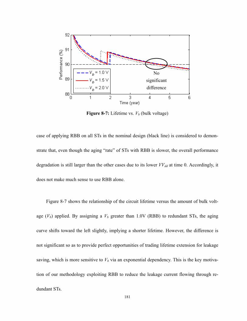
Figure 8-5: Aging behaviors of PMOS transistors with different Vth values ........................178
Figure 8-6: Comparison of aging behaviors with various settings .......................................180
Figure 8-7: Lifetime vs. Vb (bulk voltage) ............................................................................181
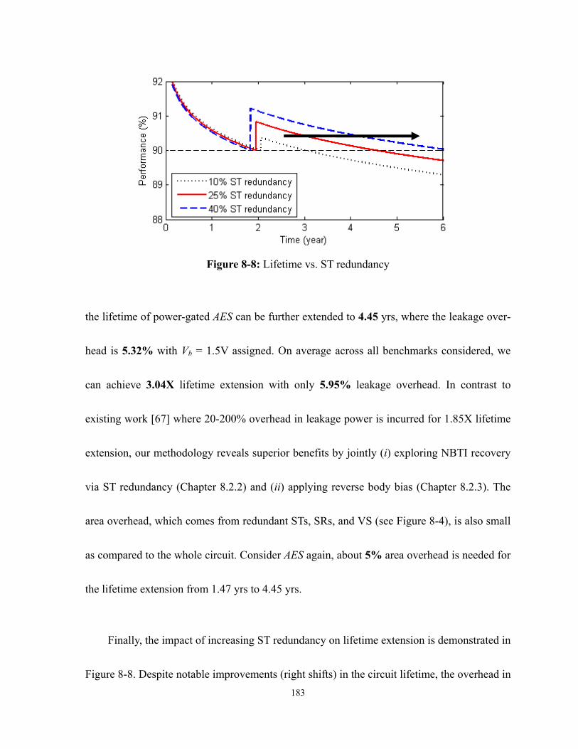
Figure 8-8: Lifetime vs. ST redundancy ...............................................................................183
xii
List of Tables
Table 3-1: MEI and MMI of gates in Figure 3-5: the second and third columns are for gates in Figure 3-5(a), the fourth and fifth for gates in Figure 3-5(b), and the sixth to eight for gates in Figure 3-5(c). ..........................................................47
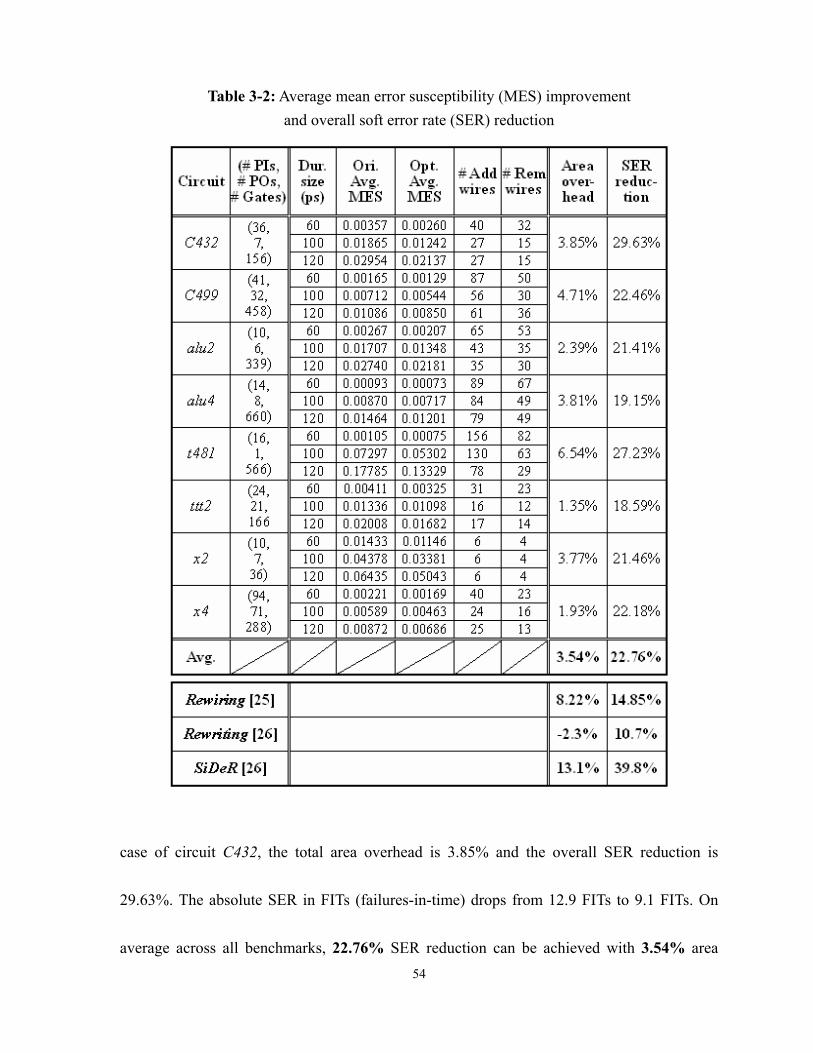
Table 3-2: Average mean error susceptibility (MES) improvement and overall soft error rate (SER) reduction............................................................54
Table 4-1: Average mean error susceptibility (MES) improvement and overall soft error rate (SER) reduction............................................................80
Table 5-1: Average mean error susceptibility (MES) improvement and overall soft error rate (SER) reduction..........................................................111
Table 6-1: Recovery of NBTI-induced performance degradation ........................................136
Table 7-1: Aging-aware timing analysis with and without path sensitization considered ....145
Table 7-2: Aging-aware timing optimization with path sensitization considered.................158
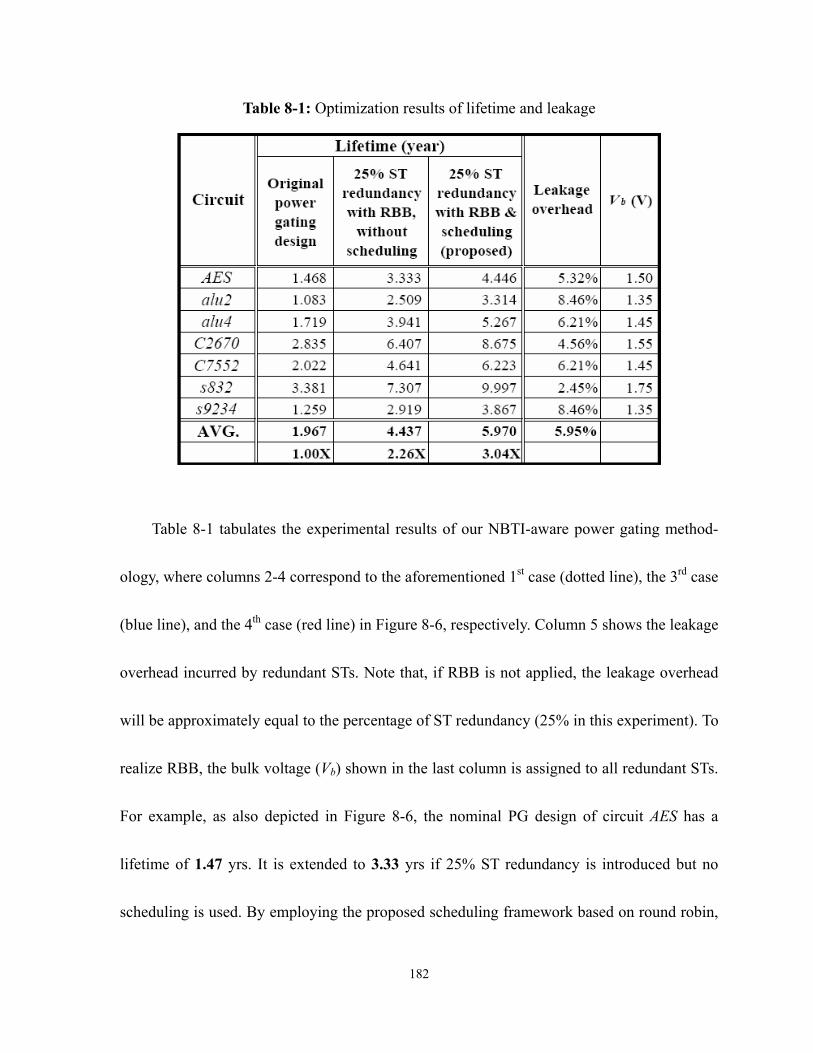
Table 8-1: Optimization results of lifetime and leakage .......................................................182
1
Chapter 1 Introduction
1.1 Thesis Motivation
Circuit reliability, usually measured by failure-in-time (FIT), has become a critical chal-
lenge for achieving robustness in nanoscale designs. The 2009 International Technology
Roadmap for Semiconductor (ITRS) [1] projects that the long-term reliability of sub-100nm
integrated circuits is on the order of 1000 FITs (failures in a billion hours). Soft errors, proc-
ess variations, and device aging phenomena are currently some of the main factors in reli-
ability degradation. With the continuous scaling of transistor dimensions, soft errors, which
cause unpredictable transient circuit failure, are becoming increasingly dominant for func-
2
tional reliability concerns [2]. On the other hand, device aging phenomena, which cause
significant loss on circuit performance and lifetime, are becoming increasingly dominant for
temporal reliability concerns [3]. Therefore, the need of an optimization flow considering
soft errors and aging effects in early design stages emerges.
A radiation-induced charged particle passing through a microelectronic device ionizes
the material along its path and generates free pairs of electrons and holes. The free (ionized)
carriers deposited around the particle track can be attracted or repelled by an internal electric
field of the device and lead to an electrical pulse, referred to as a single-event transient (SET)
or a glitch. A single-event upset (SEU) or a soft error refers to transient bit corruption that
occurs when a single-event transient is large enough to flip the state of a storage node. The
rate at which soft errors occur is called soft error rate (SER).
Traditionally, soft errors in both static and dynamic memories have drawn much atten-
tion due to their regularity and vulnerability. Unlike SETs in logic which need to be propa-
gated to outputs before being captured, soft errors happen in memories as long as particles
(with high enough energy) strike. During SET propagation, three mechanisms used to pro-
vide logic circuits with effective protection against soft errors:
3
1) Logical masking: A SET which is not on a sensitized path from the location where it
originates is logically masked. Once a SET is logically masked, it no longer has any in-
fluence on the target circuit; i.e., both of its amplitude and duration become zero.
2) Electrical masking: A SET which is attenuated and becomes too small in amplitude or
duration to be latched is electrically masked. While a SET may be latched if its attenu-
ated amplitude and duration are still large enough, electrical masking can reduce the
overall impact of SETs.
3) Latching-window (timing) masking: A SET which does not arrive “on time” is also
masked, depending on the setup and hold times of the target memory element. The basic
condition for a SET to be latched is to have its duration greater than the sum of setup
and hold times and to reach the memory element during the latching window.
These three mechanisms prevent some SETs from being latched and alleviate the effects
of soft errors in digital systems. However, continuous scaling trends have negative impact on
these masking mechanisms. Decreasing gate count and logic depth in super-pipeline stages
reduce the probability of logical masking since the path from where a SET originates to a
latch is more easily sensitized. Lower supply voltage and node capacitance needed by ul-
4
tra-low power designs not only decrease the critical charge for SETs, but also diminish the
pulse attenuation due to electrical masking. Higher clock frequency increases the number of
latching windows per unit of time and thus facilitates SET latching. As a result, soft errors in
logic become as great of a concern as in memories, where soft errors can be mitigated by
conventional error detecting and correcting codes. A recent study [4] showed that soft errors
significantly degrade the robustness of logic circuits, while the nominal SER of SRAMs
tends to be nearly constant from 130nm to 65nm technologies. Unless explicitly dealt with,
the SER of logic circuits was predicted to be comparable to that of unprotected memory
elements by 2011 [5]. Therefore, not only mission-critical applications, but also mainstream
commercial applications should be capable of soft error tolerance/resilience.
As for device aging, negative bias temperature instability (NBTI) on which this thesis
work focuses is known for prevailing over other device aging phenomena. NBTI [6] is a
PMOS aging phenomenon that occurs when PMOS transistors are stressed under Negative
Bias (Vgs = -Vdd) at elevated Temperature. NBTI-induced PMOS aging refers to the genera-
tion of interface traps along the silicon-oxide (Si-SiO2) interface due to the dissociation of
Si-H bonds. These traps manifest themselves as an increase in the magnitude of PMOS
5
threshold voltage (|Vth|, as much as 50mV over 10 years [7]), and in turn slow down the rising
propagation of logic gates. If the performance degradation continues and finally exceeds a
tolerable limit, the circuit lifetime will also be influenced since the timing specification is no
longer met. In contrast, the aging mechanism can be partially recovered by annealing gener-
ated interface traps when the stress condition is relaxed (Vgs = 0).
At traditional technology nodes, the NBTI problem is not so severe because the electric
field across gate oxide is small. However, as technology scaling proceeds aggressively, e.g.,
thinner gate oxide without proportional downscaling of supply voltage and higher operating
temperature due to higher power density, the dissociation of Si-H bonds is accelerated and
thus, the rate of NBTI-induced performance degradation is getting faster. Experiments on
PMOS aging [8] indicate that NBTI effects grow exponentially with thinner gate oxide and
higher operating temperature. If the thickness of gate oxide shrinks down to 4nm, the circuit
performance can be degraded by as much as 15% after 10 years of stress and lifetime will be
dominated by NBTI [9].
In addition to the oxide thickness and operating temperature, NBTI-induced perform-
ance degradation strongly depends on the amount of time during which a PMOS transistor is
stressed. In [10][11][12], the increase in threshold voltage has been demonstrated to be a
6
logarithmic function of the corresponding stress time. A PMOS under DC stress (i.e., duty
cycle = 1) suffers from static NBTI and ages very rapidly. Under a real AC stress condition
(i.e., duty cycle < 1), the NBTI impact is periodical and can be recovered, which results in a
lower extent of degradation. The stress time of a PMOS under AC stress is associated with its
stress probability, that is, the probability that Vgs is equal to -Vdd. For a NAND gate with
parallel pull-up PMOS transistors, the stress probability of any PMOS is simply the probabil-
ity of its input signal being logic “0”; for a NOR gate with series pull-up PMOS transistors,
the stress probability of a PMOS is the product of signal probabilities of its input and input(s)
to its upper PMOS transistor(s) in the stack. This parameter, based on the circuit topology
and input vectors, is distributed non-uniformly from transistor to transistor. The asymmetric
distribution may lead to 2-5X difference in the degradation rate of threshold voltage [13].
1.2 Thesis Overview and Contribution
Having discussed the importance of soft errors and NBTI in logic which motivates the
work on “reliability aware circuit optimization” (as it is titled), the main goal of this dis-
sertation research is to develop a low-cost, integrated framework that, given a logic circuit,
7
can optimize both its (i) functional reliability by reducing the overall SER and (ii) temporal
reliability by mitigating NBTI-induced performance degradation.
The scope of my thesis for SER reduction is outlined in Figure 1-1. Three approaches
for SER reduction are presented. The first one, based on redundancy addition and removal
(RAR), estimates the effects of redundancy manipulations and accepts only those with posi-
tive impact on circuit SER. Several metrics and constraints are proposed to guide the RAR
algorithm toward SER reduction in an efficient manner. The second approach, based on
selective voltage scaling (SVS), assigns a higher supply voltage to gates that have large error
impact and contribute most to the overall SER. The number of gates operating at the higher
voltage level, positively correlated with the power overhead, can be bounded by the appro-
priate use of level converters. The third approach, based on clock skew scheduling (CSS),
abcdO
123
1.0V 1.2VRedundancy addition and removal (RAR) changes the structure of the logic block
Selective voltage scaling(SVS) involves modification
on the power distribution
Clock skew scheduling(CSS) involves modification
on the clock network
Figure 1-1: Thesis scope for SER reduction
8
adjusts the arrival times of clock signals to memory elements (latches or flip-flops) such that
the probability of capturing unwanted transient pulses is decreased, as a result of more latch-
ing-window masking.
The major advantages over existing techniques are twofold: (i) lower design costs and
(ii) compounding results. Unlike some of existing SER reduction techniques based on dupli-
cation or resizing, which monotonically increase hardware resources without eliminating any,
the RAR-based approach focuses on restructuring the combinational block of a logic circuit
and incurs very little area overhead. By bounding the number of gates operating at high
supply voltage using level converters, the SVS-based approach significantly decreases the
power overhead and introduces only marginal delay penalty. As a post-processing procedure,
the CSS-based approach involves minor degree of clock network modification without
touching the logic block and thus, existing SER benefits from the two aforementioned ap-
proaches or other techniques such as duplication and resizing, if applied, will not be affected.
The scope of my thesis for NBTI mitigation is outlined in Figure 1-2. Joint logic re-
structuring and pin reordering are first exploited to combat performance degradation. Based
on detecting functional symmetries and transistor stacking effects, the proposed methodology
involves only wire perturbation and introduces no gate area overhead; therefore it can be
9
adopted as a pre-processing step when considering path sensitization for more accurate opti-
mization. It has been shown that mitigating aging effects while ignoring path sensitization
may lead to underestimation of circuit lifetime, thus pointing to the need of considering path
sensitization for aging-aware optimization when the impact of device aging is getting severe.
Finally, by exploring the recovery mechanism of NBTI, a scheduling algorithm for minimiz-
ing the NBTI effects on sleep transistors of a power-gated circuit is developed to extend its
lifetime for a longer period of reliable operation.
The salient feature of overall research contributions is that none of the reliability-aware
abcdO
123
Virtual VDD
Sleep
Joint logic restructuring (LR) and pin reordering (PR) for
the combinational block Consider path sensitization for more accurate and effective optimization
Redundant sleep transistors with RBB for
the power gating network
Figure 1-2: Thesis scope for NBTI mitigation
10
optimization techniques described above involves aggressive changes in logic circuits – all of
them incur favorable and affordable design penalties, while remarkably improving circuit
reliability. Furthermore, since all these proposed approaches can be embedded in existing
design flows, they can synergistically provide additive improvements when used together or
in conjunction with other techniques.
The rest of this dissertation is organized as follows: Chapter 2 reviews the background
of reliability modeling and analysis for SER (Chapter 2.1) and for NBTI (Chapter 2.2), and
also gives an overview of related work on SER reduction and NBTI mitigation. Three ap-
proaches for SER reduction based on redundancy addition and removal, selective voltage
scaling, and clock skew scheduling are presented in Chapter 3, Chapter 4, and Chapter 5,
respectively. A NBTI mitigation framework employing joint logic restructuring and pin
reordering is explained in Chapter 6; the NBTI-aware methodology is extended to consider
path sensitization, which is shown in Chapter 7; in Chapter 8, a novel strategy addressing the
NBTI issue in power-gated circuits is proposed. Finally, Chapter 9 summarizes this thesis
work.
11
Chapter 2 Background and Related Work
Used throughout this dissertation for our objective of reliability optimization, the mod-
eling and analysis frameworks for SER and NBTI are introduced in Chapter 2.1 and Chapter
2.2, respectively. Each of them is followed by a general statement of the corresponding opti-
mization problem and ends up with an overview of prior solutions.
2.1 Soft Error Rate (SER) Modeling and Analysis
Analyzing the soft error rate of a circuit accurately and efficiently is a crucial step for
SER reduction. Intensive research has been done so far in the area of SER modeling and
analysis. Among various existing modeling frameworks, we choose the symbolic one pre-
12
sented in [14]-[19] as the SER analysis engine. This symbolic SER analyzer, which provides
a unified treatment of three masking mechanisms through decision diagrams, enables us to
quantify the error impact and the masking impact of each gate in logic circuits. Hence, all
masking mechanisms, rather than one or two of them, are jointly considered as criteria for
SER reduction. To model a transient glitch originating at gate G to be latched at output F, the
following events can be defined:
A (Amplitude condition): The amplitude of a glitch at the output is larger than the
switching threshold of the latch (if the correct output value is “0”) or smaller than
the switching threshold (if the output value is “1”).
D (Duration condition): The duration of a glitch at the output is larger than the sum of
setup and hold times of the latch.
T (Timing condition): The glitch appears at the output on time; more specifically, it
satisfies the setup time and hold time requirements when the rising edge of the
clock occurs.
In this model, logical and electrical masking are implicitly included in A and D, while
latching-window masking is included in T. More formally, one can express these events as
13
follows:
A: A > Vs (if the correct output is “0”) or
A < Vs (if the correct output is “1”)
where A is the amplitude of the glitch and Vs is the switching threshold of the latch.
D: D > tsetup + thold
where D is the duration of the glitch, and tsetup and thold are the setup and hold times
of the latch.
T: t ∈ [T + thold – tp – D, T – tsetup – tp]
where t is the time when the initial glitch occurs, tp is the propagation delay from
gate G to output F, and T is the moment of a latch trigger (i.e., a clock edge).
The three events are necessary conditions for a soft error to happen. In addition, D is
satisfied only if A is satisfied (i.e., D ⊂ A). Under the assumption that t is uniformly distrib-
uted [20], the probability that a soft error occurs can be derived as:
P(A ∩ D ∩ T) = P(D ∩ T) = P(T | D)⋅P(D)
( )
∑
∑
⎟⎟⎠
⎞⎜⎜⎝
⎛=Ρ⋅
−+−
=
=Ρ⋅=−−−−+∈Ρ=
kk
initclk
holdsetupk
kkkpsetupphold
DDdT
ttD
DDDDttTDttTt
)()(
)()],[((1)
14
where {Dk} is the set of possible glitch durations, Tclk is the clock period, dinit is the initial
glitch duration, and t is uniformly distributed in the interval [T, T + Tclk – dinit].
Equation (1) is the worst-case derivation where [T + thold – tp – D, T – tsetup – tp] lies in [T,
T + Tclk – dinit], leading to the largest overlap between two intervals. In other words, the error
probability obtained by Equation (1) provides an upper bound on SER analysis. To find out
the possible values for duration, {Dk}, the attenuation model in [20] depending mainly on
gate propagation delay is used. To determine the probability of having a glitch with duration
Dk, the authors of [14][15] employ binary decision diagrams (BDDs) and algebraic decision
diagrams (ADDs). The detailed methodology of [14][15] is described next.
Terminal node “0” of the ADD associated with a gate represents all cases where a glitch
is logically or electrically masked; other terminal nodes represent the remaining values for
duration or amplitude after a glitch passes through the gate. The initial ADD of each gate is
built for the glitch originating at that gate. It consists of only one terminal node – initial
duration or amplitude value. These initial ADDs are propagated to respective fanout gates,
which use them to create new ADDs based on the attenuation model and related sensitization
BDDs.
15
Sensitization BDDs include information about logical masking. The sensitization BDD
of gate G to gate G’ is just the Boolean difference of G’ with respect to G (∂G’/∂G). Input
vectors that make the sensitization BDD of path G G’ go to terminal node “0” logically
mask glitches from gate G at gate G’. Therefore, only paths ending up in terminal node “1”
of the sensitization BDD and a node different from “0” of the associated ADD, need to be
considered for calculating new values relying on the attenuation model. All other cases,
which indicate either logical or electrical masking, go to terminal node “0”. Figure 2-2 dem-
onstrates the overall process of building duration ADDs for a glitch originating at gate G2 in
Figure 2-1.
Figure 2-1: An example circuit (C17) from the ISCAS’85 benchmark suite
16
Based on Equation (1), a key metric, mean error susceptibility (MES), for evaluating the
soft error rate of a circuit can be defined as follows: For each primary output Fj, initial dura-
tion d and initial amplitude a, MES(Fj) is the probability of output Fj failing due to errors at
internal gates. More formally, MES(Fj) can be expressed as:
fG
n
k
n
iij
adj nn
adglitchinitfailsGfailsFF
f G
⋅
=∩Ρ=∑∑
= =1 1,)),(_(
)MES( (2)
where nG is the cardinality of the set of internal gates in the circuit, {Gi}, and nf is the cardi-
nality of the set of input probability distributions, {fk}.
In [14], the authors compute the MES value of each primary output in combinational
logic for a discrete set of pairs (d, a) of initial glitch durations and amplitudes. Therefore, the
probability of output Fj failing due to glitches with various durations and amplitudes at dif-
Figure 2-2: Duration ADDs for a glitch originating at gate G2, and passing through gates G3 and G5, respectively
17
ferent internal gates is:
∑∑ Δ⋅+Δ⋅+
−⋅−Δ⋅Δ=Ρ
n m
anadmdjj F
aaddadF )(MES
)()()( minmin ,
minmaxminmax(3)
Finally, the soft error rate (SER) of primary output Fj can be derived as:
CIRCUITEFFPH ARR)()(SER ⋅⋅⋅Ρ= jj FF (4)
where RPH is the particle hit rate per unit of area, REFF is the fraction of particle hits that
result in charge disturbance, and ACIRCUIT is the total silicon area of the circuit.
2.1.1 Problem Statement
Typically, two types of methods are used for soft error hardening, namely, SER reduc-
tion. The first one, fault avoidance, consists in minimizing the occurrence of SETs at most
sensitive nodes, which in effect reduces SET generation. The second one, fault correction,
attempts to maximize the probabilities of three masking mechanisms, which reduces the
likelihood of generated SETs being latched. The objective of our SER reduction framework,
as explained later in Chapter 3 - Chapter 5, is to achieve the highest level of soft error toler-
ance by enhancing the circuit robustness/resilience to SETs/SEUs while incurring relatively
low design penalties. On one hand, belonging to the first category (fault avoidance), we
manipulate the operating voltage for smaller SET generation so as to make circuits more
18
robust to particle hits. On the other hand, belonging to the second category (fault correction),
we modify the logic structure and clock network for higher masking probabilities so as to
make circuits more resilient to already-existing SETs and SEUs as a result of particle hits.
2.1.2 Prior Work on SER Reduction (for Soft Error Tolerance)
Triple modular redundancy (TMR), consisting of three identical copies of an original
circuit feeding a majority voter, is the most well-known technique to realize soft error toler-
ance. But TMR is extremely expensive and not necessary for transient faults. To reduce the
overall cost, partial duplication [21] and gate resizing [22] strategies target only nodes with
high error susceptibility and ignore nodes with low error susceptibility. A potentially large
overhead in area and power is still needed for a higher degree of soft error tolerance. In [23],
voltage assignment is exploited to enhance the circuit robustness to soft errors. This method
trades power penalty for SER reduction by applying a higher supply voltage to a certain
portion of gates. A related method [24] uses optimal assignments of gate size, supply voltage,
threshold voltage, and output capacitive load to get better results with smaller area overhead.
Nevertheless, such a method increases design complexity and may make resulting circuits
hard to optimize at the physical design stage. Approaches based on rewiring or resynthesis
19
[25][26] can achieve relatively smaller SER improvement while incurring little overhead.
Sequential circuits, as opposed to combinational circuits, have received less attention in
terms of soft error tolerance. Since a sequential circuit has a feedback loop leading back to
state inputs of the circuit, it is possible that errors latched at state lines propagate through the
circuit for multiple clock cycles. Therefore, SER-aware sequential circuit optimization
should consider transient faults during successive cycles. The intuitive way to address this
problem is by replacing sequential elements with hardened latches or flip-flops that are less
sensitive to soft errors, as developed in [27]. A flip-flop sizing scheme [28] increases the
probability of latching-window (timing) masking by lengthening the latching window inter-
vals of vulnerable flip-flops. However, this scheme does not take into account logical mask-
ing and electrical masking, which are also important factors in determining circuit SER. To
deal with this, the authors of [29] proposed a hybrid approach combining gate and flip-flop
sizing (selection) to obtain more SER reduction. In [30], gates are locally relocated such that,
for each gate, delays to different outputs are balanced as much as possible. In effect, this
strategy minimizes the probability that an error originating at a gate is registered by any of
the flip-flops. The error, however, may reach more than one output simultaneously due to
balanced path delays and be registered by multiple flip-flops, resulting in so-called multi-
20
ple-bit upsets (MBUs). For sequential circuits, MBUs imply that there will be multiple errors
propagating in subsequent cycles, further degrading circuit reliability. This is a crucial reli-
ability concern in sequential circuits that has not been addressed so far.
Instead of exploring spatial redundancy as mentioned above, several techniques for soft
error hardening based on temporal redundancy were presented in [31][32]. Nevertheless,
such techniques employing time-domain majority voting are very sensitive to delay varia-
tions and fail to cope with large-duration SETs because a sufficiently large slack time is
required.
2.2 Negative Bias Temperature Instability (NBTI) Modeling and
Analysis
The NBTI modeling and analysis framework used in this work is the one developed in
[12][13][33][34]. The framework provides a mathematical model, taking into account both
aging and recovery mechanisms, for predicting the long-term PMOS degradation due to
NBTI.
21
First, the degradation of threshold voltage at a given time t can be predicted as:
n
nt
clkvth
TKV
2
2/1
2
1 ⎟⎟
⎠
⎞
⎜⎜
⎝
⎛
−⋅⋅
=Δβ
α (5)
where Kv is a function of temperature, electrical field, and carrier concentration, α is the
stress probability, n is the time-exponential constant, 0.16 for the used technology, and
tCt
TCt
ox
clket ⋅+
−⋅⋅⋅+⋅−=
2)1(2
1 21 αξξβ
The detailed explanation of each parameter can be found in [33].
Next, the authors of [34] simplify this predictive model to be:
nnnth tbtbV )( ⋅⋅=⋅⋅=Δ αα (6)
where b = 3.9×10⁻³ V·s-1/6.
Finally, the rising propagation delay of a gate through the degraded PMOS can be de-
rived as a first-order approximation:
npp ta )( ⋅⋅+=′ αττ (7)
where ιp is the intrinsic delay of the gate without NBTI degradation and a is a constant.
We apply Equation (7) to calculate the delay of each gate under NBTI, and then estimate
the performance of a circuit. The coefficient a in Equation (7) for each gate type and each
22
input pin is extracted by fitting SPICE simulation results in 65nm, Predictive Technology
Model (PTM) [35]. The simplified model successfully analyzes the long-term behavior of
NBTI-induced PMOS degradation with negligible error, within 5% versus the cycle-by-cycle
(short-term) simulation. Hence, the performance (timing) estimation in our methodology is
more accurate and efficient than those in existing techniques which ignore the recovery
mechanism or employ expensive cycle-by-cycle simulations. For more details about this
mathematical NBTI model, please refer to [12][13][33][34].
2.2.1 Problem Statement
The objective of our NBTI mitigation framework, as explained later in Chapter 6 -
Chapter 8, is to minimize the circuit delay under NBTI over 10 years while incurring as little
area overhead as possible. We manipulate stress probabilities by using logic restructuring
and pin reordering such that NBTI effects on those gates (transistors) along timing-critical
paths can be reduced. Subsequently, transistor resizing is integrated for further reduction in
NBTI-induced performance degradation, with less design penalty than stand-alone
NBTI-aware resizing, especially when path sensitization is considered for more accurate
optimization.
23
2.2.2 Prior Work on NBTI Mitigation (against NBTI-Induced Performance
Degradation)
Traditional design methods add guard-bands or adopt worst-case margins to account for
aging phenomena, which in practice imply over-design and may be cost-expensive. To avoid
overly conservative design, the mitigation of NBTI-induced performance degradation can be
formulated as a timing-constrained area minimization problem with consideration of NBTI
effects. Recent NBTI-aware techniques basically follow this formulation. The authors of [36]
proposed a gate sizing algorithm based on Lagrangian relaxation (LR). The LR-based algo-
rithm determines the optimal values of gate sizes, which are assumed to be continuous, by
solving a non-linear area minimization problem. An average of 8.7% area penalty is required
to ensure reliable operation for 10 years. Other methods related to gate sizing can be found in
[37][38][39].
A novel technology mapper considering signal probabilities for NBTI was developed in
[40]. This technique first characterizes each gate in a given standard cell library in terms of
its NBTI impact, as a function of its input signal probabilities. Then, the technology mapper
takes signal probabilities as one of the arguments when searching for the best matching in the
library. About 10% area recovery and 12% power saving are accomplished, as compared to
24
the most pessimistic case assuming static NBTI on all PMOS transistors in a design. In [41],
a reconfigurable flip-flop design based on time borrowing is introduced for aging detection
and correction. Among all of the aforementioned approaches, only the one in [39] considers
path sensitization for more accurate optimization. However, the approach involves path
enumeration (on a path-wise basis) of exponential complexity and is not scalable for large
benchmarks.
Instead of reducing NBTI effects during active mode as described above, an idea of
NBTI-aware optimization during standby mode was presented in [42]. Input vectors for
minimum standby-mode leakage are selected to minimize PMOS aging. Moreover, for gates
that are deep in a large circuit and cannot be well controlled by primary input vectors, inter-
nal node control [43] intrusively assigns logic “1” to those gates if they are on the critical
paths. The logic “1” relaxes the stress condition and can thus relieve the NBTI impact. In
[44], power gating (PG) is exploited for aging optimization by shutting off the power supply
to a circuit. However, the continuous Vth degradation of sleep transistors during active mode
in the case of header-based PG design is ignored in [42][43][44].
25
SER REDUCTION
26
Chapter 3 SER Reduction via Redundancy Addition and Removal (RAR)
Before introducing the proposed SER reduction approaches, we define two metrics as-
sociated with SER analysis in the sequel. The first, mean error impact (MEI), characterizes
each gate in terms of its contribution to the overall SER; the second, mean masking impact
(MMI), characterizes each gate in terms of its capability of filtering glitches propagated
through its inputs.
Definition 1 (mean error impact): For each internal gate Gi, initial duration d and initial
amplitude a, mean error impact (MEI) over all primary outputs Fj that are affected by a
glitch occurring at the output of gate Gi is defined as:
fF
n
k
n
jij
adi nn
adglitchinitfailsGfailsFG
f F
⋅
=∩Ρ=ΜΕΙ∑∑
= =1 1,
)),(_()( (8)
27
where nF is the cardinality of the set of primary outputs in the circuit, {Fj}, and nf is the
cardinality of the set of input probability distributions, {fk}.
The MEI value of a gate quantifies the probability that at least one primary output is af-
fected by a glitch originating at this gate. The larger MEI a gate has, the higher the probabil-
ity that a glitch occurring at this gate will be latched. This implies that those gates with
higher MEI make the circuit more vulnerable to soft errors. Thus, it is beneficial for SER if
gates with large MEI are removed from the circuit.
We need the following notations for defining mean masking impact.
D(Gi): the attenuated duration of a glitch at gate Gi
C(Gi): the set of gates in the fanin cone of gate Gi
F(Gi): the set of gates in the immediate fanin of gate Gi
p(Gj, Gi): the set of gates on the paths between gates Gj and Gi
Definition 2 (mean error impact): For each internal gate Gi, initial duration d and initial
amplitude a, we define mean masking impact on duration (MMID) as:
dnn
GGG
fG
n
k
n
ji
adj
adi
f G
⋅⋅
→ΜΙ=ΜΜΙ∑∑
= =1 1
,D
,D
)()( (9)
28
where nG is the cardinality of C(Gi), nf is the cardinality of the set of input probability distri-
butions, {fk}, and MID(Gjd,a → Gi), masking impact on duration of gate Gi with respect to
(w.r.t.) gate Gj, denotes the absolute duration attenuation contributed by gate Gi on a glitch
with duration d and amplitude a originating at gate Gj. MID(Gjd,a → Gi) can be formally
defined as:
( )
( )∑ ∑
∑
∩∈
−⋅=∩=Ρ−
−⋅=∩=Ρ=
→ΜΙ
),(p)(F
,D
)()),(_)(D(
)()),(_)(D(
)(
ijil GGGG kkjkl
kkjki
iad
j
DdadglitchinitfailsGDG
DdadglitchinitfailsGDG
GG
(10)
where {Dk} is the set of possible values for glitch duration, as in Equation (1). The second
summation represents the total weighted attenuation attributed to gate Gi’s immediate fanin
gates on the paths between gates Gj and Gi, instead of just gate Gi itself. Intuitively, MID(Gjd,a
→ Gi) quantifies how much attenuation can be contributed to gate Gi only, on the duration of
glitches originating at gate Gj.
Example: In Figure 2-1, assume only one set of input probability distributions is applied to
the circuit: {P1 = 0.5, P2 = 0.5, P3 = 0.5, P4 = 0.5, P5 = 0.5} where Pi is the probability of
logic “1” for the ith primary input. The duration ADDs associated with mean masking impact
on duration of gate G5 are shown in Figure 3-1, where those values for attenuated duration in
the terminal nodes are assigned arbitrarily for the sake of simplicity. In the real case, the
29
values are found using the attenuation model presented in [20]. Given initial duration d and
initial amplitude a, the mean masking impact on duration of G5, MMID(G5d,a), is computed as
follows. Since there are three gates G1, G2 and G3 in G5’s fanin cone, there will be three
masking impact values for MMID(G5d,a).
According to Figure 3-1(a), the masking impact on duration of gate G5 w.r.t. gate G1 is:
dddd
dddADD
dddADDdADD
GG
G
GGGG
ad
127)
32(
85)0(
83
)()(
)32()
32()0()0(
)(
1
5151
5,
1D
=−+−=
−⋅→Ρ−
−⋅→Ρ+−⋅→Ρ=
→ΜΙ
→→
(11)
According to Figure 3-1(b), the masking impact on duration of gate G5 w.r.t. gate G2 is:
(a) Duration ADDs for path G1 G5 (b) Duration ADDs for path G2 G3 G5
(c) Duration ADDs for path G3 G5
Figure 3-1: Duration ADDs associated with mean masking impact on duration of gate G5
30
ddd
dddddd
dddADDdADD
dddADDdADD
GG
GGGG
GGGGGG
ad
61
32
65
)32(
21)0(
21)
94(
83)0(
85
)32()
32()0()0(
)94()
94()0()0(
)(
3232
532532
5,
2D
=−=
−−−−−+−=
−⋅→Ρ−−⋅→Ρ−
−⋅→Ρ+−⋅→Ρ=
→ΜΙ
→→
→→→→
(12)
According to Figure 3-1(c), the masking impact on duration of gate G5 w.r.t. gate G3 is:
dddd
dddADD
dddADDdADD
GG
G
GGGG
ad
21)
32(
43)0(
41
)()(
)32()
32()0()0(
)(
3
5353
5,
3D
=−+−=
−⋅→Ρ−
−⋅→Ρ+−⋅→Ρ=
→ΜΙ
→→
(13)
One can note that the gate at which a glitch originates has no masking impact on that
glitch. In Equation (12), the third and fourth terms are the amount of attenuation attributed to
gate G3 and should be subtracted. By Equation (9), we can obtain the mean masking impact
on duration of gate G5:
125
321
61
127
3)()()(
)(
5,
3D5,
2D5,
1D
,5D
=++
=
→ΜΙ+→ΜΙ+→ΜΙ=
ΜΜΙ
d
ddd
dGGGGGG
Gadadad
ad
(14)
Similarly, we can also define mean masking impact on amplitude (MMIA) by replacing
the normalization factor, d, in (3) with the initial amplitude, a, and {Dk} in (4) with {Ak}, the
set of possible values for glitch amplitude. Basically, the associated amplitude ADDs for
mean masking impact on amplitude of gate G5 are isomorphic to those duration ADDs in
31
Figure 3-1. The only difference is in the values of terminal nodes. As a result, the way to
compute mean masking impact on amplitude of G5 is the same as shown in the above exam-
ple – except that one has to replace the attenuated duration (Dk) with the attenuated amplitude
(Ak). We found that the duration of a glitch is proportional to the probability of a soft error
being registered, but the amplitude of a glitch is not. Therefore, it makes sense to use only
mean masking impact on duration (MMID) as a guideline for SER reduction.
The MMI value of a gate, defined by Equation (9) and shown in the above example,
denotes the normalized expected attenuation on the duration (or amplitude) of all glitches
passing through the gate. Every MMI value ranges from 0 to 1 as a result of normalization.
The larger MMI a gate has, the more capable of masking glitches this gate is. A gate with
MMI equal to 0 will not attenuate any glitch at all; in contrast, a gate with MMI equal to 1
will entirely mask glitches passing through it. This implies that those gates with higher MMI
make the circuit more robust to soft errors. In general, high MMI of a gate is due to its large
gate delay or considerable effect of logical masking on the gate. Thus, it is also beneficial for
SER if gates with large MMI are kept in the circuit.
32
3.1 RAR-Based Approach for SER Reduction
In this subchapter, we present our SER reduction approach based on redundancy addi-
tion and removal (RAR). RAR is a logic minimization technique which performs a series of
wire/gate addition and removal operations by searching for redundant wires/gates in a circuit.
Candidate wires for addition can be identified according to the mandatory assignments made
during automatic test pattern generation (ATPG). Mandatory assignments [45] are those
value assignments which are required for a test to exist and must be satisfied by any test
vector. For example in Figure 3-2(a), the mandatory assignments for gate G6 stuck-at-1 fault
are {f = 1, G3 = 1, G4 = 0, G6 = 0}, from which we can get the implications {d = 0, G1 = 0, G2
= 0, G5 = 0}. If a wire from gate G5 to gate G9 is added into the circuit, there will be a con-
flicting assignment because gate G5 should be set to be “1” to make gate G6 stuck-at-1 fault
observable at outputs. So wire G5 G9 is a candidate for wire addition.
One still needs to check if the candidate wire is indeed redundant; i.e., the wire does not
change the circuit functionality. In the above example, wire G5 G9 is redundant. The newly
added wire could cause one or more existing irredundant wires to become redundant (re-
movable). ATPG is again used for redundancy checking of each wire except the one just
inserted (e.g., wire G5 G9 in Figure 3-2(b)) by finding compatible mandatory assignments.
33
If a set of mandatory assignments for a wire cannot be derived, the wire is said to be redun-
dant and can be removed. Consider the same example in Figure 3-2: after adding wire G5
G9 into the circuit, wires G1 G4 and G6 G7 become redundant as compatible mandatory
assignments do not exist for both of them. So they can be removed, as shown in Figure
3-2(b).
Note that gates with only one fanin and gates without fanout can also be deleted. Figure
3-2(c) shows the resulting circuit after redundancy removal. The circuit becomes smaller if
the removed redundancies are more than the added redundancies. For the goal of logic opti-
mization, the wire addition and removal procedures iterate until no further improvement can
be found.
For our objective of SER reduction, using RAR in an unsystematic manner may increase
SER by reducing the number of gates or the depth of circuits: a smaller gate count will affect
(a) The original circuit (b) The circuit after redundancy
addition (G5 G9)
(c) The circuit after redundancy
removal (G1 G4 and G6 G7)
Figure 3-2: An example of redundancy addition and removal [46]
34
the impact of logical masking, while smaller logic depth will reduce the impact of both logi-
cal and electrical masking. The basic principle of our RAR-based approach is to keep
wires/gates with high masking impact and to remove wires/gates with high error impact.
The RAR technique has two major parts: wire addition and wire removal. Each wire ad-
dition step is followed by a wire removal step, irrespective of whether or not there are any
removable wires other than the added one available. For logic minimization, where the goal
is the total literal count, it is easy to track the change in the number of literals after an itera-
tion of addition and removal by simply calculating the number of added and removed
wires/gates. However, for SER reduction, it is not efficient to track the change in the soft
error rate of a circuit by re-computing it every time. Instead, during each step of wire addi-
tion/removal, we define criteria or constraints to guide us in the wire addition/removal proc-
ess and check whether the step is advantageous for SER reduction.
Several constraints on the RAR algorithm are introduced to ensure that our proposed
approach can significantly mitigate the soft error rate of a logic circuit. In the beginning of
this chapter, we have demonstrated the relationship between MEI/MMI and circuit vulner-
ability/robustness. Intuitively, one can use MEI and MMI as metrics to guide RAR toward
SER reduction.
35
3.1.1 Wire Addition Constraint
Let wire w (s t) be an addible (redundant) candidate wire whose source node is gate s
and destination node is gate t, as shown in Figure 3-3. The following three effects take place
after adding wire w into the circuit:
1) The MEI values of gate s and its fanin neighbors are likely to increase because the new
connection w from gate s to gate t provides an additional path for propagating erroneous
values to primary outputs.
2) The MEI values of fanin neighbors of gate t are likely to decrease because, to a certain
extent, the new connection w logically masks glitches from those fanin neighbors. The
MEI values of some gates which are in the fanin cones of both gates s and t may in-
MEI(s), MEI(a), MEI(b), and MEI(fanin neighbors of gates a and b) ↗ (ADVERSE!)
MMI(t) ↗
MEI(c), MEI(d), and MEI(fanin neighbors of gates c and d) ↘
Figure 3-3: Changes in MEI and MMI after adding wire w (s t)
36
crease, but these increases are incorporated into effect 1) above.
3) The MMI value of gate t becomes larger due to increased logical masking and propaga-
tion delay. The MMI values of fanout neighbors of gate t may also change (increase or
decrease), but these changes will not degrade the circuit robustness since fewer glitches
(with smaller duration and amplitude) pass through gate t.
Based on the definitions of MEI and MMI, the first effect (shown within the highlighted
region in Figure 3-3) is adverse, but the second and third ones are beneficial for SER reduc-
tion. Hence, we introduce a constraint to minimize the adverse effect.
Constraint 1 (wire addition constraint): Wire w (s t) can be added into the circuit if
MEI(t) < T1 and MMID(t) > T2 where T1 and T2 are pre-specified thresholds.
Intuitively, those wires having small MEI and large MMID for their destination gates can
be added. This constraint will keep gates with large MMI in the circuit. To simplify the
following discussion without loss of generality, we omit initial duration d and amplitude a
from the notations of MEI (Equation (8)) and MMI (Equation (9)), but keep in mind that they
actually exist.
37
After adding wire w into the circuit, no matter how small MEI(s) is, a complete glitch
with the initial duration and amplitude is propagated from gate s to gate t once an effective
particle strikes gate s. That is, the resulting increase in error impact of gate s due to glitches
propagated along the new connection w does not depend on MEI(s). More precisely, assume
that the initial duration of a glitch occurring at gate s is d. After passing through gate t, the
attenuated duration of the glitch can be quantified as:
[ ])(1 D tdd ΜΜΙ−⋅=′ (15)
If d’ is smaller than or equal to the sum of setup and hold times, the glitch will be
masked; otherwise, the increase in MEI(s) due to the addition of wire w is estimated to be:
[ ]
[ ])(1)(
)(1)()()(
D
D
ttd
tdtddts
ΜΜΙ−⋅ΜΕΙ=
ΜΜΙ−⋅⋅ΜΕΙ=′
⋅ΜΕΙ=ΔΜΕΙ(16)
This observation is based on the fact that the duration of a glitch (if large enough) is
proportional to the probability of the glitch being latched. From Equation (16), one can
minimize the increases in the MEI values of gate s and its fanin neighbors by specifying a
sufficiently small T1 and a sufficiently large T2 for MEI(t) and MMID(t), respectively. Al-
though we can also specify additional thresholds for MEI(s) and MMID(s) to further mini-
mize the increases in the MEI values of those fanin neighbors, doing so greatly restricts the
38
search space for RAR and typically, does not lead to better results.
3.1.2 Wire Removal Constraint
Let wire w’ (u v) be a removable (redundant) candidate wire whose source node is
gate u and destination node is gate v, as shown in Figure 3-4. Three other effects take place
after removing wire w’ from the circuit:
1) The MEI values of gate u and its fanin neighbors are likely to decrease because errone-
ous values propagated along the removed connection w’ from gate u to gate v are elimi-
nated.
2) The MEI values of fanin neighbors of gate v are likely to increase because logical
MEI(u), MEI(a), MEI(b), and MEI(fanin neighbors of gates a and b) ↘
MMI(v) ↘(ADVERSE!)
MEI(c), MEI(d), and MEI(fanin neighbors of gates c and d) (ADVERSE!)↗
Figure 3-4: Changes in MEI and MMI after removing wire w’ (u v)
39
masking impact at gate v is decreased by the removal of wire w’.
3) The MMI value of gate v becomes smaller due to decreased logical masking. At the
same time, the MMI values of fanout neighbors of gate v may also change (increase or
decrease).
Based on the definitions of MEI and MMI, the first effect is beneficial, but the second
and third ones (shown within the highlighted region in Figure 3-4) are adverse for SER re-
duction. Hence, we set up two additional constraints: one is to maximize effect 1), the other
to minimize effects 2) and 3).
Constraint 2 (wire removal constraint I): Wire w’ (u v) can be removed from the circuit
if MEI(v) > T3 ≧ T1 and MMID(v) < T4 ≦ T2 where T3 and T4 are pre-specified thresholds.
Intuitively, those wires having large MEI and small MMID for their destination gates can
be removed. This constraint will try to remove gates with large MEI from the circuit. Again,
without loss of generality, we omit initial duration d and amplitude a, which actually exist,
from the notations of MEI and MMI. Similar to the argument for Equation (16), the decrease
in MEI(u) due to the removal of wire w’ is estimated to be:
[ ])(1)()( D vvu ΜΜΙ−⋅ΜΕΙ=ΔΜΕΙ (17)
40
From Equation (17), one can maximize the decreases in the MEI values of gate u and its
fanin neighbors by specifying T3 and T4 where T3 ≧ T1 and T4 ≦ T2. The lower bound for T3
and the upper bound for T4 are set such that we can gain more from wire removal (e.g.,
ΔMEI(u) in Equation (17)) than lose from wire addition (e.g., ΔMEI(s) in Equation (16)).
Constraint 3 (wire removal constraint II): Wire w’ (u v) can be removed from the circuit
if ( ) cvTvcvu <=Ρ )(ˆ across all probability distributions where u is the output value of gate
u, cv(v) is the controlling value of gate v, and Tcv is a pre-specified threshold.
The necessary condition of logical masking at gate v is that at least one of the side in-
puts must be the controlling value of gate v, expressed by cv(v). Side inputs are those inputs
on which no glitch is propagated. For instance, gate v in Figure 3-4 is assumed to be an OR
gate (i.e., cv(v) = 1). If a glitch is propagated from gate c to gate v and the output value of
gate u is “1”, the glitch will be logically masked by the controlling value “1” from gate u.
The higher probability of going to cv(v) gate u has, the more likely glitches from gate v’s
fanin gates (except gate u itself) will be logically masked at gate v. Therefore, this constraint
is introduced to minimize the loss on logical masking as a result of wire removal. When
( ))(ˆ vcvu =Ρ is large, wire w’ (u v) plays an important role in logically masking glitches at
gate v and should not be removed.
41
Furthermore, for some added wires, there may be more than one corresponding remov-
able wires which are mutually irredundant and cannot be removed together. In other words,
removing one redundant wire will cause another one(s) to become irredundant. We sort these
removable wires by the MEI values of their source gates, from the largest to the smallest. The
removable wire with the largest MEI value for its source gate will be removed first. We can
thus further maximize the beneficial effect 1) of wire removal and potentially remove gates
with large MEI.
3.1.3 Topology Constraint on Candidate Addition and Removal
Two types of mandatory assignments (MAs) are distinguished in the original RAR paper
[45]: backward MA and forward MA. If a mandatory assignment of gate G is obtained by
backward implication from G’s fanout gates, the mandatory assignment is a backward MA. If
a mandatory assignment of gate G is obtained by forward implication from G’s fanin gates,
the mandatory assignment is a forward MA. Assume that a pair of candidate wires for addi-
tion wa (s t) and for removal wr (u v) are extracted. Gate t either (i) has a backward MA
due to the redundancy checking of wire wr, or (ii) has to be a dominator of gate v along with
a forward MA. Here, gate D is said to be a dominator of gate G with respect to output O iff
42
all paths from G to O must pass through D. Also, we say that D dominates G or G is domi-
nated by D, with respect to O. For example in Figure 3-5(b), gate G7 is a dominator of gate
G2 w.r.t. output y while gate G6 is not, since G6 does not have to lie on the paths from G2 to y
(e.g., G2 G5 G7 y).
The aforementioned three constraints focus on finding redundant wires for addition and
removal such that the positive influences on circuit SER (e.g., ΔMEI(u) in Equation (17)) are
greater than the negative influences (e.g., ΔMEI(s) in Equation (16)). To satisfy ΔMEI(u) >
ΔMEI(s), however, these constraints filter out most candidate pairs falling into the second (ii)
category described above. The reason is that a dominator, which is closer to primary outputs,
has higher MEI than the gate being dominated [15]. Let wire wa (s t) for addition and wire
wr (u v) for removal be a candidate pair where gate t is a dominator of gate v. As in [45],
wires wa and wr are regarded as alternatives of each other and supposed to be implemented
(a) The original circuit with candidate
wire wa (G2 G5) for addition
(b) The circuit with candidate wire wr
(G1 G3) for removal after adding wire wa
(c) The resulting circuit
after removing wire wr
Figure 3-5: An example of Constraint 4 and the effect of redundancy on soft error robustness
43
together. Since gate t is a dominator and thereby MEI(t) is usually larger than MEI(v),
ΔMEI(s) in Equation (16) will be easily larger than ΔMEI(u) in Equation (17), too. More
specifically, given MEI(t) > MEI(v), T1 and T3 used in Constraint 1 and Constraint 2, MEI(v)
> T3 ≧ T1 > MEI(t) is never true, meaning that two constraints may not be met simultane-
ously and this pair of candidate wires (wa and wr) will be discarded. But such a pair is not
always adverse for SER. To keep such potential redundancy manipulations and explore more
solution space for our methodology, we introduce the last constraint.
Constraint 4 (topology constraint): Given candidate wire wa (s t) for addition and wire wr
(u v) for removal, the addition and removal steps can be performed together if gate t is a
dominator of gate v and also a dominator of gate u assuming wa and wr have been imple-
mented already.
Consider the circuit in Figure 3-5 where wire wa (G5 G7) is an alternative of wire wr
(G2 G4), which suggests that wa can be added for removing wr, as shown from Figure
3-5(a) to Figure 3-5(c). That is, wires wa and wr are recognized as a pair of candidates for
addition and removal, respectively. In this example, wire wa’s destination node, G7, is a
dominator of both gates G2 and G4 (as in Figure 3-5(c), after the current RAR operations).
Therefore, it is very likely that removal-of-wr-induced adverse impact, stemming from gates
44
G2 and G4, will be blocked at dominator G7 due to the addition of wire wa, which reflects
more logical masking, larger propagation delay and in effect, more electrical masking. This is
basically true if wire wa can be used to realize a more complex logic cell at gate G7 with
longer delay [47]. For instance, gate G7 in Figure 3-5(c) can be remapped with wire wa to a
3-input AND whose delay is 43.33ps, while its original realization (without wa) in Figure
3-5(a), a 2-input AND, has a delay of 34.67ps. The delay numbers are found using logical
effort [48] in 70nm Predictive Technology Model (PTM). As mentioned earlier, high MMI
results from large propagation delay or considerable logical masking. We can thus expect to
see a significant increase in the MMI value of gate G7, which has been known as a dominator
and will stop more error impact from those gates being dominated.
Note that one still needs to quantitatively check if such a pair of redundancy manipula-
tions is indeed beneficial. An extended strategy of estimation from Equations (16) and (17) is
discussed as follows. The basic idea is to look at the dominator only. In the case exemplified
by Figure 3-5, we check whether or not gate G7, given the addition of wire wa, is powerful
enough to block additional error impact as a result of wa-addition and wr-removal. More
precisely, the following steps need to be followed:
1) Update MMID(G7) locally and incrementally: To do this, we first renew the propagation
45
delay of gate G7, and apply the new delay on the attenuation model to recalculate
non-zero terminal nodes of those ADDs which have been propagated to G7. Next, the
ADD structures also need to be transformed; these transformations can be accomplished
incrementally because wire wa brings supplementary patterns of logical masking without
shrinking the original, i.e., one-way expansion of logical masking patterns. Then, we
propagate ADDs from gate G5 to gate G7 (along wire wa) and compute corresponding
new ADDs attenuated by G7. Finally, updated MMID(G7), denoted by MMID’(G7), can
be obtained.
2) Calculate the changes in MEI of gate G7’s immediate fanin neighbors, namely,
ΔMEI(G3), ΔMEI(G5), and ΔMEI(G6):
⎪⎪⎩
⎪⎪⎨
⎧
⎥⎦⎤
⎢⎣⎡ −′⋅=
ΔΔ
⎥⎦⎤
⎢⎣⎡ ′−⋅=Δ
)(MMI)(MMI)(MEI)(MEI)(MEI
)(MMI1)(MEI)(MEI
7D7D76
3
7D75
GGGGG
GGG
(18)
where ΔMEI(G3) and ΔMEI(G6) are advantageous and ΔMEI(G5) is disadvantageous.
The cumulative estimation of absolute MEI changes is:
∑Δ
)Δ+)Δ−)Δ=MEI
653 (MEI(MEI(MEI GGG (19)
For the same reason as in Constraints 1 and 2, those gates beyond the first-level (imme-
46
diate) fanin of the dominator are not taken into account in order to relax the restriction
on RAR, reduce the computational complexity and keep our methodology tractable.
This heuristic of considering only immediate fanin gates is experimentally verified to be
representative enough for analysis and estimation of impact on circuit SER.
3) Evaluate the validity of this candidate pair (wire wa for addition and wire wr for re-
moval):
⎪⎩
⎪⎨⎧ ≥∑
Δ
ra
ra
ww
ww
and discard Otherwise,
and accept ,0 IfMEI (20)
In wire addition and removal constraints, MMI does not require updating due to the fol-
lowing reasons: ΔMEI(s) in Constraint 1 is the worst-case (pessimistic) estimation, which is
reasonable to be used for estimating adverse effects; ΔMEI(u) in Constraint 2 is the aver-
age-case estimation, which is just suitable for estimating beneficial effects. In Equation (18),
ΔMEI(G3) and ΔMEI(G6) both belong to the second effect of wire addition. We do not con-
sider this beneficial effect when applying wire addition constraint (Constraint 1) so MMI
updating is not necessary. As for wire removal constraint, Constraint 3 has been introduced to
assist Constraint 2 in minimizing adverse effects of wire removal. Hence, we do not need
new MMI to estimate these effects, either.
47
Constraint 4 catches those candidates missed by the first three constraints, which allows
for higher likelihood to get a better solution. Table 3-1 lists the MEI and MMI values of gates
in Figure 3-5, where wires wa and wr are the current pair of candidates for addition and re-
moval, respectively. With a set of appropriate thresholds, it is obvious that wa and wr will be
filtered out by Constraints 1 and 2. However, this candidate pair satisfies Constraint 4 and
can be performed for a reduction of 33.2% in average MEI w.r.t. output y, equivalent to
33.2% reduction in SER of output y. As it can be seen, the MEI values of gates in the fanin
cone feeding wire wa (e.g., G2 and G5) increase marginally while those in the original fanin
cone of gate G7 (e.g., G3, G4 and G6) decrease significantly. According to the test results with
other benchmark circuits, most of the cases satisfying Constraint 4 are beneficial for SER as
Table 3-1: MEI and MMI of gates in Figure 3-5: the second and third columns are for gates in Figure 3-5(a),
the fourth and fifth for gates in Figure 3-5(b), and the sixth to eight for gates in Figure 3-5(c).
48
long as their dominators have sufficient (>20%) increases in MMI.
Constraint 4, exemplified by Figure 3-5, particularly distinguishes the proposed meth-
odology from [25][26]. As discussed earlier, circuit SER can benefit from redundancy ma-
nipulations satisfying Constraint 4 when the MMI values of those dominators increase sig-
nificantly. The increases in MMI result not only from more logical masking but also from
more electrical masking due to larger gate delay. In [25], electrical masking is not considered
at all so such potential rewiring operations will be discarded unless, in a few cases, the im-
pact of increased logical masking predominates. On the other hand, the greedy heuristic in
[25] processes wires as targets to be removed in decreasing order of sensitization probability
(Psens, only logical masking considered as well). However, wires/gates to be removed ac-
cording to Constraint 4 are those being dominated and always have small Psens, implying that
they are hardly targeted as candidates for removal.
In [26], the authors use a derating factor to account for electrical masking separately
beyond logical masking. Besides the SER overestimation because of separate treatment of
masking mechanisms [14], the use of a derating factor without a generalized attenuation
model cannot accurately reflect the effect of gate delay change on masking impact (MMI)
and thereby, will rarely catch the benefit of Constraint 4. One should note that the
49
comparison between our work and [26] is not perfect since the resynthesis technique (SiDeR)
in [26] actually adds new wires and gates without identifying and removing any possible
Algorithm 1: RAR-based SER reduction (circuit, T1, T2, T3, T4, Tcv)// T1-4 and Tcv: thresholds for Constraint 1 (T1-2), Constraint 2 (T3-4), and Constraint 3 (Tcv)01 Compute MEI and MMID for each internal gate in circuit; 02 WHILE (pair of candidate wires wa and wr identified by RAR) {
// wa for addition and wr for removal // Constraint 4: topology constraint, applied first
03 s source gate of wire wa; 04 t destination gate of wire wa; 05 u source gate of wire wr; 06 v destination gate of wire wr; 07 IF (gate t is not a dominator of both gate u and gate v) 08 GOTO notDominator; 09 IF (wires wa and wr performed for SER reduction, based on Equation (20)) { 10 Add wa into circuit; 11 Remove wr from circuit; 12 CONTINUE;
}
13 notDominator: // Wire addition procedure
14 IF ((MEI(t) ≧ T1) or (MMID(t) ≦ T2)) CONTINUE; // Constraint 1 15 Add wa into circuit;
// Wire removal procedure
16 gain 0; 17 sorted_wires Sort all removable wires due to the addition of wa
by the MEI values of their source gates, from the largest to the smallest; 18 FOR EACH (wire wr’ in sorted_wires) { 19 IF (wire wr’ is no longer redundant) CONTINUE; // mutual irredundant 20 u source gate of wire wr’; 21 v destination gate of wire wr’; 22 IF ((MEI(v) ≦ T3) or (MMID(v) ≧ T4)) CONTINUE; // Constraint 2 23 IF (P(gate u goes to cv(v)) ≧ Tcv) CONTINUE; // Constraint 3 24 Remove wr’ from circuit; 25 gain gain + 1;
}
26 IF ((gain > 0) or (MEI(t) is extremely small)) 27 Keep wa in circuit; 28 ELSE 29 Remove wa from circuit;
30 Update MEI and MMID for affected gates;
}
Figure 3-6: The overall algorithm of our RAR-based approach for SER reduction
50
hardware redundancies. Consequently, SiDeR cannot achieve such a case as in Figure 3-5
(i.e., the added wire lies on the critical path of the circuit) without increasing the circuit delay
if no wire is removed, while we can.
To wrap up four proposed constraints, our overall algorithm for RAR-based SER reduc-
tion is given in Figure 3-6. Note that Constraint 4 has to be applied prior to Constraints 1-3 in
order to ensure that beneficial redundancy manipulations satisfying Constraint 4 are not
discarded by the other three constraints.
3.2 Gate Resizing for SER Reduction
Up to this point, we have proposed a systematic algorithm based on RAR for SER re-
duction. One can note that this RAR-based approach aims at the combinational block of a
logic circuit, by manipulating MEI and MMI of internal gates. The motivation behind is to
keep wires/gates with high MMI and to remove wires/gates with high MEI.
In this subchapter, we illustrate the efficacy of gate resizing via MEI and MMI as
post-RAR SER optimization. Gate resizing for soft error robustness was first presented in
51
[22]. The strategy reduces circuit SER by ranking gates in increasing order of logical mask-
ing probability and then modifying the W/L ratios of transistors in gates whose logical
masking probabilities are within the lowest percentile. The logical masking probabilities are
extracted by running fault simulation, which involves an inevitable tradeoff between accu-
racy and efficiency. The authors of [22] take only logical masking into account since they
claim that the distribution of logical masking probabilities across all gates is highly asym-
metric, but electrical and latching-window masking probabilities do not exhibit a similar
asymmetry. Moreover, potentially large costs in area and power are incurred to harden a
circuit against large radiation-induced upsets.
In [14], a gate with MEI greater than a specified threshold is resized such that the same
amount of charge collection cannot produce an effective glitch at this gate, becoming im-
mune to soft errors. Consider the circuit in Figure 3-5(c) where the MEI values of gates over
all primary outputs are shown in the last column of Table 3-1. If the resizing threshold is 0.2,
gates G5, G7 and G8, which have MEI greater than 0.2, will be chosen for resizing. As op-
posed to [22], the resizing technique proposed in [14] considers three masking mechanisms
jointly via MEI and thus, can identify truly critical gates to resize in a more accurate manner.
We apply the similar resizing technique for additive SER improvement after a circuit is opti-
52
mized by our RAR-based approach. To compare the results fairly, the same threshold is
specified for stand-alone gate resizing and gate resizing as a post-RAR procedure. In Chapter
3.3, we will demonstrate that gate resizing is orthogonal to the proposed approach and can
provide additive benefits without affecting existing SER-aware optimization.
3.3 Experimental Results
We have implemented the RAR-based SER reduction framework in C/C++ and con-
ducted experiments on a set of benchmarks from the ISCAS and MCNC suites. The technol-
ogy used is 70nm, Predictive Technology Model (PTM) [35]. The clock period (Tclk) used for
probability computation by Equation (1) is 250ps, and the setup (tsetup) and hold (thold) times
of output latches are both assumed to be 15ps. The supply voltage is 1.0V. To calculate SER
by Equations (3) and (4), the allowed intervals for initial duration and amplitude are (dmin,
dmax) = (60ps, 120ps) and (amin, amax) = (0.8V, 1.0V) with incremental steps Δd = 20ps and Δa
= 0.1V, respectively.
For glitches with initial duration smaller than 60ps, the gates that will influence outputs
53
are mostly the output gates and their fanin gates. For glitches with initial duration greater
than 120ps, there are a considerable number of gates that will almost certainly have negative
impact on outputs. This is the reason we choose (60ps, 120ps) as duration sizes for our ex-
periments. The RPH used is 56.5 m-2s-1 and REFF is 2.2×10⁻⁵.
Table 3-2 reports the experimental results for SER reduction and area overhead. The
area numbers are found using SIS technology mapping tool with the MCNC library
(mcnc.genlib). For each benchmark listed in Table 3-2, various glitch sizes and different input
distributions are applied. We demonstrate the MES (Equation (2)) improvements from 60ps
to 120ps duration sizes, as shown in columns four and five. For circuit C432, which has 36
primary inputs, 7 primary outputs, and 156 internal gates, the average MES of the baseline
(original) circuit attacked by glitches with 60ps duration is 0.00357, while that of the radia-
tion-hardened version (optimized by our approach) is 0.00260. When the initial glitch dura-
tion is 120ps, the average MES values of the original and optimized circuits are 0.02954 and
0.02137, respectively. For initial glitches with small duration, the average MEI is small and
the average MMI is large. In this case, there are more candidate wires satisfying wire addi-
tion constraint (Constraint 1) than the case when the initial duration is large. Hence, more
added and removed wires can be expected. When considering all possible glitch sizes, in the
54
case of circuit C432, the total area overhead is 3.85% and the overall SER reduction is
29.63%. The absolute SER in FITs (failures-in-time) drops from 12.9 FITs to 9.1 FITs. On
average across all benchmarks, 22.76% SER reduction can be achieved with 3.54% area
Table 3-2: Average mean error susceptibility (MES) improvement and overall soft error rate (SER) reduction
55
overhead.
At the bottom of Table 3-2, we also report the results of two related SER reduction
frameworks using Rewiring [25] and resynthesis (Rewriting and SiDeR) [26]. Rewiring fol-
lows a greedy heuristic which performs every potential rewiring operation to see if the over-
all SER can be improved; Rewriting focuses on locally restructuring 4-input sub-circuits to
enhance soft error robustness, while SiDeR globally but monotonically adds wires and gates
without removing anything else. The methodology we present is guided, in a systematic and
less restricted manner, by the four constraints based on MEI and MMI.
We also perform experiments on the probabilities of output failure as in Equation (3)
over all primary outputs before and after optimization, as shown in Figure 3-7. In order to
Output failure probability
Primary output index
Figure 3-7: Output failure probabilities of all primary outputs before and after optimization
Output failure probability
Primary output index
(a) alu2 (b) x4
56
make the plots more readable, we sort all primary outputs according to their original prob-
abilities of output failure, from the smallest to the largest. As it can be seen, in both cases, a
maximum reduction of 35-70% is achieved in output failure probability.
Figure 3-8 compares three different infrastructures for SER-aware optimization: (i) our
proposed RAR-based approach, (ii) the gate resizing strategy proposed in [14], and (iii)
integrated RAR and gate resizing method where gate resizing is applied as a post-RAR pro-
cedure. We fix the initial glitch size to be (d, a) = (100ps, 1.0V). For (ii) and (iii) involving
gate resizing, the same threshold is applied on each listed benchmark in order for a fair com-
Figure 3-8: SER-aware optimization using: (i) the proposed RAR-based approach only (blue),
(ii) the gate resizing strategy only (purple), and (iii) integrated RAR and gate resizing methodology (yellow)
57
parison. As shown in Figure 3-8, post-RAR gate resizing can provide additive benefits on top
of our approach based on RAR. For most of the circuits, the combined MES improvement
(the yellow bar) is close to the sum of the other two (the blue and purple bars), which implies
that gate resizing does not affect existing SER-aware optimization by the proposed
RAR-based approach. In this experiment, we do not constrain the additional area introduced
by gate resizing and thus the area overhead may be relatively significant, ranging from 9%
(for circuit t481, less SER reduction achieved) to 16% (for circuit alu4, more SER reduction
achieved). The overhead of the combined algorithm is 17% on average. By adjusting the
threshold for gate resizing, we can always trade between area overhead and SER reduction.
3.4 Concluding Remarks
In this chapter, we propose a RAR-based SER reduction framework for combinational
circuits. Two metrics, mean error impact (MEI) and mean masking impact (MMI), are used
for accurate estimation of SER changes during RAR iterations. According to the estimation
through MEI and MMI, we introduce four constraints to guide the RAR technique toward
SER reduction. Experiments on a set of ISCAS’85 and MCNC’91 benchmarks reveal the
58
effectiveness of our methodology. Furthermore, a gate resizing strategy is integrated as a
post-RAR procedure to provide additive SER improvement.
59
Chapter 4 SER Reduction via Selective Voltage Scaling (SVS)
In the power optimization domain, voltage scaling is a well-known technique for reduc-
ing energy costs by applying lower supply voltages to those gates off critical paths. Toward
this end, dual-VDD design is the most common methodology to implement voltage scaling for
power reduction. For SER reduction, voltage scaling is a possible technique which can miti-
gate SET generation. More specifically, the same amount of charge disturbance produces a
smaller (less harmful) SET at gates with a high supply voltage (VDDH) than at gates with a
low supply voltage (VDDL). Accordingly, voltage scaling becomes effective against soft errors
by scaling up soft-error-critical gates. Soft-error-critical gates are those gates that have large
error impact and accounts for a large portion of total SER values. Level converters (LCs),
which impose delay and energy penalties, are needed on the connections from VDDL-gates to
VDDH-gates for preventing short-circuit leakage current in VDD
H-gates. To minimize the cost
60
for level conversion (using LCs), some existing methods, whether focusing on power or SER
optimization, do not allow any VDDL-VDD
H connection in a circuit. In such a case, the opti-
mized circuit is basically partitioned into two voltage islands: the one (closer to primary
inputs) operating at VDDH and the other (closer to primary outputs) operating at VDD
L. How-
ever, as we will see later, most of the soft-error-critical gates are near primary outputs, which
means that restricting the use of VDDH only near primary inputs cannot prove advantageous
for SER improvement in an energy-efficient manner.
A related method [24] determines optimal assignments of gate size, supply voltage,
threshold voltage, and output capacitive load to achieve soft error tolerance. Nevertheless,
their results show that, for all benchmarks, all sub-circuits finally operate at the highest VDD
(1.2V), which dissipates unnecessary power even though LC insertion can be avoided. The
algorithm described by Choudhury et al. [23] is another work employing voltage assignment
(dual-VDD) for single-event upset robustness. No LC is needed under the restriction that only
high-VDD gates are allowed to drive low-VDD gates, but not vice versa. This implies that
soft-error-critical gates, which are of great importance to the soft error rate of a circuit and
always close to primary outputs, may not operate at the high VDD unless all gates in the fanin
cones are scaled up. Therefore, the resulting voltage assignment is likely to introduce unrea-
61
sonable power penalty.
In order to avoid incurring LCs, the aforementioned two methodologies scale up too
many gates or even the whole circuit. We will point out quantitatively that such a scenario is
pessimistic; scaling up only a few of those gates in the presence of LCs can also carry out
promising results, with much less power dissipation. Then, we propose a power-aware SER
reduction framework using dual supply voltages. A higher supply voltage (VDDH) is assigned
selectively to gates that have large error impact and contribute most to the overall SER. Since
the soft error rate may vary after each voltage assignment, we estimate the effects of VDDH
assignments on circuit SER and power consumption, and accept those which minimize SER
while keeping the power overhead below a prescribed limit. The key contribution of our
approach based on selective voltage scaling (SVS) is on the appropriate use of LCs such that
the number of up-scaled gates is bounded for power awareness. In addition, a bi-partitioning
technique is developed to further alleviate the common physical-level power-planning issues
coming with dual-VDD design style, by minimizing the number of nets with terminal nodes
operating at different voltages.
62
4.1 Effects of Voltage Scaling
Before presenting the SVS-based approach for SER reduction, we explain the effects of
voltage scaling in terms of glitch generation and glitch propagation. By changing the supply
voltage (VDD) of a gate, the critical charge for transient glitches and the propagation delay of
the gate also change. The former, inversely correlated with glitch generation, is proportional
to VDD; the latter, inversely correlated with glitch propagation, is proportional to
VDD/(VDD-VTH)α where α is the technology-dependent velocity saturation factor. When a gate
is scaled up, the same amount of collected charge at its output load will generate a smaller
glitch (i.e., lower glitch generation) owing to increased critical charge. On the other hand, the
glitches generated in its fanin cone may be propagated with less attenuation (i.e., higher
glitch propagation) owing to decreased propagation delay. A chain of fanout-of-4 (FO4)
inverters simulated by HSPICE in 70nm Predictive Technology Model (PTM) indicates that
the effect on glitch generation prevails over the one on glitch propagation.
In Figure 4-1, we plot the generated and propagated glitches of a transient glitch occur-
ring at the first inverter with 15fC injected charge. The plots on the top (bottom) are made
when all inverters operate at VDDL = 1.0V (VDD
H = 1.2V). As shown in the figure, after scal-
ing up all inverters, glitch generation of the first inverter decreases and glitch propagation of
63
the remaining inverters also decreases, even though these gates become faster. The main
reason for lower glitch propagation in this example is the decreasing glitch amplitude, which
can enhance the effect of electrical masking (attenuation). In other words, electrical masking
will be weakened (by the speed-up) only if the collected charge is large enough to produce a
glitch with amplitude at least equal to the supply voltage, i.e., full swing. However, based on
the used attenuation model [20], electrical masking will become ineffective once the glitch
duration exceeds 2X the gate delay, in which case the speed-up of a single gate due to the
up-scaling of its supply voltage hardly has negative impact on electrical masking. As a result,
voltage scaling is certainly feasible for soft error hardening because a higher supply voltage
(i) can significantly reduce the generation of transient glitches and (ii) will adversely affect
Figure 4-1: HSPICE simulations for glitch generation and propagation: the plots on the top are for the low supply voltage (1.0V) and those on the bottom are for the high supply voltage (1.2V).
64
the propagation of generated glitches only within a limited range of glitch sizes.
4.2 Problem Formulation
By using Equation (4), the proposed SER reduction problem based on selective voltage
scaling (SVS) is formulated as:
)Gates#()Gates@V#(Subject to
)(SERMinimize
HDD
POs
⋅≤
∑∈
f
FjF
j
(21)
where f is the allowable percentage of gates operating at VDDH.
HSPICE simulation using 70nm PTM shows that scaling up three 3-input FO4 NOR
gates (or four 3-input FO4 NAND gates) can simply compensate for the delay imposed by a
LC implemented, for example, as in [49]. That is, the delay of a LC plus three 3-input FO4
VDDH-NORs is smaller than the delay of the three NORs when operating at VDD
L. Hence, the
circuit delay will not be significantly increased even if additional LCs are inserted, especially
for a circuit with more than 30 FO4 inverter delay [50]. Note that in the minimization prob-
lem in Equation (21), SER is a joint function of three masking mechanisms, which are pat-
65
tern-dependent and probabilistic in essence. It may not be possible to solve this problem
effectively in an analytical form, or to develop a tractable algorithm for finding an exact
solution, thereby necessitating a heuristic approach for fine-grained exploration of solutions.
The number of gates operating at VDDH is constrained by a fraction f of total gate count for
bounded energy increase. In the next subchapter, we propose a very efficient algorithm to
minimize SER while keeping the numbers of VDDH-gates and required LCs quantifiably low.
The basic principle of our approach is to quantify the scaling criticality (SC) of each gate and,
under a given power budget, scale up as many gates with maximum cumulative scaling criti-
cality as possible.
4.3 Dual-VDD SER Reduction Framework
We first define scaling criticality (SC) for each internal gate. To simplify the following
discussion without loss of generality, we omit initial duration d and amplitude a from the
notations of MEI (Equation (8)) and MMI (Equation (9)), but keep in mind that they actually
exist. In the circuit in Figure 4-2 where all gates operate at VDDL, the MEI value of gate G1
can be expressed as:
66
[ ])(MMI1)(MEI)(MEI 2
LD2
L1
L GGG −⋅+Δ= (22)
where MEIL(G2) and MMIDL(G2) are the MEI and MMI values of gate G2 when gate G2
operates at VDDL, and Δ is the amount of gate G1’s error impact propagated to primary outputs
through its fanout neighbors except gate G2 – gates G3 and G4 in this example.
If gate G2 is scaled up to VDDH, the MEI value of gate G1, still operating at VDD
L, becomes:
[ ])(MMI1)(MEI)(MEI 2HD2
H1
L GGG −⋅+Δ=′ (23)
where MEIH(G2) and MMIDH(G2) are the MEI and MMI values of gate G2 when gate G2
operates at VDDH.
By subtracting Equation (23) from Equation (22), we have:
[ ] [ ])(MMI1)(MEI)(MMI1)(MEI
)(MEI)(MEI
2HD2
H2
LD2
L1
L1
L
GGGG
GG
−⋅−−⋅=
′− (24)
Figure 4-2: An illustrative example of scaling criticality (SC): SC(G2) estimates the decrease in MEI of gate G1 after gate G2 has been scaled up to VDD
H.
67
The difference between Equations (22) and (23), as shown in Equation (24), is the scal-
ing criticality (SC) of gate G2. The larger the difference is, the more critical gate G2 is for
being scaled up to VDDH.
Definition 3 (scaling criticality): The scaling criticality (SC) of gate G is defined as:
[ ] [ ])(MMI1)(MEI)(MMI1)(MEI)(SC HD
HLD
L GGGGG −⋅−−⋅= (25)
MEIL and MMIDL are obtained during SER analysis for the standard voltage level, VDD
L
(= 1.0V in our case). Every time the ADD computation and propagation for a gate operating
at VDDL are completed, we change the voltage level from VDD
L to VDDH (= 1.2V in our case)
and then calculate MEIH and MMIDH. It is not necessary to rebuild the ADDs for VDD
H since
they are isomorphic to those for VDDL. What we need to do is only re-compute the attenuated
duration and amplitude in terminal nodes of ADDs by applying the new supply voltage
(VDDH) to the attenuation model.
The scaling criticality of gate G represents the decrease in MEI of gate G’s immediate
fanin neighbors after gate G has been scaled up. Based on the definition of MEI, we know
that the SER of a circuit greatly depends on the MEI values of its internal gates. This implies
that gates with high SC are most critical for being scaled up for soft error robustness.
68
Definition 4 (soft-error-critical gate): A gate is called soft-error-critical if its SC is within
the highest l% of overall SC values where l is a specified lower bound.
Definition 5 (soft-error-relevant gate): A gate is called soft-error-relevant if its SC is within
the next l%-u% of overall SC values where u is a specified upper bound and greater than l.
Our objective is to develop a framework which can scale up all soft-error-critical gates
and as many soft-error-relevant gates as possible, while incurring the smallest number of LCs
and lowest power overhead. The lower bound l for soft-error-critical gates guarantees a sig-
nificant reduction in SER; the upper bound u for soft-error-relevant gates sets up a power
constraint. The algorithm is described in the sequel.
First, we sort all gates (total number of gates being denoted by n) according to their SC
values in decreasing order. For each soft-error-relevant gate in the sorted list, we calculate the
number of required LCs assuming that gates between the first gate (a soft-error-critical gate)
and the current gate (a soft-error-relevant gate) are scaled up. Next, we choose the ith gate (a
soft-error-relevant gate; l*n+1 ≦ i ≦ u*n), which has the least required LCs when the 1st
gate to the ith gate are scaled up. Finally, we assign VDDH to the first i gates and VDD
L to the
remaining gates.
69
Up to this point, all soft-error-critical gates and some soft-error-relevant gates are scaled
up so that a significant amount of SER reduction is expected. Nevertheless, there may still be
an undesirable number of LCs in the current circuit. Besides extra design costs, (i) soft error
susceptibility and (ii) physical design issues will also arise if we do not carefully control the
number and distribution of LCs. Decreasing the number of required LCs not only reduces the
error impact of LCs themselves, but also alleviates potential layout issues at the physical
design stage. As a result, we present the following two refinement techniques to remove
unnecessary LCs.
Refinement 1: Scale up some VDDL-gates which are not soft-error-critical to minimize the
number of LCs.
Scaling up a VDDL-gate which is not soft-error-critical leads to little improvement in
SER, but could reduce the number of LCs needed in the circuit. For example in Figure 4-3(a),
if we scale up gate G2, LC1-2 needs to be inserted but LC2-3 and LC2-4 can be removed. The
number of LCs decreases by one in this case. We try to remove as many LCs as possible
using Refinement 1, because the power penalty resulting from a LC is larger than that from
the up-scaling of a single gate. This was confirmed by HSPICE simulation (70nm, PTM)
during which we found that the power consumption of a LC [49] is 3.55X the additional
70
power from the up-scaling of a 3-input FO4 NAND gate.
Refinement 2: Scale down some VDDH-gates which are no longer soft-error-critical due to
the up-scaling of other gates to further minimize the number of LCs.
A soft-error-critical gate may become non-soft-error-critical if one or more of its fanout
neighbors are scaled up. For example, let gates G3 and G4 in Figure 4-3(b) be
soft-error-critical and assume that both have been scaled up. However, as a result of the fact
that gate G4 has been scaled up, gate G3 may become non-soft-error-critical since its MEI and
Figure 4-3: Effects of two refinement techniques: in both cases, the numbers of required LCs decrease by one in terms of output loading.
(b) Refinement 2: Down-scaling of gate G3
(a) Refinement 1: Up-scaling of gate G2
71
SC decrease and may not need to be scaled up. Thus, we can scale gate G3 down back to
VDDL and save one LC. We do not avoid scaling these gates up before applying Refinement 2
due to the fact that, early use of this technique will easily cause broken voltage assignments –
a small cluster of VDDH-gates follows a small cluster of VDD
L-gates, following another small
cluster of VDDH-gates, and so on so forth. Evidently, such voltage scaling is not satisfactory in
terms of the extra design costs imposed by required LCs.
Refinement 1 may increase the percentage of VDDH-gates to exceed the upper bound u,
which is specified for limiting the power overhead. Hence, the allowable percentage f of
VDDH-gates in our problem formulation (Equation (21)) should be slightly larger than the
upper bound u. In Chapter 4.5, we will illustrate how the pair (l, u) is decided and how f
varies with (l, u). Our overall algorithm of selective voltage scaling for SER reduction, which
includes one efficient heuristic and two iterative refinements, is given in Figure 4-4. The time
complexity of the dual-VDD SER reduction algorithm (Algorithm 1) is analyzed as follows.
Let n be the number of gates in the target circuit. Given that the MEI and MMI values of
each gate are available, the heuristic (Lines 1-8) takes O(n lg n) time due to sorting. The two
refinement techniques (Lines 9-11 and Lines 12-16) can both run in O(n) time. The total time
of Algorithm 1 is thus O(n lg n). The time complexity of ADD traversal for MEI and MMI
72
computation is O(p) where p is the ADD size. To compute the MEI (MMI) value of gate G,
one has to traverse O(q) ADDs where q is the number of primary outputs (the number of G’s
fanin neighbors). The entire methodology works well as long as all duration and amplitude
Algorithm 1: Dual-VDD SER reduction (circuit, n, l, u) // n: gate count, l: lower bound, u: upper bound.
// Heuristic: O(n lg n) 01 Compute scaling criticality (SC) given MEI/MMI for each gate in circuit; 02 sorted_gate_list Sort all gates in decreasing order of their SC values;
// 1 ~ l*n: soft-error-critical gates, l*n+1 ~ u*n: soft-error-relevant gates. 03 FOR (i = 1; i <= u*n; i = i+1) { 04 Scale up the ith gate in sorted_gate_list; 05 num_of_LCs[i] Calculate the number of LCs needed in circuit;
} // Find the least required LCs.
06 index Extract the index of minimum in num_of_LCs[l*n+1:u*n]; 07 FOR (i = index+1; i <= u*n; i = i+1) // Keep the first index gates up-scaled.08 Scale down the ith gate in sorted_gate_list;
// Refinement 1: O(n)
09 FOR EACH (VDDL-gate G in circuit)
10 IF (scaling up gate G will not increase the number of required LCs) 11 Scale up gate G;
// Refinement 2: O(n)
12 FOR EACH (VDDH-gate G in circuit) {
13 IF (gate G is soft-error-critical) // Do not touch soft-error-critical gates. 14 CONTINUE; 15 IF (scaling down gate G will not increase the number of required LCs) 16 Scale down gate G;
}
Figure 4-4: The overall algorithm of our SVS-based approach for SER reduction
73
ADDs associated with a circuit can be built with a good primary input ordering so the sizes
of necessary ADDs are tractable. An extended scheme for further speeding up MEI/MMI
analysis was presented in [19].
Despite the limited number of required LCs as demonstrated later, physical-level floor-
planning and power network routing for a dual-VDD design may still be a challenge, espe-
cially when the connectivity between two voltage islands is complex. To address the layout
issues during physical design implementation, we use the result provided by Algorithm 1 as
an initial solution to a bi-partitioning framework. The detailed idea of exploiting partitioning
for further layout considerations is described in the next subchapter.
4.4 Bi-Partitioning for Power-Planning Awareness
4.4.1 Problem Description
The proposed formulation of voltage scaling using dual supply voltages (VDDL and VDD
H)
can be directly transformed into a bi-partitioning problem [51] where each partition is simply
74
the set of gates operating at a single VDD. Herein, we denote by a “voltage island” a topo-
logical cluster of gates operating at the same VDD, instead of a physical region with a portion
of gates in the design floorplan. For a typical partitioning problem, the total number of nets
(hyperedges) with terminal nodes in different partitions is minimized so that the subsequent
physical design steps, such as floorplanning and placement, can be optimized more easily.
For a voltage scaling problem (as proposed), it is worth to note that, the fewer connections
across voltage islands operating at different supply voltages, the more likely those voltage
islands with different supply voltages can be “physically” separated rather than interweaved
or encompassed by each other during the optimization of floorplanning (e.g., wire-length
minimization), the less complex the planning of power network synthesis will be, and finally,
the less cost/effort it requires to generate a feasible layout for a dual-VDD design. Similar
concepts have been adopted in [50] to lower the physical design overhead by minimizing the
number of LCs and assigning the same VDD to a group of gates which tend to be physically
adjacent.
Therefore, by such a problem transformation, minimizing the cut set between two parti-
tions (i.e., the number of nets with terminal nodes operating at different voltages) can not
only account for physical-level layout concerns, but also implicitly decrease the number of
75
LCs needed on the connections from the VDDL-partition to the VDD
H-partition. Toward this
end, we develop a bi-partitioning framework based on the Fiduccia-Mattheyses (FM) algo-
rithm [52]. The initial solution to our bi-partitioning problem is the result obtained by Algo-
rithm 1. To ensure maintaining a significant SER reduction, we fix the gates with largest SC
values in the VDDH-partition since they are always most soft-error-critical and must be scaled
up to VDDH. Next, the FM-based framework is applied to further optimize the result of volt-
age scaling in terms of power-planning awareness, design penalty, and SER gain. The basic
manipulation of our FM-based bi-partitioning is, according to a joint cost function, to find a
sequence of best “moves” which leads to the greatest benefit. Here, a move is defined as a
switch of a gate’s supply voltage from one to the other.
Figure 4-5 demonstrates a move in circuit C17 that switches gate G3’s supply voltage
from VDDH to VDD
L. Before the move (see Figure 4-5(a)), the cut size and the number of
required LCs are both 4, and the SER reduction is 18%. After the move (see Figure 4-5(b)),
the cut size becomes 3, the number of required LCs remains 4, and the SER reduction is 14%.
These parameters form the cost function which determines whether a move is beneficial (or
the best) and will affect the overall quality of selective voltage scaling for SER reduction.
76
4.4.2 Cost Function
The cost function used is a weighted combination of the cut size (|cut|) and the number
of required LCs (#LC). The cut size stands for the complexity of power network implementa-
tion, and the number of required LCs can represent the design penalty.
.10whereLC#LC#)1(
|cut||cut|COST
init
new
init
new ≤≤⋅−+⋅= ααα (26)
Our bi-partitioning framework aims at minimizing the cost by moving gates between
two partitions, based on the FM algorithm. To avoid analyzing exact power consumption for
each move, the power overhead owing to voltage up-scaling itself is not included in the cost
(a) Before the move: |cut| = 4 (nets) #LC = 4 (pin-to-pin wires) ΔSER = 18%
(LCs’ error impact considered)
(b) After the move: |cut| = 3 (nets) #LC = 4 (pin-to-pin wires) ΔSER = 14%
(LCs’ error impact considered)
VDDL (1.0V) VDD
H (1.2V) VDDL (1.0V) VDD
H (1.2V)
Figure 4-5: An example of a move in the FM-based bi-partitioning framework: switch the supply voltage of gate G3 from VDD
H to VDDL.
77
function. Instead, we specify an allowed range of the ratio between two partitions such that
the number of gates operating at VDDH is bounded. By doing so, we can also guarantee that
the SER reduction which has been accomplished by Algorithm 1 is maintained. This is be-
cause those gates critical for being scaled up (i.e., with high SC) will very likely stay in the
VDDH-partition, given that some “most” soft-error-critical gates have been pre-assigned and
are fixed with VDDH.
Consider the example in Figure 4-6(a) where gate G is identified as the next move from
the VDDH-partition to the VDD
L-partition and as mentioned, most soft-error-critical gates are
(a) Move gate G from the VDDL-partition to the VDD
H-partition
Figure 4-6: Cost function: a weighted combination of the cut size (|cut|) and the number of required LCs (#LC)
(b) After the move: Δ(|cut|) = –1 and Δ(#LC) = +1
VDDHVDD
L
VDDL VDD
H
78
fixed with VDDH (on the right of the dotted red line). After moving gate G (see Figure 4-6(b)),
|cut| decreases by 1 (better power-planning awareness) but #LC increases by 1 (higher design
penalty). The weight α in Equation (26) has significant impact on the result of selective
Figure 4-7: The proposed FM-based methodology for power-planning awareness
01 Use the result of Algorithm 1 as the initial solution; 02 cutSize cut size of the initial solution, i.e., |cutinit| in Equation (26); 03 noLC number of required LCs in the initial solution, i.e., #LCinit; 04 WHILE (TRUE) { 05 IF (no improvement for consecutive 2 iterations) BREAK;
06 Unlock all gates in circuit; 07 Lock/fix most soft-error-critical gates with VDD
H; // usually first 50% 08 WHILE (TRUE) { 09 IF (all gates locked) BREAK; 10 IF (any of the unlocked gates, when being moved,
cannot maintain the allowed range of partitioning ratio) BREAK;
11 Find the best move according to the gain in the cost; // Equation (26)12 Move and then lock the gate corresponding to the best move; 13 Update Δ(|cut|) and Δ(#LC) for affected gates/moves; 14 Calculate the cost gain of each unlocked gate
using α, cutSize, noLC, Δ(|cut|) and Δ(#LC); } // End of the inner WHILE loop /* Given that the first m moves out of a total of n moves can lead to the largest cumulative cost gain, */
15 Keep the first m moves and undo the last (n – m) moves; } // End of the outer WHILE loop
79
voltage scaling. Assuming that |cutinit| is equal to #LCinit, if we have α smaller than 0.5, the
move increases the cost defined by Equation (26) and thus is an adverse move. However, if
we have α greater than 0.5, the move decreases the cost and will be regarded as a beneficial
one. By choosing an appropriate α, the proposed methodology can be either more
power-planning-aware or more power-aware (overhead-aware). Note that power awareness
and power-planning awareness do not conflict and can be realized simultaneously by our
methodology (Algorithm 2, as depicted in Figure 4-7) which minimizes the joint cost func-
tion in Equation (26). The whole algorithm usually converges within four iterations.
4.5 Experimental Results
The experimental settings for SVS-based SER reduction are the same as those in Chap-
ter 3.3 except that two supply voltages, VDDL = 1.0V and VDD
H = 1.2V, are available for
voltage scaling.
Table 4-1 reports the experimental results of our proposed approach when the lower
bound l is 8 and the upper bound u is 16. That is, we will certainly scale up the first 8% of
80
internal gates (soft-error-critical gates) and minimize the overall SER and the number of
required LCs by manipulating the next 8% (soft-error-relevant gates). The inserted LCs are
Table 4-1: Average mean error susceptibility (MES) improvement and overall soft error rate (SER) reduction
81
also considered as potential sources of radiation-induced transient glitches. For each bench-
mark in Table 4-1, various glitches sizes and different input distributions are applied. We list
the numbers of VDDH-gates and required LCs in columns four and five. Synchronous LCs,
which may be needed at the outputs of sequential elements, are not incorporated as in
[23][24]. The average MES values over all primary outputs before and after selective voltage
scaling are shown in columns six and seven. Columns eight and nine demonstrate the MES
improvement and possible maximum improvement which are obtained by assigning VDDH to
all gates in the circuit.
For instance, circuit C432 has 32 primary inputs, 7 primary outputs, and 156 internal
gates. For soft error hardening against glitches with duration of 60ps, the numbers of
VDDH-gates and required LCs are 31 and 12, respectively. The average MES of the original
circuit is 0.00357, while that of the radiation-hardened version is 0.00205. The percentage of
the MES improvement is 42.50%; the possible maximum improvement by scaling up all (156)
gates in C432 is 62.02%. When considering all possible glitch sizes, the overall SER reduc-
tion for C432 is 35.28%. The absolute SER in FITs (failures-in-time) drops from 12.9 FITs to
8.4 FITs. On average across all benchmarks, 33.45% SER reduction can be achieved with
18.89% (slightly larger than the upper bound u) of total gates scaled up and 3.86% LCs
82
inserted, as a fraction of the gate count.
In some cases, for example circuit x4, the SER reduction is 27.12%, below the average
(33.45%). However, one can note that the MES improvements for 80-120ps duration sizes
are very close to the possible maximum improvements. The results reveal that, by scaling up
a small portion of internal gates in a circuit, we can reduce the overall SER either by a sig-
nificant percentage or near the theoretical minimum. On average, more than three-fifths
(33.45% out of 52.85%) of maximum SER reduction is accomplished with less than one-fifth
(18.89%) of gates being scaled up.
As for the scalability, Algorithms 1 and 2 for selective voltage scaling have been ex-
perimentally verified to be efficient, requiring less than only a few minutes or even seconds
when applied on all benchmarks considered. The benchmarks listed in Table 4-1 are those
which can be finished analyzing in terms of MEI, MES, and then SER within a reasonable
amount of runtime. The SER analysis engine on which our SVS-based approach relies is a
symbolic one based on binary and algebraic decision diagrams. To improve the scalability of
the SER analyzer used, the authors of [19] proposed to partition a circuit into smaller pieces
such that the number of gates in each sub-circuit is below a certain limit and/or the number of
nets crossing the cuts between sub-circuits is minimized. For the purpose of runtime effi-
83
ciency, it is important that the sub-circuits have smallest possible numbers of inputs, on
which the size and the manipulation of BDDs/ADDs greatly depend. Once a given circuit is
partitioned, we apply the analysis framework on each sub-circuit, instead of the circuit as a
whole, and combine the probabilistic results to derive those SER statistics including MEI and
MMI. Without a significant loss of accuracy, this partitioning strategy can drastically reduce
the runtime for the computation of MEI and MMI, which are necessary for identifying
soft-error-critical and soft-error-relevant gates based on their SC values (Equation (25)). For
example, according to the MEI and MMI results from the aforementioned flow, 94% (95%)
of those gates in C432 (C1908) that were supposed to operate at VDDH for soft error harden-
ing will be scaled up indeed. However, the analysis of MEI/MMI/SER is sped up by two
orders of magnitude while the amount of SER reduction is affected only marginally.
The corresponding power and delay overheads are shown in Figure 4-8, where power
and timing are measured by using Synopsys® PrimeTime PX. Input probability distributions
used for the results in Table 4-1 are also applied for switching activity analysis in PrimeTime
PX. Our approach incurs an average of 11.74% power overhead, which is much smaller than
those introduced by other frameworks applying voltage scaling/assignment where LCs are
avoided. As mentioned earlier, the circuit performance does not change much or even be-
84
comes better, except for circuit vda, which has a delay overhead of 6.34% with a largest SER
reduction of 43.09%. Overall, the overhead in normalized power-delay-area product per 1%
SER reduction is 0.64%, while that of [24] is 0.85%. There is a key point to be clarified. Our
results are only from voltage scaling, while the results of [24] are jointly from gate sizing,
VDD and VTH scaling, and output load attaching. Using MEI and MMI described in Chapter 3,
we can easily characterize each gate and also exploit these techniques, for example, gate
sizing [14] for further SER reduction without much additional effort.
The goal of this methodology is to assign VDDH to gates with high scaling criticality.
Therefore, after those gates are scaled up, the MEI values of internal gates will become
smaller. In Figure 4-9, the distributions of overall MEI values for circuit x2 are presented.
Each point in the figure denotes the number of gates (y-axis) having MEI within the interval
Figure 4-8: SER reduction vs. power and delay overheads
85
(x-axis). As it can be seen, the MEI distribution after optimization shifts toward the left,
which means the MEI values of internal gates become smaller due to selective voltage scal-
ing.
To validate the efficacy of applying Algorithm 2, we use benchmarks alu4 and vda, in
which more LCs are inserted. For alu4, after applying the FM-based partitioning algorithm
given α = 0.5, the number of VDDH-gates decreases by 2%, the number of required LCs (#LC)
decreases by 23%, the cut size between two voltage islands (|cut|) decreases by 16%, and the
amount of SER reduction decreases by only 2%. Those results for vda are 4%, 40%, 24%,
and 2%, respectively. Note that, before applying Algorithm 2, we also try to remove unnec-
essary LCs by employing the two refinement techniques, which implicitly reduces the cut
size. Hence, the aforementioned results in terms of #LC and |cut| are additive improvements
x2
Figure 4-9: Mean error impact (MEI) distributions
86
on top of Algorithm 1, which demonstrate that we can further optimize our selective voltage
scaling problem for both power and power-planning awareness while maintaining the SER
reduction.
In this work, it is assumed that both VDDL and VDD
H are needed for converting a
VDDL-signal to a VDD
H-signal, as presented in [49]. LCs are thus restricted to be placed
physically around the boundaries between VDDL-regions and VDD
H-regions during physical
design implementation. In [50], single-supply LCs, which realize level conversion with only
VDDH, are developed such that LCs can be placed “in” the VDD
H-regions without increasing
the complexity of power network routing. Given a dual-VDD design with required LCs speci-
fied, it is evident that using single-supply LCs for layout generation can simply alleviate the
power-planning issues by relaxing the restriction on LC placement. As a pre-layout proce-
dure, the proposed idea of exploiting FM-based partitioning focuses on the exploration of
voltage scaling/assignment for power-planning awareness before implementing a dual-VDD
design at the physical level. The benefit of power-planning-aware partitioning can be further
strengthened with the appropriate use of single-supply LCs, which is beyond the scope of this
work and not particularly addressed in this chapter.
We also perform experiments with different lower and upper bounds. As shown in
87
Figure 4-10, the SER reductions when using (l, u) smaller than (8, 16) are not as significant
as the case when (l, u) is (8, 16). On the other hand, using (l, u) greater than (8, 16) may
induce more VDDH-gates and LCs. More VDD
H-gates will result in larger power penalty; more
LCs will lead not only to larger overhead in terms of area and power, but also to higher error
impact since LCs are also vulnerable to particle hits.
4.6 Concluding Remarks
In this chapter, we propose a power- and power-planning-aware soft error hardening
framework via selective voltage scaling using dual supply voltages for combinational logic.
A novel metric, scaling criticality (SC), is used to estimate the effects of VDDH assignments
alu2
Figure 4-10: SER reduction with different lower and upper bounds
88
on circuit SER. Based on the estimation through SC, we introduce an efficient heuristic and
two refinement techniques for SER reduction while keeping the numbers of VDDH-gates and
required LCs sufficiently low. In addition, a FM-based partitioning algorithm is developed to
further address potential physical-level layout issues. Various experiments on a set of stan-
dard benchmarks demonstrate that the entire methodology can effectively reduce the circuit
susceptibility to radiation-induced transient errors, with both power and power-planning
awareness explicitly considered.
89
Chapter 5 SER Reduction via Clock Skew Scheduling (CSS)
When the combinational block of a sequential circuit can propagate SETs/SEUs freely,
the sequential circuit may become very sensitive to such transient events. This is because,
once latched, soft errors can circulate through the circuit in subsequent clock cycles and
affect more than one output, more than once, resulting in so-called multiple-bit upsets
(MBUs). The untraceable propagation of soft errors greatly affects the circuit operation for
consecutive cycles and thus, necessitates design methods for soft error tolerance of sequential
circuits, in a similar manner to classic design constraints such as performance and power
consumption.
Soft error tolerance for sequential circuits cannot be perfectly addressed without tack-
ling MBUs. This chapter presents a SER mitigation framework where the MBU impact is
90
explicitly considered and alleviated. To the best of our knowledge, this is the first work ad-
dressing MBU-aware soft error tolerance in sequential circuits. On one hand, for an original
error (SET/SEU) in the clock cycle when a particle strikes, we maximize the probability of
timing masking via clock skew scheduling (CSS). On the other hand, during clock cycles
following the particle hit, we avoid multiple errors (MBU) from propagating repeatedly by
exploring the effects of (i) implication-based masking and (ii) mutually-exclusive propaga-
tion, as explained later in Chapter 5.1.1 and Chapter 5.1.2, respectively. CSS is a sequential
optimization technique which borrows time from adjacent combinational blocks by adjusting
skews of corresponding clock signals. These skews, also known as useful skews [53][54], are
often exploited to minimize the delay (clock period) of a sequential circuit. For more details
about CSS for delay minimization, please refer to [53][54].
We take advantage of useful skews to increase the probability of timing masking via
CSS, while accounting for the MBU impact to further enhance soft error tolerance. The end
result of this methodology is a net reduction in soft error rate, not only during clock cycles
when particles strike, but also during cycles subsequent to them. The proposed framework
involves only minor modifications of the clock tree synthesis step and does not touch the
combinational logic of sequential circuits. Hence, this CSS-based approach can also act as a
91
post-processing procedure for additional SER improvement on top of techniques targeting
only combinational logic, which typically change the circuit timing and topology (e.g., resiz-
ing [22] and rewiring [25]).
5.1 A Motivating Example
To motivate the use of clock skew scheduling for soft error tolerance, we use benchmark
s27 (see Figure 5-1) from the ISCAS’89 suite, where flip-flops (FFs) are posi-
tive-edge-triggered. Without loss of generality, we assume that the delay of each gate is 1
(unit delay model) and wires do not contribute to the circuit delay. The assumption can be
relaxed for a generic delay model, with consideration of wire loads.
It is important to note that, once latched, a particle-induced SET will become a
full-cycle error. Therefore, in cycles following the particle hit, one should take only logical
masking into account because electrical masking and timing masking are ineffective against
full-cycle errors. In this example, we focus on a SET which occurs at gate G8 and may be
captured by flip-flops FF2 and/or FF3.
92
Definition 6 (skew): Given two flip-flops FFi and FFj for which the arrival times to clock
pins are ci and cj respectively, the skew between FFi and FFj, denoted by skew(FFi, FFj), is
(ci – cj).
Definition 7 (error-latching window): The error-latching window of a flip-flop is a time
interval, [t–tsu, t+th], where t is the moment when a clock edge happens, tsu and th are the
setup and hold times of the flip-flop. An error must be present during this interval to be
latched; otherwise, it is filtered by latching-window (timing) masking. The error-latching
window associated with a flip-flop can be backwards propagated to internal gates (according
to respective propagation delays) to determine when an error has to occur to be latched by
that flip-flop.
Figure 5-1: An example circuit (s27) from the ISCAS’89 benchmark suite
93
Under unit delay model1, the delays from G8 to FF2 and to FF3 are 0 and 1, respectively.
Our goal is to overlap the error-latching windows of FF2 and FF3 at G8 by adjusting the
arrival times of clock signals to FF2 and/or FF3, which in effect decreases the probability that
an error at G8 is latched with increased impact of timing masking. The idea of overlapping
error-latching windows, first proposed in [30], is based on the fact that the probability of
timing masking is inversely proportional to the sum of sizes of disjointed error-latching
windows. As a result, the more the overlap between error-latching windows, the smaller the
sum of window sizes and the larger the probability of timing masking will be.
For example, in Figure 5-2(a), there are two separate error-latching windows at G8 (one
at time t-1 and the other at t) before skewing any flip-flop. If we lengthen the arrival time of
clock signals to FF3 by 1 and its new error-latching window is shown as the upper right
diagram in Figure 5-2(b), there will only be one joint error-latching window at G8 (at time t)
due to complete overlapping. This implies that, after skewing FF3, only errors occurring at
G8 during the error-latching window at time t will be latched, while errors occurring during
the no-longer-existing window at time t-1 will be filtered by timing masking, leading to a
significant reduction in SER. The general solution to completely overlap the error-latching
1 The use of unit delay model is just an assumption for the ease of illustration here. The assumption will be relaxed later for experimentation.
94
windows of FF2 and FF3 is to adjust the arrival times of clock signals to FF2 and/or FF3 such
that skew(FF2, FF3) = -1. Since the overlapped error-latching window (at time t) can be
backwards propagated till the primary inputs, the positive impact on circuit SER is also valid
for those gates in the fanin cone of G8.
However, in the case where FF3 has been skewed, MBUs may become more frequent
(a) Before skewing: two separate error-latching windows at G8
(b) After skewing: one joint error-latching window at G8
Figure 5-2: Overlapping of error-latching windows
95
because an error occurring at G8 during the joint error-latching window at time t will be
latched by both FF2 and FF3 simultaneously. Instead of using all flip-flops in a sequential
circuit as candidates for clock skew scheduling, we carefully pick pairs of flip-flops that are
beneficial for MBU elimination. In the sequel, we demonstrate how to identify pairs of
flip-flops that are capable of alleviating MBU effects (during clock cycles subsequent to
particle hits) and suitable to be managed by CSS for MBU-aware soft error tolerance.
5.1.1 Implication-Based Masking
We consider the following example to illustrate the concept of implication-based mask-
ing required for our methodology. The function of primary output O of circuit s27 is:
O = (a + f ’ + g)(c + d’ + e + g) (27)
The complement of Boolean difference of O with respect to (w.r.t.) FF2’s present-state
line f is:
F = (∂O/∂f)’ = a + c’de’ + g (28)
Equation (28) represents the Boolean expression of logical masking patterns for errors
propagated from f to O. For instance, a full-cycle error originating at f will be logically
masked at gate G2 and cannot be propagated to O if a is “1”, in which case Boolean function
96
F is evaluated to a “1”.
Similarly, the complement of Boolean difference of O w.r.t. FF3’s present-state line g is:
G = (∂O/∂g)’ = (a + f’)(c + d’ + e) (29)
Equation (29) represents the Boolean expression of logical masking patterns for errors
propagated from g to O. For instance, a full-cycle error originating at g will be logically
masked at gate G8 and cannot be propagated to O if a is “1” and c is “1”, in which case Boo-
lean function G is evaluated to a “1”.
Note that F is a function of g and G is a function of f, where f and g are the present-state
lines of FF2 and FF3 respectively and may be corrupt due to the presumed SET at G8. Thus, f
and g may not accurately reflect logical masking and should be removed from Equations (28)
and (29). To remove these variables while keeping the logical masking patterns, we apply
universal quantification.
The universal quantification of F w.r.t. g is:
edcaFFF ggg ′′+=⋅=∀ == 01 (30)
Equation (30) describes the patterns for logical masking of errors from f to O, for all
possible values of g (0 and 1). Since we do not know whether g is corrupt, applying universal
97
quantification makes sense and will correctly reflect logical masking of errors from f to O,
irrespective of g.
Similarly, the universal quantification of G w.r.t. f is:
)(01 edcaGGG fff +′+⋅=⋅=∀ == (31)
Up to now, Equations (30) and (31), which no longer include f or g, have been functions
of inputs a, c, d, and e. In addition, one can easily find that (31) is a subset of (30); that is to
say, with respect to O, the logical masking of an error on g implies the logical masking of an
error on f. More precisely in this case, both errors on f and g will be masked when (31) is
satisfied.
Definition 8 (implication-based masking): A pair of flip-flops X and Y is called an implica-
tion-based masking (IM) pair if, with respect to all outputs and flip-flops,
(i) the set of logical masking patterns for errors propagated from X (denoted by LM(X))
contains the one for errors from Y (denoted by LM(Y)), i.e., LM(X) ⊇ LM(Y) as illus-
trated in Figure 5-3(a), or
(ii) the set of logical masking patterns for errors propagated from Y (LM(Y)) contains the
one for errors from X (LM(X)), i.e., LM(Y) ⊇ LM(X) as illustrated in Figure 5-3(b).
98
Based on Definition 8, the first category of candidates for CSS can be identified. In cir-
cuit s27, as shown in Figure 5-1, {FF2 and FF3} is a pair of candidates falling into this cate-
gory. By overlapping the error-latching windows of these two flip-flops via CSS (see Figure
5-2(b)), not only can SER be reduced, but also CSS-induced MBUs will, to a certain extent,
be eliminated by implication. This will be demonstrated later in Chapter 5.3.
5.1.2 Mutually-Exclusive Propagation
In the previous section, we looked at primary output O in circuit s27 for determining the
first type of candidate flip-flops. For the second type, mutually-exclusive propagation, we
look at next-state line R. As opposed to implication-based masking, mutually-exclusive
propagation in s27 can be explicitly identified by a single side-input assignment, where a side
(a) Implication-based masking:
LM(X) ⊇ LM(Y)
(b) Implication-based masking:
LM(Y) ⊇ LM(X)
(c) Mutually-exclusive propagation:
LM(X) ⊇ LM(Y)’ ≡ LM(Y) ⊇ LM(X)’
Figure 5-3: Illustrative relationships between a pair of flip-flops (X and Y) as candidates for clock skew scheduling
99
input is a wire along which no error is propagated. Again, we focus on a SET which occurs at
gate G8 and may be captured by flip-flops FF2 and/or FF3.
To propagate errors from FF3’s present-state line g to R, gate G10 needs a
non-controlling value “0” on its side input G1 G10. As seen in Figure 5-1, the value assign-
ment at the output of gate G1 is a controlling value for gate G2, at which errors from FF2’s
present-state line f are thus logically masked. Therefore, with respect to R, the propagation of
an error on g implies that an error propagated from f is logically masked. In other words,
errors on f and g cannot be observable at R simultaneously.
Definition 9 (mutually-exclusive propagation): A pair of flip-flops X and Y is called a mutu-
ally-exclusive propagation (MEP) pair if, with respect to all outputs and flip-flops, the set of
logical masking patterns for errors propagated from X (LM(X)) contains the complement of
the one for errors from Y (LM(Y)’), i.e., LM(X) ⊇ LM(Y)’ as illustrated in Figure 5-3(c).
Intuitively, the sets of patterns for propagating errors from X and Y, represented as LM(X)’
and LM(Y)’ respectively in Figure 5-3(c), are disjoint.
Based on Definition 9, the second category of candidates for CSS can be identified. As
in the case of implication-based masking, Boolean algebra is used to identify MEP pairs.
100
Similar to IM pairs, we can overlap the error-latching windows of two flip-flops falling into
this category (e.g., FF2 and FF3 in s27) to achieve MBU-aware soft error tolerance because,
due to the property of mutually-exclusive propagation, at least one of the two errors propa-
gated from this pair of flip-flops will be logically masked before reaching a primary output or
a flip-flop. The mutually-exclusive property guarantees that the MBU impact after applying
CSS is at most equivalent to the case of not applying CSS, whereas circuit SER can be sig-
nificantly reduced as a result of increased timing masking. It is also probable that two errors
from a MEP pair are both masked and consequently less MBU impact is expected.
Any two flip-flops are regarded as candidates and will be beneficial for SER reduction
as long as they are either IM or MEP pairs. These two properties are the major motivation for
our framework aiming at soft error tolerance, and both address the MBU issue by mitigating
the occurrence of multiple-bit upsets. More precisely, as mentioned earlier, overlapping the
error-latching windows of flip-flops increases the probability of timing masking and in turn
decreases the soft error rate of a circuit. Furthermore, overlapping the error-latching win-
dows of a candidate pair of flip-flops, which meet the IM or MEP condition, can not only
reduce circuit SER but also alleviate potential MBU effects. Hence, for our objective of
MBU-aware soft error tolerance, we check all possible pairs of flip-flops and extract as can-
101
didates for the proposed CSS-based approach those satisfying the IM or MEP property.
5.2 Clock Skew Scheduling Based on
Piecewise Linear Programming (PLP)
Chapter 5.1 described what pairs of flip-flops can be identified as candidates for the
mitigation of MBU effects and manipulated by our CSS-based approach. It also explained
how circuit SER can be reduced by overlapping error-latching windows of candidate
flip-flops via clock skew scheduling. However, the motivating example in Chapter 5.1 is a
special case of CSS for MBU-aware soft error tolerance. A fundamental assumption in the
example is that we can completely overlap the error-latching windows of a given pair of
flip-flops (FFs) which have been recognized as candidates for CSS. This assumption is not
realistic because it is not always possible to completely overlap error-latching windows
without incurring any timing violations, i.e., setup time violations owing to long paths or
hold time violations owing to short paths. Moreover, adjusting the skew between two FFs
may also change skews between affected FFs and unaffected FFs. For a large sequential
circuit with hundreds of FFs, optimal skew scheduling, shown to be a signomial problem [55],
102
is difficult to be determined algorithmically. To address this problem, we develop an analyti-
cal method which can apply CSS with a global view on all extracted candidate FFs while
suppressing timing violations. A generalized problem formulation, based on piecewise linear
programming (PLP), is presented in the sequel.
5.2.1 Problem Formulation
Given a non-skewed sequential circuit (i.e., skew(FFi, FFj) = 0 for all i and j) and all
possible pairs of flip-flops as candidates beneficial for MBU elimination, our objective is to
achieve the highest level of MBU-aware soft error tolerance by maximizing the overlap
between error-latching windows of each flip-flop pair via clock skew scheduling.
Definition 10 (intersecting gate): The intersecting gate of two flip-flops FFi and FFj is the
root gate for the intersection of FFi’s and FFj’s fanin cones. In case of more than one such
gate, the one with the largest MEI value (Equation (8)) is selected.
In Figure 5-4, flip-flops FFi and FFj are a pair of candidates whose intersecting gate is
gate Gij. The propagation delays from Gij to FFi and to FFj are denoted by di and dj respec-
tively. Let the amounts of adjustments in the arrival times of clock signals to FFi and FFj be
103
si and sj, where si and sj can be positive or negative. To completely overlap the error-latching
windows of FFi and FFj at Gij, we have to determine si and sj such that skew(FFi, FFj) = (si –
sj) = (di – dj). However, complete overlapping may need significantly large |si| and/or |sj| and
thereby, may induce timing violations, which must be avoided in the resulting design. To
suppress timing violations, we set up the first two constraints as follows.
For each possible pair of flip-flops FFx (skewed by sx) and FFy (skewed by sy) between
which there exist combinational paths from FFx to FFy, Equation (32) expresses the setup
time constraint and Equation (33), the hold time constraint:
Figure 5-4: Generalized clock skew scheduling of a candidate pair of flip-flops (FFi and FFj) for MBU-aware soft error tolerance
(¬b + ¬d + ¬f)), input vectors which evaluate b to a “1”, d to a “1”, and f to a “1” cannot
satisfy CNF’(F) and thus will not be generated. The next set of input patterns derived by the
solver will be {a, b, c, d, e} = {1, 1, 1, 1, 0}, which activates the other critical path along c –
151
G2 – G3 – G6 – k whose side-input assignments are {b, d, i} = {1, 1, 1}. Finally, by adding
the corresponding clause, (¬b + ¬d + ¬i), the resulting CNF of F becomes un-satisfiable,
meaning that all critical sensitizable paths have been identified. Note that a single input
vector may activate several paths and for each activated path, a new clause should be added.
For example, input vector {a, b, c, d, e} = {0, 1, 0, 1, 0} can activate the two critical sensi-
tizable paths in C17 simultaneously.
Compared to the naïve approach of exponential complexity, the proposed methodology
significantly decreases the number of added clauses and the number of SAT runs. In the case
of C17 under unit fanout delay model, only two additional clauses are added and three runs
of the SAT solver are needed. Hence, we can efficiently extract the sub-circuit consisting of
critical and near-critical sensitizable paths. The extracted sub-circuit, called critical
sub-circuit, is the main focus of our integrated framework using logic restructuring, pin
reordering, and transistor resizing for aging-aware timing optimization. Anything beyond the
critical sub-circuit is either non-critical or un-sensitizable. On these
non-critical/un-sensitizable portions, timing optimization may not be effective and conse-
quently, they can be excluded for lowering the design penalty.
Let us use the circuit in Figure 7-2 to summarize our methodology for aging-aware tim-
152
ing optimization. Assuming unit fanout delay model, the delay of the longest topological path
(f – i – j – k – l – m – n – o) in the circuit is 8.4 (= 0.2+1.2*6+1.0). As mentioned, it is a false
path and will not be identified as part of the critical sub-circuit given Tspec = 8.4. The delay of
the circuit is determined by two longest sensitizable paths from d and e, via k – l – m – n, to o
with delays of 7.4 (= 0.2+1.4+1.2*4+1.0). By choosing Tspec = 7.4, the critical sub-circuit
consisting of these two paths can be extracted to be manipulated by logic restructuring, pin
reordering, and transistor resizing. For logic restructuring [74], we will swap c and p, instead
of c and j as path sensitization is not considered. Here, wires c, j, and p are functionally
symmetric and any two of them can be swapped with each other while maintaining the circuit
functionality. For pin reordering, we may change the input order of gate G (wires h, m, and s)
to minimize the circuit delay under aging. For transistor resizing, we apply a similar algo-
rithm to that in [63] on the critical sub-circuit and will not touch the transistors connected to
wires f and i that are on the longest topological (but false) path.
7.2.2 Achieving Full Coverage of Critical Sensitizable Paths
Up to this point, the efficient methodology for critical sub-circuit extraction does not
guarantee to identify all critical and near-critical sensitizable paths. In fact, identifying all
153
sensitizable paths given a Tspec is not necessary for our concern of extracting the critical
sub-circuit as long as the extracted sub-circuit has covered all of them already. This is usually
the case because a large fraction of those paths overlap and share many segments. In a few
cases, missing sensitizable paths may lead to incomplete extraction of critical sub-circuits.
Figure 7-4 shows a case where a sensitizable path may be missed. In this example, input
vector V1 activates paths P1 and P2 while V2 activates P2 and P3. Note that P2 can be activated
by both V1 and V2. Suppose V1 is generated by the SAT solver based on timed ATPG, P1 and
P2 will be activated and their corresponding clauses C1 and C2 will be added into the CNF.
However, after C2 has been added, V2 will no longer satisfy the new CNF and thus, P3 will
not be identified – a miss.
To deal with this issue, we apply the same Tspec on timed ATPG repeatedly until we ex-
tract all possible critical sub-circuits and optimize them. That is to say, if there are indeed
some missed sensitizable paths for a given Tspec, we use timed ATPG with the same Tspec for
V1
P1 P2
V2
P3
C1 C2 C3
Input vectors
Sensitizable paths
Corresponding clauses to be added
activate
Figure 7-4: A case of missing sensitizable paths
154
another run of critical sub-circuit extraction. Due to the fact that the number of unidentified
sensitizable paths decreases drastically after each run of extraction and optimization, this
strategy for achieving full coverage of sensitizable paths works well and will not impose
significant runtime overhead.
7.2.3 Proposed Algorithm Description
Our overall algorithm for aging-aware timing optimization, including all ideas presented
in Chapter 7.2.1 and Chapter 7.2.2, is given in Figure 7-5. As a pre-processing procedure,
joint logic restructuring (LR) and pin reordering (PR), which introduce no gate area overhead,
are performed to shorten the circuit delay under aging considering only topology information
but no path sensitization, for reduced computational complexity. Then, we iterate the pro-
posed methodology based on timed ATPG with decreasing Tspec until a specified performance
target is met or no further improvement can be made. In each iteration, transistor resizing, as
well as joint LR and PR, are applied on the extracted critical sub-circuit to optimize the
effective circuit delay, while explicitly considering path sensitization. Lines 16-17 are used
for guaranteeing full coverage of sensitizable paths by not decreasing Tspec if there are still
sensitizable paths identified during the current run of timed ATPG. The complexity of our
155
algorithm is bounded by that of satisfiability-based ATPG, which is a known NP-complete
problem but can be addressed efficiently by existing solvers using a wide combination of
techniques. In the worst case, the algorithm is of exponential complexity. In reality, it is
absolutely more scalable than other approaches based on path enumeration, whose aver-
age-case complexity is exponential.
Figure 7-5: The overall algorithm for aging-aware timing optimization
Input: circuit netlist, delay model, and performance target Output: optimized circuit netlist Algorithm: aging-aware timing optimization 01 Apply joint LR and PR without considering path sensitization 02 D delay of the longest topological path, without aging applied 03 D’ delay of the longest topological path, with aging applied 04 Δ (D’ – D) / n // n: number of iterations, usually specified to be 1005 Tspec D’ – Δ 06 DO { 07 C ∅ // critical sub-circuit, a set of “gates” instead of “paths” 08 F construct TCF given Tspec 09 WHILE (CNF(F) is satisfiable) { 10 V derive a satisfying input vector 11 P trace sensitizable path(s) by propagating V 12 C C ∪ (gates along P) // not on a path-wise basis 13 Add corresponding clause(s) into CNF(F) 14 } 15 Apply transistor resizing and LR/PR on C only 16 IF (no clause is added) // for guaranteeing full coverage 17 Tspec Tspec – Δ 18 } WHILE (performance target is met)
// Also terminates if no improvement for consecutive 2 iterations.
156
7.2.4 Impact of Process Variability
By extracting the corresponding critical sub-circuit before performing each run of opti-
mization, the proposed algorithm can exclude gates that do not need to be manipulated for
lower optimization effort and design penalty. A gate must be excluded from the critical
sub-circuit if it is on un-sensitizable or non-critical paths only, where “non-critical” paths are
in contrast to “critical” and “near-critical” paths. In the presence of process variations, the
fresh threshold voltage of each transistor (before aging, i.e., at time 0) is no longer a fixed
value but a random variable, which makes the problem of aging-aware timing optimization
non-deterministic across silicon instances of a design. More precisely, the circuit delay may
be different from one silicon instance to another because of different fresh threshold voltages,
different behaviors of transistor aging, and different patterns of path sensitization. However,
as indicated in [13][64], the impact of process variability can be compensated by the NBTI
effect. Due to the compensation effect of device aging on process variability, a non-critical
path will hardly dominate the circuit delay in the long term unless process variations incur a
significant delay increase on the path. This is particularly uncommon when the focus is, as
proposed, on the minimization of long-term (10-year) circuit performance. In addition, since
our algorithm involves an iterative process of exploiting timed ATPG with decreasing Tspec to
157
gradually reduce the effective circuit delay, a gate which is not covered by the critical
sub-circuit in the previous run will be covered in the current run if it is now on a critical
sensitizable path (but not previously). Hence, all potential candidate gates are guaranteed to
be identified, sooner or later, for the purpose of aging-aware timing optimization considering
path sensitization. It is also possible that a path is sensitizable in a silicon instance of a design,
but not sensitizable in another instance as a result of process variability. Similarly, every
potentially-sensitizable path, if long enough, will be part of a critical sub-circuit in the itera-
tive process.
7.3 Experimental Results
The experimental settings for aging-aware timing optimization considering path sensiti-
zation are the same as those in Chapter 6.3, except that transistor resizing is integrated with
logic restructuring and pin reordering to combat performance degradation.
158
Table 7-2 and Figure 7-6 report the experimental results of our proposed methodology
for aging-aware timing optimization. All baseline circuits, listed in column one, are
pre-optimized and mapped in terms of delay, and their nominal delays (without consideration
of aging effects) are shown in column two. Columns three and four show the circuit delays
under aging and percentages of degradation (blue bars in Figure 7-6) compared to the nominal
cases. Columns five and six demonstrate the improved delays and corresponding percentages
(purple bars in Figure 7-6) after being optimized by the pre-processing procedure using joint
logic restructuring (LR) and pin reordering (PR). Columns seven and eight demonstrate those
(yellow bars in Figure 7-6) after being optimized by the integrated framework using transistor
Table 7-2: Aging-aware timing optimization with path sensitization considered
159
resizing as well as joint LR and PR. Columns nine and ten show the area overheads (green
bars in Figure 7-6) and runtimes (numbers below the names of benchmarks). The runtimes, in-
cluding the times spent on logic simulation and the whole algorithm in Figure 7-5, are meas-
ured on a 3GHz Pentium 4 workstation running Linux. Every delay number in Table 7-2 is
found with path sensitization considered, i.e., the delay of the longest sensitizable path in a
circuit (denoted by D), which is the maximum Tspec achieved for constructing a satisfiable
TCF in timed ATPG. Any Tspec greater than D fails to derive a satisfiable TCF after our algo-
rithm finishes, meaning that no path with delay greater than D can be sensitized and D de-
termines the circuit performance accordingly.
For example, the nominal delay of circuit alu2 is 1,092ps and the delay considering
-0.50%
1.50%
3.50%
5.50%
7.50%
9.50%
11.50%
alu2(19s)
alu4(28s)
C3540(2m5s)
C5315(2m39s)
C7552(15m3s)
s1196(40s)
s1238(37s)
s9234(58s)
AVG.
10-year aging LR+PR TR & LR+PR Area overhead
Figure 7-6: Aging-aware timing optimization with path sensitization considered
160
10-year NBTI effects is 1,184ps, which means 8.42% performance degradation. The
pre-processing LR and PR can reduce the circuit delay to 1,127ps (3.20% degradation). After
being optimized by the proposed methodology as shown in Figure 7-5, the circuit delay
becomes 1,086ps and we can even achieve a performance improvement of 0.52% while
incurring 2.35% area overhead. On average across all listed benchmarks, aging-induced
performance degradation can be recovered to 1.21%, which is about only one-seventh of the
un-optimized case, with less than 2% area overhead. When compared to existing sizing
techniques accounting for aging, our methodology is not only more cost-efficient than
[36][37][38], which do not address path sensitization, but also more runtime-efficient than
[39], which addresses path sensitization on a path-wise basis. The runtimes for the proposed
framework range from <10 seconds to 15 minutes, as opposed to [39] whose largest ISCAS
benchmark that can be handled is C880.
Figure 7-7 depicts the incremental recovery of aging-induced performance degradation
by our iterative optimization algorithm. For circuit C1908 (C5315), it takes six (seven) itera-
tions of joint LR and PR to reduce performance degradation to 5.11% (3.18%) and takes
another five (four) iterations (Lines 6-18 in Figure 7-5) to reach 1.41% (0.17%). We employ
the same perturbation techniques as those in [63][74] to prevent the algorithm from being
161
trapped in local optima. The effect of perturbation has been included in the results even
though Figure 7-7 exhibits monotonic decreases in the overall degradation because we only
keep track of the best solution during each iteration.
7.4 Concluding Remarks
In this chapter, we present an efficient methodology for aging-induced timing analysis
and optimization considering path sensitization. The analysis results reveal the importance
and benefit of considering path sensitization for aging-aware timing optimization. Based on
Figure 7-7: Incremental recovery of aging-induced performance degradation
TR & LR+PR
LR+PR
LR+PR
TR & LR+PR
162
timed ATPG, we can identify the critical sub-circuit of a target circuit, which is truly neces-
sary to be manipulated, and then apply transistor resizing as well as joint LR and PR to miti-
gate aging-induced performance degradation. Experiments demonstrate that our framework
successfully recovers benchmark circuits from performance degradation with marginal cost.
Lastly, the proposed methodology is scalable for large-scale designs due to the runtime effi-
ciency.
163
Chapter 8 NBTI Mitigation for Power-Gated Circuits
In order to minimize static power dissipation which accounts for a large portion of total
power consumption in the 90nm technology or below, high-Vth sleep transistors [65] are
employed as switches to disconnect a circuit from VDD (see Figure 8-1(a)) or GND when
the circuit is inactive, i.e., in standby mode (sleep = “1”). A PMOS/NMOS sleep transistor is
referred to as a header/footer inserted between VDD/GND and the circuit. Despite smaller
size required for the same driving strength, a footer has to be placed in an isolated p-well,
which involves a twin-well manufacturing process and, for cell-based design, re-modeling
the cell library. Generally, the header-based style of using PMOS is fairly popular due to its
ease of manufacturing and library design. This technique, called power gating (PG), is a
coarse-grained application of multi-threshold CMOS (MTCMOS) and widely used for re-
ducing sub-threshold leakage current [66], so that static power can be minimized. However,
164
in a header-based PG design, the PMOS sleep transistors suffer continuous NBTI stress
during active mode (sleep = “0”) and age very rapidly. The relentless aging impact on the
headers will aggravate the performance degradation of the logic circuit in a PG structure. As
a result, not only the NBTI effects on logic networks but also those on sleep transistors need
to be addressed when header-based PG is exploited. In this chapter, for power-gated circuits,
we present an integrated NBTI degradation model for accurate analysis of the long-term
performance behavior. Afterwards, an optimization methodology is proposed to mitigate the
overall performance degradation for a longer period of reliable operation.
The first work addressing the aging of sleep transistors was outlined in [67]. The authors
proposed to realize NBTI-aware power gating through (i) sleep transistor over-sizing, (ii)
forward body-biasing, and (iii) stress time reduction. As opposed to [42][43][44], the aging
Virtual VDD
sleep
VDD
GND
Low-Vth Logic Network (LN)
High-Vth Sleep Transistors (STs)
ION
RSTs ΣISTi
Vdd
VVdd
Figure 8-1: A header-based power gating structure
(a) Power gating using PMOS sleep transistors (b) Equivalent RC model
165
of logic networks is not considered in [67]. In the sequel, we will show the interdependence
between the degradation effects on logic networks and sleep transistors. We have also ex-
perimentally verified that, without joint modeling of these interdependent effects, the overall
performance degradation of power-gated circuits cannot be precisely estimated.
Based on the characterization of NBTI effects on both logic networks (LNs) and sleep
transistors (STs), we present an analysis and optimization methodology for header-based
power-gated circuits in terms of performance-centric lifetime reliability. The contributions
and advantages of this work are threefold:
Joint modeling of interdependent degradation effects on logic networks and sleep
transistors: Due to the increasing Vth of sleep transistors during active mode, the voltage
level (denoted by VVdd as depicted in Figure 8-1) at which the logic network operates
gradually decreases, therefore imposing additive performance loss. On the other hand,
the decrease in VVdd can be offset, to a certain extent, by the smaller current required for
normal operation of the logic network due to its own degradation. These two effects are
interdependent and should not be treated separately. In this chapter, for the first time, a
joint model considering the interdependency is developed for accurate analysis of aging
behavior for power-gated circuits.
166
Exploration of ST redundancy and NBTI recovery: We introduce redundant STs and
implement a scheduling architecture such that the original STs can be shut off periodi-
cally during active mode. The proposed methodology explores the recovery mechanism
by taking STs’ turns recovering from NBTI. Hence, the VVdd decrease is slowed down,
which mitigates the long-term performance degradation and extends the circuit lifetime.
Significant lifetime extension while retaining the purpose of power gating – leakage
saving: To minimize the additional leakage current flowing through those redundant STs,
reverse body bias is applied to increase their fresh Vth values (at time 0). Based on the
observation in [13] that a high-Vth transistor ages slower than a low-Vth transistor, the
use of redundant STs with reverse body bias can achieve significant lifetime extension
for power-gated circuits without incurring too much overhead in leakage power. This is
in contrast to using forward body bias (as in [67]) which can increase leakage power by
197%.
167
8.1 Aging Analysis for Power-Gated Circuits
8.1.1 NBTI Degradation Model for Logic Networks
The same model introduced in Chapter 2.2 is used to predict NBTI effects in terms of
performance degradation for logic networks. The predictive model is not repeated here.
Please refer to Chapter 2.2 for more details.
8.1.2 NBTI Degradation Model for Sleep Transistors
To analyze the performance degradation of power-gated circuits due to the NBTI impact
on sleep transistors, the voltage level of virtual VDD should be the main focus. Virtual VDD,
which supplies the logic circuit in a PG structure with required operating voltage, is a virtual
bus connecting the drain terminals of all sleep transistors [65]. Because of the resistance
between VDD and virtual VDD when sleep transistors behave in the linear region during
active mode, a voltage drop at virtual VDD can be observed. Typically, sleep transistors are
sized such that a tradeoff among voltage drop, leakage saving, and area overhead is obtained
[66].
168
In the presence of NBTI, the effective resistance between VDD and virtual VDD in-
creases due to the increasing Vth of sleep transistors and thus, the voltage drop is becoming
larger with NBTI stress, which will impose additive performance loss beyond that on the
logic itself. The model for performance degradation as a result of the increasing voltage drop
is described as follows.
Consider the example of header-based power gating in Figure 8-1(a). An equivalent RC
model is shown in Figure 8-1(b) where the resistor characterizes the network of sleep tran-
sistors (between VDD and virtual VDD) and the current source characterizes the logic net-
work (between virtual VDD and GND). Note that a finer-grained RC model with various
resistors and current sources can be employed for more realistic analysis if the detailed in-
formation about physical implementation is available.
The increase in Vth of sleep transistors can be determined by Equation (5). Given the
degraded threshold voltage (Vth’ = Vth + ΔVth), we update the current flowing through a sleep
transistor STi using the MOSFET current equation:
STthgsST
oxpST VVVL
WCI i
i)( ′−≈′ μ as VST is small (44)
where μp is the hole mobility, Cox is the oxide capacitance, WST is the width of the sleep
169
transistor, and VST is its drain-to-source voltage, simply the voltage drop at virtual VDD and
supposed to be small (e.g., 5% of Vdd).
Next, the effective resistance of the network of sleep transistors under aging can be de-
rived as:
)(1
thgsoxpi STi ST
ST
i ST
ddddSTs VVCW
LI
VIVVVR
iii′−
⋅≈′
=′
−=′∑∑∑ μ (45)
where VVdd is the voltage level of virtual VDD.
We can then calculate the new (lower) VVdd:
STsONdddd RIVVV ′⋅−=′ (46)
where ION is the active (turned-on) current drained by the logic network, which is the maxi-
mum cumulative switching current of a set of gates that switch simultaneously.
Finally, the propagation delay of each gate in the power-gated circuit can be estimated
based on the alpha-power law:
( ) fthdd
ddp VVV
VVατ
−∝ (47)
where αf is the technology-dependent velocity saturation factor.
In prior art, only the NBTI degradation effect of VVdd on the logic network has been
170
examined, and the aging of the logic itself, which leads to a decreasing ION, is not included. It
is evident from Equation (46) that the performance degradation of power-gated circuits will
be overestimated without taking the ION decrease into account. The dependence of ION on the
degradation of logic networks is based on the charge-current formula:
p
ddGateON
VVIdtdVC
dtdQI
τΔ∝⇒== )( (48)
According to Equation (48), we can trace the change in the current drained by a gate and
further derive the degraded ION by summing up the current of those gates that switch simul-
taneously. In terms of the VVdd degradation (see Equation (46)), the decrease in ION is actually
beneficial since it partially (but not fully) offsets the increase in RSTs.
Here, we summarize the interdependence between the degradation effects on sleep tran-
sistors (STs) and logic networks (LNs):
(i) The effect of ST aging (i.e., decreasing VVdd) aggravates the performance degradation of LNs.
(ii) The effect of LN aging (i.e., decreasing ION) alleviates the effect of ST aging.
The interdependent effects are particularly important for accurate analysis of
NBTI-induced performance degradation for power-gated circuits and have been incorporated
in our analysis framework. Figure 8-2 shows the analysis results of the proposed framework
171
in 65nm PTM for an industrial benchmark AES assuming that it is in active mode 60% of the
time. As it can be seen, considering LN aging only (“LN only”) or considering ST aging only
(“ST only”) underestimates the performance degradation, while ignoring the interdependency
(“LN and ST independently”) overestimates the performance degradation.
Note that power gating can remove the stress condition for logic devices by pulling
down VVdd toward 0V several clock cycles after the circuit goes standby [44]. Therefore, the
10-year performance loss of “LN only” is smaller than that reported in the literature, where
circuits are not power-gated. In the case of joint modeling of interdependent LN and ST
aging (“interdep. LN and ST jointly”), the results exhibit an in-between degradation trend. It
is worth mentioning that, because sleep transistors are always on during active mode and
Figure 8-2: Analysis results of the proposed model for power-gated circuits
172
suffer more severe NBTI than logic devices, the VVdd degradation will never be stopped by
the decrease in ION. A chain of inverters simulated by HSPICE (see Figure 8-3) indicates that
the normalized error of the proposed NBTI degradation model is always within 1.5% over
the 10-year performance prediction. Note that the error tends to saturate after 7 years even
though it is increasing from the 2nd to 7th years.
8.2 Lifetime Extension for Power-Gated Circuits
It has been demonstrated in Chapter 8.1.2 that the overall performance degradation of a
power-gated circuit can reach significant levels (>12%). If the timing margin of a design is
10%, the design under power gating will likely wear out within two years, as shown in Figure
Figure 8-3: HSPICE validation with a chain of inverters
No more significant divergence
173
8-2. This is definitely unacceptable for most state-of-the-art applications of power gating. In
this subchapter, we propose to introduce redundant STs and develop a scheduling framework
such that the original STs can be shut off periodically during active mode. The ultimate goal
of our methodology is to maximize the lifetime of power-gated circuits while retaining the
purpose of power gating, i.e., leakage saving.
8.2.1 Problem Formulation
The proposed methodology is formulated as an area-constrained optimization problem
for concurrent lifetime extension and leakage saving. Given an allowable percentage p% on
the total width of redundant STs, the objective is to determine an optimal value of reverse
body bias such that, when applied on the redundant STs, the lifetime of a power-gated circuit
can be significantly extended with minimal leakage overhead. The lifetime is measured as the
duration of time during which the circuit can operate with its performance loss not exceeding
10% (wear-out if exceeding 10%). The problem formulation is given as:
Maximize
),,(),,(),,(
)1(
),,(),,(),,(
%0
%%0
%0
%0%
dVCLeakagedVCLeakagedVCLeakage
w
dVCLifetimedVCLifetimedVCLifetime
w
b
brb
b
bbr
−⋅−+
−⋅
(49)
Subject to maxVVV
pr
bdd ≤<≤
174
where w (0 < w < 1) is the weight for lifetime extension, Cr% is the circuit with r% ST re-
dundancy introduced (thus C0% is the original power-gated circuit), Vb is the bulk voltage
assigned to redundant STs (for reverse body-biasing), and d is the duty cycle of the circuit
(defined as the ratio of active time to total time).
8.2.2 Exploring NBTI Recovery via ST Redundancy
Given a power-gated circuit with the number and total width of STs optimally deter-
mined, a certain number of STs are introduced as redundant STs to combat NBTI-induced
performance degradation. Since the current circuit has more STs than necessary, not all of
them need to be turned on for normal operation during active mode, especially before the STs
experience significant aging. With the existence of ST redundancy, we can explore the re-
covery mechanism by shutting off STs by turns during active mode, giving them extra time to
recover from NBTI. Hence, the VVdd decrease due to ST aging is slowed down, which miti-
gates the long-term performance degradation and extends the circuit lifetime.
Figure 8-4 shows the hardware architecture of our NBTI-aware power gating design [68]
(the width of each ST specified below it) where ST1-ST4 and ST6-ST9 are the original STs, and
ST5 and ST10 (highlighted) are the redundant STs, i.e., 25% ST redundancy in terms of total
175
ST width (4W/16W). Shift registers (SRs) are deployed to drive groups of STs such that,
during active mode, one or more of the ST groups can be shut off by intermittent “sleep”
signals (logic “1”) sent from the power management unit (PMU). ST grouping is
pre-determined based on the wakeup scheduling [69] and the redundant STs are evenly dis-
tributed to the groups in which the subtotal widths of STs are smaller. By doing so, every
group has more balanced subtotal ST width and subsequently, we will have more flexibility
in exploring NBTI recovery by switching STs on and off. After introducing redundant STs,
the wakeup scheduling can be further refined for better behavior during power mode transi-
tion. The refinement of wakeup scheduling is beyond the scope of this work and not particu-
larly addressed here. The voltage sensor (VS) compares VVdd with a reference value and
outputs a signal on which the PMU decides whether to adjust the “sleep” patterns.
In this example, where 25% redundant STs have been placed, the logic circuit can oper-
VVDD
Logic Devices
VDD
SR1
PMU: Power Management Unit
PMU
VS
VS: Voltage Sensor
SR2 SR3 SR4SR: Shift Register
S1 S2 S4 S5S3 S6 S9S7 S10S8
3W 3W 1W 1W 2W 3W 3W 1W 1W 2W
Figure 8-4: NBTI-aware power gating design
176
ate properly under the 10% performance bound with part of the original and redundant STs
turned on, as long as the total width of turned-on STs is sufficient. To this end, round-robin
scheduling is adopted in the PMU to assert a “sleep” signal (logic “1”) every five cycles
during active mode, thus rendering a duty cycle of 80% for each ST while satisfying the
requirement on the total width of turned-on STs. Once the VS detects a significant voltage
drop, the PMU will assert “sleep” signals less frequently to realize a higher duty cycle and on
average, more STs can be turned on for guaranteeing reliable operation. In this hardware
configuration with the support of SRs, PMU, and VS, the stress probability of each ST is as
low as 80%, meaning that the STs no longer suffer continuous NBTI stress during active
mode and can recover from NBTI within the 20% time intervals.
Not shown in Figure 8-4, to avoid excessive glitches on the virtual VDD resulting from
the switching of STs when logic devices are draining current, the clock signals to SRs are
delayed and/or frequency-divided, so that STs will not be triggered at the same time as logic
devices. Without affecting the circuit behavior (timing and functionality) and cumulative
amount of time for NBTI recovery, this strategy effectively diminishes the likelihood of
excessive glitches occurring on the virtual VDD.
177
8.2.3 Applying Reverse Body Bias
The major drawback of introducing ST redundancy is the additional leakage current
flowing through those redundant STs, which is proportional to the total width of redundant
STs in a power-gated circuit. In order to not incur too much leakage overhead, reverse body
bias (RBB) is applied on the redundant STs to increase their fresh Vth values. It is
well-known that sub-threshold leakage current decreases exponentially with higher Vth:
nkT
qVV thgs
eII)(
0sub
−
⋅≈ (50)
where I0 is the current at Vgs = Vth, n is the sub-threshold slope factor, k is the Boltzmann
constant, T is the absolute temperature, and q is the electron charge.
Therefore, the use of reverse body-biasing greatly reduces the overhead in leakage
power. Meanwhile, the benefit of ST redundancy along with the proposed scheduling scheme,
which is influenced only marginally, is discussed in the following.
As previously indicated [13][64], the variation in Vth can be compensated by the NBTI
effect. Figure 8-5 shows the NBTI-induced aging behaviors of three PMOS transistors with
diverse fresh Vth values. As it can be seen, the transistor with a higher (lower) fresh Vth ages
at a lower (higher) rate and thus, the high Vth (blue solid line) and the low Vth (red dashed line)
178
tend to converge toward the nominal case (black dotted line) as the stress of NBTI continues.
As shown in the figure, the high, nominal, and low Vth values at time 0 are 210mV, 180mV,
and 150mV, respectively. The difference between the high Vth and the low Vth remarkably
shrinks from 60mV at time 0, to 11.9mV at 10 years. For an 11-stage ring oscillator in 65nm
PTM, the 60mV Vth difference at time 0 leads to a performance (or frequency) variation of
6.2%, which is reduced to 1.7% after 10 years of operation.
As a result, we can minimize the leakage overhead due to the introduction of ST redun-
dancy, by assigning an optimal value of bulk voltage (Vb) greater than Vdd to the redundant
STs. On the other hand, based on the aforementioned fact that a high-Vth transistor ages
slower than a low-Vth transistor, the mitigation of “long-term” performance degradation and
the extension of circuit lifetime are still comparable to the case where RBB is not applied.
The comparison will be demonstrated later in Chapter 8.3.
Figure 8-5: Aging behaviors of PMOS transistors with different Vth values
6.2% perf/freq variation
1.7% perf/freq variation
179
By determining the optimal Vb value which maximizes the cost as a joint function of
Lifetime and Leakage (see Equation (49)), we can achieve significant lifetime extension for a
power-gated circuit without incurring too much leakage overhead. Typically, w is chosen to
be smaller than 0.5 because the lifetime extension is always larger than the leakage overhead.
Due to the efficiency of our analysis framework, we can afford to exhaustively search for the
optimal Vb with a discrete step of 50mV from Vdd to Vmax.
8.3 Experimental Results
We have implemented the proposed methodology of mitigating NBTI-induced per-
formance degradation for power-gated circuits. Experiments are conducted on an industrial
circuit (AES) and a set of benchmarks from the ISCAS and MCNC suites. The technology
used is 65nm, Predictive Technology Model (PTM) [35]. The supply voltage is 1.0V and the
operating temperature is assumed to be 300K.
Figure 8-6 depicts the normalized aging behaviors of circuit AES with various settings:
(i) the nominal PG design of AES, (ii) applying RBB on all STs in the nominal design (no ST
180
redundancy), (iii) introducing 25% ST redundancy (RBB applied) with no ST scheduling
implemented, i.e., all STs (original and redundant) on during active mode, and (iv) 25% ST
redundancy (RBB applied) with round-robin scheduling implemented. As it can be seen, the
nominal design (dotted line) has a performance degradation of more than 10% after 1.47
years (lifetime = 1.47 yrs). If 25% body-biased redundant STs are introduced (blue line), the
lifetime becomes 3.33 yrs. If the proposed ST scheduling architecture is incorporated (red
line), the lifetime is further extended to 4.45 yrs. The upward bounce of red line around year
2 happens because we discard the scheduling scheme when it first reaches the margin of 10%
performance loss. By doing so, all original and redundant STs are constantly (rather than
periodically) on during active mode for redeeming the PG design from wear-out failure. The
Figure 8-6: Comparison of aging behaviors with various settings
181
case of applying RBB on all STs in the nominal design (black line) is considered to demon-
strate that, even though the aging “rate” of STs with RBB is slower, the overall performance
degradation is still larger than the other cases due to its lower VVdd at time 0. Accordingly, it
does not make much sense to use RBB alone.
Figure 8-7 shows the relationship of the circuit lifetime versus the amount of bulk volt-
age (Vb) applied. By assigning a Vb greater than 1.0V (RBB) to redundant STs, the aging
curve shifts toward the left slightly, implying a shorter lifetime. However, the difference is
not significant so as to provide perfect opportunities of trading lifetime extension for leakage
saving, which is more sensitive to Vb via an exponential dependency. This is the key motiva-
tion of our methodology exploiting RBB to reduce the leakage current flowing through re-
dundant STs.
Figure 8-7: Lifetime vs. Vb (bulk voltage)
No significant difference
182
Table 8-1 tabulates the experimental results of our NBTI-aware power gating method-
ology, where columns 2-4 correspond to the aforementioned 1st case (dotted line), the 3rd case
(blue line), and the 4th case (red line) in Figure 8-6, respectively. Column 5 shows the leakage
overhead incurred by redundant STs. Note that, if RBB is not applied, the leakage overhead
will be approximately equal to the percentage of ST redundancy (25% in this experiment). To
realize RBB, the bulk voltage (Vb) shown in the last column is assigned to all redundant STs.
For example, as also depicted in Figure 8-6, the nominal PG design of circuit AES has a
lifetime of 1.47 yrs. It is extended to 3.33 yrs if 25% ST redundancy is introduced but no
scheduling is used. By employing the proposed scheduling framework based on round robin,
Table 8-1: Optimization results of lifetime and leakage
183
the lifetime of power-gated AES can be further extended to 4.45 yrs, where the leakage over-
head is 5.32% with Vb = 1.5V assigned. On average across all benchmarks considered, we
can achieve 3.04X lifetime extension with only 5.95% leakage overhead. In contrast to
existing work [67] where 20-200% overhead in leakage power is incurred for 1.85X lifetime
extension, our methodology reveals superior benefits by jointly (i) exploring NBTI recovery
via ST redundancy (Chapter 8.2.2) and (ii) applying reverse body bias (Chapter 8.2.3). The
area overhead, which comes from redundant STs, SRs, and VS (see Figure 8-4), is also small
as compared to the whole circuit. Consider AES again, about 5% area overhead is needed for
the lifetime extension from 1.47 yrs to 4.45 yrs.
Finally, the impact of increasing ST redundancy on lifetime extension is demonstrated in
Figure 8-8. Despite notable improvements (right shifts) in the circuit lifetime, the overhead in
Figure 8-8: Lifetime vs. ST redundancy
184
area and power is a major concern when a higher degree of ST redundancy is deployed. The
use of 25% ST redundancy is a good tradeoff since it brings sufficient lifetime extension
while keeping the leakage overhead below an acceptable extent.
8.4 Concluding Remarks
In this chapter, we present an analysis and mitigation methodology in terms of
NBTI-induced performance degradation for power-gated circuits. For the first time, joint
modeling of interdependent degradation effects on logic networks and sleep transistors is
included. Based on exploring NBTI recovery, redundant STs are introduced for mitigating the
aging of STs and thus extending the lifetime of power-gated circuits. Furthermore, we for-
mulate an optimization problem for concurrent lifetime extension and leakage saving, by
applying RBB on redundant STs. Experiments demonstrate that the proposed methodology
can accurately analyze the performance degradation and effectively extend the circuit life-
time.
As a future direction, we plan to investigate the effectiveness of adaptive scheduling and
185
body-biasing that can be dynamically adjusted according to system profiles. In such a sce-
nario, multiple upward bounces will occur on the aging curves (behaviors), as shown in
Figure 8-6 (the red line), and hence, we expect to obtain additional lifetime improvements.
This, however, involves more complex design of PMU, either in hardware or software im-
plementation.
186
Chapter 9 Summary
This dissertation research addresses an important issue as a result of continuous scaling
trends: reliability. Two problems of reliability aware circuit optimization, SER reduction and
NBTI mitigation, are explored and formulated. For SER reduction, we present three SER
reduction approaches based on redundancy addition and removal (RAR), selective voltage
scaling (SVS), and clock skew scheduling (CSS). All of them rely on the symbolic SER
analyzer which provides a unified treatment of three masking mechanisms, while each of
them targets a different part of logic circuits, leading to orthogonal relationships and com-
pounding results. Various experiments on a set of standard benchmarks reveal the effective-
ness of our framework and demonstrate that the normalized joint cost per unit of SER reduc-
tion is relatively low when compared to other state-of-the-art techniques. For NBTI mitiga-
tion, we first develop a methodology using logic restructuring and pin reordering to combat
187
NBTI-induced performance degradation with marginally design penalty. The impact of path
sensitization on aging-aware timing analysis and optimization is then investigated. Finally,
we move our focus to lifetime extension for power-gated designs. By introducing redundant
sleep transistors with reverse body bias, not only can the lifetime of a power-gated circuit be
significantly extended but also the leakage overhead is minimized.
188
Bibliography
[1] ⎯⎯, International Technology Roadmap for Semiconductor, 2009.
[2] R. Baumann, “Soft errors in advanced computer systems,” IEEE Design and Test of Computers, vol. 22, no. 3, pp. 258-266, May 2005.
[3] J. W. McPherson, “Reliability challenges for 45nm and beyond,” in Proc. of Design Automation Conf. (DAC), pp. 176-181, July 2006.
[4] S. Mitra et al., “Robust system design with built-in soft-error resilience,” IEEE Com-puter Magazine, vol. 38, no. 2, pp. 43-52, Feb. 2005.
[5] P. Shivakumar et al., “Modeling the effect of technology trends on the soft error rate of combinational logic,” in Proc. of Int’l Conf. on Dependable Systems and Networks, pp. 389-399, June 2002.
[6] D. K. Schroder and J. A. Babcock, “Negative bias temperature instability: road to cross in deep submicron silicon semiconductor manufacturing,” Journal of Applied Physics, vol. 94, no. 1, Jul. 2003.
[7] J. H. Stathis and S. Zafar, “The negative bias temperature instability in MOS devices: a review,” Microelectronics Reliability, vol. 46, no. 2-4, Feb.-April 2006.
[8] S. Chakravarthi et al., “A comprehensive framework for predictive modeling of negative bias temperature instability,” in Proc. of Int’l Reliability Physics Symp. (IRPS), pp. 273-282, April 2004.
[9] N. Kimizuka et al., “The impact of bias temperature instability for direct-tunneling ultra-thin gate oxide on MOSFET scaling,” in Proc. of Symp. on VLSI Technology, pp.
189
73-74, June 1999.
[10] V. Reddy et al., “Impact of negative bias temperature instability on product parametric drift,” in Proc. of Int’l Test Conf. (ITC), pp. 148-155, Oct. 2004.
[11] S. V. Kumar, C. H. Kim, and S. S. Sapatnekar, “An analytical model for negative bias temperature instability,” in Proc. of Int’l Conf. on Computer-Aided Design (ICCAD), pp. 493-496, Nov. 2006.
[12] W. Wang et al., “The impact of NBTI on the performance of combinational and sequen-tial circuits,” in Proc. of Design Automation Conf. (DAC), pp. 364-369, June 2007.
[13] W. Wang et al., “The impact of NBTI effect on combinational circuit: modeling, simula-tion, and analysis,” IEEE Trans. on Very Large Scale Integration Systems (TVLSI), vol. 18, no. 2, pp. 173-183, Feb. 2010.
[14] N. Miskov-Zivanov and D. Marculescu, “MARS-C: modeling and reduction of soft errors in combinational circuits,” in Proc. of Design Automation Conf. (DAC), pp. 767-772, July 2006.
[15] N. Miskov-Zivanov and D. Marculescu, “Circuit reliability analysis using symbolic techniques,” IEEE Trans. on Computer-Aided Design of Integrated Circuits and Systems (TCAD), vol. 25, no. 12, pp. 2638-2649, Dec. 2006.
[16] N. Miskov-Zivanov and D. Marculescu, “Soft error rate analysis for sequential circuits,” in Proc. of Design, Automation, and Test in Europe (DATE), pp. 1436-1441, April 2007.
[17] N. Miskov-Zivanov and D. Marculescu, “Modeling and Optimization for Soft-Error Reliability of Sequential Circuits,” IEEE Trans. on Computer-Aided Design of Inte-grated Circuits and Systems (TCAD), vol. 27, no. 5, pp. 803-816, May 2008.
[18] N. Miskov-Zivanov and D. Marculescu, “A systematic approach to modeling and analy-sis of transient faults in logic circuits,” in Proc. of Int’l Symp. on Quality Electronic De-sign (ISQED), pp. 408-413, March 2009.
[19] N. Miskov-Zivanov and D. Marculescu, “Multiple transient faults in combinational and sequential circuits: a systematic approach,” IEEE Trans. on Computer-Aided Design of Integrated Circuits and Systems (TCAD), vol. 29, no. 10, pp. 1614-1627, Oct. 2010.
[20] M. Omana et al., “A model for transient fault propagation in combinational logic,” in Proc. of Int’l On-Line Testing Symp. (IOLTS), pp. 111-115, July 2003.
190
[21] K. Mohanram and N. A. Touba, “Cost-effective approach for reducing soft error failure rate in logic circuits,” in Proc. of Int’l Test Conf. (ITC), pp 893-901, Sep. 2003.
[22] Q. Zhou and K. Mohanram, “Gate sizing to radiation harden combinational logic,” IEEE Trans. on Computer-Aided Design of Integrated Circuits and Systems (TCAD), vol. 25, no. 1, pp. 155-166, Jan. 2006.
[23] M. R. Choudhury, Q. Zhou, and K. Mohanram, “Design optimization for single-event upset robustness using simultaneous dual-VDD and sizing technique,” in Proc. of Int’l Conf. on Computer-Aided Design (ICCAD), pp. 204-209, Nov. 2006.
[24] Y. S. Dhillon et al., “Analysis and optimization of nanometer CMOS circuits for soft-error tolerance,” IEEE Trans. on Very Large Scale Integration Systems (TVLSI), vol. 14, no. 5, pp. 514-524, May 2006.
[25] S. Almukhaizim et al., “Seamless integration of SER in rewiring-based design space exploration,” in Proc. of Int’l Test Conf. (ITC), pp. 1-9, Oct. 2007.
[26] S. Krishnaswamy et al., “Enhancing design robustness with reliability-aware resynthesis and logic simulation,” in Proc. of Int’l Conf. on Computer-Aided Design (ICCAD), pp. 149-154, Nov. 2007.
[27] M. Zhang et al., “Sequential element design with built-in soft error resilience,” IEEE Trans. on Very Large Scale Integration Systems (TVLSI), vol. 14, no. 12, pp. 1368-1378, Dec. 2006.
[28] V. Joshi et al., “Logic SER reduction through flipflop redesign,” in Proc. of Int’l Symp. on Quality Electronic Design (ISQED), pp. 611-616, March 2006.
[29] R. R. Rao, D. Blaauw, and D. Sylvester, “Soft error reduction in combinational logic using gate resizing and flipflop selection,” in Proc. of Int’l Conf. on Computer-Aided Design (ICCAD), pp. 502-509, Nov. 2006.
[30] S. Krishnaswamy, I. L. Markov, and J. P. Hayes, “On the role of timing masking in reliable logic circuit design,” in Proc. of Design Automation Conf. (DAC), pp. 924-929, June 2008.
[31] M. Nicolaidis, “Time redundancy based soft-error tolerance to rescue nanometer tech-nologies,” in Proc. of VLSI Test Symp. (VTS), pp. 86-94, April 1999.
[32] S. Krishnamohan and N. R. Mahapatra, “A highly-efficient technique for reducing soft
191
errors in static CMOS circuits,” in Proc. of Int’l Conf. on Computer Design (ICCD), pp. 126-131, Oct. 2004.
[33] S. Bhardwaj et al., “Predictive modeling of the NBTI effect for reliable design,” in Proc. of Custom Integrated Circuits Conference (CICC), pp. 189-192, Sep. 2006.
[34] W. Wang et al., “An efficient method to identify critical gates under circuit aging,” in Proc. of Int’l Conf. on Computer-Aided Design (ICCAD), pp. 735-740, Nov. 2007.
[35] ⎯⎯, Predictive Technology Model (PTM), 2007. [Online]. Available: ptm.asu.edu
[36] B. C. Paul et al., “Temporal performance degradation under NBTI: estimation and design for improved reliability of nanoscale circuits,” in Proc. of Design, Automation, and Test in Europe (DATE), pp. 780-785, March 2006.
[37] K. Kang et al., “Efficient transistor-level sizing technique under temporal performance degradation due to NBTI,” in Proc. of Int’l Conf. on Computer Design (ICCD), pp. 216-221, Oct. 2006.
[38] R. Vattikonda, W. Wang, and Y. Cao, “Modeling and minimization of PMOS NBTI effect for robust nanomater design,” in Proc. of Design Automation Conf. (DAC), pp. 1047-1052, July 2006.
[39] X. Yang and K. Saluja, “Combating NBTI degradation via gate sizing,” in Proc. of Int’l Symp. on Quality Electronic Design (ISQED), pp. 47-52, March 2007.
[40] S. V. Kumar, C. H. Kim, and S. S. Sapatnekar, “NBTI-aware synthesis of digital cir-cuits,” in Proc. of Design Automation Conf. (DAC), pp. 370-375, June 2007.
[41] H. Dadgour and K. Banerjee, “Aging-resilient design of pipelined architectures using novel detection and correction circuits,” in Proc. of Design, Automation, and Test in Europe (DATE), pp. 244-249, March 2010.
[42] Y. Wang et al., “Temperature-aware NBTI modeling and the impact of input vector control on performance degradation,” in Proc. of Design, Automation, and Test in Europe (DATE), pp. 546-551, April 2007.
[43] D. R. Bild, G. E. Bok, and R. P. Dick, “Minimization of NBTI performance degradation using internal node control,” in Proc. of Design, Automation, and Test in Europe (DATE), pp. 148-153, April 2009.
[44] A. Calimera, E. Macii, and M. Poncino, “NBTI-aware power gating for concurrent
192
leakage and aging optimization,” in Proc. of Int’l Symp. on Low Power Electronics and Design (ISLPED), pp. 127-132, Aug. 2009.
[45] S.-C. Chang, M. Marek-Sadowska, and K.-T. Cheng, “Perturb and simplify: multilevel Boolean network optimizer,” IEEE Trans. on Computer-Aided Design of Integrated Cir-cuits and Systems (TCAD), vol. 15, no. 12, pp. 1494-1504, Dec. 1996.
[46] L. A. Entrena and K.-T. Cheng, “Combinational and sequential logic optimization by redundancy addition and removal,” IEEE Trans. on Computer-Aided Design of Integra-tion Circuits and Systems (TCAD), vol. 14, no. 7, pp. 909-916, July 1995.
[47] Q. Ding, Y. Wang, H. Wang, R. Luo, and H. Yang, “Output remapping technique for soft-error rate reduction in critical paths,” in Proc. of Int’l Symp. on Quality Electronic Design (ISQED), pp. 74-77, March 2008.
[48] I. Sutherland, B. Sproull, and D. Harris, Logical Efforts: Designing Fast CMOS Circuits, Morgan Kaufmann, 1999.
[49] S. H. Kulkarni and D. Sylvester, “High performance level conversion for dual VDD design,” IEEE Trans. on Very Large Scale Integration Systems (TVLSI), vol. 12, no. 9, pp. 926-936, Sep. 2004.
[50] R. Puri et al., “Pushing ASIC performance in a power envelope,” in Proc. of Design Automation Conf. (DAC), pp. 788-793, June 2003.
[51] C. Chen, A. Srivastava, and M. Sarrafzadeh, “On gate level power optimization using dual-supply voltages,” IEEE Trans. on Very Large Scale Integration Systems (TVLSI), vol. 9, no. 5, pp. 616-629, Oct. 2001.
[52] C. M. Fiduccia and R. M. Mattheyses, “A linear-time heuristic for improving network partitions,” in Proc. of Design Automation Conf. (DAC), pp. 175-181, June 1982.
[53] W. Chuang, S. S. Sapatnekar, and I. N. Hajj, “Timing and area optimization for stan-dard-cell VLSI circuit design,” IEEE Trans. on Computer-Aided Design of Integrated Circuits and Systems (TCAD), vol. 14, no. 3, March 1995.
[54] S.-H. Huang and Y.-T. Nieh, “Synthesis of nonzero clock skew circuits,” IEEE Trans. on Computer-Aided Design of Integrated Circuits and Systems (TCAD), vol. 25, no. 6, June 2006.
[55] J. P. Fishburn, “Clock skew optimization,” IEEE Trans. on Computers, vol. 39, no. 7,
193
July 1990.
[56] J. L. Neves and E. G. Friedman, “Design methodology for synthesizing clock distribu-tion networks exploiting nonzero localized clock skew,” IEEE Trans. on Very Large Scale Integration Systems (TVLSI), June 1996.
[57] K. S. Chung and C. L. Liu, “Local transformation techniques for multi-level logic Cir-cuits utilizing circuit symmetries for power reduction,” in Proc. of Int’l Symp. on Low Power Electronics and Design (ISLPED), pp. 215-220, Aug. 1998.
[58] K.-H. Chang, I. L. Markov, and V. Bertacco, “Post-placement rewiring and rebuffering by exhaustive search for functional symmetries,” in Proc. of Int’l Conf. on Com-puter-Aided Design (ICCAD), pp. 56-63, Nov. 2005.
[59] C.-W. Chang et al., “Fast post-placement rewiring using easily detectable functional symmetries,” in Proc. of Design Automation Conf. (DAC), pp. 286-289, Jun. 2000.
[60] C.-W. Chang et al., “Fast post-placement optimization using functional symmetries,” IEEE Trans. on Computer-Aided Design of Integrated Circuits and Systems (TCAD), vol. 23, no. 1, Jan. 2004.
[61] Y.-M. Kuo, Y.-L. Chang, and S.-C. Chang, “Efficient Boolean characteristic function for timed automatic test pattern generation,” IEEE Trans. on Computer-Aided Design of In-tegrated Circuits and Systems (TCAD), vol. 28, no. 3, pp. 417-425, March 2009.
[62] H.-C. Chen, D. H.-C. Du, and L.-R. Liu, “Critical path selection for performance opti-mization,” IEEE Trans. on Computer-Aided Design of Integrated Circuits and Systems (TCAD), vol. 12, no. 2, pp. 185-195, Feb. 1993.
[63] O. Coudert, “Gate sizing for constrained delay/power/area optimization,” IEEE Trans. on Very Large Scale Integration Systems (TVLSI), vol. 5, no. 4, pp. 465-472, Dec. 1997.
[64] W. Wang et al., “Statistical prediction of circuit aging under process variations,” in Proc. of Custom Integrated Circuits Conference (CICC), pp. 13-16, Sep. 2008.
[65] C. Long and L. He, “Distributed sleep transistor network for power reduction,” in Proc. of Design Automation Conf. (DAC), pp. 181-186, June 2003.
[66] D.-S. Chiou, S.-H. Chen, and S.-C. Chang, “Timing driven power gating,” in Proc. of Design Automation Conf. (DAC), pp. 121-124, July 2006.
[67] A. Calimera, E. Macii, and M. Poncino, “NBTI-aware sleep transistor design for reliable
194
power-gating,” in Proc. of Great Lakes Symp. on VLSI (GLSVLSI), pp. 333-338, May 2009.
[68] M.-C. Lee et al., “NBTI-aware power gating design,” in Proc. of Asia and South Pacific Design Automation Conf. (ASP-DAC), pp. 609-614, Jan. 2011.
[69] M.-C. Lee et al., “An efficient wakeup scheduling considering resource constraint for sensor-based power gating designs,” in Proc. of Int’l Conf. on Computer-Aided Design (ICCAD), pp. 457-460, Nov. 2009.
[70] K.-C. Wu and D. Marculescu, “Soft error rate reduction using redundancy addition and removal,” in Proc. of Asia and South Pacific Design Automation Conf. (ASP-DAC), pp. 559-564, Jan. 2008.
[71] K.-C. Wu and D. Marculescu, “Power-aware soft error hardening via selective voltage scaling,” in Proc. of Int’l Conf. on Computer Design (ICCD), pp. 301-306, Oct. 2008.
[72] K.-C. Wu and D. Marculescu, “Clock skew scheduling for soft-error-tolerant sequential circuits,” in Proc. of Design, Automation, and Test in Europe (DATE), pp. 717-722, March 2010.
[73] N. Miskov-Zivanov, K.-C. Wu, and D. Marculescu, “Process variability-aware transient fault modeling and analysis,” in Proc. of Int’l Conf. on Computer-Aided Design (ICCAD), pp. 685-690, Nov. 2008.
[74] K.-C. Wu and D. Marculescu, “Joint logic restructuring and pin reordering against NBTI-induced performance degradation,” in Proc. of Design, Automation, and Test in Europe (DATE), pp. 75-80, April 2009.
[75] K.-C. Wu and D. Marculescu, “Aging-aware timing analysis and optimization consider-ing path sensitization,” in Proc. of Design, Automation, and Test in Europe (DATE), pp. 1572-1577, March 2011.
[76] K.-C. Wu, D. Marculescu, M.-C. Lee, and S.-C. Chang, “Analysis and mitigation of NBTI-induced performance degradation for power-gated circuits,” to appear in Proc. of Int’l Symp. on Low Power Electronics and Design (ISLPED), pp. xxx-yyy, Aug. 2011.
[77] K.-C. Wu and D. Marculescu, “A low-cost, systematic methodology for soft error ro-bustness of logic circuits,” submitted to IEEE Trans. on Very Large Scale Integration Systems (TVLSI), 2011.
195
Glossary (Index of Terms)
Mean error susceptibility (MES) 16 For each primary output Fj, initial duration d and initial amplitude a, MES(Fj) is the prob-ability of output Fj failing due to errors at internal gates. More formally, MES(Fj) is defined in Equation (2).
Mean error impact (MEI) 26 Mean error impact (MEI), as defined in Equation (8), characterizes each gate in terms of its contribution to the overall SER. The MEI value of a gate quantifies the probability that at least one primary output is affected by a glitch originating at this gate.
Mean masking impact (MMI) 27 Mean masking impact (MMI), as defined in Equation (9), characterizes each gate in terms of its capability of filtering passing glitches. The MMI value of a gate denotes the normalized expected attenuation on the duration (or amplitude) of all glitches passing through the gate.
Scaling criticality (SC) 67 The scaling criticality (SC), as defined in Equation (25), of gate G represents the decrease in MEI of gate G’s immediate fanin neighbors after gate G has been scaled up.
Soft-error-critical gate 68 A gate is called soft-error-critical if its SC is within the highest l% of overall SC values where l is a specified lower bound.
Soft-error-relevant gate 68 A gate is called soft-error-relevant if its SC is within the next l%-u% of overall SC values where u is a specified upper bound and greater than l.
196
Skew 92 Given two flip-flops FFi and FFj for which the arrival times to clock pins are ci and cj re-spectively, the skew between FFi and FFj, denoted by skew(FFi, FFj), is (ci – cj).
Error-latching window 92 The error-latching window of a flip-flop is a time interval, [t–tsu, t+th], where t is the moment when a clock edge happens, tsu and th are the setup and hold times of the flip-flop.
Implication-based masking (IM) 97 See Definition 8.
Mutually-exclusive propagation (MEP) 99 See Definition 9.
Intersecting gate 102 The intersecting gate of two flip-flops FFi and FFj is the root gate for the intersection of FFi’s and FFj’s fanin cones.
Normalized absolute adjustment 112 Normalized absolute adjustment, as formally defined in Equation (40), quantifies the cost imposed by clock skew scheduling in terms of the degree of clock network modification.
Non-equivalence symmetry (NES) 122 See Definition 11.
Equivalence symmetry (ES) 122 See Definition 12.
Functional symmetry 123 Two variables x and y in a Boolean function F(…, x,…, y,…) are functionally symmetric if they are either NES or ES.
Generalized implication supergate (GISG) 123 A generalized implication supergate (GISG) is a group of connected gates that is logically equivalent to a big AND/OR gate with a large number of inputs. For simplicity, we use only supergate (SG) to refer to a generalized implication supergate.
NBTI-critical path 127 After the timing analysis under NBTI, a path is called a NBTI-critical path if and only if its delay is larger than the delay of the longest path without consideration of NBTI effects.
197
NBTI-critical node 127 After the timing analysis under NBTI, a node is called a NBTI-critical node if and only if it is on a NBTI-critical path.
NBTI-critical supergate 128 A maximal supergate is called a NBTI-critical supergate if and only if it is rooted at a NBTI-critical node.
Most critical path segment (MCPS) 128 The most critical path segment (MCPS) associated with a supergate is the intersection of the supergate and the longest global path passing through its root.
NBTI-aware swappee 128 Given a NBTI-critical supergate G, a wire S (to gate P, belonging to G) is a NBTI-aware swappee if (i) S is a side input to the MCPS of G, or (ii) P is in the fanin cone of a side input to the MCPS of G.
NBTI-aware swapper 128 Given a NBTI-critical supergate G and a NBTI-aware swappee S, a wire T (to gate Q, be-longing to G) is a NBTI-aware swapper if (i) S and T are functionally symmetric, (ii) the swap of S and T may not cause any timing violation, and (iii) the swap of S and T is benefi-cial in terms of NBTI effects.
Side input 149 For each gate on an activated path, a side input is an input pin of the gate through which the activated path does not pass.
Side-input assignment 149 For each side input, its value assignment, called side-input assignment, is the value evaluated by propagating a particular input vector.