National Aeronautics and Space Administration Reliability of CGA/LGA/HDI Package Board/Assembly (Final Report) Reza Ghaffarian, Ph.D. Jet Propulsion Laboratory Pasadena, California Jet Propulsion Laboratory California Institute of Technology Pasadena, California JPL Publication 14-4 9/14
Transcript
National Aeronautics and Space Administration
Reliability of CGA/LGA/HDI Package Board/Assembly
(Final Report)
Reza Ghaffarian, Ph.D. Jet Propulsion Laboratory
Pasadena, California
Jet Propulsion Laboratory California Institute of Technology
Pasadena, California
JPL Publication 14-4 9/14
National Aeronautics and Space Administration
Reliability of CGA/LGA/HDI Package Board/Assembly
(Final Report)
NASA Electronic Parts and Packaging (NEPP) Program Office of Safety and Mission Assurance
Reza Ghaffarian, Ph.D. Jet Propulsion Laboratory
Pasadena, California
NASA WBS: 724297.40.43 JPL Project Number: 104593 Task Number: 40.49.02.02
Jet Propulsion Laboratory 4800 Oak Grove Drive Pasadena, CA 91109
http://nepp.nasa.gov
ii
This research was carried out at the Jet Propulsion Laboratory, California Institute of Technology, and was
sponsored by the National Aeronautics and Space Administration Electronic Parts and Packaging (NEPP) Program.
Reference herein to any specific commercial product, process, or service by trade name, trademark, manufacturer, or
otherwise, does not constitute or imply its endorsement by the United States Government or the Jet Propulsion
The author would like to acknowledge many people from industry, university especially Rochester Institute of
Technology (RIT), and the Jet Propulsion Laboratory (JPL) who were critical to the progress of this activity. The
author extends his appreciation to program managers of the National Aeronautics and Space Administration
Electronics Parts and Packaging (NEPP) Program, including Michael Sampson, Ken LaBel, Dr. Charles Barnes, and
Dr. Douglas Sheldon for their continuous support and encouragement.
iii
OBJECTIVES AND PRODUCTS Package manufacturers are now offering commercial-off-the-shelf column grid array (COTS CGA) packaging technologies in high-reliability versions. Understanding the process and quality assurance (QA) indicators for reliability are important for low-risk insertion of these advanced electronics packages. The previous reports, released in January of 2012 and January of 2013, presented package test data, assembly information, and reliability evaluation by thermal cycling for CGA packages with 1752, 1517, 1509, and 1272 inputs/outputs (I/Os) and 1-mm pitch. It presented the thermal cycling (55C either 100C or 125C) test results for up to 200 cycles.
This report presents up to 500 thermal cycles with quality assurance and failure analysis evaluation represented by optical photomicrographs, 2D real time X-ray images, dye-and-pry photomicrographs, and optical/scanning electron microscopy (SEM) cross-sectional images. The report also presents assembly challenge using reflowing by either vapor phase or rework station of CGA and land grid array (LGA) versions of three high I/O packages both ceramic and plastic configuration. A new test vehicle was designed having high density interconnect (HDI) printed circuit board (PCB) with microvia-in-pad to accommodate both LGA packages as well as a large number of fine pitch ball grid arrays (BGAs). The LGAs either were assembled onto HDI PCB as an LGA or were solder paste print and reflow first to form solder dome on pads before assembly. Both plastic BGAs with 1156 I/O and ceramic LGAs were assembled. It also presented the X-ray inspection results as well as failures due to 200 thermal cycles. Lessons learned on assembly of ceramic LGAs are also presented.
2.0 CGAs/LGAs And Evaluation Approaches ............................................................................................................... 4 2.1 Overview and Objectives ............................................................................................................................. 4 2.2 CGA 1752 I/O and CGA 1272 I/O Packages ............................................................................................... 4 2.3 Assembly of CGA 1272/1752 using Vapor Phase Reflow ............................................................................ 5 2.4 Thermal Cycles (–55/100C) and Damage Progression ............................................................................ 6 2.5 Thermal Cycles (–55/125C) and Damage Progression ............................................................................ 7 2.6 Assembly of CGA 1272 Using Rework Station ............................................................................................ 8
3.0 CGA Test Data for LGAs with Added Columns ................................................................................................... 11 3.1 Introduction: LGAs Conversion to CGAs .................................................................................................... 11 3.2 Thermal Cycle Test Results ....................................................................................................................... 12
3.2.1 Thermal Cycle Test Results (55/100C) ...................................................................................... 12 3.2.2 Thermal Cycle Test Results (55/125C) ...................................................................................... 13
4.0 Failure Analysis for CGA 1752, 1517, and 1272 I/O ........................................................................................... 18 4.1 Overview: Inspection Methods (Visual, Daisy Chain, and Dye-and-Pry) .................................................... 18 4.2 Failure Analysis of CGA 1752 and BME Capacitors (TV5) ........................................................................ 18 4.3 Failure Analysis of CGA1272 on Small Pad (TV4-022) .............................................................................. 20 4.4 Failure Analysis of CGA 1272 on Small Pad with Added Defects (TV4-023, -024) .................................... 23 4.5 Failure Analysis of CGA 1517 with No Daisy-Chain Loop (TV5-016) ......................................................... 25 4.6 Failure Analysis of CGA 1517 with No Daisy-Chain Loop (TV4-023) ......................................................... 28
5.0 Challenges of Direct LGA Assembly onto PCB ................................................................................................... 29 5.1 Overview: Why LGA onto PCB ................................................................................................................... 29 5.2 LGA 1517 Assembly .................................................................................................................................. 29 5.3 LGA1272 Assembly Using Rework Station ................................................................................................ 31 5.4 Plastic and Ceramic LGA Assemblies on HDI PCB ................................................................................... 33 5.5 Fine Pitch with High I/O Plastic and Ceramic LGA Assemblies on HDI PCB ............................................. 35
1.0 EXECUTIVE SUMMARY Figure 1-1 summarizes the overall objectives and approaches of the reliability evaluation of ceramic column grid array/land grid array/high density interconnect (CGA/LGA/HDI) of package, board, and assembly. Those marked in Figure 1-1 with smiley faces are recent data and are covered in this report. This report presents only a brief reference to the topics that were reported in the previous publications on this subject [1, 2]. Reliability of functional CGAs on HDI is considered to be the ultimate challenge that is yet to be evaluated. Thus far, all key manufacturing and reliability evaluations are established through using daisy-chain packages for assemblies since functional packages not only are costly, but also they are not designed for solder-joint failure analysis. The overall goal of this task is to develop qualification guidelines for advanced high input/output (I/O) CGA and LGA assembled onto both conventional and HDI printed circuit/wiring boards (PCB/PWB). This report presents thermal cycling test data for up to 500 thermal cycles for CGA assemblies with emphasis on understanding the key factors affecting failures and mechanisms. Then, it presents lessons learned on assembly of LGAs, both plastic and ceramic, onto conventional and HDI PCBs.
Figure 1-1. Test matrix for CGA/CCGA/HDI package/board/assembly program with
identification of the key areas of investigation and those presented in this report (smiley face).
In the previous reports, test results were presented for two CGA packages, one with 1752 and the other with 1272 columns; and two column styles; one with pure-solder columns and the other with copper-wrapped solder columns. The test matrix also included a ceramic land grid array (no columns) package with 1517 input/outputs (I/Os), which were converted into CGA by performing two styles of column attachment at two facilities. One style had a microspring coil with no solder column, but a standard 0.020-inch (0.508 mm) diameter. The other style had copper wrapped onto a solder column with a 0.015-inch (0.381-mm) diameter. The Integrity of the copper-wrapped column was characterized by subjecting the packages to isothermal aging at 125C for up to 1000 hours.
2
The CGA 1752 I/O package is non-hermetic and comes with the exposed chip capacitors mounted onto ceramic substrate. The integrity of capacitors and column attachment were evaluated by scanning electron microscopy (SEM) after exposure of an individual package to thermal-shock cycles (–55° to 130°C). The Integrity of capacitors was also evaluated by cross-sectioning after the CGAs were assembled onto the PCB and were subjected to thermal cycling. We successfully assembled four CGA package sizes (CGA1272, CGA1509, CGA1517, CGA1752) with three column types (pure solder, copper-wrapped, and microspring columns). Mechanical or daisy-chain CGAs were assembled onto conventional printed circuit boards (PCB) with matching daisy-chain patterns using three types of tin-lead solder paste alloys. The assemblies were subjected to two thermal cycle profiles; they ranged from a low temperature of 55C to maximum temperatures of either 100C or 125C. Photomicrographs illustrated key inspection findings after up to 200 thermal cycles were presented.
This report presents follow-on thermal cycle test results for CGAs for up to 500 thermal cycles (–55/125C) with examples of photomicrographs of the peripheral columns showing damage progression. It also presents results of failure analysis performed on thermally cycled assemblies to better define failure mechanisms. Specifically, “dye-and-pry” penetrant color liquid under the package and then pry. The dye-and-pry technique was used to reveal the root causes of failures. Photomicrographs are presented showing the failure types and sites for various CGA assemblies. Failures were from either package or board sites as well as column breakage.
Additionally, a new test vehicle (TV) was designed with HDI (microvia) daisy-chain patterns covering two high I/O LGA packages as well as a variety of fine pitch advanced electronics packages (see Figure 1-2). The high I/O LGAs were a ceramic LGA with 1272 land pads and a plastic LGA with 1156 land pads. LGA packages were assembled onto a PCB in order to understand generic process, workmanship, and reliability issues associated with both ceramic and plastic LGA assembly. This approach is of interest because of a much wider implementation of restriction of hazardous substances (ROHS) LGA is ROHS compliant. It is also interesting to note that recently a major CGA package supplier announced that it will provide packages only in LGA (CN) style even though the newer announcement may relieve this concern. During LGA assembly process development, we encountered numerous challenges, mostly for the high I/O ceramic LGA package assembly onto PCBs.
Under the LGA topics, the report covers assembly procedures, yield and workmanship defects, and thermal cycle test results for a few test vehicles that are considered potentially to be acceptable since daisy-chain continuity does not necessarily reveal the integrity of solder joints. Further investigation is needed to optimize assembly processes and to develop mechanical strengthening mechanisms for improving reliability. In summary, we addressed three aspects of packaging technologiesCGA, LGA, and HDI. We also addressed a number of critical issues by testing including assembly, workmanship, reliability, and failure mechanisms. The key accomplishments of CGA/LGA/HDI are:
Regarding the CGAs, we demonstrated that LGA packages could be successfully converted into CGA packages using two column styles (copper wrapped and microspring). Furthermore, we showed that these types of CGA packages could be successfully assembled onto conventional PCBs if the pad design and other processing parameters were properly optimized for the column styles and package sizes. A number of extremely large/thick CGA packages with 1272, 1509, 1517, and 1752 I/Os were successfully assembled onto PCBs. Reliability of these assemblies was also addressed. Reliability behavior under thermal cycling for four CGA packages with four styles of columns/sizes was evaluated for solder damage progression with thermal cycling (55/100C or 55/125C). Characterization techniques by optical microscope, X-ray, and SEM were performed using assembled, microsectioned, and dye-and-pry samples to understand damage progression and failure mechanisms. In addition, reliability of the exposed base metal electrode (BME) chip capacitors on the ceramic substrate of the non-hermetic CGA1752 was also evaluated.
3
Regarding the LGA and HDI technologies, we successfully designed PCBs with microvias, but we encountered a number of issues during assembly of the large I/O ceramic LGAs. On the contrary, we had minimal issues regarding assembly of a high I/O plastic LGA package. The added challenge was that neither optical microscopy nor X-ray could not reveal the soundness condition of solder joints, except for gross workmanship defects. Limited thermal cycle tests performed on assemblies indicated good results for plastic LGA assemblies, but that was not the case with the ceramic LGAs. It is therefore prudent to optimize further manufacturing aspects of the ceramic LGAs for achieving yield consistently and in acceptable quality before committing to other environmental testing.
These qualification approaches and test results for CGA, LGA, and HDI packages/PCB assemblies allowed a better understanding of advanced electronic packaging, board, assembly, workmanship defects, and particularly on reliability behavior. They were aimed at providing NASA projects guidelines on the use of very dense and newly available field programmable gate array (FPGA) packages that allow greater processing power in a smaller board footprint and a lower system weight.
Figure 1-2. New test vehicle design (TV6) showing plastic (left, at the center) and ceramic (right, at the center) high I/Os (1156 and 1272) land grid arrays with a number of other fine pitch packages. The
printed circuit board has a number of microvia daisy chains (HDI).
4
2.0 CGAS/LGAS AND EVALUATION APPROACHES
2.1 Overview and Objectives Lower I/O CGAs with a 1.27-mm pitch (the distance between adjacent column centers) are replacing surface-mount leaded packages, such as ceramic quad flat packs (CQFPs). There are no comparable ceramic leaded packages for higher I/O (> 400 I/Os) CGAs with either 1.27- or 1-mm pitch. The advanced CGA packages, those with more than 1000 I/Os, generally come in 1-mm pitch and use flip-chip die rather than wire bond internal to the package. Replacement to CGA is especially appropriate for packages with higher than 400 I/O counts where CQFP pitches become much finer (0.3–0.4-mm), making them extremely difficult to handle and assemble. In addition to size reduction, CGAs also provide improved electrical and thermal performance and are the package choice for field programmable gate arrays (FPGAs). However; their solder columns are prone to damage; consequently, it is challenging to assemble them onto a PCB, and it is almost impossible to rework defective solder joints.
Even though CGAs are commercial-off-the-shelf (COTS) packages, their high reliability versions go through a much more stringent screening, which adds significant cost and longer delivery times. The issues with CGA COTS packages are essentially the same as other COTS issues and include package die source and lot-to-lot materials variations, availability of packages with radiation-hard die, outgassing for materials including underfill, etc. A number of these issues are addressed for high reliability versions. Assembly, inspection, and lack of individual solder reworkability issues are additional key aspects of such implementation. Assembly reliability behaviors of such area array packages, including CGAs, were addressed in a number of previous investigations [1–9].
In the following sections, the report first provides a summary of CGA package information considered for evaluation of this task followed by an update on test data for thermal cycling up to 500 cycles for one package, the hermetic daisy-chain CGA with 1272 I/Os and 1-mm pitch. The optical photomicrograph images taken at various thermal cycling intervals are also presented. Within this section, it then presents challenges of assembling CGAs using a rework station rather than a vapor phase reflow machine. The subsequent section covers thermal cycle test results for the ceramic LGA with added columns. It includes two thermal cycle profiles: 55/100C and 55/125C. The next section is dedicated to failure analyses of all CGA assemblies. After thermal cycling of various CGAs (including those with post column attachment), a number of them were subjected to failure analysis evaluation by optical microscopy, X-ray, dye-and-pry, and cross-sectioning methods. The last section covers activities on plastic and ceramic LGAs using a new PCB designed with microvia-in-pad configuration. It covers challenges associated with assembly using a vapor phase reflow process and rework station to assemble LGAs directly onto PCBs. This report concludes with a summary of lessons learned on the subject of CGA/LGA/HDI.
2.2 CGA 1752 I/O and CGA 1272 I/O Packages To determine assembly reliability, two CGA daisy-chain packages, one with1752 columns and the other one with 1272 columns, were considered first for package and assembly integrity evaluation and then for reliability characterization under thermal cycling conditions. Initially, the as-received CGA packages were subjected to visual inspection by optical microscopy to detect any workmanship defect anomalies, such as bent columns, and to verify the quality and uniformity of solder joints, especially for column attachments. The CGA 1752 I/O package has pure tin–lead solid solder columns with high lead concentration (90Pb/10Sn), whereas in the 1272 CGA package the column has slightly lower lead solder content (80Pb/20Sn). In addition, for the latter column style, each solder column is wrapped with a helical-spring copper. Copper-wrapped columns are tin–lead coated at the final stage; therefore, these columns do not have the reddish brown appearance of copper, except for the flat section of the columns.
The CGA1272 with copper wrapped column is a hermetically sealed package with no exposed capacitor. The CGA1752 is a non-hermetic package that also has a number of chip capacitors on top of the ceramic
5
substrate, and these capacitors are exposed. Figure 2-1 shows a generic construction of this package provided by the manufacturer along with a photo of the package from the top. Inspection of the chip capacitor solder joints for a package received for initial evaluation revealed a number of solder joints that would be unacceptable if NASA workmanship standards were considered as a baseline. For this reason, the solder joints of these chip capacitors were further characterized after an individual package was subjected to a limited number of thermal shock cycles. The results of inspection, environmental evaluation, and optical and SEM evaluation of cross-sectioned base metal electrode (BME) capacitors are discussed in the previous reports [1-2]. However, this report presents the recent BME dye-and-pry failure analysis results for a thermally cycled CGA assembly.
Figure 2-1. Construction of CGA 1752 I/O package (top) and photo of package
showing the exposed chip capacitors.
2.3 Assembly of CGA 1272/1752 using Vapor Phase Reflow To determine assembly reliability of CGA 1752 and 1272 I/Os daisy-chain packages, the PCB was designed to match CGA patterns for solder joint open monitoring. Generally, only selective package styles from a manufacturer come in daisy chains; thus, the choice of packages for evaluation is limited. Each daisy-chain pattern is unique; therefore, the daisy-chain patterns on PCB were designed to complement CGA patterns, each forming a few complete loops after assembly. The resistive loop is generally monitored during thermal cycling to allow detection of open loops due to solder joint opens of CGAs onto the PCB. The two daisy-chain CGA packages, even though built by two different manufacturers, had roughly the same column dimensions.
A complex PCB was designed to accommodate the two CGA packages and to provide sites for other advanced fine-pitch array and leaded/no-lead packages. A design of experiments (DOE) technique was used to cover various aspects of processing and packaging assembly reliability [1-2]. These assemblies were first subjected to inspection (optical and X-ray) and daisy-chain continuity checks to determine
6
manufacturing robustness of various package configurations. Then, they were subjected to two thermal cycle conditions with the following profiles:
1. Cycle A: Ranged from –55° to 100°C with a 2° to 5°C/min (3C/min) heating/cooling rate. Dwells at extreme temperatures were about 17 minutes with duration of 140 minutes.
2. Cycle B: Ranged from –55° to 125°C with a 2° to 5°C/min (3C/min) heating/cooling rate. Dwells at extreme temperatures were about 15 minutes with duration of 210 minutes for each cycle.
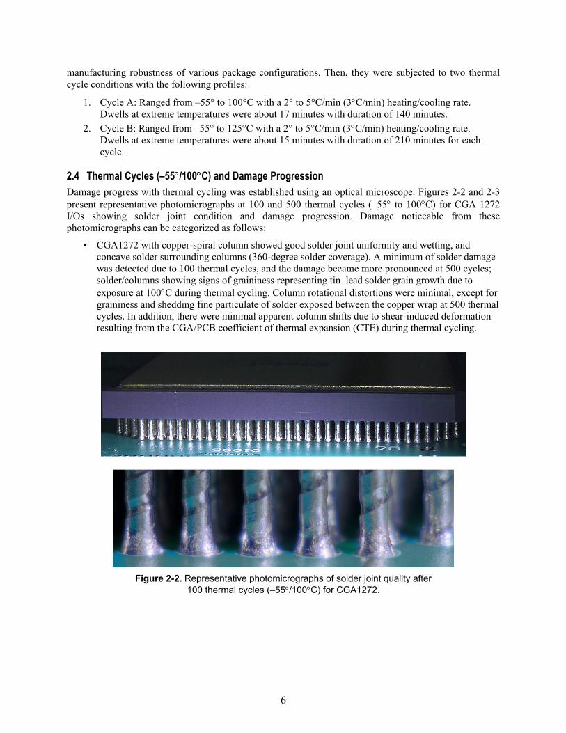
2.4 Thermal Cycles (–55/100C) and Damage Progression Damage progress with thermal cycling was established using an optical microscope. Figures 2-2 and 2-3 present representative photomicrographs at 100 and 500 thermal cycles (–55 to 100C) for CGA 1272 I/Os showing solder joint condition and damage progression. Damage noticeable from these photomicrographs can be categorized as follows:
• CGA1272 with copper-spiral column showed good solder joint uniformity and wetting, and concave solder surrounding columns (360-degree solder coverage). A minimum of solder damage was detected due to 100 thermal cycles, and the damage became more pronounced at 500 cycles; solder/columns showing signs of graininess representing tin–lead solder grain growth due to exposure at 100C during thermal cycling. Column rotational distortions were minimal, except for graininess and shedding fine particulate of solder exposed between the copper wrap at 500 thermal cycles. In addition, there were minimal apparent column shifts due to shear-induced deformation resulting from the CGA/PCB coefficient of thermal expansion (CTE) during thermal cycling.
Figure 2-2. Representative photomicrographs of solder joint quality after
100 thermal cycles (–55/100C) for CGA1272.
7
Figure 2-3. Representative photomicrographs of solder joint quality after 500 thermal cycles (–55/100C) for CGA1272.
2.5 Thermal Cycles (–55/125C) and Damage Progression Visual inspection was performed to establish damage progression of the outer columns of CGAs at thermal cycling intervals by optical microscopy. Figure 2-4 presents representative photomicrographs at 500 thermal cycles (–55 to 125C) for CGA 1272 I/Os showing solder joint condition and damage progression. Damage due to thermal cycling, noticeable from these photomicrographs, can be summarized as follows:
• CGA1272 with copper spiral columns showed good solder joint uniformity and wetting after assembly.
• However, some solder damage is apparent at 500 cycles; they show noticeable signs of graininess and particulate shedding of solder within copper wrap, which is representative of tin–lead solder grain growth due to long exposure at 125C during thermal cycling and local CTE mismatches.
• Column rotational distortion is low, even with such high signs of graininess. • There are no apparent column shifts due to thermal cycling.
So, similarly to thermal cycle condition A (–55 to 100C), less deformation occurred for CGA1272 with lower package dimension and higher rigidity of columns than those of CGA1752 both factors induce lower thermal stress on solder joint attachment.
8
Figure 2-4. Representative photomicrographs of solder joint quality after 500 thermal cycles (–55/125C) for CGA1272.
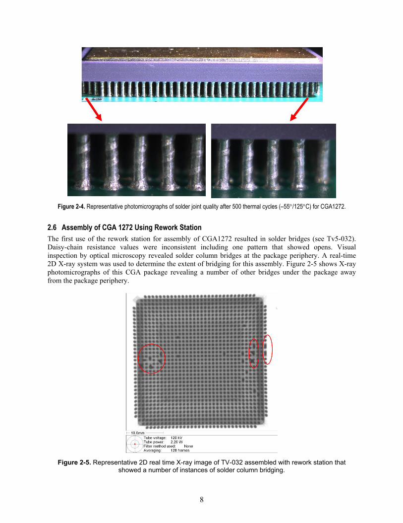
2.6 Assembly of CGA 1272 Using Rework Station The first use of the rework station for assembly of CGA1272 resulted in solder bridges (see Tv5-032). Daisy-chain resistance values were inconsistent including one pattern that showed opens. Visual inspection by optical microscopy revealed solder column bridges at the package periphery. A real-time 2D X-ray system was used to determine the extent of bridging for this assembly. Figure 2-5 shows X-ray photomicrographs of this CGA package revealing a number of other bridges under the package away from the package periphery.
Figure 2-5. Representative 2D real time X-ray image of TV-032 assembled with rework station that showed a number of instances of solder column bridging.
9
One reason for column bridging is thought to be the size of nozzle employed being the same as the package; this did not allow an effective flow of hot air during the reflow process. For a subsequent reflow, a new nozzle was designed that was slightly larger than the package size. Also, the reflow process was modified by increasing maximum temperature and dwell time. The new process parameters were implemented for assembly of another CGA1272 on the PCB using a previously designed mini stencil for solder paste printing. Use of the new process and the rework station again resulted in a solder column bridge even though we were successful in removing the peripheral solder bridges (see Figure 2-6).
Figure 2-6. Optical photomicrographs of CGA1272 assembled with the rework station after assembly and after removal of peripheral solder column bridges.
The above process was repeated using a new CGA1272 package; however, this time the solder paste behavior during reflow was monitored visually. The rework process had to be aborted two times just before solder reflow because of solder paste spreading during the initial heating process. After careful review of the process steps, the cause of solder paste spreading was identified. This enabled us to achieve an acceptable assembly process for CGA1272 assembly using the rework station. As apparent from Figure 2-7, a real time 2D X-ray revealed no solder column bridging. Even though the effect of such a process on behavior under thermal cycling is yet to be characterized as, “assembled,” test vehicles are considered to be acceptable. Further verification is required regarding the repeatability of this process.
10
Figure 2-7. Representative of 2D real time X-ray of a CGA 1272 I/O assembled with rework station that showed no solder column bridging.
11
3.0 CGA TEST DATA FOR LGAS WITH ADDED COLUMNS
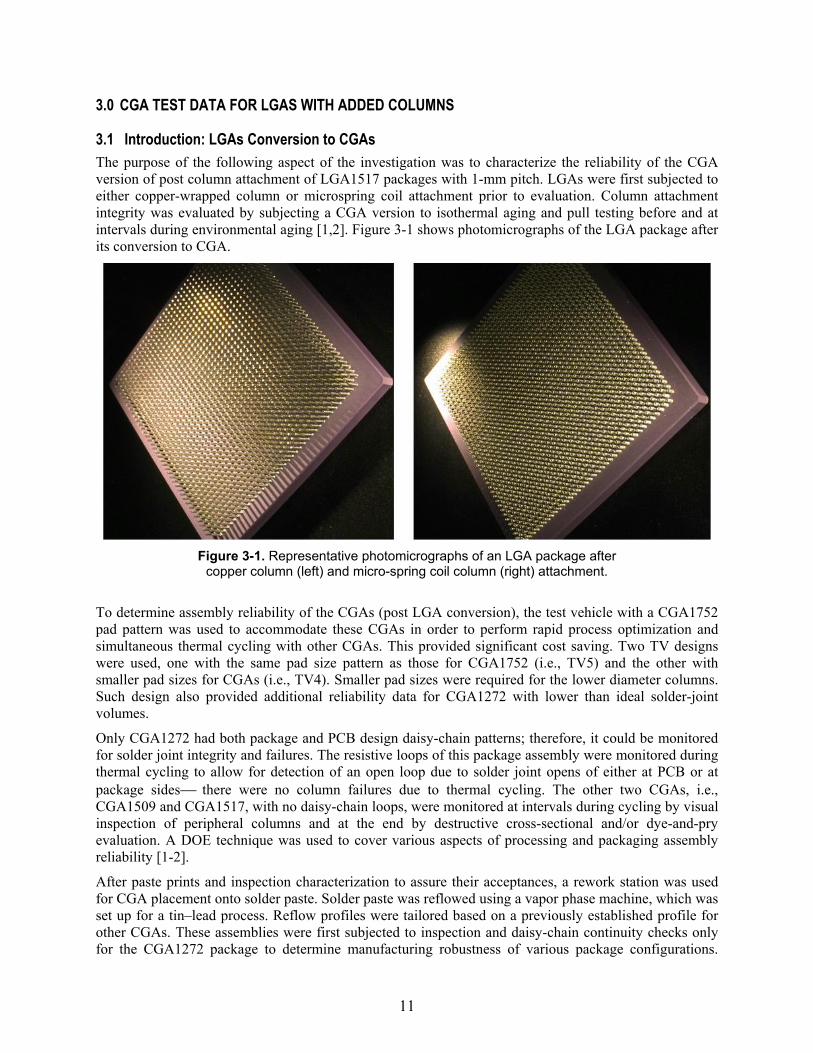
3.1 Introduction: LGAs Conversion to CGAs The purpose of the following aspect of the investigation was to characterize the reliability of the CGA version of post column attachment of LGA1517 packages with 1-mm pitch. LGAs were first subjected to either copper-wrapped column or microspring coil attachment prior to evaluation. Column attachment integrity was evaluated by subjecting a CGA version to isothermal aging and pull testing before and at intervals during environmental aging [1,2]. Figure 3-1 shows photomicrographs of the LGA package after its conversion to CGA.
Figure 3-1. Representative photomicrographs of an LGA package after
copper column (left) and micro-spring coil column (right) attachment.
To determine assembly reliability of the CGAs (post LGA conversion), the test vehicle with a CGA1752 pad pattern was used to accommodate these CGAs in order to perform rapid process optimization and simultaneous thermal cycling with other CGAs. This provided significant cost saving. Two TV designs were used, one with the same pad size pattern as those for CGA1752 (i.e., TV5) and the other with smaller pad sizes for CGAs (i.e., TV4). Smaller pad sizes were required for the lower diameter columns. Such design also provided additional reliability data for CGA1272 with lower than ideal solder-joint volumes.
Only CGA1272 had both package and PCB design daisy-chain patterns; therefore, it could be monitored for solder joint integrity and failures. The resistive loops of this package assembly were monitored during thermal cycling to allow for detection of an open loop due to solder joint opens of either at PCB or at package sides there were no column failures due to thermal cycling. The other two CGAs, i.e., CGA1509 and CGA1517, with no daisy-chain loops, were monitored at intervals during cycling by visual inspection of peripheral columns and at the end by destructive cross-sectional and/or dye-and-pry evaluation. A DOE technique was used to cover various aspects of processing and packaging assembly reliability [1-2].
After paste prints and inspection characterization to assure their acceptances, a rework station was used for CGA placement onto solder paste. Solder paste was reflowed using a vapor phase machine, which was set up for a tin–lead process. Reflow profiles were tailored based on a previously established profile for other CGAs. These assemblies were first subjected to inspection and daisy-chain continuity checks only for the CGA1272 package to determine manufacturing robustness of various package configurations.
12
Visual inspection of peripheral columns was performed for all assemblies since the board was designed with the intention of visual characterization. Furthermore, only two CGAs were assembled on each PCB to avoid blocking for visual inspection. Only outer rows (and in some cases, second and third rows) could be assessed for solder joint quality. The visual inspection particularly was critical for the mechanical CGAs with no daisy-chain patterns. Reliability was evaluated by exposing the CGAs to a number of environmental conditions and by subjecting them to nondestructive and destructive failure analyses techniques to characterize their failure mechanisms. This section also presents failure analyses evaluations.
3.2 Thermal Cycle Test Results
3.2.1 Thermal Cycle Test Results (55/100C) Table 3-1 presents a summary of assembly condition of CGA1509, CGA1517, and daisy-chain resistance values for CGA1272s after being mounted onto PCBs. The letters A, B, and C shown in Table 3-1 represent daisy-chain patterns from sets of outer rows to inner rows, respectively. Conditions of assemblies are presented in the column 2 of the table describing details on the board design types (TV4 or TV5), paste types (type 4 or type 5), CGA types (1509, 1517, 1272), column types (solid or copper-spiral column), and daisy-chain values for CGA1272 assemblies (3 loops) as assembled and after thermal cycling (–55°C to 100°C). These assemblies were subjected to condition A cycling, ranging from –55°C to 100°C with a 3°C/min heating/cooling rate and dwells at the extreme temperatures were 17 minutes with durations of 140 minutes.
The criteria for an open solder joint specified in IPC-9701 [11] were used as guidelines to interpret electrical interruptions. Opens were verified manually at convenient cycling intervals, but also at 100 and 200 thermal cycles. Measurements were performed at room temperature (RT) for CGA1272 that had a daisy-chain configuration, and this allowed comparison of resistance values prior to thermal cycling to identify opens. Even though a number of assemblies were near failure based on visual inspection, the resistance values after 100 to 500 cycles indicated no failures. The TV5-032 failed after assembly build due to using the rework station for assembly a significantly more challenging process rather than a more robust vapor phase reflow. The key DOE parameters, including process variables, are summarized in column 2 of the table.
For CGA 1272, in addition to loop resistance monitoring, visual inspection was also performed by optical microscopy to establish damage progression of outer columns assemblies at thermal cycle intervals. For CGA 1509 and 1517 I/Os, only visual inspection at intervals was performed.
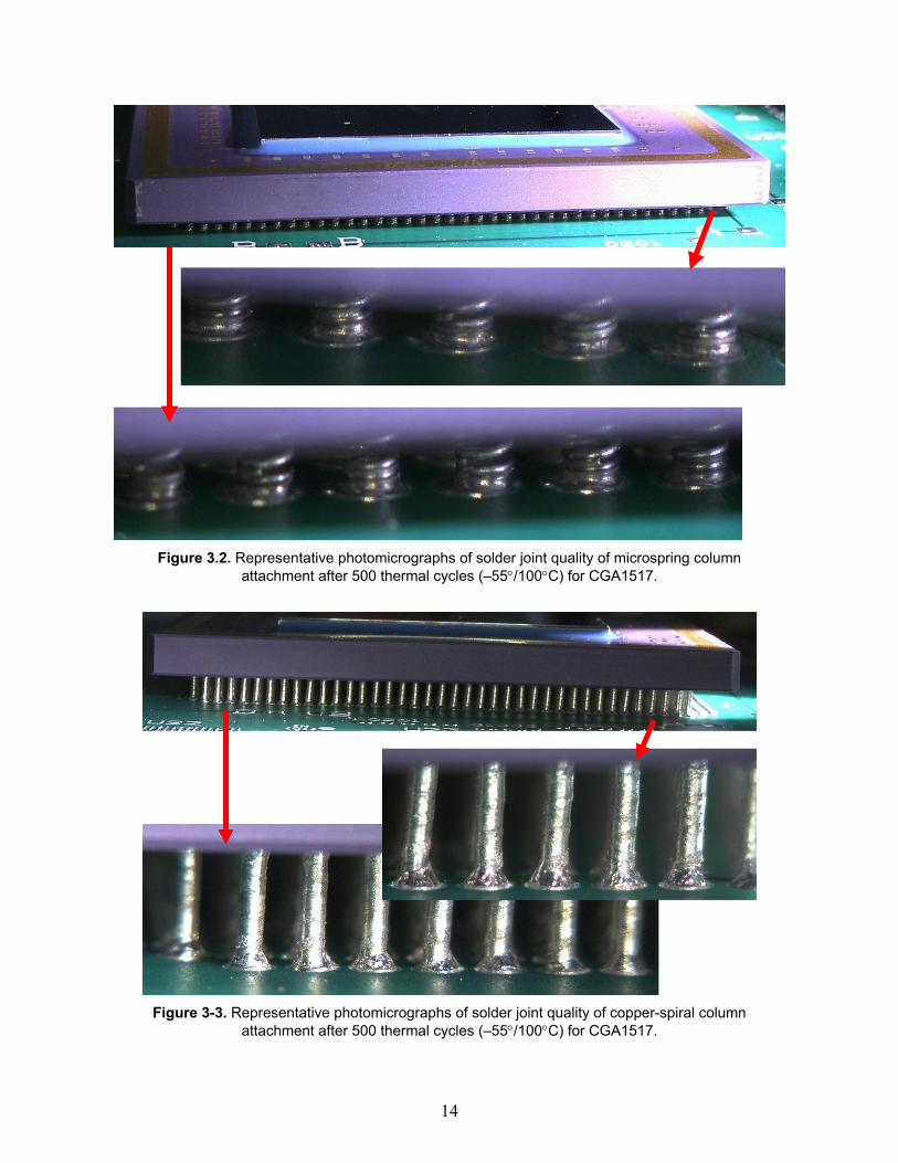
Figures 3-2 and 3-3 present representative photomicrographs of solder joint condition of two CGA 1517 I/Os, one with microspring and the other with copper-wrapped columns, respectively. Damage appears to be minor for both cases due to 500 thermal cycles (55C to 100C). Only slight dullness indicates some damage due to cycling, and there are no signs of microcracks.
13
Table 3-1. Summary of daisy-chain resistance measurements (in ohms) within each CGA package, after assembly and thermal cycles (–55/100C) at 100 to 500 cycles.
3.2.2 Thermal Cycle Test Results (55/125C) Table 3-2 presents a summary of assembly conditions of CGA1509 and CGA1517, and daisy-chain resistance values for CGA1272. In this case, the test vehicles were subjected to thermal cycling ranging from –55°C to 125°C with a 3°C/min heating/cooling rate. The resistance values after 100 to 500 cycles indicate no failures, except the TV4-023 and TV4-024. Both assemblies lacked ideal pad design; therefore, the “low” had low solder volume. In addition, TV5-024 had an added intentional defect in the solder paste of the corner solder columns. This assembly showed one daisy-chain loop open after assembly.
ID Paste Type & Process CGA A-CGA1272 B-CGA1272 C-CGA1272
TV5-011Type5 Tin-Lead Paste, Vapor Phase, CGA1517 MicroSpring and CGA1272 DC CGA1517 1.89 2.49 2.15
100 Cycles (-55 C to 100 C) NA 1.99 2.57 2.49
200 Cycles (-55 C to 100 C) NA 1.96 2.57 2.53
300 Cycles (-55 C to 100 C) NA 2.01 2.61 2.62
400 Cycles (-55 C to 100 C) NA 1.98 2.60 2.67500 Cycles (-55 C to 100 C)
NA2.00 2.61 2.71
TV5-014Type4 Tin-Lead Paste, Vapor Phase, CGA1517 MicroSpring and CGA1272 DC CGA1517 1.85 2.42 2.04
100 Cycles (-55 C to 100 C) NA 1.91 2.5 2.11
200 Cycles (-55 C to 100 C) NA 1.91 2.5 2.12
300 Cycles (-55 C to 100 C) NA 1.91 2.49 2.11
400 Cycles (-55 C to 100 C) NA 1.94 2.51 2.13500 Cycles (-55 C to 100 C)
NA1.96 2.54 2.15
TV5-017Type4 Tin-Lead Paste, Vapor Phase/Stencil 5, CGA1517 Cu Column and CGA1272 DC CGA1517 2.05 2.63 2.22
100 Cycles (-55 C to 100 C) NA 1.9 2.48 2.11
200 Cycles (-55 C to 100 C) NA 1.87 2.45 2.1
300 Cycles (-55 C to 100 C) NA 1.90 2.48 2.12
400 Cycles (-55 C to 100 C) NA 1.88 2.47 2.10500 Cycles (-55 C to 100 C)
NA1.93 2.51 2.14
TV4-021Type5 Tin-Lead Paste, Vapor Phase, CGA1517 Cu Column and No CGA1272 DC CGA1517 NP NP NP
100 Cycles (-55 C to 100 C) NA NP NP NP
200 Cycles (-55 C to 100 C) NA NP NP NP
300 Cycles (-55 C to 100 C) NA NP NP NP
400 Cycles (-55 C to 100 C) NA NP NP NP500 Cycles (-55 C to 100 C)
NANP NP NP
TV5-032
Type5 Tin-Lead Paste, Vapor Phase, CGA1509 90/10 Column and CGA1272 Rework Station CGA1517 1.67 open 0.43
100 Cycles (-55 C to 100 C) NA 1.7 open 0.46
200 Cycles (-55 C to 100 C) NA 1.73 open 0.47450 Cycles (-55 C to 100 C)
NA1.74 open 0.47
14
Figure 3.2. Representative photomicrographs of solder joint quality of microspring column
attachment after 500 thermal cycles (–55/100C) for CGA1517.
Figure 3-3. Representative photomicrographs of solder joint quality of copper-spiral column attachment after 500 thermal cycles (–55/100C) for CGA1517.
15
Table 3-2. Summary of daisy-chain resistance measurements (in ohms) within each CGA package, after assembly and thermal cycles (–55/125C) at 100 to 500 cycles.
300 Cycles (-55 C to 100 C) NP NP NP
400 Cycles (-55 C to 100 C) NP NP NP500 Cycles (-55 C to 100 C) NP NP NP
TV5-032
Type5 Tin-Lead Paste, Vapor Phase, CGA1509 90/10 Column and CGA1272 Rework Station 1509 1.67 open 0.43
100 Cycles (-55 C to 100 C) 1.7 open 0.46
200 Cycles (-55 C to 100 C) 1.73 open 0.47450 Cycles (-55 C to 100 C) 1.74 open 0.47
ID Paste Type & Process CGA A-1272 B-1272 C-1272
TV5-012Type4 Tin-Lead Paste, Vapor Phase, CGA1517 MicroSpring and CGA1272 DC 1517 1.88 2.48 2.1
100 Cycles (-55 C to 125 C) 1.95 2.57 2.18
200 Cycles (-55 C to 125 C) 1.92 2.53 2.15
300 Cycles (-55 C to 125 C) 1.94 2.55 2.16
400 Cycles (-55 C to 125 C) 1.98 2.62 2.21500 Cycles (-55 C to 125 C) 1.96 2.58 2.19
TV5-013Type4 Tin-Lead Paste, Vapor Phase, CGA1517 MicroSpring and CGA1272 DC 1517 1.87 2.45 2.09
100 Cycles (-55 C to 125 C) 1.92 2.53 2.17
200 Cycles (-55 C to 125 C) 1.91 2.52 2.15
300 Cycles (-55 C to 125 C) 1.94 2.53 2.17
400 Cycles (-55 C to 125 C) 1.98 2.58 2.21500 Cycles (-55 C to 125 C) 1.95 2.55 2.17
TV5-015
Type4 Tin-Lead Paste, Vapor Phase/Stencil 4, CGA1517 Cu Column and CGA1272 DC 1517 1.88 2.48 2.11
100 Cycles (-55 C to 125 C) 1.97 2.57 2.19
200 Cycles (-55 C to 125 C) 1.97 2.55 2.19
300 Cycles (-55 C to 125 C) 1.96 2.56 2.20
400 Cycles (-55 C to 125 C) 2.00 2.62 2.23500 Cycles (-55 C to 125 C) 1.99 2.60 2.23
TV5-016
Type4 Tin-Lead Paste, Vapor Phase/Stencil 5, CGA1517 Cu Column and No CGA1272 DC 1517 1.86 2.45 2.07
100 Cycles (-55 C to 125 C) 1.9 2.51 2.14
200 Cycles (-55 C to 125 C) 1.89 2.51 2.13
300 Cycles (-55 C to 125 C) 1.93 2.54 2.15
400 Cycles (-55 C to 125 C) 1.94 2.54 2.16500 Cycles (-55 C to 125 C) 1.92 2.53 2.14
TV4-022
Type4 Tin-Lead Paste/Stencil4, Vapor Phase, CGA1517 Cu Column and CGA1272 DC 1517 1.94 2.53 2.11
100 Cycles (-55 C to 125 C) 1.98 2.57 2.18
200 Cycles (-55 C to 125 C) 1.98 2.57 2.16
300 Cycles (-55 C to 125 C) 2.02 2.63 2.20
400 Cycles (-55 C to 125 C) 1.99 2.60 2.17500 Cycles (-55 C to 125 C) 2.06 2.67 2.22
TV4-023
Type4 Tin-Lead Paste/Stencil4, Vapor Phase, CGA1517 Cu Column and CGA1272 DC-Induced Ink Defect at Assembly 1517 1.98 2.57 2.16
100 Cycles (-55 C to 125 C) 2.05 2.65 2.23
200 Cycles (-55 C to 125 C) 2.02 2.63 2.21
300 Cycles (-55 C to 125 C) 2.05 2.65 2.23
400 Cycles (-55 C to 125 C) 2.08 2.69 2.25500 Cycles (-55 C to 125 C) 2.05 3.57 2.23
TV4-024
Phase, CGA1517 Cu Column and CGA1272 DC-Induced Kapton Defect at Assembly 1517 Open 2.54 2.11
100 Cycles (-55 C to 125 C) Open 2.62 2.19
200 Cycles (-55 C to 125 C) Open 2.61 2.19
300 Cycles (-55 C to 125 C) open 2.63 2.20
400 Cycles (-55 C to 125 C) Open 2.65 2.21500 Cycles (-55 C to 125 C) Open 2.66 2.20
TV5-031
Type4 Tin-Lead Paste, Vapor Phase, CGA1509 90/10 Column and CGA1272 DC 1509 1.92 2.52 2.14
100 Cycles (-55 C to 125 C) 1.95 2.54 2.17
200 Cycles (-55 C to 125 C) 2 2.59 2.21
300 Cycles (-55 C to 125 C) 2.00 2.59 2.21
400 Cycles (-55 C to 125 C) 1.95 2.53 2.17
16
In addition to daisy-chain monitoring for CGA1272, visual inspection by optical microscopy was also performed for all CGAs to establish damage progression of the outer columns. Figures 3-4 and 3-5 present representative photomicrographs of solder joint condition for CGA 1517 with microspring and copper-wrapped columns after 500 thermal cycles (55C to 125C). A slightly darker appearance of solder joints at the PCB side of the microspring column attachments indicates a slight sign of damage due to 500 thermal cycling.
Figure 3-4. Representative photomicrographs of solder joint quality of microspring column
attachment after 500 thermal cycles (–55/125C) for CGA1517.
17
Figure 3-5. Representative photomicrographs of solder joint quality of copper-spiral column attachment after 500 thermal cycles (–55/125C) for CGA1517.
18
4.0 FAILURE ANALYSIS FOR CGA 1752, 1517, AND 1272 I/O
4.1 Overview: Inspection Methods (Visual, Daisy Chain, and Dye-and-Pry) Two monitoring approaches were used to determine integrity of CGA solder joints during thermal cycling. Visual inspection by optical microscopy was performed for all assemblies, but daisy-chain monitoring for resistance open was made only for those assemblies that had a daisy-chain pattern after assembly. The CGA1517 had no daisy chain; therefore, it could not be monitored electrically for an open. Failure analysis by cross-sectioning and dye-and-pry (dye-n-pry) was performed to further narrow levels of damage progression and cracking of solder joints. Even though failure analysis by cross-sectioning in conjunction with scanning electron microscopy provide excellent details on solder joint behavior; they are however not only an expensive pair of processes, but they are limited in scope of detection—one thin row of columns at a time.
Dye-and-pry failure analysis is another valuable approach that is simple and provides an insight into the whole area of package column attachment. In this approach, an assembly is penetrated with a liquid color dye, then the package is pried upward. Ideally, separation occurs at the weakest link and the interfaces also reveal failures of the solder joints if the solder joints happened to be the weakest link. If the interfaces have not weakened enough, then, pull loading will cause breakage of the package substrate or stretch the columns. Then, it is possible that full separation may not occur to easily enable the failure characterization. Nevertheless, valuable information is still gathered from the failure of the peripheral columns due to prying. This section presents failure analyses and mechanisms for CGAs.
4.2 Failure Analysis of CGA 1752 and BME Capacitors (TV5)
CGA1752 with BME capacitors on the ceramic substrates after thermal cycling (–55 to 125C) and vibration-to-failure were subjected to failure analyses. The assembly was cut in half; one-half for dye-and-pry and the other half for cross-sectioning evaluation. Figure 4-1 shows photomicrographs of red-dyed assembly before and after prying; it shows complete separation of the assembly into halvespackage and PCB and failure mechanisms. The total number of columns in the section was 1034 sites, in which 38 pulled through the PCB pad lifting (cratering), about 3.7%. Since there was no stain on the lifted pad, the pad lifts were considered to be due to prying, not cratering due to thermal cycling or vibration. The other noticeable failure mechanism was a half-cone solder cavity on the PCB pads. The cavity represents the condition of solder fillet after reflow, with only partial solder fillet formation on the PCB pads. Asymmetrical solder fillet with a slight degree of tilt is the norm for the pure solder column and is acceptable for yield and reliability. It is postulated that during prying, columns were first pulled apart from the no-fillet section, and then solder was deformed during the last stage of separation and stretched to form a half-cup solder left on the PCB pads. The majority of the separated sites from the PCB pads, only 113 sites (11.3%), were from the package pads.
Figure 4-2 shows the BME capacitors before and after dye-and-pry showing stained red substrate and the package pads. Areas of red dye are apparent on all pads; however, no full red coverage of the pads was observed. Lack of full red stain indicates that there was no solder joint full failure of the BMEs despite the number of thermal cycles. Partial failures are apparent.
19
Figure 4-1. Representative dye-and-pry photomicrographs of failures at assembly before pry (top), at PCB (bottom-left), and at package (bottom-right) sites after pry for CGA1752 after cycling
(–55/125C).
Figure 4-2. Representative dye-and-pry photomicrographs of failures BME capacitors on CGA1752 substrate before pry at assembly (top) and after pry (bottom) after cycling (–55/125C).
20
Although, dye-and-pry provided details on the failure sites and mechanisms for the column and for the BME capacitor attachments; however, it did not reveal the condition of the flip-chip die, which also have critical interconnections. Die with wire bond rather than flip-chip die were the interconnections of the choice for the previous package generations. Wire bond reliability is well established and is robust. This is not the case for the flip-chip die within CGA, which is a newer technology with a lesser-known reliability establishment. Cross sectioning of the package through the die could reveal the integrity of the flip-chip die attachment as well as column to package and PCB. Because of the existence of soft and hard materials, it is difficult to polish a large part such as CGA1752.
Figure 4-3 shows optical photomicrographs taken at a lower magnification in order to reveal the location of polishing (near the center of the package) and the overall package configuration. It includes the optical photomicrographs of the flip-chip die and column solder joints at a higher magnification. For reference, a scanning electron microscopy (SEM) image of the corner flip-chip bump is also included in the figure. There was no evidence of cracking of solder bumps in those scanned optically and by SEM. However, partial cracking of the corner columns are apparent from the magnified image. Note that the edge columns at the center section of a package assembly generally were exposed to lower stresses due to the CTE mismatches compared to the corner columns of CGA package with the largest distance to neutral point (DNP). Hence, the corner columns were exposed higher stresses and developed more severe cracks.
Figure 4-3. Representative optical and SEM cross-sectional photomicrographs of CGA1752 showing damage of solder joint on PCB and integrity of the flip-chip die within package after cycling (–55/125C).
4.3 Failure Analysis of CGA1272 on Small Pad (TV4-022) Two different PCBs were used one with the standard (i.e., test vehicle serial number 5, TV5) and the other with smaller pad diameters (TV4). The TV4 pad design could accommodate the smaller diameter of 15-mil (0.381-mm) columns of copper spiral and microspring of CGA1517 I/O. Ideally, a 20-mil (0.508-mm) diameter column is a better choice because of added column rigidity. However, the manufacturer of the column attachment would not guarantee the integrity of attachments if we decided to enforce the use of a 20-mil (0.508-mm) diameter column. So, we chose the 15-mil (0.381-mm) column diameter. With this choice, the smaller pad size became non-ideal for CGA 1272 with the 20-mil columns. The PCB pad size of about 20 mil (0.508-mm) then became the same as the 20 mil (0.508-mm) column diameter no space for solder fillets and lower solder volume. A number of TV4s had both CGA 1517 and CGA 1272 packages; therefore, the CGA 1272 resulted in having smaller solder volume with no solder fillet. The TV4-022 through TV-023 had this condition for CGA 1272. The TV-022 vehicle was the control unit. Figure 4-4 shows a photomicrograph of this test vehicle after 300 thermal cycles (–55/125C); clearly shows the lack of solder fillet condition. For theses test vehicles, because of the low solder volumes and
21
lack of solder joint fillets, the solder joints showed signs of microcracks and failed much earlier than the test vehicle built under a standard condition (TV5).
Figure 4-4. Representative photomicrographs of solder joint quality of copper-spiral column attachment after 300 thermal cycles (–55/125C) for TV4-CGA1272 with pad the same size as solder
column diameter.
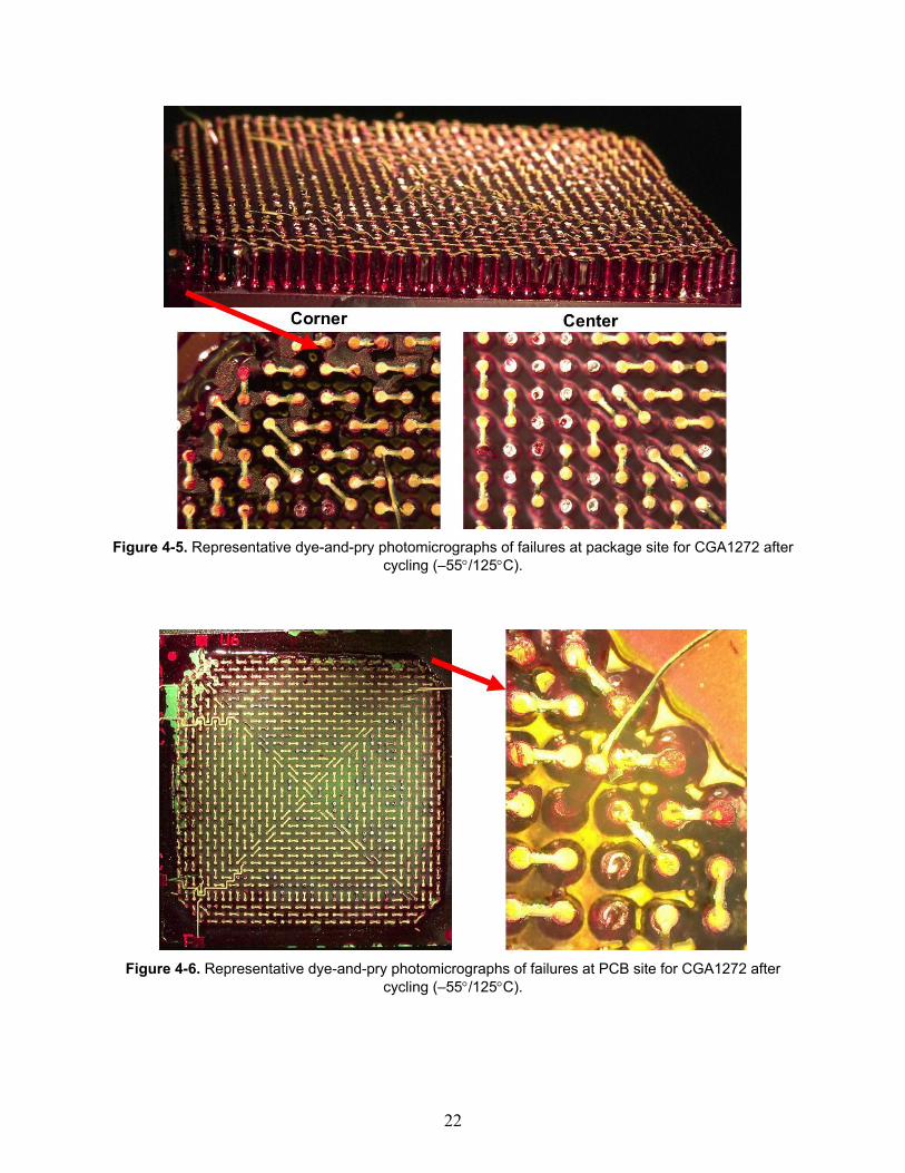
After early failure detection by daisy chain, the assembly was subjected to red dye first and then was pried for failure location detection. Figures 4-5 and 4-6 compare the failure mechanisms at the package and at the PCB sites. More than 96% of failures were due to pad cratering and lift. It appears that integrity of pad adhesion might have been compromised with such a pad configuration. Full red stains on the pad lift in the corner pads confirm early failure occurrence due to the lack of solder fillet.
22
Figure 4-5. Representative dye-and-pry photomicrographs of failures at package site for CGA1272 after cycling (–55/125C).
Figure 4-6. Representative dye-and-pry photomicrographs of failures at PCB site for CGA1272 after cycling (–55/125C).
23
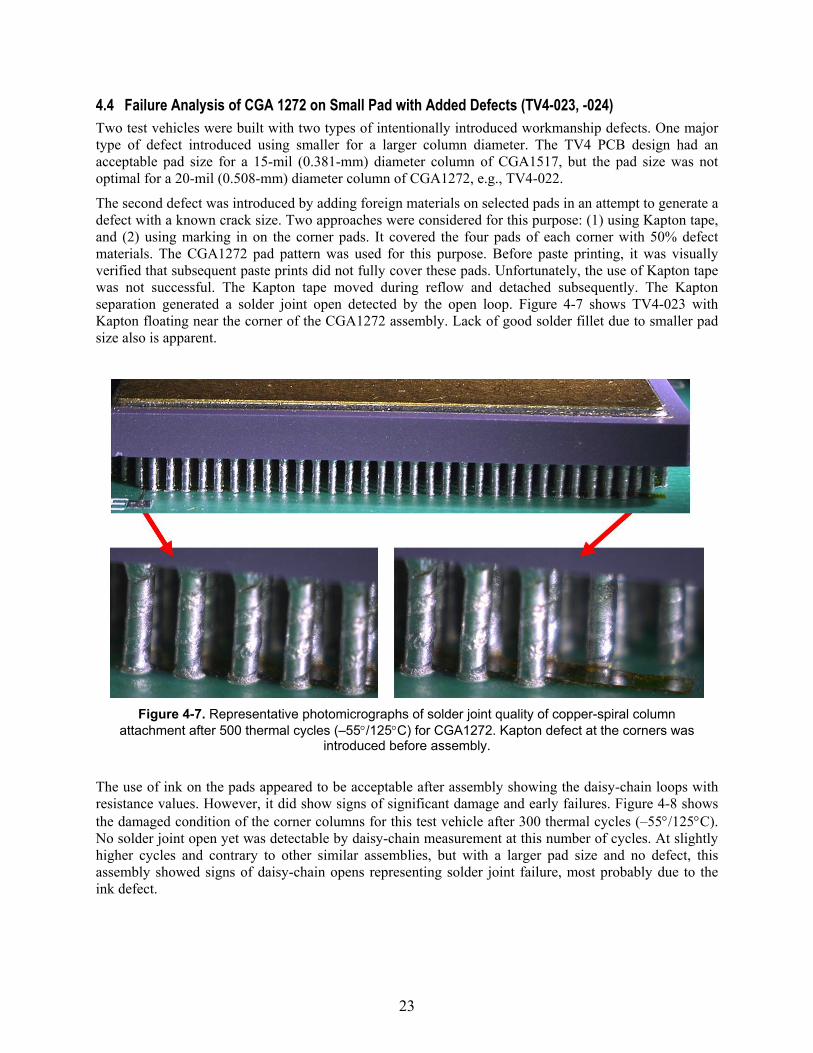
4.4 Failure Analysis of CGA 1272 on Small Pad with Added Defects (TV4-023, -024) Two test vehicles were built with two types of intentionally introduced workmanship defects. One major type of defect introduced using smaller for a larger column diameter. The TV4 PCB design had an acceptable pad size for a 15-mil (0.381-mm) diameter column of CGA1517, but the pad size was not optimal for a 20-mil (0.508-mm) diameter column of CGA1272, e.g., TV4-022.
The second defect was introduced by adding foreign materials on selected pads in an attempt to generate a defect with a known crack size. Two approaches were considered for this purpose: (1) using Kapton tape, and (2) using marking in on the corner pads. It covered the four pads of each corner with 50% defect materials. The CGA1272 pad pattern was used for this purpose. Before paste printing, it was visually verified that subsequent paste prints did not fully cover these pads. Unfortunately, the use of Kapton tape was not successful. The Kapton tape moved during reflow and detached subsequently. The Kapton separation generated a solder joint open detected by the open loop. Figure 4-7 shows TV4-023 with Kapton floating near the corner of the CGA1272 assembly. Lack of good solder fillet due to smaller pad size also is apparent.
Figure 4-7. Representative photomicrographs of solder joint quality of copper-spiral column attachment after 500 thermal cycles (–55/125C) for CGA1272. Kapton defect at the corners was
introduced before assembly.
The use of ink on the pads appeared to be acceptable after assembly showing the daisy-chain loops with resistance values. However, it did show signs of significant damage and early failures. Figure 4-8 shows the damaged condition of the corner columns for this test vehicle after 300 thermal cycles (–55/125C). No solder joint open yet was detectable by daisy-chain measurement at this number of cycles. At slightly higher cycles and contrary to other similar assemblies, but with a larger pad size and no defect, this assembly showed signs of daisy-chain opens representing solder joint failure, most probably due to the ink defect.
24
Figure 4-8. Representative photomicrographs of solder joint quality of copper-spiral column attachment after 300 thermal cycles (–55/125C) for CGA1272. The ink defect at the corners was
introduced before assembly.
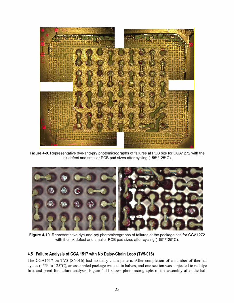
After failure of this assembly, the dye-and-pry technique was used to verify failure mechanism due to the ink defect and smaller pad size. Figure 4-9 shows photomicrographs of the PCB pad pattern after full separation due to prying. Photomicrographs of the four corners and an enlarged pattern pads are included in the photos. As expected, stain covered corner pads indicate a failure condition from the PCB pads. This however, was not the case for the most of the other pads, even though copper pad separation from the PCB was dominant. The package pad sites showed a lower number of separations (see Figure 4-10). The white reflections at the separated package represent pad separation during thermal cycling. The failures from either package or PCB sites clearly show competing failure mechanisms; in which for this case, failure becomes dominant at the PCB sites. The ink defect and smaller pad sizes favored failure at the PCB sites.
25
Figure 4-9. Representative dye-and-pry photomicrographs of failures at PCB site for CGA1272 with the ink defect and smaller PCB pad sizes after cycling (–55/125C).
Figure 4-10. Representative dye-and-pry photomicrographs of failures at the package site for CGA1272 with the ink defect and smaller PCB pad sizes after cycling (–55/125C).
4.5 Failure Analysis of CGA 1517 with No Daisy-Chain Loop (TV5-016) The CGA1517 on TV5 (SN016) had no daisy-chain pattern. After completion of a number of thermal cycles (–55 to 125C), an assembled package was cut in halves, and one section was subjected to red dye first and pried for failure analysis. Figure 4-11 shows photomicrographs of the assembly after the half
26
sample was subjected to prying, but in this case, it was not fully separated. The top photo shows an overall image of package stained showing lack of full separation. Column distortion with copper wrap twist or failure is apparent. The middle photo is a higher magnification of the top photo with focus on the failure modes at the PCB interfaces. It shows no apparent failure of the solder joints yet. The bottom photo concentrates on the package solder joint interface failure. Again, there are no apparent failures of solder joints at the interfaces.
Figure 4-11. Representative dye-and-pry photomicrographs of failures at PCB site for CGA1517 after cycling (–55/125C).
The other half of the sample was cross-sectioned to verify dye-and-pry failure observations as well as a solder bump condition within the flip-chip die. Although, in this case, dye-and-pry provided limited details on failure mechanisms; nevertheless, in any case, it did not reveal the condition of the flip-chip die, which also have critical interconnections. Careful cross sectioning of the package through the die should reveal the integrity of the flip-chip die attachment (see Figure 4-12) as well as solder joints conditions at the package and at the PCB levels. There were no anomalies for the solder joint of the flip-chip die, but this was not the case for the column solder joint attachments. The optical photomicrographs of the copper-wrapped columns at higher magnifications (see Figure 4-13), particularly those at the row
27
edges, showed signs of microcracking. These columns had lower thermal stresses than package corner columns; therefore, corner columns are expected to show much higher degree of microcracking.
Figure 4-12. Representative optical cross-sectional photomicrographs of CGA1517 showing minimum signs of damage for the flip-chip solder joints within package after cycling (–55/125C).
Figure 4-13. Representative cross-sectional optical photomicrographs of CGA1517 showing microcracking after cycling (–55/125C).
28
4.6 Failure Analysis of CGA 1517 with No Daisy-Chain Loop (TV4-023) A CGA1517 was assembled on the TV4 test vehicle with a smaller pad also subjected to dye-and-pry for comparison to those of TV5. This package had no daisy-chain pattern; therefore, only failure analysis reveals actual failure even though inspection of peripheral columns provides some insight into solder damage and progression. Figure 4-14 shows photomicrographs after prying the TV4-023 assembly sample and having a number of thermal cycles (–55 to 125C). Both PCB and package sites are shown in the figure. Separations of pads are apparent from the both photos, especially the package pad sites. All columns remaining on the packages either separated by the pad lifting or by solder joint failures.
Figure 4-14. Representative dye-and-pry photomicrographs of failures at PCB and Package sites for CGA1517 (TV4-023) after cycling (–55/125C).
29
5.0 CHALLENGES OF DIRECT LGA ASSEMBLY ONTO PCB
5.1 Overview: Why LGA onto PCB This section covers direct attachment of ceramic land grid array packages onto PCBs to understand generic issues associated with LGA solder joint assembly. For high reliability applications, this approach may become a popular approach with a much wider implementation of restriction of hazardous substances (ROHS). It may became even a more significant consideration for evaluation for aerospace applications since a recent announcement by a major manufacturer of FPGA CGA packages that it will supply packages only in the CN (LGA) configuration. However, LGAs in plastic package versions with much smaller sizes have been available for thinner consumer products because of lower cost and lower assembly standoff compared to ball-grid-array versions. In some cases, the LGAs are optimized in improving radio frequency (RF) performance for wireless applications.
For example, a high coefficient of thermal expansion (HCTE) ceramic LGA has been recently introduced replacing HCTE ball grid arrays (BGA) packages. The LGA solder interconnect is formed solely by solder paste applied at the board assembly because there are no spheres attached to the LGA. It was reported that for HCTE LGAs [10], a lower standoff height could be achieved of approximately 0.06-mm to 0.1-mm, depending on solder paste volume and PCB geometry. The pad surface finish of LGA is generally electroless gold plating, 0.1 to 0.5 μm, over electroless nickel. The LGAs with such surface finish become ROHS compliant.
Key features of an LGA packages include:
• LGA packages eliminate risk of damaged columns or spheres due to shipping or handling.
• LGA packages are ROHS compliant and can be used for either lead-containing or lead-free assemblies.
• LGA packages have a lower mounted height than CGA/BGA; this can allow for more space above the device for a heat-sink solution or for small form-factor applications.
• HCTE LGA lead-free solder paste is reported to have a better board-level reliability than ceramic ball grid array (CBGA) versions with tin–lead.
• LGAs in general have much lower board-level reliability. The reduction on reliability is yet to be established.
Before establishing the board-level reliability, the LGA manufacturing parameters need to be optimized. The purpose of the following aspects of the investigation was to determine the direct assembly challenge of an LGA1517 and LGA1272 package with 1-mm pitch where both large size and heavy weight of the package are of great concern. In a previous section, it was shown that LGAs could be successfully converted into CGAs by either attachment of copper-wrapped or microspring-coiled columns. These CGAs were then assembled onto PCBs, and they successfully passed a number of thermal cycles with no failures. For LGAs, assembly processes for larger LGAs in either plastic or ceramic version are yet to be established. This section will address direct assembly of LGAs onto PCBs.
5.2 LGA 1517 Assembly For smaller and lighter LGAs, the simplest process is to print solder paste, place the package onto the paste, and subject it to a reflow process. This process may not be expanded for a larger plastic LGA with an adequate corner warpage causing potential solder joint opens as well as a heavy ceramic LGA with weight sufficient to squeeze out solder paste causing solder bridging. For the heavy LGA1517 package, in order to avoid solder bridging, the part was subjected to tin–lead solder paste printing first and then was reflowed to form solder domes on their pads. Initial solder domes provided some rigidity and control on
30
solder height; it also increased its standoff. The solder dome formation for the LGA1517 process was successful and generated uniform solder bumps with no bridging (see Figure 5-1).
Figure 5-1. Ceramic land grid array (LGA) package as received (top) and with solder bumps generated
by SnPb paste print and reflow (bottom).
The next step was to assemble an LGA package with newly formed solder bumps onto a PCB. Even with solder bumps on the pads, collapse of the package during assembly still was of concern. Additional spacing controls were added on the periphery of the LGA package in order to control the height of assembly. After paste print and placement of the LGA by a rework station, the assembly was reflowed using the process developed for CGA1517. Because of a lower height, visual inspection did not reveal the condition of the peripheral solder joints; it commonly could be evaluated for CGAs. The LGA assembly was subject to a 2D X-ray for detecting quality of assembly, solder balls, and bridging. Figure 5-2 shows an overall X-ray photomicrograph of the LGA assembly. Quality of the solder joints appears to be acceptable, and only one solder bridge was detected. The magnified image the solder bridge is also shown in the figure.
31
Figure 5-2. X-ray photomicrographs of assembled ceramic land grid array (LGA) package
showing quality of assembly and expanded view of one solder short.
To further verify condition of the assembly and reserve the LGA package, the assembly was subjected to removal using a rework station. Several attempts allowed removal of the LGA package such that most solder bumps remained on the LGA package. The aim was to verify quality of assembly by preserving the integrity of the solder and possibly the bridge; but this goal could not be achieved because of solder melting and distortion during removal procedure. The next step was to clean the solder from the LGA pads, use a new PCB, repeat these processes, and include lessons learned from the first trial.
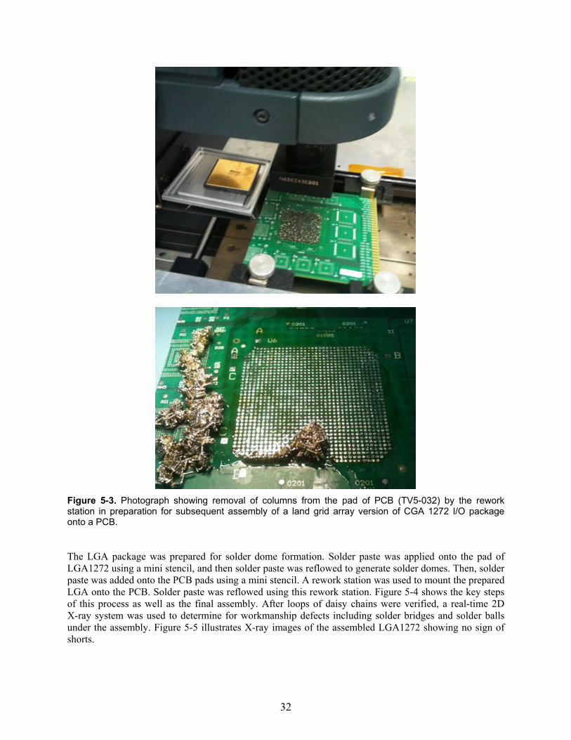
5.3 LGA1272 Assembly Using Rework Station The trial for the LGA1272 assembly was accomplished first by reworking an assembled CGA1272, which had solder bridges (see Tv5-032), and then re-assembling it as an LGA package. After rework of CGA1272 for package removal, both the package and the PCB sites were prepared for subsequent re-assembly (see Figure 5-3). Most of the columns remained on the PCB site. Site dressing is required to remove any remaining columns, to correct the solder composition or completely remove the high-lead residue from the original eutectic solder joints, and to improve the planarity to the pads. The high-lead residue has an elevated reflow temperature. If it is not removed, the residue may impede the reflow and self-centering of the replacement module.
32
Figure 5-3. Photograph showing removal of columns from the pad of PCB (TV5-032) by the rework station in preparation for subsequent assembly of a land grid array version of CGA 1272 I/O package onto a PCB.
The LGA package was prepared for solder dome formation. Solder paste was applied onto the pad of LGA1272 using a mini stencil, and then solder paste was reflowed to generate solder domes. Then, solder paste was added onto the PCB pads using a mini stencil. A rework station was used to mount the prepared LGA onto the PCB. Solder paste was reflowed using this rework station. Figure 5-4 shows the key steps of this process as well as the final assembly. After loops of daisy chains were verified, a real-time 2D X-ray system was used to determine for workmanship defects including solder bridges and solder balls under the assembly. Figure 5-5 illustrates X-ray images of the assembled LGA1272 showing no sign of shorts.
33
Figure 5-4. Series of photographs showing replacement of CGA with LGA 1272 I/O of TV5-032. It shows solder paste print on PCB, solder bumping on LGA1272, Kapton tape stand-off and reflow by nozzle, and final assembly.
Figure 5-5. X-ray photomicrographs of assembled ceramic land grid array (LGA) package (Originally TV-032, CGA) showing no signs of solder shorts.
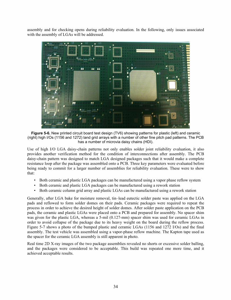
5.4 Plastic and Ceramic LGA Assemblies on HDI PCB To determine manufacturing challenges of LGAs and the effects of other packaging parameters; a new printed circuit board was designed to accommodate both high I/O ceramic and plastic LGA packages. The ceramic LGA had 1272 lands whereas the plastic version had 1156 lands (see Figure 5-6). This board had a number of additional new features including new surface finish and microvia-in-pad for package daisy-chain routing. Other packages with finer pitches were also designed to better understand assembly issues with finer pitch as well. All packages (including LGAs) had daisy-chain patterns for checking opens after
34
assembly and for checking opens during reliability evaluation. In the following, only issues associated with the assembly of LGAs will be addressed.
Figure 5-6. New printed circuit board test design (TV6) showing patterns for plastic (left) and ceramic (right) high I/Os (1156 and 1272) land grid arrays with a number of other fine pitch pad patterns. The PCB
has a number of microvia daisy chains (HDI).
Use of high I/O LGA daisy-chain patterns not only enables solder joint reliability evaluation, it also provides another verification method for the condition of interconnections after assembly. The PCB daisy-chain pattern was designed to match LGA designed packages such that it would make a complete resistance loop after the package was assembled onto a PCB. Three key parameters were evaluated before being ready to commit for a larger number of assemblies for reliability evaluation. These were to show that:
• Both ceramic and plastic LGA packages can be manufactured using a vapor phase reflow system • Both ceramic and plastic LGA packages can be manufactured using a rework station • Both ceramic column grid array and plastic LGAs can be manufactured using a rework station
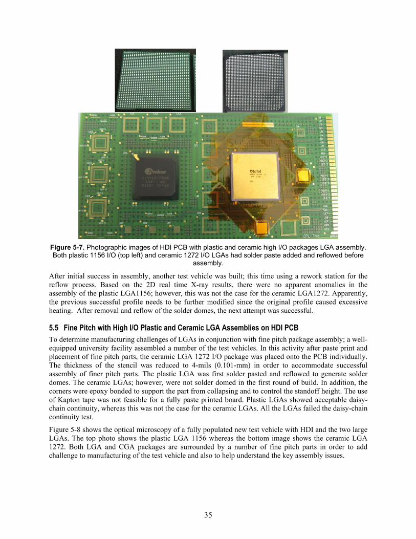
Generally, after LGA bake for moisture removal, tin–lead eutectic solder paste was applied on the LGA pads and reflowed to form solder domes on their pads. Ceramic packages were required to repeat the process in order to achieve the desired height of solder domes. After solder paste application on the PCB pads, the ceramic and plastic LGAs were placed onto a PCB and prepared for assembly. No spacer shim was given for the plastic LGA, whereas a 5-mil (0.127-mm) spacer shim was used for ceramic LGAs in order to avoid collapse of the package due to its heavy weight on the board during the reflow process. Figure 5-7 shows a photo of the bumped plastic and ceramic LGAs (1156 and 1272 I/Os) and the final assembly. The test vehicle was assembled using a vapor-phase reflow machine. The Kapton tape used as the spacer for the ceramic LGA assembly is still apparent in photo.
Real time 2D X-ray images of the two package assemblies revealed no shorts or excessive solder balling, and the packages were considered to be acceptable. This build was repeated one more time, and it achieved acceptable results.
35
Figure 5-7. Photographic images of HDI PCB with plastic and ceramic high I/O packages LGA assembly. Both plastic 1156 I/O (top left) and ceramic 1272 I/O LGAs had solder paste added and reflowed before
assembly.
After initial success in assembly, another test vehicle was built; this time using a rework station for the reflow process. Based on the 2D real time X-ray results, there were no apparent anomalies in the assembly of the plastic LGA1156; however, this was not the case for the ceramic LGA1272. Apparently, the previous successful profile needs to be further modified since the original profile caused excessive heating. After removal and reflow of the solder domes, the next attempt was successful.
5.5 Fine Pitch with High I/O Plastic and Ceramic LGA Assemblies on HDI PCB To determine manufacturing challenges of LGAs in conjunction with fine pitch package assembly; a well-equipped university facility assembled a number of the test vehicles. In this activity after paste print and placement of fine pitch parts, the ceramic LGA 1272 I/O package was placed onto the PCB individually. The thickness of the stencil was reduced to 4-mils (0.101-mm) in order to accommodate successful assembly of finer pitch parts. The plastic LGA was first solder pasted and reflowed to generate solder domes. The ceramic LGAs; however, were not solder domed in the first round of build. In addition, the corners were epoxy bonded to support the part from collapsing and to control the standoff height. The use of Kapton tape was not feasible for a fully paste printed board. Plastic LGAs showed acceptable daisy-chain continuity, whereas this was not the case for the ceramic LGAs. All the LGAs failed the daisy-chain continuity test.
Figure 5-8 shows the optical microscopy of a fully populated new test vehicle with HDI and the two large LGAs. The top photo shows the plastic LGA 1156 whereas the bottom image shows the ceramic LGA 1272. Both LGA and CGA packages are surrounded by a number of fine pitch parts in order to add challenge to manufacturing of the test vehicle and also to help understand the key assembly issues.
36
Figure 5.8. New test vehicle design (TV6) showing two half images. The top photo shows fine pitch parts surrounding the large plastic LGA 1156 I/O, and the bottom image shows the ceramic LGA 1272 I/O packages surrounded by other fine pitch packages. The PCB has a number of microvia daisy chains
(HDI) including large plastic and ceramic LGAs.
The overall X-ray of the two sides similar to the optical photomicrographs is shown in Figure 5-9. It shows also the corner solder joints at a higher X-ray magnification for the two large LGAs. The X-ray images show the internal configuration of the LGAs and the fine pitch packages. During real time review of the X-ray images at higher magnifications, unusual solder anomalies were apparent for the ceramic LGA1272, but not for the plastic LGA1156. The X-ray images of LGA1272 showed a solder grainy/lumpy appearance with numerous condition of partial solder coverage or shift on the pads (package and board). This demonstrated that a mix technology assembly with LGAs is challenging and needs further investigation.
To verify the X-ray observations, a ceramic LGA package was pried from the board. Figure 5-10 shows side-by-side the solder remains on the PCB and the LGA pad patterns. It clearly shows partial solder coverage of the LGA pads and solder graininess. Hence, the optical microscopy confirmed the X-ray observation.
37
Figure 5-9. X-ray photomicrographs of TV6 fully populated assembly. It includes both plastic LGA 1156 I/O (top) and ceramic LGA 1272 I/O (bottom) and X-rays of their corners at higher magnification. Solder
joint voids for the plastic LGA and defect anomalies for the ceramic LGA are apparent.
Figure 5-10. Optical photomicrograph of a ceramic LGA 1272 I/O showing optically apparent solder joint anomalies confirming the anomalies detected by X-ray.
38
6.0 KEY FINDINGS This final report (third in series) presented updates on thermal cycle testing for a number of CGAs, failure analyses by non-destructive and destructive methods, and characterization of LGA packages and assemblies on the PCB with microvia in the pad with associated processes and reliability. It updated the thermal cycling test matrix to include the recently gathered thermal cycle data to 500 thermal cycles for CGA packages and assemblies. The high input/output CGA test results included those with 1272, 1509, 1517, and 1752 I/Os; three column types (pure solder, copper-wrapped, and microspring); and 1-mm pitch. The thermal cycles ranged from a low temperature of 55C to maximum temperatures of either 100C or 125C with a slow ramp up rate of 3C/min and dwell times of about 15 minutes at the two temperature extremes. Photomicrograph images were presented to delineate key optical microscopy inspection findings after up to 500 thermal cycles before destructive failure analyses. Extensive failure analyses were performed by the dye-and-pry technique to determine failure mechanismsseparation of pad either from package or PCB pads, solder joints, and column failures.
Dye-and-pry was performed for most assemblies, but it was specifically chosen for those assemblies with intentionally induced defects. These intentional defects were shown to cause significant degradation on the integrity of solder joints. Their negative effects were detected in some cases immediately after assembly and in other cases during early thermal cycling exposure. The induced defects included placement of CGAs with larger column diameters on smaller PCB pads and 50% coverage of four corner columns to initiate microcracking defects during manufacturing. Dye-and-pry failure analyses were performed for the CGA1517 I/O assemblies, which had no daisy-chain pattern. Microsectioning was also performed to validate dye-and-pry findings and especially to determine the integrity of the solder-bump joints for the flip-chip die within the package.
With the recent announcement that a key CGA package supplier is planning to move away from CGA supplying only the land grid array stylea new test vehicle was designed to address such a move. The objectives were: (1) to address conversion of LGA to CGAs and (2) to determine challenges of direct assembly of LGAs onto the PCB. The new PCB was designed to address the high I/O LGA issues both for plastic and ceramic versions as well as those included in a large number of finer pitch area array packages. Finer pitch package required that the PCB be designed with the high density interconnects (HDI), microvia. Standard PCB design with no microvias has been shown to be acceptable for the larger pitch LGAs. A few key processing approaches were considered to understand the issues associated with the direct LGA assembly onto the PCB prior to evaluating thermal cycle behavior of the HDI PCB. Because of difficulty of inspection by optical microscopy, X-ray was the key inspection approach for assuring quality of LGA assemblies. Key findings are presented for CGAs/LGAs assembled onto standard/HDI PCBs. Thermally cycled and destructively/non-destructively performed failure analyses are summarized in the following list.
• For LGAs, it was established that LGAs could be successfully converted into CGAs using two different column types: solder columns with copper wrapping or microspring coils with no solder columns. It was also shown that these converted CGA packages could be assembled successfully onto PCBs if the PCB pad design and other processing parameters were appropriately optimized for the type/size of package and column.
• For column attachment integrity, it was established behavior of copper-wrapped column solder joint attachment by the isothermal aging at 125C and pull testing the columns.
• For extremely larger CGA packages, it was shown that the large/thick CGAs with 1752 I/O solid solder column could be successfully assembled onto PCBs using three different solder paste types. Solder joint appearance for this style of column type is different from either copper-wrapped or microspring coil columns.
39
• For the BME capacitors, those mounted on the substrate of a non-hermetic CGA, it was shown that the capacitors could survive thermal shock-cycles as well as process reflow and subsequent thermal cycles.
• For the BME capacitors, it presented a comprehensive report on their solder joint workmanship defects.
• For accelerated thermal cycling (ATC), in general, the reliability of the solder column connection is driven by the CTE mismatch between the ceramic and the epoxy-glass PCB. The stresses in the joints are highest at the corners of the ceramic, which are at the greatest distance from the neutral point (DNP), hence, the effect of CGA size, materials, and configuration. These critical factors should be considered when comparing the ATC test results for various CGAs and performing failure analyses.
• For an ATC profile of 55/100C, CGA1272 with copper-spiral columns, they showed good solder joint uniformity and wetting, with concave solder surrounding columns. Minimum solder damage was detected after 100 thermal cycles, and that damage had increased by 500 cycles (55/100C); solder/columns showed signs of gross graininess representing tin–lead solder grain growth due to exposure at 100C during thermal cycling. Column shift and distortions were minimal, possibly due to stiffer copper wrap, at 500 thermal cycles. No apparent column shifts were apparent due to shear-induced deformation because of mismatch CTE of CGA and PCB.
• For an ATC profile of 55/125C, CGA1272 with copper-spiral column, they showed good solder joint uniformity and wetting. Definite solder damage was apparent at 500 cycles; it showed signs of significant graininess representing tin–lead solder grain growth due to exposure at 125C during thermal cycling. Column distortions were minimal.
• For ATC profile of 55/100C and 55/125C, CGA1752— larger than CGA1272 and with high-lead solid-solder columns — showed partial solder joint coverage of column perimeter with good wetting on the coverage area. Several displaced columns showing a larger corner column shift were apparent.
• For both ATC conditions (55/100C and 55/125C), it was observed that less deformation occurred for CGA1272 with smaller package dimension and higher rigidity of columnsboth factors cause lower thermal stresses on solder joint attachmentcompared to larger CGA1752 package and lower rigid pure solder columns.
• For both CGA 1752 and 1272 I/Os, it was shown that solder damage and microcracks induced, especially for CGA1752, were generally significantly higher for the 55/125C thermal cycle profile than those under the 55/100C cycling condition.
• For CGA1272 assembly onto standard PCB pad sizes, e.g. TV5, it was shown that about 96% failures were from the pad cratering under dye-and-pry pull testing after thermal cycling. Pad cratering is an issue that should be further investigated using bare board. For CGA1272 on smaller PCB pad sizes with intentionally induced defects at the corner columns, failure occurred by full separation of solder at defects with similar conditions of PCB pad cratering.
• For CGA 1517, there were two failure mechanisms observed due to dye-and-pry testing, one showed mostly column failures while the other mostly PCB pad separation. The reason for such a drastic difference in failures is yet to be determined.
• For CGA 1517 and 1752 I/Os, microsectioning revealed no solder joint failure of the flip-chip die solder bumps and joints.
• For direct ceramic LGA assembly, it was shown that ceramic the LGA 1517 package could be successfully solder paste printed and reflowed to form solder dome on the pads. X-ray detected one short after assembly onto the PCB.
40
• For LGAs direct assembly onto PCBs, numerous LGA1272s were assembled onto PCBs after being solder paste printed to form solder dome on package pad. The results were mixed with a limited success. The causes for such variations are yet to be determined.
• For plastic LGAs, it was demonstrated that high I/O plastic LGAs could be successfully assembled onto PCBs after solder dome formation on the package before assembly.
• For X-ray evaluation, it was demonstrated that the real-time 2D X-ray could only reveal the fully rejected condition of an LGA assembly, but not microcracks in solder joints. The condition was verified by mechanically separating the assembly and performing inspection by optical microscope. It is, however, difficult to detect cracks and opens within a sound assembly.
The qualification guidelines presented in this report, which are based on the test results for CGA/LGA/HDI packages and board assemblies, will facilitate NASA projects use of newly available and very dense FPGA area array packages with known reliability and mitigation risks, allowing greater processing power in a smaller board footprint and lower system weight.
41
7.0 ACRONYMS AND ABBREVIATIONS
ATC accelerated thermal cycling 3D three dimensional BGA ball grid array BME base metal electrode CBGA ceramic ball grid array CCGA ceramic column grid array CGA column grid array COTS commercial-off-the-shelf CQFP ceramic quad flat pack CSP chip scale (size) package CTE coefficient of thermal expansion Cu copper DNP distance to neutral point DOE design of experiment EDX/EDS energy dispersive x-ray FPGA field programmable gate array FCBGA flip-chip ball grid array HASL hot-air solder leveling HCTE high coefficient of thermal expansion HDI high density interconnect I/O input/output JPL Jet Propulsion Laboratory LGA land grid array MIP mandatory inspection point NASA National Aeronautics and Space Administration NEPP NASA Electronic Parts and Packaging PBGA plastic ball grid array PCB printed circuit board PME precious metal electrode PWB printed wiring board QA quality assurance QFP quad flat pack RF Radio frequency ROHS restriction of hazardous substances RT Room temperature SEM scanning electron microscopy SMT surface mount Tg glass transition temperature TV test vehicle
42
8.0 REFERENCES [1] Ghaffarian, R., “Reliability of CGA/LGA/HDI Package Board/Assembly, Rev. A” Interim report, NEPP
report, NASA Goddard Space Flight Center, Greenbelt, MD, Jan. 2013. https://nepp.nasa.gov/ [2] Ghaffarian, R., “Reliability of CGA/LGA/HDI Package Board/Assembly,” Interim report, NEPP report,
NASA Goddard Space Flight Center, Greenbelt, MD, Jan. 2012. https://nepp.nasa.gov/ [3] Ghaffarian, R., “Damage and Failures of CGA/BGA Assemblies under Thermal Cycling and Dynamic
Loadings,” ASME 2013 International Mechanical Engineering Congress and Engineering. IMECE2013, November 15-21, San Diego, California, USA.
[4] Ghaffarian, R., “Thermal Cycle and Vibration/Drop Reliability of Area Array Package Assemblies,” Chapter 22 in Structural Dynamics of Electronics and Photonic Systems, eds. E. Suhir, E. Connally, and D. Steinberg Springer, 2011.
[5] Ghaffarian, R., “Thermal Cycle Reliability and Failure Mechanisms of CCGA and PBGA Assemblies with and without Corner Staking,” IEEE Transactions on Components and Packaging Technologies, June 2008, vol. 31, issue 2.
[6] Ghaffarian, R., “Area Array Technology for High Reliability Applications,” Chapter 16 in Micro-and Opto-Electronic Materials and Structures: Physics, Mechanics, Design, Reliability, Packaging, ed. E. Suhir , Springer, 2006.
[7] Ghaffarian, R., “CCGA Packages for Space Applications,” Microelectronics Reliability, Vol. 46, pp. 2006–2024, 2006.
[8] Ghaffarian, R., “BGA Assembly Reliability,” Chapter 20 in Area Array Packaging Handbook, ed. K. Gilleo, McGraw-Hill, 2004.
[9] Fjelstad, J., Ghaffarian, R., and Kim, Y.G., “Chip Scale Packaging for Modern Electronics,” Electrochemical Publications, vol. 20, no. 4, p. 47, 2002.