Silicon back contact solar cell configuration: A pathway towards higher efficiency M.K. Mat Desa a,b,n , S. Sapeai a , A.W. Azhari a,c , K. Sopian a , M.Y. Sulaiman a , N. Amin a , S.H. Zaidi a a Solar Energy Research Institute, National University of Malaysia, 43600 Bangi, Selangor, Malaysia b School of Electrical & Electronic Engineering, USM Engineering Campus, 14300 Nibong Tebal, Pulau Pinang, Malaysia c School of Environmental Engineering, Universiti Malaysia Perlis, 01000 Kangar, Perlis, Malaysia article info Article history: Received 11 August 2014 Received in revised form 3 January 2016 Accepted 2 March 2016 Available online 24 March 2016 Keywords: Silicon solar cells Screen-printed solar cells Nanostructures Emitter wrap-through Metal-warp through Laser drilling Interdigitated back-contact abstract The back-contact crystalline silicon solar cell represents an advanced configuration in which inter- digitated positive and negative contacts are placed on the rear surface. Highest conversion efficiency, elimination of shading losses, co-planarity of cell interconnections, and uniform black appearance, represent some of the most significant features of this type of solar cell. However, the manufacturing process complexity leads to significantly higher production cost making it difficult to compete with conventional mono and poly crystalline Si-based Photovoltaics industry. Over the years, an increasing number of researchers have reported on methods and processes aimed at reduction in manufacturing cost. This review paper attempt an extensive review of several categories of back-contact silicon solar cells, relevant design innovations, specific cost advantages especially in terms of using lower lifetime materials, their efficiency advantages in terms of geometry and wafer type, and their manufacturing technologies. In addition, available simulation tools for numerical investigation on back-contact struc- tures and advanced device concepts have also presented in order to better understand underlying physical considerations in terms of passivation, both surface and volume, and minority carrier lifetime. & 2016 Elsevier Ltd. All rights reserved. Contents 1. Introduction ....................................................................................................... 1517 1.1. Silicon solar cell ............................................................................................... 1517 1.2. Silicon based back contact solar cell ............................................................................... 1517 2. Classification of back-contact solar cells ................................................................................. 1518 2.1. Metallization wrap through ..................................................................................... 1518 2.2. Emitter wrap through ......................................................................................... 1520 2.3. Interdigitated back contact ..................................................................................... 1520 2.4. Advanced back junction solar cell................................................................................ 1521 2.4.1. IBC Heterojunction..................................................................................... 1521 2.4.2. Microstructure IBC ..................................................................................... 1522 2.4.3. Bifacial nature of IBC ................................................................................... 1523 3. A review on fabrication process: starting materials........................................................................ 1523 3.1. Types of silicon wafers ........................................................................................ 1523 3.2. N-type vs. p-type wafer selection issue ........................................................................... 1523 3.3. Wafer lifetime, substrate doping and thickness issue ................................................................ 1524 4. Device fabrication issue.............................................................................................. 1524 4.1. Defining the emitter and base doping region ...................................................................... 1524 4.1.1. Photolithography based process .......................................................................... 1524 4.1.2. Pre-diffusion approach ................................................................................. 1525 Contents lists available at ScienceDirect journal homepage: www.elsevier.com/locate/rser Renewable and Sustainable Energy Reviews http://dx.doi.org/10.1016/j.rser.2016.03.004 1364-0321/& 2016 Elsevier Ltd. All rights reserved. n Corresponding author. E-mail address: [email protected](M.K. Mat Desa). Renewable and Sustainable Energy Reviews 60 (2016) 1516–1532
Transcript
Renewable and Sustainable Energy Reviews 60 (2016) 1516–1532
Contents lists available at ScienceDirect
Renewable and Sustainable Energy Reviews
http://d1364-03
n CorrE-m
journal homepage: www.elsevier.com/locate/rser
Silicon back contact solar cell configuration: A pathway towardshigher efficiency
M.K. Mat Desa a,b,n, S. Sapeai a, A.W. Azhari a,c, K. Sopian a, M.Y. Sulaiman a, N. Amin a,S.H. Zaidi a
a Solar Energy Research Institute, National University of Malaysia, 43600 Bangi, Selangor, Malaysiab School of Electrical & Electronic Engineering, USM Engineering Campus, 14300 Nibong Tebal, Pulau Pinang, Malaysiac School of Environmental Engineering, Universiti Malaysia Perlis, 01000 Kangar, Perlis, Malaysia
a r t i c l e i n f o
Article history:Received 11 August 2014Received in revised form3 January 2016Accepted 2 March 2016Available online 24 March 2016
Keywords:Silicon solar cellsScreen-printed solar cellsNanostructuresEmitter wrap-throughMetal-warp throughLaser drillingInterdigitated back-contact
x.doi.org/10.1016/j.rser.2016.03.00421/& 2016 Elsevier Ltd. All rights reserved.
The back-contact crystalline silicon solar cell represents an advanced configuration in which inter-digitated positive and negative contacts are placed on the rear surface. Highest conversion efficiency,elimination of shading losses, co-planarity of cell interconnections, and uniform black appearance,represent some of the most significant features of this type of solar cell. However, the manufacturingprocess complexity leads to significantly higher production cost making it difficult to compete withconventional mono and poly crystalline Si-based Photovoltaics industry. Over the years, an increasingnumber of researchers have reported on methods and processes aimed at reduction in manufacturingcost. This review paper attempt an extensive review of several categories of back-contact silicon solarcells, relevant design innovations, specific cost advantages especially in terms of using lower lifetimematerials, their efficiency advantages in terms of geometry and wafer type, and their manufacturingtechnologies. In addition, available simulation tools for numerical investigation on back-contact struc-tures and advanced device concepts have also presented in order to better understand underlyingphysical considerations in terms of passivation, both surface and volume, and minority carrier lifetime.
The sustainable development of renewable energy resources tomeet growing energy requirements is perhaps, the most criticalchallenge of the 21st century. At present, principal energyresources originate from carbon-based fossil fuels. At the currentfossil fuel usage rate, it is estimated that coal, gas, and oil will bedepleted in 107, 35, and 35 years, respectively [1]. Therefore,alternative renewable energy sources must be developed to meetescalating human energy requirements. One of most renownedrenewable energy technologies is photovoltaic technology. Fromeveryday items, such as digital watches, calculators, small portablechargers to rooftop and terrestrial applications, the technology isconstantly evolving, and becoming more prevalent in oureveryday lives.
Photovoltaic devices convert sunlight into electricity, with noheat, mechanical energy, noise, or by-products being releasedduring the conversion process. While the initial investment isquite high, the photovoltaic technology has attracted muchattention due to elegant energy conversion, reliability, and infiniteabundance of light energy. Initially, the photovoltaic technologywas specifically developed to generate power in space and extra-terrestrial applications, due to low conversion efficiency and highdevice cost [2]. At present, photovoltaic technology has become onpar with, or an even better economic alternative, than its fossilfuels counterpart. In the Netherland and several other developcountries, the cost of PV-based energy generation has alreadyreached parity with fossil-fuel based energy resources [3,4].
Photovoltaic technology can be classified according to the typeof material and the fabrication technology. General information onPhotovoltaic technology can be found in [5,6], while more detailedliterature, such as [7,8], covers specific types of photovoltaictechnology in greater detail. This paper focuses on an in-depthreview of an advanced silicon-based PV device, known as the back-contact solar cell, where recent advancements and future direc-tions of the technology are presented.
1.1. Silicon solar cell
Photovoltaic devices can generally be categorized as siliconbased, thin film (group III–V, group II–VI, group I–III–VI), organic,and advanced nano-PV [9–11]. The silicon-based photovoltaictechnology consists of mono and multi-crystalline solar cells thatremain the dominant market players, and is expected to lead themarket for the next several decades [10,12,13]. The silicon pho-tovoltaic is being favored, due to the abundance of the silicon rawmaterial and the silicon feedstock, robust fabrication technology,long operating life cycles, and high conversion efficiency [14].
According to Shockley and Quaser, the theoretical efficiency limitof a single junction silicon solar cell is about 29%. Despite this,
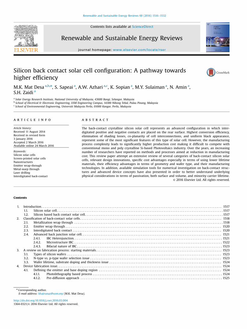
commercialized silicon solar cells, which are mainly screen-printedsilicon solar cells, have a much lower average efficiency, between 14%and 17%. The main loss mechanism is through the intrinsic losses ofsilicon material bandgap. Higher-energy photons of the sunlight areconverted into lattice vibrations (phonons), while low-energy pho-tons, below the bandgap, are unable to generate electron-hole pairs.Other losses are due to light reflection from the front surface, sha-dowing losses of front contact grids, resistive losses of metal contacts,and recombination losses of minority carriers within the bulk andthe surface regions [15]. Fig. 1 shows the structure of screen-printedcommercially available silicon-based solar cells. They consist of a p-type grade feedstock silicon wafer, a phosphorus-diffused emitter, analkaline texturing front surface, a screen-printed silver contact(front), and an aluminum back-surface field (BSF) [16].
The method use to the reduce cost in screen-printed solar cellsis to use thinner and larger-size wafers [14,18]. As a result, thewafer thickness has been reduced from 630 μm to 200 μm, with aprojected further reduction to 160 μm in 2015 [19]. The diameterof the wafer used has also been expanded from 4" to 8". However,this strategy has its fundamental limitations due to wafer bowingcaused by the thermal expansion mismatch between the alumi-num and the silicon [20]. Moreover, thinner and larger wafers aremore vulnerable to cracks during wafering, wet-chemical proces-sing, high temperature diffusion, screen printing, and the rapidthermal annealing process. All of these factors contribute to pooroutput yield.
Another limitation associated with the use of thinner and lar-ger wafers, is the tradeoff between series resistance and the sha-dowing losses of the front contact grid. The front contact grid mustbe designed as small as possible, to reduce the shadowing losseswhile still maintaining good conductivity [18]. In larger wafers,significantly high current passes through the front metal grid,which increases the resistive losses. This problem worsens whensolar cells are wired by contact tabs, causing a slight drop in effi-ciency when making a panel [21].
One way to solve the problems mentioned above is through theformation of both positive and negative contacts on the backplaneof the solar cell. This solar cell configuration is known as the back-contact solar cell. Back-contact solar cells eliminate shadow lossesand restrictions on metal-contact/busbar dimensions, since thepositive and the negative contacts are located on the backplane.
1.2. Silicon based back contact solar cell
Silicon-based back-contact solar cells have advantages of zeroshading losses and low contact resistance. Module fabrication hasbecome simpler due to co-planar cell interconnection. In addition,panels have become more attractive due to their uniform darkappearance and higher packing density. However, strict materialquality requirements and complex fabrication methods are the
M.K. Mat Desa et al. / Renewable and Sustainable Energy Reviews 60 (2016) 1516–15321518
challenges that must be addressed before back-contact solarstructure can fully be adopted in silicon solar-cell industry.
With zero shading loss, all of the incident light can reach thefront surface of the solar cell. Therefore, back-contact structure cangenerate a higher photogenerated current. This leads to higherefficiency, compared to a conventional silicon solar cell. The back-contact solar cell structure is one of the few solar cell designs thatachieve more than twenty-percent efficiency. Other solar celltypes are the PERL, the HIT, and the multifunction solar cell [22–24]. More info can be obtained in Table 1. In addition, the rear-contact design structure allows bigger and wider contacts to beused since it does not face the sun. This tackles one of the mainissues in silicon solar cell design, known as resistive loss. Fur-thermore, the absence of a front contact grid makes the-back-contact solar cells suitable for concentrating application.
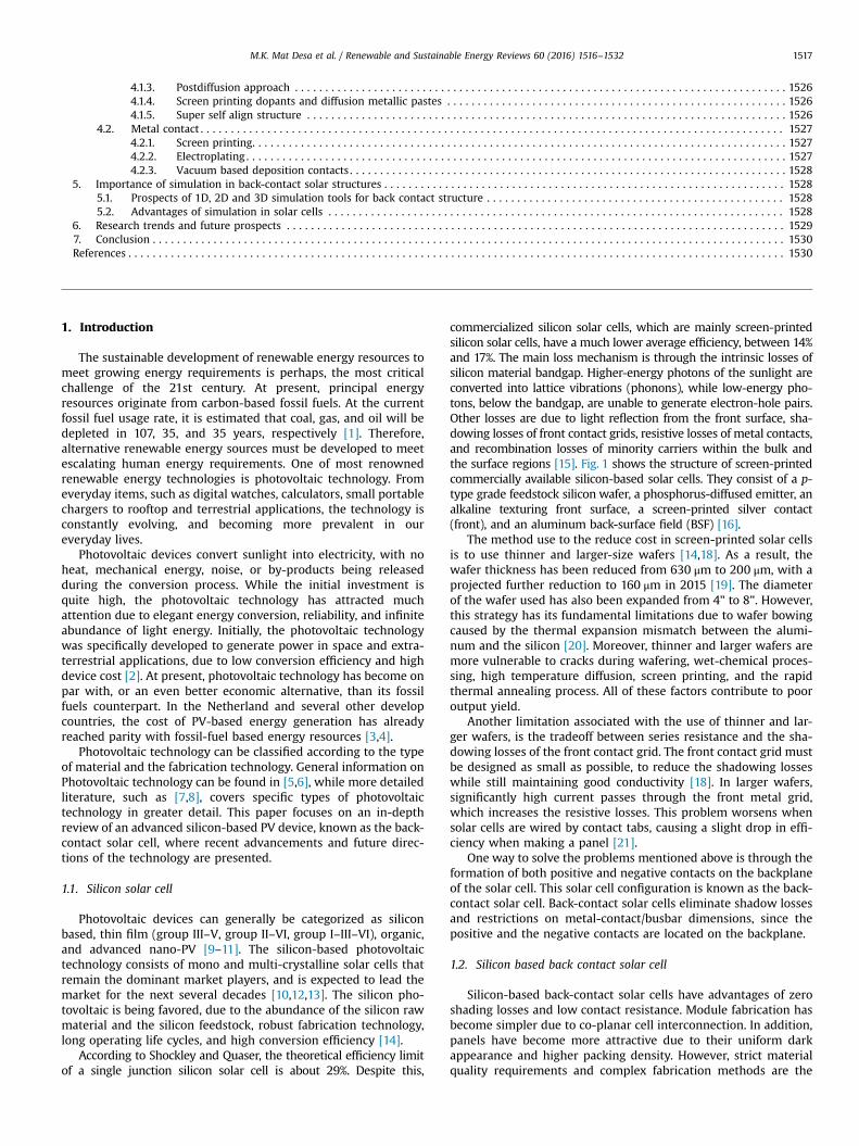
Other notable advantages of back-contact structures can befound during module fabrication. The back-contact structureallows single plane interconnection, as shown in Fig. 2. This co-planar cell interconnection simplifies the module fabrication
P-type
Al Back Contact
Front Contact (Ag)
Textured Front Surface
N+ (phosphorous)
p+ back surface field
Fig. 1. Schematic of commercially available screen printed silicon solar cell struc-ture [17].
Table 1The highest PV devices conversion efficiency of according to the types measure at AM
process, allowing for thinner and larger wafers to be used, even-tually reduces the module manufacturing costs [25,26]. Largetabbing wires can also be used for cell interconnection, leading tomore reliable interconnection, reducing conduction losses, andimproving the fill factor of the module. As a result, there is asmaller efficiency gap when converting cells into modules, com-pared to a conventional silicon solar cell [26]. Hence, the worldrecord in module efficiency (single-junction and large-area) for asilicon solar cell is made using IBC solar cells [27].
For the same amount of power rating, back-contact solarmodule has smaller footprint due to high packing density andhigh-efficiency cells. Thus, building area, or land area usage can beminimized resulting in a slight economic advantage. As forappearance, the back-contact solar cells and modules offer darkuniform surfaces, which makes the module more esthetic andeasily integrated with the building structure. On the other hand,high-quality silicon feedstock requirements and complex cellfabrication processes are the few challenges that need to beovercome in order to reduce the cost, and mass implement thetechnology. The following will describe the types of back-contacttechnology, as well as the pros and the cons of each.
2. Classification of back-contact solar cells
2.1. Metallization wrap through
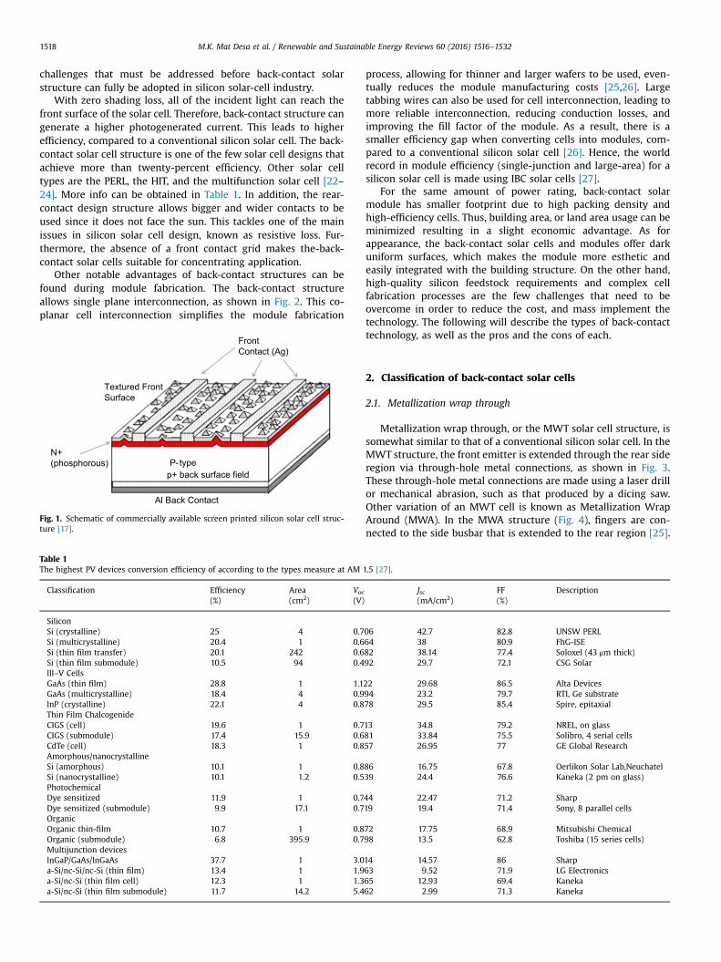
Metallization wrap through, or the MWT solar cell structure, issomewhat similar to that of a conventional silicon solar cell. In theMWT structure, the front emitter is extended through the rear sideregion via through-hole metal connections, as shown in Fig. 3.These through-hole metal connections are made using a laser drillor mechanical abrasion, such as that produced by a dicing saw.Other variation of an MWT cell is known as Metallization WrapAround (MWA). In the MWA structure (Fig. 4), fingers are con-nected to the side busbar that is extended to the rear region [25].
Fig. 2. Conventional silicon solar and back contact co-planar/single-plane (right) cell interconnection to form solar module [28].
Backside
Front side
Front contact grid
Negative Contact (-)
Positive Contact (+)
Through hole connection (emitter contact)
Base ContactInactive region/ Compensate region.
Fig. 3. MWT structure cross section [30] and solar cell (right). On the back surface the line busbar represents emitter busbar while the white circles represent base contact[31].
wafer
Front contact metallic paste
Extended metallic contact
Fig. 4. Screen printed extended metal paste over the edge of wafer to rear sidebusbar in MWA structure [25].
Voids in through hole metal contacts
Fig. 5. MWT solar cell through-hole connection cross-section [26]. Cavity in metalthrough-hole connection can lead to high series resistance and low the fill factor.
M.K. Mat Desa et al. / Renewable and Sustainable Energy Reviews 60 (2016) 1516–1532 1519
This is made by screen printing through the edge of the wafer,with busbar isolation on the backside.
The MWT structure has the advantage of reducing shadowinglosses, due to smaller busbar and finger size. Moreover, an addi-tional emitter region at the rear side helps capturing more pho-tocurrents [29]. This results in an increase in short-circuit currentdensity of the cell. Hence, a slight gain in cell level efficiency isexpected, compared to that of a conventional silicon solar cell[25,30]. Other main advantages of the MWT are co-planar cellinterconnection and dark uniform module appearances. In MWTstructure, front finger grids and through-hole connections assist inchanneling the photo-generated currents from the front surface tothe rear side busbar. Thus, a low carrier lifetime substrate, such asa multicrystalline wafer, can be used in MWT structures. In thefabrication process, hole drilling and emitter-base isolation are fewadditional steps required in comparison with a conventional sili-con solar cell.
These through holes can be drilled by using common laserequipment, such as an Nd-Yag laser tool. Emitter and base isolation
at the rear side can be achieved by mechanical means, such aslaser ablation, etching or a masking method, such as a diffusionbarrier. The isolation between the emitter and the base is not toocritical, since the geometry design is quite relaxed. One of thechallenges in the MWT structure is to develop reliable and low-resistivity through-hole connections [25,31]. Voids in through-hole connections (Fig. 5) would lead to a high series resistance anda low fill factor. Method such as short suction step after screenprinted metallization is used to achieve a good through-holeconnection [31]. Another issue encountered during MWT cellfabrication is shunting, due to the metal contact passing throughthe emitter region side.
Conventional fabrication processes and solar cell equipmentincluding screen printers, can be used to fabricate an MWT solarcell. The simple fabrication process makes MWT easily integratedinto the PV industry [31,32]. In laboratory or pilot projection,MWT solar cells have demonstrate efficiencies close to 16% on
Fig. 7. An example IBC solar cell structure with the rear contact that is in inter-digitated pattern by IMEC [71].
M.K. Mat Desa et al. / Renewable and Sustainable Energy Reviews 60 (2016) 1516–15321520
multicrystalline substrates [31]. Recent results has demonstratedan efficiencies of 19.6% on p-type mono-cast wafer and selectiveemitter technology [30]. MWT shows promising result on n-typeCZ wafer, with a 19.7% efficiency. Cell and module efficiencies areexpected to be greater than 20% in the nearest future. The ease offabrication, relaxed substrate quality requirements, and simplicityin the rear side pattern make MWT one of the favorites to becommercialized in the PV industry. In fact, some PV manufacturershave already commercialized MWT technology [33], while otherswould consider it as one of their product lines [34].
2.2. Emitter wrap through
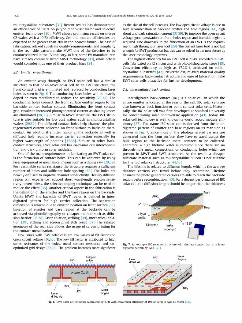
An emitter wrap through, or EWT solar cell has a similarstructure to that of an MWT solar cell. In an EWT structure, thefront contact grid is eliminated and replaced by conducting laserholes as seen in Fig. 6. The conducting laser holes will be heavilydoped or even metallized to reduce the resistivity [23,35]. Theconducting holes connect the front surface emitter region to thebackside emitter busbar contact. Eliminating the front contactgrid, results in increased photogenerated current as shading lossesare eliminated [18,36]. Similar to MWT structure, the EWT struc-ture is also suitable for low cost wafers such as multicrystallinewafers [29,37]. The diffused contact holes help channel the pho-togenerated current collected on front surface to backside metalcontact. An additional emitter region at the backside as well asdiffused hole regions increase carrier collection especially forhigher wavelength of photons [37,38]. Similar to other back-contact structures, EWT solar cell has co-planar cell interconnec-tion and dark uniform solar modules.
One of the main requirements in fabricating an EWT solar cellis the formation of contact holes. This can be achieved by usinglaser equipment or mechanical means such as a dicing saw [29,39].For reasonable series resistance the structure requires a sufficientnumber of holes and sufficient hole spacing [39]. The holes areheavily diffused to improve channel conductivity. Heavily diffusedregion will experience reduced short wavelength photon sensi-tivity nevertheless, the selective doping technique can be used toreduce the effect [35]. Another critical aspect in the fabrication isthe definition of the emitter and the base region on the backside.Unlike MWT, the backside of EWT region is defined in inter-digitated pattern for high carrier collection. The separationdimension is relaxed due to emitter location on front surface [18].Isolation of emitter and base region at the backside can beachieved via photolithography or cheaper method such as diffu-sion barrier [35,38], laser ablation/scribing [39], mechanical abla-tion [39], etching and screen print etch resist [37]. The relaxedgeometry of the rear side allows the usage of screen printing forthe contact metallization.
Few issues with EWT solar cells are low values of fill factor andopen circuit voltage [36,40]. The low fill factor is attributed to highseries resistance of the holes, metal contact resistance and un-optimized grid design [37,38]. The problem becomes more significant
Fig. 6. EWT solar cell structure fabricated by ISFH with con
as the size of the cell increases. The low open circuit voltage is due tohigh recombination in backside emitter and hole regions [41], highshunt and dark saturation current [37,39]. To improve the open circuitvoltage good passivation on front, holes region and backside region isrequired. One drawback in the fabrication of an EWT is the require-ment high throughput laser tool [29]. The current laser tool is not fastenough for EWT production but this can be solved in the near future asthe laser technology improves.
The highest efficiency for an EWT cell is 21.4%, recorded in EWTcells fabricated on FZ silicon and with photolithography steps [18].Conversion efficiency as high as 17.2% is achieved on multi-crystalline substrates [42]. Nevertheless, relaxed material qualityrequirements, back-contact structure and ease of fabrication makeEWT solar cells attractive for further development.
2.3. Interdigitated back contact
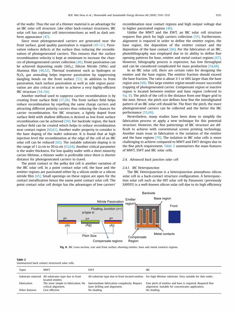
Interdigitated back-contact (IBC) is a solar cell in which theentire emitter is located at the rear of the cell. IBC solar cells arealso known as back junction or point contact solar cells. Histori-cally, the IBC solar cell was first developed at Stanford Universityfor concentrating solar photovoltaic application [43]. Today, IBCsolar cell technology is well known its world record module effi-ciency [27]. The name IBC solar cell is derived from the inter-digitated pattern of emitter and base regions on its rear side asshown in Fig. 7. Since most of the photogenerated carriers aregenerated near the front surface, they have to travel across thebulk region to the backside metal contacts to be collected.Therefore, a high lifetime wafer is required since there are nothrough-hole metal connections or conducting holes which arepresent in MWT and EWT structures. As the result, a cheapersubstrate material such as multicrystalline silicon is not suitablefor the IBC solar cell structure [44,45].
The lifetime is related to diffusion length, which is the averagedistance carriers can travel before they recombine. Lifetimeensures the photo generated carriers are able to reach the backsideregion before recombination [46]. For a decent performance of IBCsolar cell, the diffusion length should be longer than the thickness
version efficiency of 19% on large p type CZ wafer [42].
M.K. Mat Desa et al. / Renewable and Sustainable Energy Reviews 60 (2016) 1516–1532 1521
of the wafer. Thus the use of a thinner material is an advantage foran IBC solar cell structure. Like other back-contact structures, IBCsolar cell has coplanar cell interconnections as well as dark uni-form appearance [47].
Since most photogenerated carriers are generated near thefront surface, good quality passivation is required [47–51]. Passi-vation reduces defects at the surface thus reducing the recombi-nation of photogenerated carriers. This ensures that the surfacerecombination velocity is kept at minimum to increase the chan-ces of photogenerated carrier collection [46]. Front passivation canbe achieved depositing oxide (SiO2), Silicon Nitride (SiNx) andAlumina film [48,52]. Thermal treatment such as hydrogen orN2O2 gas annealing helps improve passivation by suppressingdangling bonds on the front surface [53]. In addition to frontpassivation, back surface passivation as well as side region passi-vation are also critical in order to achieve a very highly-efficientIBC structure [54–56].
Another method used to suppress carrier recombination is bycreating front surface field [57,58]. The front surface field helpsreduce recombination by repelling the same charge carriers andattracting different polarity carriers thus reducing the chances forcarrier recombination. For IBC structure, a lightly doped frontsurface field with shallow diffusion is desired as low front surfacerecombination can be achieved [59]. For backside region, the backsurface field can be created which helps to reduce recombinationnear contact region [60,61]. Another wafer property to consider isthe base doping of the wafer substrate. It is found that at highinjection level the recombination at the edge of the cell of an IBCsolar cell can be reduced [62]. The suitable substrate doping is inthe range of 1 Ω cm to 50 Ω cm [63,64]. Another critical parameteris the wafer thickness. For low quality wafer with a short minoritycarrier lifetime, a thinner wafer is preferable since there is shorterdistance for photogenerated carriers to travel.
The point contact or the polka dot cell is another variation ofthe IBC solar cell. In a point contact solar cell, the base and theemitter regions are passivated either by a silicon oxide or a siliconnitride film [65]. Small openings on these region are open for thecontact metallization hence the name point contact solar cell. Thepoint contact solar cell design has the advantages of low carriers'
Floating Junction (n+)
Nitride Passivatio
(Al) (Ag) (Al)
Pitch Size
p-type si
p+ p+n+
Compensate regions
Fig. 8. IBC cross-section, rear and front surface sho
Table 2Summarized back contact structured solar cells.
Types MWT EWT
Substrate material All substrates type due to frontlocated emitter.
All substrate type due to fro
Fabrication The most simple in fabrication. Nocritical alignment.
Intermediate fabrication comlaser drilling and alignment
Other features Cost effective No shading
recombination near contact regions and high output voltage dueto higher passivated regions [46].
Unlike the MWT and the EWT, an IBC solar cell structurerequires fine pitch for high carriers collection [55]. Furthermore,alignment is required in order to define the emitter region, thebase region, the deposition of the emitter contact and thedeposition of the base contact [66]. For the fabrication of an IBC,photolithography was employed due to its ability to define fineopening patterns for base, emitter and metal contact regions [67].However, lithography process is expensive, has low throughputand can be considered complicated for mass production [54,68].
In an IBC solar cell, there are certain rules for designing theemitter and the base region. The emitter fraction should exceedthe base fraction. The ratio is about 3:1 or 60% larger than the baseregion area [68]. This large emitter region would ensure successfultrapping of photogenerated carrier. Compensate region or inactiveregion is located between emitter and base region (referred toFig. 8). The pitch of the cell is the distance from one finger grid tothe next. Hence, the pitch size defines how fine the interdigitatedpattern of an IBC solar cell should be. The finer the pitch, the morephotogenerated carriers can be collected and the better the IBCperformance [55,69].
Nevertheless, many studies have been done to simplify thefabrication process or apply a new technique for this potentialstructure. However, the fine patternings of IBC structure are dif-ficult to achieve with conventional screen printing technology.Another main issue in fabrication is the isolation of the emitterand the base regions [70]. The isolation in IBC solar cells is morechallenging to achieve compared to MWT and EWT designs due tothe fine pitch requirement. Table 2 summarizes the main featuresof MWT, EWT and IBC solar cells.
2.4. Advanced back junction solar cell
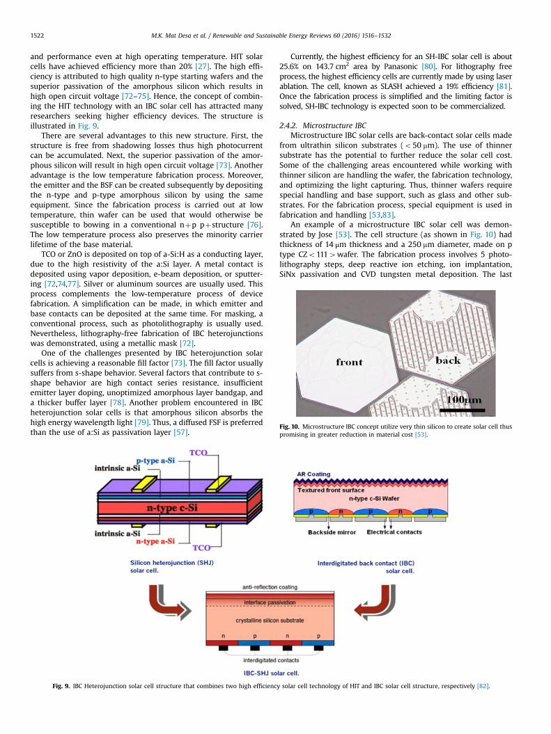
2.4.1. IBC HeterojunctionThe IBC Heterojunction is a heterojunction amorphous silicon
solar cell in a back-contact structure configuration. A heterojunc-tion solar cell such as the HIT solar cell by Panasonic (previouslySANYO) is a well-known silicon solar cell due to its high efficiency
Front
Backside
Metal contactsCompensate Region
Emitter region
Base regionn
wing emitter, base and metal contacts regions.
IBC
nt located emitter. For high lifetime substrate. Very suitable for thin wafer.
plexity. Require.
Fine pitch of emitter and base is required. Required finealignment. Suitable for concentrator application.No shading
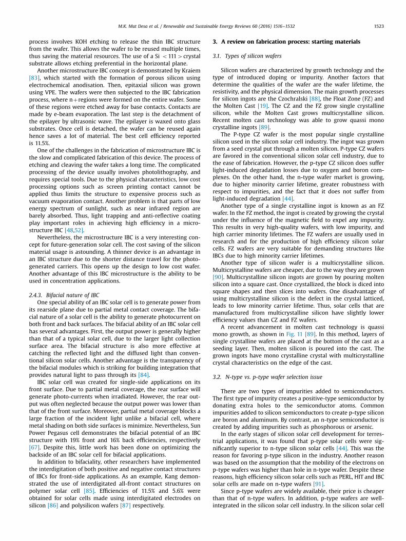
Fig. 10. Microstructure IBC concept utilize very thin silicon to create solar cell thuspromising in greater reduction in material cost [53].
M.K. Mat Desa et al. / Renewable and Sustainable Energy Reviews 60 (2016) 1516–15321522
and performance even at high operating temperature. HIT solarcells have achieved efficiency more than 20% [27]. The high effi-ciency is attributed to high quality n-type starting wafers and thesuperior passivation of the amorphous silicon which results inhigh open circuit voltage [72–75]. Hence, the concept of combin-ing the HIT technology with an IBC solar cell has attracted manyresearchers seeking higher efficiency devices. The structure isillustrated in Fig. 9.
There are several advantages to this new structure. First, thestructure is free from shadowing losses thus high photocurrentcan be accumulated. Next, the superior passivation of the amor-phous silicon will result in high open circuit voltage [73]. Anotheradvantage is the low temperature fabrication process. Moreover,the emitter and the BSF can be created subsequently by depositingthe n-type and p-type amorphous silicon by using the sameequipment. Since the fabrication process is carried out at lowtemperature, thin wafer can be used that would otherwise besusceptible to bowing in a conventional nþp pþstructure [76].The low temperature process also preserves the minority carrierlifetime of the base material.
TCO or ZnO is deposited on top of a-Si:H as a conducting layer,due to the high resistivity of the a:Si layer. A metal contact isdeposited using vapor deposition, e-beam deposition, or sputter-ing [72,74,77]. Silver or aluminum sources are usually used. Thisprocess complements the low-temperature process of devicefabrication. A simplification can be made, in which emitter andbase contacts can be deposited at the same time. For masking, aconventional process, such as photolithography is usually used.Nevertheless, lithography-free fabrication of IBC heterojunctionswas demonstrated, using a metallic mask [72].
One of the challenges presented by IBC heterojunction solarcells is achieving a reasonable fill factor [73]. The fill factor usuallysuffers from s-shape behavior. Several factors that contribute to s-shape behavior are high contact series resistance, insufficientemitter layer doping, unoptimized amorphous layer bandgap, anda thicker buffer layer [78]. Another problem encountered in IBCheterojunction solar cells is that amorphous silicon absorbs thehigh energy wavelength light [79]. Thus, a diffused FSF is preferredthan the use of a:Si as passivation layer [57].
Fig. 9. IBC Heterojunction solar cell structure that combines two high efficiency
Currently, the highest efficiency for an SH-IBC solar cell is about25.6% on 143.7 cm2 area by Panasonic [80]. For lithography freeprocess, the highest efficiency cells are currently made by using laserablation. The cell, known as SLASH achieved a 19% efficiency [81].Once the fabrication process is simplified and the limiting factor issolved, SH-IBC technology is expected soon to be commercialized.
2.4.2. Microstructure IBCMicrostructure IBC solar cells are back-contact solar cells made
from ultrathin silicon substrates (o50 mm). The use of thinnersubstrate has the potential to further reduce the solar cell cost.Some of the challenging areas encountered while working withthinner silicon are handling the wafer, the fabrication technology,and optimizing the light capturing. Thus, thinner wafers requirespecial handling and base support, such as glass and other sub-strates. For the fabrication process, special equipment is used infabrication and handling [53,83].
An example of a microstructure IBC solar cell was demon-strated by Jose [53]. The cell structure (as shown in Fig. 10) hadthickness of 14 μm thickness and a 250 mm diameter, made on ptype CZo1114wafer. The fabrication process involves 5 photo-lithography steps, deep reactive ion etching, ion implantation,SiNx passivation and CVD tungsten metal deposition. The last
solar cell technology of HIT and IBC solar cell structure, respectively [82].
M.K. Mat Desa et al. / Renewable and Sustainable Energy Reviews 60 (2016) 1516–1532 1523
process involves KOH etching to release the thin IBC structurefrom the wafer. This allows the wafer to be reused multiple times,thus saving the material resources. The use of a Si o1114crystalsubstrate allows etching preferential in the horizontal plane.
Another microstructure IBC concept is demonstrated by Kraiem[83], which started with the formation of porous silicon usingelectrochemical anodisation. Then, epitaxial silicon was grownusing VPE. The wafers were then subjected to the IBC fabricationprocess, where nþregions were formed on the entire wafer. Someof these regions were etched away for base contacts. Contacts aremade by e-beam evaporation. The last step is the detachment ofthe epilayer by ultrasonic wave. The epilayer is waxed onto glasssubstrates. Once cell is detached, the wafer can be reused againhence saves a lot of material. The best cell efficiency reportedis 11.5%.
One of the challenges in the fabrication of microstructure IBC isthe slow and complicated fabrication of this device. The process ofetching and cleaving the wafer takes a long time. The complicatedprocessing of the device usually involves photolithography, andrequires special tools. Due to the physical characteristics, low costprocessing options such as screen printing contact cannot beapplied thus limits the structure to expensive process such asvacuum evaporation contact. Another problem is that parts of lowenergy spectrum of sunlight, such as near infrared region arebarely absorbed. Thus, light trapping and anti-reflective coatingplay important roles in achieving high efficiency in a micro-structure IBC [48,52].
Nevertheless, the microstructure IBC is a very interesting con-cept for future-generation solar cell. The cost saving of the siliconmaterial usage is astounding. A thinner device is an advantage inan IBC structure due to the shorter distance travel for the photo-generated carriers. This opens up the design to low cost wafer.Another advantage of this IBC microstructure is the ability to beused in concentration applications.
2.4.3. Bifacial nature of IBCOne special ability of an IBC solar cell is to generate power from
its rearside plane due to partial metal contact coverage. The bifa-cial nature of a solar cell is the ability to generate photocurrent onboth front and back surfaces. The bifacial ability of an IBC solar cellhas several advantages. First, the output power is generally higherthan that of a typical solar cell, due to the larger light collectionsurface area. The bifacial structure is also more effective atcatching the reflected light and the diffused light than conven-tional silicon solar cells. Another advantage is the transparency ofthe bifacial modules which is striking for building integration thatprovides natural light to pass through its [84].
IBC solar cell was created for single-side applications on itsfront surface. Due to partial metal coverage, the rear surface willgenerate photo-currents when irradiated. However, the rear out-put was often neglected because the output power was lower thanthat of the front surface. Moreover, partial metal coverage blocks alarge fraction of the incident light unlike a bifacial cell, wheremetal shading on both side surfaces is minimize. Nevertheless, SunPower Pegasus cell demonstrates the bifacial potential of an IBCstructure with 19% front and 16% back efficiencies, respectively[67]. Despite this, little work has been done on optimizing thebackside of an IBC solar cell for bifacial applications.
In addition to bifaciality, other researchers have implementedthe interdigitation of both positive and negative contact structuresof IBCs for front-side applications. As an example, Kang demon-strated the use of interdigitated all-front contact structures onpolymer solar cell [85]. Efficiencies of 11.5% and 5.6% wereobtained for solar cells made using interdigitated electrodes onsilicon [86] and polysilicon wafers [87] respectively.
3. A review on fabrication process: starting materials
3.1. Types of silicon wafers
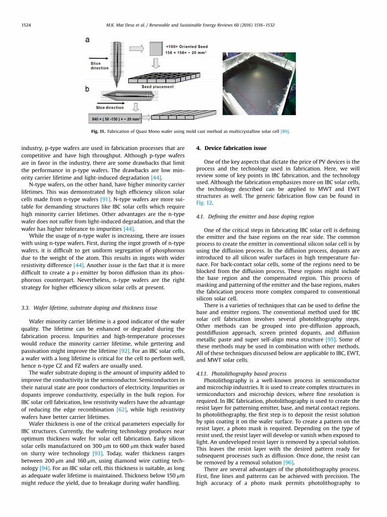
Silicon wafers are characterized by growth technology and thetype of introduced doping or impurity. Another factors thatdetermine the qualities of the wafer are the wafer lifetime, theresistivity, and the physical dimension. The main growth processesfor silicon ingots are the Czochralski [88], the Float Zone (FZ) andthe Molten Cast [19]. The CZ and the FZ grow single crystallinesilicon, while the Molten Cast grows multicrystalline silicon.Recent molten cast technology was able to grow quassi monocrystalline ingots [89].
The P-type CZ wafer is the most popular single crystallinesilicon used in the silicon solar cell industry. The ingot was grownfrom a seed crystal put through a molten silicon. P-type CZ wafersare favored in the conventional silicon solar cell industry, due tothe ease of fabrication. However, the p-type CZ silicon does sufferlight-induced degradation losses due to oxygen and boron com-plexes. On the other hand, the n-type wafer market is growing,due to higher minority carrier lifetime, greater robustness withrespect to impurities, and the fact that it does not suffer fromlight-induced degradation [44].
Another type of a single crystalline ingot is known as an FZwafer. In the FZ method, the ingot is created by growing the crystalunder the influence of the magnetic field to expel any impurity.This results in very high-quality wafers, with low impurity, andhigh carrier minority lifetimes. The FZ wafers are usually used inresearch and for the production of high efficiency silicon solarcells. FZ wafers are very suitable for demanding structures likeIBCs due to high minority carrier lifetimes.
Another type of silicon wafer is a multicrystalline silicon.Multicrystalline wafers are cheaper, due to the way they are grown[90]. Multicrystalline silicon ingots are grown by pouring moltensilicon into a square cast. Once crystallized, the block is diced intosquare shapes and then slices into wafers. One disadvantage ofusing multicrystalline silicon is the defect in the crystal latticed,leads to low minority carrier lifetime. Thus, solar cells that aremanufactured from multicrystalline silicon have slightly lowerefficiency values than CZ and FZ wafers.
A recent advancement in molten cast technology is quassimono growth, as shown in Fig. 11 [89]. In this method, layers ofsingle crystalline wafers are placed at the bottom of the cast as aseeding layer. Then, molten silicon is poured into the cast. Thegrown ingots have mono crystalline crystal with multicrystallinecrystal characteristics on the edge of the cast.
3.2. N-type vs. p-type wafer selection issue
There are two types of impurities added to semiconductors.The first type of impurity creates a positive-type semiconductor bydonating extra holes to the semiconductor atoms. Commonimpurities added to silicon semiconductors to create p-type siliconare boron and aluminum. By contrast, an n-type semiconductor iscreated by adding impurities such as phosphorous or arsenic.
In the early stages of silicon solar cell development for terres-trial applications, it was found that p-type solar cells were sig-nificantly superior to n-type silicon solar cells [44]. This was thereason for favoring p-type silicon in the industry. Another reasonwas based on the assumption that the mobility of the electrons onp-type wafers was higher than hole in n-type wafer. Despite thesereasons, high efficiency silicon solar cells such as PERL, HIT and IBCsolar cells are made on n-type wafers [91].
Since p-type wafers are widely available, their price is cheaperthan that of n-type wafers. In addition, p-type wafers are well-integrated in the silicon solar cell industry. In the silicon solar cell
Fig. 11. Fabrication of Quasi Mono wafer using mold cast method as multicrystalline solar cell [89].
M.K. Mat Desa et al. / Renewable and Sustainable Energy Reviews 60 (2016) 1516–15321524
industry, p-type wafers are used in fabrication processes that arecompetitive and have high throughput. Although p-type wafersare in favor in the industry, there are some drawbacks that limitthe performance in p-type wafers. The drawbacks are low min-ority carrier lifetime and light-induced degradation [44].
N-type wafers, on the other hand, have higher minority carrierlifetimes. This was demonstrated by high efficiency silicon solarcells made from n-type wafers [91]. N-type wafers are more sui-table for demanding structures like IBC solar cells which requirehigh minority carrier lifetimes. Other advantages are the n-typewafer does not suffer from light-induced degradation, and that thewafer has higher tolerance to impurities [44].
While the usage of n-type wafer is increasing, there are issueswith using n-type wafers. First, during the ingot growth of n-typewafers, it is difficult to get uniform segregation of phosphorousdue to the weight of the atom. This results in ingots with widerresistivity difference [44]. Another issue is the fact that it is moredifficult to create a pþemitter by boron diffusion than its phos-phorous counterpart. Nevertheless, n-type wafers are the rightstrategy for higher efficiency silicon solar cells at present.
3.3. Wafer lifetime, substrate doping and thickness issue
Wafer minority carrier lifetime is a good indicator of the waferquality. The lifetime can be enhanced or degraded during thefabrication process. Impurities and high-temperature processeswould reduce the minority carrier lifetime, while gettering andpassivation might improve the lifetime [92]. For an IBC solar cells,a wafer with a long lifetime is critical for the cell to perform well,hence n-type CZ and FZ wafers are usually used.
The wafer substrate doping is the amount of impurity added toimprove the conductivity in the semiconductor. Semiconductors intheir natural state are poor conductors of electricity. Impurities ordopants improve conductivity, especially in the bulk region. ForIBC solar cell fabrication, low resistivity wafers have the advantageof reducing the edge recombination [62], while high resistivitywafers have better carrier lifetimes.
Wafer thickness is one of the critical parameters especially forIBC structures. Currently, the wafering technology produces nearoptimum thickness wafer for solar cell fabrication. Early siliconsolar cells manufactured on 300 mm to 600 mm thick wafer basedon slurry wire technology [93]. Today, wafer thickness rangesbetween 200 μm and 160 μm, using diamond wire cutting tech-nology [94]. For an IBC solar cell, this thickness is suitable, as longas adequate wafer lifetime is maintained. Thickness below 150 μmmight reduce the yield, due to breakage during wafer handling.
4. Device fabrication issue
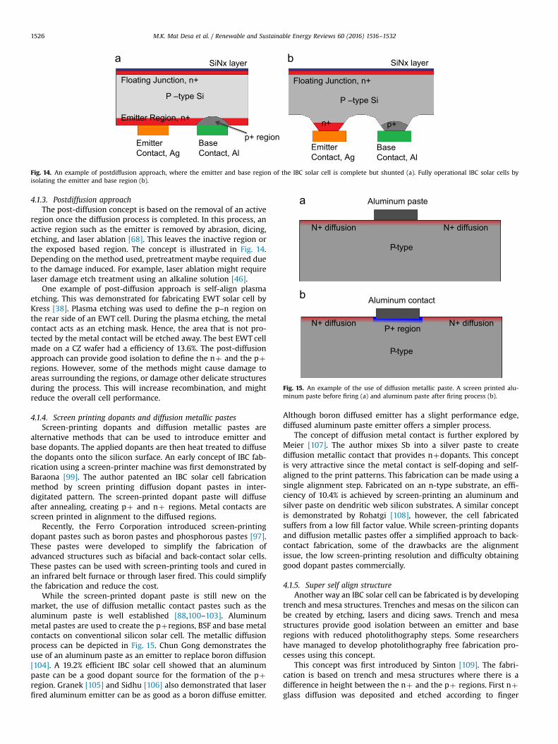
One of the key aspects that dictate the price of PV devices is theprocess and the technology used in fabrication. Here, we willreview some of key points in IBC fabrication, and the technologyused. Although the fabrication emphasizes more on IBC solar cells,the technology described can be applied to MWT and EWTstructures as well. The generic fabrication flow can be found inFig. 12.
4.1. Defining the emitter and base doping region
One of the critical steps in fabricating IBC solar cell is definingthe emitter and the base regions on the rear side. The commonprocess to create the emitter in conventional silicon solar cell is byusing the diffusion process. In the diffusion process, dopants areintroduced to all silicon wafer surfaces in high temperature fur-nace. For back-contact solar cells, some of the regions need to beblocked from the diffusion process. These regions might includethe base region and the compensated region. This process ofmasking and patterning of the emitter and the base regions, makesthe fabrication process more complex compared to conventionalsilicon solar cell.
There is a varieties of techniques that can be used to define thebase and emitter regions. The conventional method used for IBCsolar cell fabrication involves several photolithography steps.Other methods can be grouped into pre-diffusion approach,postdiffusion approach, screen printed dopants, and diffusionmetallic paste and super self-align mesa structure [95]. Some ofthese methods may be used in combination with other methods.All of these techniques discussed below are applicable to IBC, EWT,and MWT solar cells.
4.1.1. Photolithography based processPhotolithography is a well-known process in semiconductor
and microchip industries. It is used to create complex structures insemiconductors and microchip devices, where fine resolution isrequired. In IBC fabrication, photolithography is used to create theresist layer for patterning emitter, base, and metal contact regions.In photolithography, the first step is to deposit the resist solutionby spin coating it on the wafer surface. To create a pattern on theresist layer, a photo mask is required. Depending on the type ofresist used, the resist layer will develop or vanish when exposed tolight. An undeveloped resist layer is removed by a special solution.This leaves the resist layer with the desired pattern ready forsubsequent processes such as diffusion. Once done, the resist canbe removed by a removal solution [96].
There are several advantages of the photolithography process.First, fine lines and patterns can be achieved with precision. Thehigh accuracy of a photo mask permits photolithography to
Fig. 12. Generic fabrication flow; a) saw damage and cleaning b) texturing c)defining emitter and base region d) formation front surface field and antireflectivecoating e) defining metal contacts.
P-type
Diffusion barrier paste prints
P-type
N+ diffusionN+ diffusion N+ diffusion
Diffusion barrier paste prints
Fig. 13. An example of the use of diffusion barrier for isolation. Before diffusionprocess (a) and after diffusion process (b).
M.K. Mat Desa et al. / Renewable and Sustainable Energy Reviews 60 (2016) 1516–1532 1525
achieve fine lines, even on micrometer and nanometer scales.Other advantages are good alignment and accuracy. Photo-lithography has alignment capability that is important whendefining the emitter and the base regions. Besides, the resist onthe wafer is able to withstand high temperatures and harsh che-mical processes such as diffusion and the etching process [96].
While photolithography is a great tool for fabricating back-contact solar cells, high costs and low throughput are the draw-backs [46,55,68]. Usually about 4–6 photolithography steps arerequired in order to fabricate an IBC solar cell. The costs ofdeveloper solutions and photo mask design increase the overallcost of the solar cell. In addition, for each lithography step, thereare several sub-steps required. Thus photolithography is con-sidered low-throughput and complicated.
For a photolithography process, the cost is justified when IBCsolar cells are used in concentrating applications. For one sunapplication, the goal was to reduce the lithography process to asingle step. By reducing the number of lithography steps, the cost
can be reduced. For example, Cudzinovic demonstrated reducingthe number of photolithography steps from 6 to 3 can reduce thefabrication cost by as much as 30%, with only a slight reduction inefficiency [67].
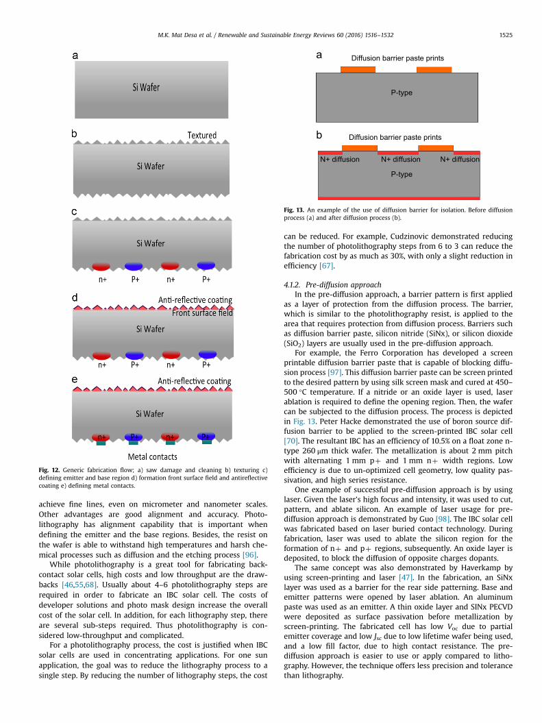
4.1.2. Pre-diffusion approachIn the pre-diffusion approach, a barrier pattern is first applied
as a layer of protection from the diffusion process. The barrier,which is similar to the photolithography resist, is applied to thearea that requires protection from diffusion process. Barriers suchas diffusion barrier paste, silicon nitride (SiNx), or silicon dioxide(SiO2) layers are usually used in the pre-diffusion approach.
For example, the Ferro Corporation has developed a screenprintable diffusion barrier paste that is capable of blocking diffu-sion process [97]. This diffusion barrier paste can be screen printedto the desired pattern by using silk screen mask and cured at 450–500 °C temperature. If a nitride or an oxide layer is used, laserablation is required to define the opening region. Then, the wafercan be subjected to the diffusion process. The process is depictedin Fig. 13. Peter Hacke demonstrated the use of boron source dif-fusion barrier to be applied to the screen-printed IBC solar cell[70]. The resultant IBC has an efficiency of 10.5% on a float zone n-type 260 μm thick wafer. The metallization is about 2 mm pitchwith alternating 1 mm pþ and 1 mm nþ width regions. Lowefficiency is due to un-optimized cell geometry, low quality pas-sivation, and high series resistance.
One example of successful pre-diffusion approach is by usinglaser. Given the laser's high focus and intensity, it was used to cut,pattern, and ablate silicon. An example of laser usage for pre-diffusion approach is demonstrated by Guo [98]. The IBC solar cellwas fabricated based on laser buried contact technology. Duringfabrication, laser was used to ablate the silicon region for theformation of nþ and pþ regions, subsequently. An oxide layer isdeposited, to block the diffusion of opposite charges dopants.
The same concept was also demonstrated by Haverkamp byusing screen-printing and laser [47]. In the fabrication, an SiNxlayer was used as a barrier for the rear side patterning. Base andemitter patterns were opened by laser ablation. An aluminumpaste was used as an emitter. A thin oxide layer and SINx PECVDwere deposited as surface passivation before metallization byscreen-printing. The fabricated cell has low Voc due to partialemitter coverage and low Jsc due to low lifetime wafer being used,and a low fill factor, due to high contact resistance. The pre-diffusion approach is easier to use or apply compared to litho-graphy. However, the technique offers less precision and tolerancethan lithography.
Emitter Contact, Ag
Base Contact, Al
P –type Si
p+ region
Emitter Region, n+
Floating Junction, n+
SiNx layer
Emitter Contact, Ag
Base Contact, Al
P –type Si
p+
Floating Junction, n+
SiNx layer
n+
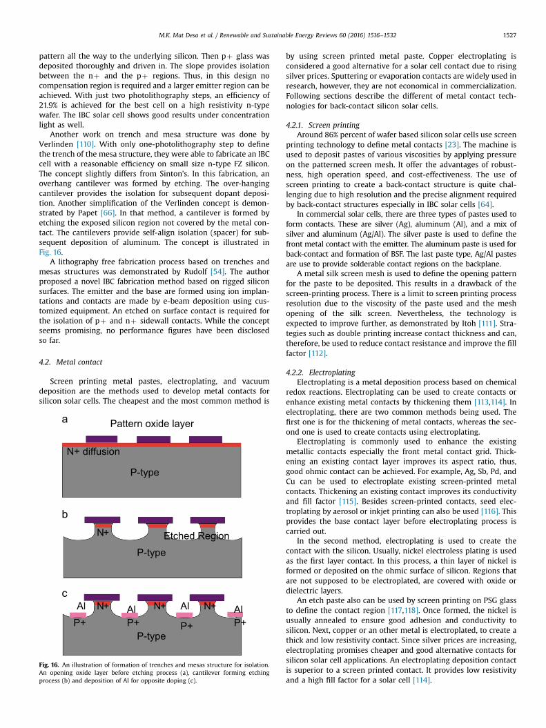
Fig. 14. An example of postdiffusion approach, where the emitter and base region of the IBC solar cell is complete but shunted (a). Fully operational IBC solar cells byisolating the emitter and base region (b).
N+ diffusion
P-type
Aluminum paste
P+ region
N+ diffusion
Aluminum contact
P-type
N+ diffusionN+ diffusion
Fig. 15. An example of the use of diffusion metallic paste. A screen printed alu-minum paste before firing (a) and aluminum paste after firing process (b).
M.K. Mat Desa et al. / Renewable and Sustainable Energy Reviews 60 (2016) 1516–15321526
4.1.3. Postdiffusion approachThe post-diffusion concept is based on the removal of an active
region once the diffusion process is completed. In this process, anactive region such as the emitter is removed by abrasion, dicing,etching, and laser ablation [68]. This leaves the inactive region orthe exposed based region. The concept is illustrated in Fig. 14.Depending on the method used, pretreatment maybe required dueto the damage induced. For example, laser ablation might requirelaser damage etch treatment using an alkaline solution [46].
One example of post-diffusion approach is self-align plasmaetching. This was demonstrated for fabricating EWT solar cell byKress [38]. Plasma etching was used to define the p–n region onthe rear side of an EWT cell. During the plasma etching, the metalcontact acts as an etching mask. Hence, the area that is not pro-tected by the metal contact will be etched away. The best EWT cellmade on a CZ wafer had a efficiency of 13.6%. The post-diffusionapproach can provide good isolation to define the nþ and the pþregions. However, some of the methods might cause damage toareas surrounding the regions, or damage other delicate structuresduring the process. This will increase recombination, and mightreduce the overall cell performance.
4.1.4. Screen printing dopants and diffusion metallic pastesScreen-printing dopants and diffusion metallic pastes are
alternative methods that can be used to introduce emitter andbase dopants. The applied dopants are then heat treated to diffusethe dopants onto the silicon surface. An early concept of IBC fab-rication using a screen-printer machine was first demonstrated byBaraona [99]. The author patented an IBC solar cell fabricationmethod by screen printing diffusion dopant pastes in inter-digitated pattern. The screen-printed dopant paste will diffuseafter annealing, creating pþ and nþ regions. Metal contacts arescreen printed in alignment to the diffused regions.
Recently, the Ferro Corporation introduced screen-printingdopant pastes such as boron pastes and phosphorous pastes [97].These pastes were developed to simplify the fabrication ofadvanced structures such as bifacial and back-contact solar cells.These pastes can be used with screen-printing tools and cured inan infrared belt furnace or through laser fired. This could simplifythe fabrication and reduce the cost.
While the screen-printed dopant paste is still new on themarket, the use of diffusion metallic contact pastes such as thealuminum paste is well established [88,100–103]. Aluminummetal pastes are used to create the pþregions, BSF and base metalcontacts on conventional silicon solar cell. The metallic diffusionprocess can be depicted in Fig. 15. Chun Gong demonstrates theuse of an aluminum paste as an emitter to replace boron diffusion[104]. A 19.2% efficient IBC solar cell showed that an aluminumpaste can be a good dopant source for the formation of the pþregion. Granek [105] and Sidhu [106] also demonstrated that laserfired aluminum emitter can be as good as a boron diffuse emitter.
Although boron diffused emitter has a slight performance edge,diffused aluminum paste emitter offers a simpler process.
The concept of diffusion metal contact is further explored byMeier [107]. The author mixes Sb into a silver paste to creatediffusion metallic contact that provides nþdopants. This conceptis very attractive since the metal contact is self-doping and self-aligned to the print patterns. This fabrication can be made using asingle alignment step. Fabricated on an n-type substrate, an effi-ciency of 10.4% is achieved by screen-printing an aluminum andsilver paste on dendritic web silicon substrates. A similar conceptis demonstrated by Rohatgi [108], however, the cell fabricatedsuffers from a low fill factor value. While screen-printing dopantsand diffusion metallic pastes offer a simplified approach to back-contact fabrication, some of the drawbacks are the alignmentissue, the low screen-printing resolution and difficulty obtaininggood dopant pastes commercially.
4.1.5. Super self align structureAnother way an IBC solar cell can be fabricated is by developing
trench and mesa structures. Trenches and mesas on the silicon canbe created by etching, lasers and dicing saws. Trench and mesastructures provide good isolation between an emitter and baseregions with reduced photolithography steps. Some researchershave managed to develop photolithography free fabrication pro-cesses using this concept.
This concept was first introduced by Sinton [109]. The fabri-cation is based on trench and mesa structures where there is adifference in height between the nþ and the pþ regions. First nþglass diffusion was deposited and etched according to finger
M.K. Mat Desa et al. / Renewable and Sustainable Energy Reviews 60 (2016) 1516–1532 1527
pattern all the way to the underlying silicon. Then pþ glass wasdeposited thoroughly and driven in. The slope provides isolationbetween the nþ and the pþ regions. Thus, in this design nocompensation region is required and a larger emitter region can beachieved. With just two photolithography steps, an efficiency of21.9% is achieved for the best cell on a high resistivity n-typewafer. The IBC solar cell shows good results under concentrationlight as well.
Another work on trench and mesa structure was done byVerlinden [110]. With only one-photolithography step to definethe trench of the mesa structure, they were able to fabricate an IBCcell with a reasonable efficiency on small size n-type FZ silicon.The concept slightly differs from Sinton's. In this fabrication, anoverhang cantilever was formed by etching. The over-hangingcantilever provides the isolation for subsequent dopant deposi-tion. Another simplification of the Verlinden concept is demon-strated by Papet [66]. In that method, a cantilever is formed byetching the exposed silicon region not covered by the metal con-tact. The cantilevers provide self-align isolation (spacer) for sub-sequent deposition of aluminum. The concept is illustrated inFig. 16.
A lithography free fabrication process based on trenches andmesas structures was demonstrated by Rudolf [54]. The authorproposed a novel IBC fabrication method based on rigged siliconsurfaces. The emitter and the base are formed using ion implan-tations and contacts are made by e-beam deposition using cus-tomized equipment. An etched on surface contact is required forthe isolation of pþ and nþ sidewall contacts. While the conceptseems promising, no performance figures have been disclosedso far.
4.2. Metal contact
Screen printing metal pastes, electroplating, and vacuumdeposition are the methods used to develop metal contacts forsilicon solar cells. The cheapest and the most common method is
P-type
P-type
N+ diffusion
Pattern oxide layer
P-type
Etched Region
P+ P+ P+ P+
N+
N+ N+ N+ AlAlAl Al
Fig. 16. An illustration of formation of trenches and mesas structure for isolation.An opening oxide layer before etching process (a), cantilever forming etchingprocess (b) and deposition of Al for opposite doping (c).
by using screen printed metal paste. Copper electroplating isconsidered a good alternative for a solar cell contact due to risingsilver prices. Sputtering or evaporation contacts are widely used inresearch, however, they are not economical in commercialization.Following sections describe the different of metal contact tech-nologies for back-contact silicon solar cells.
4.2.1. Screen printingAround 86% percent of wafer based silicon solar cells use screen
printing technology to define metal contacts [23]. The machine isused to deposit pastes of various viscosities by applying pressureon the patterned screen mesh. It offer the advantages of robust-ness, high operation speed, and cost-effectiveness. The use ofscreen printing to create a back-contact structure is quite chal-lenging due to high resolution and the precise alignment requiredby back-contact structures especially in IBC solar cells [64].
In commercial solar cells, there are three types of pastes used toform contacts. These are silver (Ag), aluminum (Al), and a mix ofsilver and aluminum (Ag/Al). The silver paste is used to define thefront metal contact with the emitter. The aluminum paste is used forback-contact and formation of BSF. The last paste type, Ag/Al pastesare use to provide solderable contact regions on the backplane.
A metal silk screen mesh is used to define the opening patternfor the paste to be deposited. This results in a drawback of thescreen-printing process. There is a limit to screen printing processresolution due to the viscosity of the paste used and the meshopening of the silk screen. Nevertheless, the technology isexpected to improve further, as demonstrated by Itoh [111]. Stra-tegies such as double printing increase contact thickness and can,therefore, be used to reduce contact resistance and improve the fillfactor [112].
4.2.2. ElectroplatingElectroplating is a metal deposition process based on chemical
redox reactions. Electroplating can be used to create contacts orenhance existing metal contacts by thickening them [113,114]. Inelectroplating, there are two common methods being used. Thefirst one is for the thickening of metal contacts, whereas the sec-ond one is used to create contacts using electroplating.
Electroplating is commonly used to enhance the existingmetallic contacts especially the front metal contact grid. Thick-ening an existing contact layer improves its aspect ratio, thus,good ohmic contact can be achieved. For example, Ag, Sb, Pd, andCu can be used to electroplate existing screen-printed metalcontacts. Thickening an existing contact improves its conductivityand fill factor [115]. Besides screen-printed contacts, seed elec-troplating by aerosol or inkjet printing can also be used [116]. Thisprovides the base contact layer before electroplating process iscarried out.
In the second method, electroplating is used to create thecontact with the silicon. Usually, nickel electroless plating is usedas the first layer contact. In this process, a thin layer of nickel isformed or deposited on the ohmic surface of silicon. Regions thatare not supposed to be electroplated, are covered with oxide ordielectric layers.
An etch paste also can be used by screen printing on PSG glassto define the contact region [117,118]. Once formed, the nickel isusually annealed to ensure good adhesion and conductivity tosilicon. Next, copper or an other metal is electroplated, to create athick and low resistivity contact. Since silver prices are increasing,electroplating promises cheaper and good alternative contacts forsilicon solar cell applications. An electroplating deposition contactis superior to a screen printed contact. It provides low resistivityand a high fill factor for a solar cell [114].
M.K. Mat Desa et al. / Renewable and Sustainable Energy Reviews 60 (2016) 1516–15321528
4.2.3. Vacuum based deposition contactsVacuum based metal depositions such as metal evaporation,
metal sputtering or beam deposition are used to deposit highquality contacts. Solar cells fabricated using these techniques showsuperior fill factors to those made using screen printing metalcontacts due to the pure metal source used [116]. In metal eva-poration contacts, source materials such as titanium, palladium,aluminum, or silver, can be used. The targeted solar cells and thesource material are then subjected to the vacuum state. The sourcematerial is heated up, and in the vacuum state, it is vaporized atmuch lower temperature. The vaporized metal sometimes directedby electric field that is used to direct the vaporized metal to thetarget solar cell. For patterning the front metal contact, an openingmask is used.
Vacuum-based depositions usually create a thin layer of metalcontact. Sometimes more than one source material is used, toachieve good conductivity and solderable contacts. The need forthe vacuum state, as well as high equipment and material costsmake this type of deposition expensive [119]. It is often used inresearch laboratories or to produce very high-efficiency solar cells.
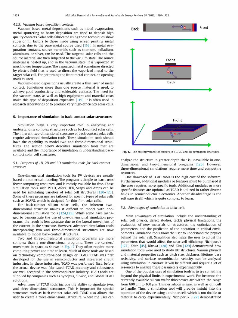
Fig. 17. The axis movement of carriers in 1D, 2D and 3D simulation structures.
5. Importance of simulation in back-contact solar structures
Simulation plays a very important role in analyzing andunderstanding complex structures such as back-contact solar cells.The inherent two-dimensional structure of back-contact solar cellsrequire advanced simulation tools. These simulation tools shouldhave the capability to model two and three-dimensional struc-tures. The section below describes simulation tools that areavailable and the importance of simulation in understanding back-contact solar cell structures.
5.1. Prospects of 1D, 2D and 3D simulation tools for back contactstructure
One-dimensional simulation tools for PV devices are usuallybased on numerical modeling. The program is simple to learn, usesfewer computing resources, and is mostly available for free. Thesesimulation tools such PC1D, Afors HEX, Scaps and Amps can beused for simulating varieties of solar cell structures [120–123].Some of these programs are tailored for specific types of solar cellssuch as SCAPS, which is designed for thin-film solar cells.
For back-contact silicon solar cells, the inherent two-dimensional structure makes it difficult to model with one-dimensional simulation tools [124,125]. While some have mana-ged to demonstrate the use of one-dimensional simulation pro-grams, the result is less accurate due to the lateral movement ofthe current in the structure. However, advanced simulation toolsincorporating two and three-dimensional structures are nowavailable to model back-contact structures.
Two and three-dimensional simulation programs are morecomplex than a one-dimensional programs. There are carriers'movement in space as shown in Fig. 17 They often require morecomputing power and time to learn. Much of these tools are basedon technology computer-aided design or TCAD. TCAD was firstdeveloped for the use in semiconductor and integrated circuitindustries. In these industries, TCAD was performed first, beforethe actual device was fabricated. TCAD accuracy and robustnessare well accepted in the semiconductor industry. TCAD tools aresupplied by companies such as Synopsis, Silvaco, and Global TCADsolutions.
Advantages of TCAD tools include the ability to simulate two,and three-dimensional structures. This is important for specialstructures such as back-contact solar cell. TCAD also allows theuser to create a three-dimensional structure, where the user can
analyze the structure in greater depth that is unavailable in one-dimensional and two-dimensional programs [126]. However,three-dimensional simulations require more time and computingresources.
One drawback of TCAD tools is the high cost of the software.Furthermore, additional modules or features must be purchased ifthe user requires more specific tools. Additional modules or morespecific features are optional, as TCAD is utilized in rather diversefields in semiconductor electronics. Another disadvantage is thesoftware itself, which is quite complex to learn.
5.2. Advantages of simulation in solar cells
Main advantages of simulation include the understanding ofsolar cell physics, defect studies, tackle physical limitations, theevaluation of new materials or structures, the optimization ofparameters, and the prediction of the operation in critical envir-onments. Simulation tools allow the user to understand the physicsbehind the solar cell. Simulation also helps the user to adjust theparameters that would affect the solar cell efficiency. Nichiporuk[127], Keith [45], Kluska [128] and Kim [129] demonstrated howsimulation tools were used to study IBC structures. Various physicaland material properties such as pitch size, thickness, lifetime, baseresistivity, and surface recombination velocity, can be analyzedusing simulation. In contrast, it will be difficult and require a lot ofresources to analyze these parameters experimentally.
One of the popular uses of simulation tools is to try somethingbeyond the physical limits in experimental work. For instance, thecurrently available silicon wafer thicknesses are within the rangefrom 600 μm to 160 μm. Thinner silicon is rare, as well as difficultto handle. Thus, a simulation tool will provide insight into theoperation of the device using a thinner cell, which is not doable ordifficult to carry experimentally. Nichiporuk [127] demonstrated
M.K. Mat Desa et al. / Renewable and Sustainable Energy Reviews 60 (2016) 1516–1532 1529
the potential of IBC structures made on thin silicon wafers usingsimulation tools.
Another fields that are taken seriously in simulation are defectstudies and their remedies. Simulation tools carry out analysis totackle problems that would become difficult to evaluate experi-mentally. In simulation, selective parameters can be manipulated,allowing the user to see the effect while controlling other para-meters. As such, Herasimenka [130] and Meijun Lu [75] usedsimulation tool to tackle the S-shape behavior in HeterojunctionIBC. This allows user to experiment with variations of method totackle the defects.
Another great use of simulation tools is for optimization pro-cesses. Many resources such as time, labors, materials, and energycan be reduced by employing simulation tools. Today, simulationtools are able to simulate various fabrication processes and allowthe user to control process parameters in detail. With artificialintelligence and good linearity between simulation and experi-mental work, many aspects of the optimization process can besimplified by using simulation tools. For example, Diouf [125] andMeijun Lu [78] used TCAD tools to carry out optimization work onIBC heterojunction solar cells. Through simulation they found outthat IBC heterojunctions could achieved efficiency values of up to24% and 26%, respectively.
Simulation also allows the user to evaluate the performance ofthe device under harsh conditions or in environments that mightnot accessible in the laboratory. Marvin evaluated the performanceof IBC solar cells in space applications [131]. By using simulation,he was able to evaluate the effect of radiation damage on IBC solarcell performance. Another example includes the evaluation of IBCcells under concentration. By simulation, some insight into thedevice performance under high concentration which would bedifficult to do experimentally will be obtained.
Fig. 18. Trend of silicon technology, expected to improve over the years steadilywith other emerging photovoltaic technology [14].
Front contact
Ge 0.67eV
Back contact
GaAs1.3eV
GaInP1.7eV
C
Fig. 19. Multijunction solar cell structure [132] and the p
Last but not least, simulation tools allow anyone to experimentwith new materials or conditions that are difficult to access in thereal world. One way to evaluate new materials is to carry outsimulation work. In simulation, the user might apply new mate-rials to get some insight into how this new material behavesbefore experimental work or further research is carried out. Thiswill justify or reduce the costs prior to any user delves deeper intothe subject.
6. Research trends and future prospects
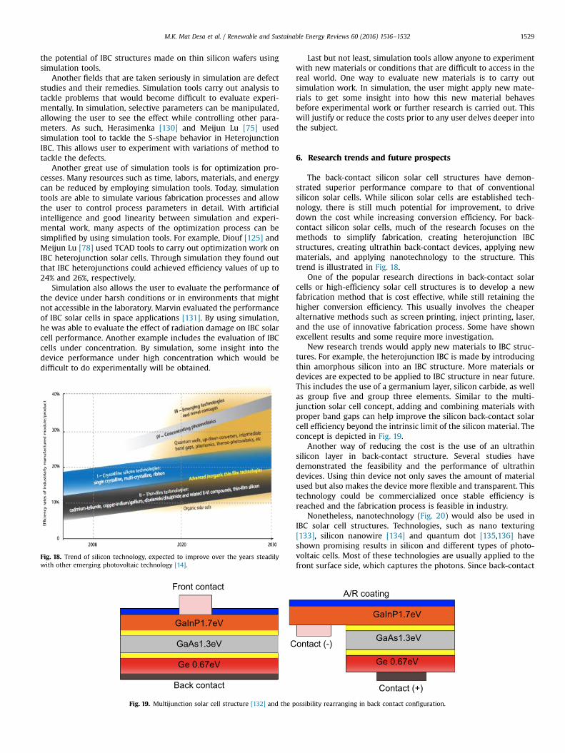
The back-contact silicon solar cell structures have demon-strated superior performance compare to that of conventionalsilicon solar cells. While silicon solar cells are established tech-nology, there is still much potential for improvement, to drivedown the cost while increasing conversion efficiency. For back-contact silicon solar cells, much of the research focuses on themethods to simplify fabrication, creating heterojunction IBCstructures, creating ultrathin back-contact devices, applying newmaterials, and applying nanotechnology to the structure. Thistrend is illustrated in Fig. 18.
One of the popular research directions in back-contact solarcells or high-efficiency solar cell structures is to develop a newfabrication method that is cost effective, while still retaining thehigher conversion efficiency. This usually involves the cheaperalternative methods such as screen printing, inject printing, laser,and the use of innovative fabrication process. Some have shownexcellent results and some require more investigation.
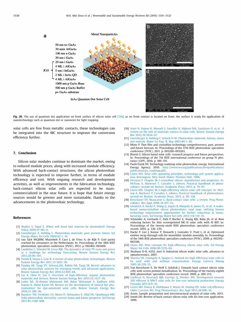
New research trends would apply new materials to IBC struc-tures. For example, the heterojunction IBC is made by introducingthin amorphous silicon into an IBC structure. More materials ordevices are expected to be applied to IBC structure in near future.This includes the use of a germanium layer, silicon carbide, as wellas group five and group three elements. Similar to the multi-junction solar cell concept, adding and combining materials withproper band gaps can help improve the silicon back-contact solarcell efficiency beyond the intrinsic limit of the silicon material. Theconcept is depicted in Fig. 19.
Another way of reducing the cost is the use of an ultrathinsilicon layer in back-contact structure. Several studies havedemonstrated the feasibility and the performance of ultrathindevices. Using thin device not only saves the amount of materialused but also makes the device more flexible and transparent. Thistechnology could be commercialized once stable efficiency isreached and the fabrication process is feasible in industry.
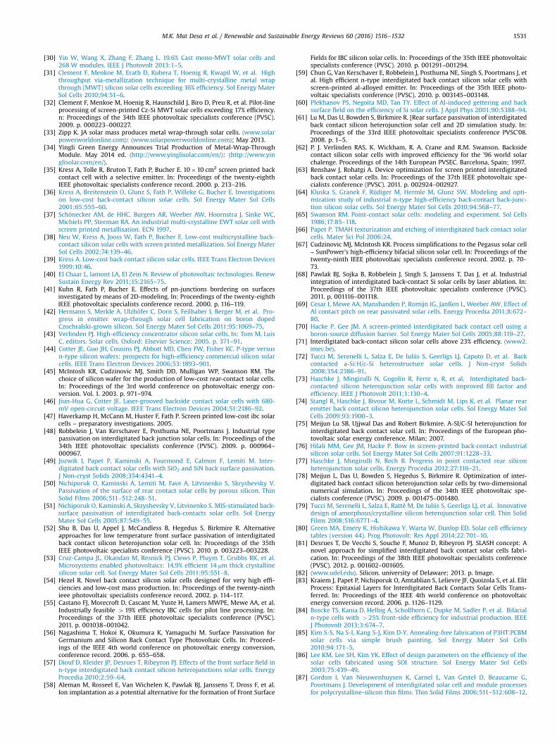
Nonetheless, nanotechnology (Fig. 20) would also be used inIBC solar cell structures. Technologies, such as nano texturing[133], silicon nanowire [134] and quantum dot [135,136] haveshown promising results in silicon and different types of photo-voltaic cells. Most of these technologies are usually applied to thefront surface side, which captures the photons. Since back-contact
ontact (-)
Ge 0.67eV
Contact (+)
GaAs1.3eV
GaInP1.7eV
A/R coating
ossibility rearranging in back contact configuration.
Fig. 20. The use of quantum dot application on front surface of silicon solar cell [136], as no front contact is located on front, the surface is ready for application ofnanotechnology such as quantum dot or nanowire for light trapping.
M.K. Mat Desa et al. / Renewable and Sustainable Energy Reviews 60 (2016) 1516–15321530
solar cells are free from metallic contacts, these technologies canbe integrated into the IBC structure to improve the conversionefficiency further.
7. Conclusion
Silicon solar modules continue to dominate the market, owingto reduced module prices, along with increased module efficiency.With advanced back-contact structures, the silicon photovoltaictechnology is expected to improve further, in terms of moduleefficiency and cost. With ongoing research and developmentactivities, as well as improvements in the fabrication technology,back-contact silicon solar cells are expected to be mass-commercialized in the near future. It is hope that future energysources would be greener and more sustainable, thanks to theadvancements in the photovoltaic technology.
References
[1] Shafiee S, Topal E. When will fossil fuel reserves be diminished? EnergyPolicy 2009;37:181–9.
[2] Goetzberger A, Hebling C. Photovoltaic materials, past, present, future. SolEnergy Mater Sol Cells 2000;62:1–19.
[3] van Sark WGJHM, Muizebelt P, Cace J, de Vries A, de Rijk P. Grid parityreached for consumers in the Netherlands. In: Proceedings of the 38th IEEEphotovoltaic specialists conference (PVSC). 2012. p. 002462–002466.
[4] Candelise C, Winskel M, Gross RJK. The dynamics of solar PV costs and pricesas a challenge for technology forecasting. Renew Sustain Energy Rev2013;26:96–107.
[5] Parida B, Iniyan S, Goic R. A review of solar photovoltaic technologies. RenewSustain Energy Rev 2011;15:1625–36.
[6] Pandey AK, Tyagi VV, Selvaraj JAL, Rahim NA, Tyagi SK. Recent advances insolar photovoltaic systems for emerging trends and advanced applications.Renew Sustain Energy Rev 2016;53:859–84.
[7] Liu X, Chen H, Tan S. Overview of high-efficiency organic photovoltaicmaterials and devices. Renew Sustain Energy Rev 2015;52:1527–38.
[8] Ludin NA, Al-Alwani Mahmoud AM, Bakar Mohamad A, Kadhum AAH,Sopian K, Abdul Karim NS. Review on the development of natural dye pho-tosensitizer for dye-sensitized solar cells. Renew Sustain Energy Rev2014;31:386–96.
[9] Razykov TM, Ferekides CS, Morel D, Stefanakos E, Ullal HS, Upadhyaya HM.Solar photovoltaic electricity: current status and future prospects. Sol Energy2011;85:1580–608.
[10] Asim N, Sopian K, Ahmadi S, Saeedfar K, Alghoul MA, Saadatian O, et al. Areview on the role of materials science in solar cells. Renew Sustain EnergyRev 2012;16:5834–47.
[11] Goetzberger A, Hebling C, Schock H-W. Photovoltaic materials, history, statusand outlook. Mater Sci Eng: R: Rep 2003;40:1–46.
[12] Mints P. Thin film and crystalline technology competitiveness, past, presentand future forecast. In: Proceedings of the 37th IEEE photovoltaic specialistsconference (PVSC). 2011. p. 003260–003263.
[13] Binetti S. Silicon based solar cells: research progress and future perspectives.In: Proceedings of the 7th IEEE international conference on group IV pho-tonics (GFP). 2010. p. 189–191.
[14] Paolo Frank SN. Technology roadmap solar photovoltaic energy. InternationalEnergy Agency; 2010. ⟨http://www.iea.org/publications/freepublications/publication/pv_roadmap.pdf⟩.
[15] Green MA. Solar cells operating principles, technology and system applica-tion. Kensington, New South Wales: Prentice Hall; 1998.
[16] Ferrazza F. Chapter IB-1-crystalline silicon: manufacture and properties. In:McEvoy A, Markvart T, Castañer L, editors. Practical handbook of photo-voltaics. second ed. Boston: Academic Press; 2012. p. 79–97.
[17] Green MA. Chapter IB-2-high-efficiency silicon solar cell concepts. In: McE-voy A, Markvart T, Castañer L, editors. Practical handbook of photovoltaics.second ed. Boston: Academic Press; 2012. p. 99–128.
[18] Kerschaver EV, Beaucarne G. Back-contact solar cells: a review. Prog Photo-voltaics: Res Appl 2006;14:107–23.
[19] Goodrich A, Hacke P, Wang Q, Sopori B, Margolis R, James TL, et al. A wafer-based monocrystalline silicon photovoltaics road map: utilizing knowntechnology improvement opportunities for further reductions in manu-facturing costs. Sol Energy Mater Sol Cells 2013;114:110–35.
[20] Schneider A, Gerhards C, Fath P, Bucher E, Young RJS, Raby JA, et al. Bowreducing factors for thin screenprinted MC-Si solar cells with Al BSF. In:Proceedings of the twenty-ninth IEEE photovoltaic specialists conferencerecord. 2002. p. 336–339.
[21] Hacke P, Gee J, Kumar P, Howarth J, Gonzales V, Pratt L, et al. Optimizedemitter wrap-through cells for monolithic module assembly. In: Proceedingsof the 34th IEEE photovoltaic specialists conference (PVSC). 2009. p. 002102–002106.
[22] Glunz SW. New concepts for high-efficiency silicon solar cells. Sol EnergyMater Sol Cells 2006;90:3276–84.
[23] Neuhaus D-H, #252, nzer A. Industrial silicon wafer solar cells. advances inoptoelectronics. 2007.
[24] Sharma VK, Colangelo A, Spagna G. Outlook for high efficiency solar cells tobe used with and without concentration. Energy Convers Manag1995;36:239–55.
[25] Van Kerschaver E, De Wolf S, Szlufcik J. Towards back contact silicon solarcells with screen printed metallisation. In: Proceedings of the twenty-eighthIEEE photovoltaic specialists conference record. 2000. p. 209–212.
[26] Guillevin N, Heurtault BJB, Geerligs LJ, Weeber AW. Development towards20% efficient Si MWT solar cells for low-cost industrial production. EnergyProcedia 2011;8:9–16.
[27] Green MA, Emery K, Hishikawa Y, Warta W, Dunlop ED. Solar cell efficiencytables (version 40). Prog Photovoltaics: Res Appl 2012;20:606–14.
[28] Azom. Sample preparation and microstructural analysis of solar cells. 2013.[29] Smith DD. Review of back contact silicon solar cells for low-cost application.
M.K. Mat Desa et al. / Renewable and Sustainable Energy Reviews 60 (2016) 1516–1532 1531
[30] Yin W, Wang X, Zhang F, Zhang L. 19.6% Cast mono-MWT solar cells and268 W modules. IEEE J Photovolt 2013:1–5.
[31] Clement F, Menkoe M, Erath D, Kubera T, Hoenig R, Kwapil W, et al. Highthroughput via-metallization technique for multi-crystalline metal wrapthrough (MWT) silicon solar cells exceeding 16% efficiency. Sol Energy MaterSol Cells 2010;94:51–6.
[32] Clement F, Menkoe M, Hoenig R, Haunschild J, Biro D, Preu R, et al. Pilot-lineprocessing of screen-printed Cz-Si MWT solar cells exceeding 17% efficiency.n: Proceedings of the 34th IEEE photovoltaic specialists conference (PVSC).2009. p. 000223–000227.
[33] Zipp K. JA solar mass produces metal wrap-through solar cells. ⟨www.solarpowerworldonline.com⟩: ⟨www.solarpowerworldonline.com⟩; May 2013.
[34] Yingli Green Energy Announces Trial Production of Metal-Wrap-ThroughModule. May 2014 ed. ⟨http://www.yinglisolar.com/en/⟩: ⟨http://www.yinglisolar.com/en/⟩.
[35] Kress A, Tolle R, Bruton T, Fath P, Bucher E. 10�10 cm2 screen printed backcontact cell with a selective emitter. In: Proceedings of the twenty-eighthIEEE photovoltaic specialists conference record. 2000. p. 213–216.
[36] Kress A, Breitenstein O, Glunz S, Fath P, Willeke G, Bucher E. Investigationson low-cost back-contact silicon solar cells. Sol Energy Mater Sol Cells2001;65:555–60.
[37] Schönecker AM, de HHC, Burgers AR, Weeber AW, Hoornstra J, Sinke WC,Michiels PP, Steeman RA. An industrial multi-crystalline EWT solar cell withscreen printed metallisation. ECN 1997.
[38] Neu W, Kress A, Jooss W, Fath P, Bucher E. Low-cost multicrystalline back-contact silicon solar cells with screen printed metallization. Sol Energy MaterSol Cells 2002;74:139–46.
[39] Kress A. Low-cost back contact silicon solar cells. IEEE Trans Electron Devices1999;10:46.
[40] El Chaar L, lamont LA, El Zein N. Review of photovoltaic technologies. RenewSustain Energy Rev 2011;15:2165–75.
[41] Kuhn R, Fath P, Bucher E. Effects of pn-junctions bordering on surfacesinvestigated by means of 2D-modeling. In: Proceedings of the twenty-eighthIEEE photovoltaic specialists conference record. 2000. p. 116–119.
[42] Hermann S, Merkle A, Ulzhöfer C, Dorn S, Feilhaber I, Berger M, et al. Pro-gress in emitter wrap-through solar cell fabrication on boron dopedCzochralski-grown silicon. Sol Energy Mater Sol Cells 2011;95:1069–75.
[43] Verlinden PJ. High-efficiency concentrator silicon solar cells. In: Tom M, LuisC, editors. Solar cells. Oxford: Elsevier Science; 2005. p. 371–91.
[44] Cotter JE, Guo JH, Cousins PJ, Abbott MD, Chen FW, Fisher KC. P-type versusn-type silicon wafers: prospects for high-efficiency commercial silicon solarcells. IEEE Trans Electron Devices 2006;53:1893–901.
[45] McIntosh KR, Cudzinovic MJ, Smith DD, Mulligan WP, Swanson RM. Thechoice of silicon wafer for the production of low-cost rear-contact solar cells.In: Proceedings of the 3rd world conference on photovoltaic energy con-version. Vol. 1. 2003. p. 971–974.
[46] Jiun-Hua G, Cotter JE. Laser-grooved backside contact solar cells with 680-mV open-circuit voltage. IEEE Trans Electron Devices 2004;51:2186–92.
[47] Haverkamp H, McCann M, Huster F, Fath P. Screen printed low-cost ibc solarcells – preparatory investigations. 2005.
[48] Robbelein J, Van Kerschaver E, Posthuma NE, Poortmans J. Industrial typepassivation on interdigitated back junction solar cells. In: Proceedings of the34th IEEE photovoltaic specialists conference (PVSC). 2009. p. 000964–000967.
[49] Jozwik I, Papet P, Kaminski A, Fourmond E, Calmon F, Lemiti M. Inter-digitated back contact solar cells with SiO2 and SiN back surface passivation.J Non-cryst Solids 2008;354:4341–4.
[50] Nichiporuk O, Kaminski A, Lemiti M, Fave A, Litvinenko S, Skryshevsky V.Passivation of the surface of rear contact solar cells by porous silicon. ThinSolid Films 2006;511–512:248–51.
[51] Nichiporuk O, Kaminski A, Skryshevsky V, Litvinenko S. MIS-stimulated back-surface passivation of interdigitated back-contacts solar cells. Sol EnergyMater Sol Cells 2005;87:549–55.
[52] Shu B, Das U, Appel J, McCandless B, Hegedus S, Birkmire R. Alternativeapproaches for low temperature front surface passivation of interdigitatedback contact silicon heterojunction solar cell. In: Proceedings of the 35thIEEE photovoltaic specialists conference (PVSC). 2010. p. 003223–003228.
[53] Cruz-Campa JL, Okandan M, Resnick PJ, Clews P, Pluym T, Grubbs RK, et al.Microsystems enabled photovoltaics: 14.9% efficient 14 μm thick crystallinesilicon solar cell. Sol Energy Mater Sol Cells 2011;95:551–8.
[54] Hezel R. Novel back contact silicon solar cells designed for very high effi-ciencies and low-cost mass production. In: Proceedings of the twenty-ninthieee photovoltaic specialists conference record. 2002. p. 114–117.
[55] Castano FJ, Morecroft D, Cascant M, Yuste H, Lamers MWPE, Mewe AA, et al.Industrially feasible 419% efficiency IBC cells for pilot line processing. In:Proceedings of the 37th IEEE photovoltaic specialists conference (PVSC).2011. p. 001038–001042.
[56] Nagashima T, Hokoi K, Okumura K, Yamaguchi M. Surface Passivation forGermanium and Silicon Back Contact Type Photovoltaic Cells. In: Proceed-ings of the IEEE 4th world conference on photovoltaic energy conversion,conference record. 2006. p. 655–658.
[57] Diouf D, Kleider JP, Desrues T, Ribeyron PJ. Effects of the front surface field inn-type interdigitated back contact silicon heterojunctions solar cells. EnergyProcedia 2010;2:59–64.
[58] Aleman M, Rosseel E, Van Wichelen K, Pawlak BJ, Janssens T, Dross F, et al.Ion implantation as a potential alternative for the formation of Front Surface
Fields for IBC silicon solar cells. In: Proceedings of the 35th IEEE photovoltaicspecialists conference (PVSC). 2010. p. 001291–001294.
[59] Chun G, Van Kerschaver E, Robbelein J, Posthuma NE, Singh S, Poortmans J, etal. High efficient n-type interdigitated back contact silicon solar cells withscreen-printed al-alloyed emitter. In: Proceedings of the 35th IEEE photo-voltaic specialists conference (PVSC). 2010. p. 003145–003148.
[60] Plekhanov PS, Negoita MD, Tan TY. Effect of Al-induced gettering and backsurface field on the efficiency of Si solar cells. J Appl Phys 2001;90:5388–94.
[61] Lu M, Das U, Bowden S, Birkmire R. [Rear surface passivation of interdigitatedback contact silicon heterojunction solar cell and 2D simulation study. In:Proceedings of the 33rd IEEE photovoltaic specialists conference PVSC'08.2008. p. 1–5.
[62] P. J. Verlinden RAS, K. Wickham, R. A. Crane and R.M. Swanson. Backsidecontact silicon solar cells with improved efficiency for the '96 world solarchalenge. Proceedings of the 14th European PVSEC. Barcelona, Spain; 1997.
[63] Renshaw J, Rohatgi A. Device optimization for screen printed interdigitatedback contact solar cells. In: Proceedings of the 37th IEEE photovoltaic spe-cialists conference (PVSC). 2011. p. 002924–002927.
[64] Kluska S, Granek F, Rüdiger M, Hermle M, Glunz SW. Modeling and opti-mization study of industrial n-type high-efficiency back-contact back-junc-tion silicon solar cells. Sol Energy Mater Sol Cells 2010;94:568–77.
[65] Swanson RM. Point-contact solar cells: modeling and experiment. Sol Cells1986;17:85–118.
[66] Papet P. TMAH texturization and etching of interdigitated back contact solarcells. Mater Sci Pol 2006:24.
[67] Cudzinovic MJ, McIntosh KR. Process simplifications to the Pegasus solar cell– SunPower's high-efficiency bifacial silicon solar cell. In: Proceedings of thetwenty-ninth IEEE photovoltaic specialists conference record. 2002. p. 70–73.
[68] Pawlak BJ, Sojka B, Robbelein J, Singh S, Janssens T, Das J, et al. Industrialintegration of interdigitated back-contact Si solar cells by laser ablation. In:Proceedings of the 37th IEEE photovoltaic specialists conference (PVSC).2011. p. 001116–001118.
[69] Cesar I, Mewe AA, Manshanden P, Romijn IG, Janßen L, Weeber AW. Effect ofAl contact pitch on rear passivated solar cells. Energy Procedia 2011;8:672–80.
[70] Hacke P, Gee JM. A screen-printed interdigitated back contact cell using aboron-source diffusion barrier. Sol Energy Mater Sol Cells 2005;88:119–27.
[71] Interdigitated back-contact silicon solar cells above 23% efficiency. ⟨www2.imec.be⟩.
[72] Tucci M, Serenelli L, Salza E, De Iuliis S, Geerligs LJ, Caputo D, et al. Backcontacted a-Si:H/c-Si heterostructure solar cells. J Non-cryst Solids2008;354:2386–91.
[73] Haschke J, Mingirulli N, Gogolin R, Ferre x, R, et al. Interdigitated back-contacted silicon heterojunction solar cells with improved fill factor andefficiency. IEEE J Photovolt 2011;1:130–4.
[74] Stangl R, Haschke J, Bivour M, Korte L, Schmidt M, Lips K, et al. Planar rearemitter back contact silicon heterojunction solar cells. Sol Energy Mater SolCells 2009;93:1900–3.
[75] Meijun Lu SB, Ujjwal Das and Robert Birkmire. A-SI/C-SI heterojunction forinterdigitated back contact solar cell. In: Proceedings of the European pho-tovoltaic solar energy conference. Milan; 2007.
[76] Hilali MM, Gee JM, Hacke P. Bow in screen-printed back-contact industrialsilicon solar cells. Sol Energy Mater Sol Cells 2007;91:1228–33.
[77] Haschke J, Mingirulli N, Rech B. Progress in point contacted rear siliconheterojunction solar cells. Energy Procedia 2012;27:116–21.
[78] Meijun L, Das U, Bowden S, Hegedus S, Birkmire R. Optimization of inter-digitated back contact silicon heterojunction solar cells by two-dimensionalnumerical simulation. In: Proceedings of the 34th IEEE photovoltaic spe-cialists conference (PVSC). 2009. p. 001475–001480.
[79] Tucci M, Serenelli L, Salza E, Rattè M, De Iuliis S, Geerligs LJ, et al. Innovativedesign of amorphous/crystalline silicon heterojunction solar cell. Thin SolidFilms 2008;516:6771–4.
[80] Green MA, Emery K, Hishikawa Y, Warta W, Dunlop ED. Solar cell efficiencytables (version 44). Prog Photovolt: Res Appl 2014;22:701–10.
[81] Desrues T, De Vecchi S, Souche F, Munoz D, Ribeyron PJ. SLASH concept: Anovel approach for simplified interdigitated back contact solar cells fabri-cation. In: Proceedings of the 38th IEEE photovoltaic specialists conference(PVSC). 2012. p. 001602–001605.
[82] ⟨www.udel.edu⟩. Silicon. university of Delaware; 2013. p. Image.[83] Kraiem J, Papet P, Nichiporuk O, Amtablian S, Lelievre JF, Quoizola S, et al. Elit
Process: Epitaxial Layers for Interdigitated Back Contacts Solar Cells Trans-ferred. In: Proceedings of the IEEE 4th world conference on photovoltaicenergy conversion record. 2006. p. 1126–1129.
[84] Boscke TS, Kania D, Helbig A, Schollhorn C, Dupke M, Sadler P, et al. Bifacialn-type cells with 425% front-side efficiency for industrial production. IEEEJ Photovolt 2013;3:674–7.
[85] Kim S-S, Na S-I, Kang S-J, Kim D-Y. Annealing-free fabrication of P3HT:PCBMsolar cells via simple brush painting. Sol Energy Mater Sol Cells2010;94:171–5.
[86] Lee KM, Lee SH, Kim YK. Effect of design parameters on the efficiency of thesolar cells fabricated using SOI structure. Sol Energy Mater Sol Cells2003;75:439–49.
[87] Gordon I, Van Nieuwenhuysen K, Carnel L, Van Gestel D, Beaucarne G,Poortmans J. Development of interdigitated solar cell and module processesfor polycrystalline-silicon thin films. Thin Solid Films 2006;511–512:608–12.
M.K. Mat Desa et al. / Renewable and Sustainable Energy Reviews 60 (2016) 1516–15321532
[88] Yuan H-C, Page MR, Iwaniczko E, Xu Y, Roybal L, Wang Q, et al. Silicon solarcells with front hetero-contact and aluminum alloy back junction: Preprint2008.
[89] Gu X, Yu X, Guo K, Chen L, Wang D, Yang D. Seed-assisted cast quasi-singlecrystalline silicon for photovoltaic application: Towards high efficiency andlow cost silicon solar cells. Sol Energy Mater Sol Cells 2012;101:95–101.
[90] Nara S, Sakaguchi Y. Newly developed multicrystalline silicon wafer withdiffusion length over 250/spl mu/m. In: Proceedings of 3rd world conferenceon photovoltaic energy conversion. Vol. 2. 2003. p. 1483–1485.
[91] Dengyuan S, Jingfeng X, Zhiyan H, Gaofei L, Hongfang W, Haijiao A, et al.Progress in n-type Si solar cell and module technology for high efficiency andlow cost. In: Proceedings of the 38th IEEE photovoltaic specialists conference(PVSC). 2012. p. 003004–003008.
[92] Buchholz F, Wefringhaus E, Schubert G. Metal surface contamination duringphosphorus diffusion. Energy Procedia 2012;27:287–92.
[94] Yu X, Wang P, Li X, Yang D. Thin Czochralski silicon solar cells based on diamondwire sawing technology. Sol Energy Mater Sol Cells 2012;98:337–42.
[95] De Wolf S, Agostinelli G, Allebe, x, C., Van Kerschaver E, et al. Selectivejunction separation techniques for multi-crystalline silicon solar cells. In:Proceedings of the twenty-ninth IEEE photovoltaic specialists conferencerecord. 2002. p. 320–323.
[96] Madou MJ. Fundamentals of microfabrication the science of miniaturization.United States of America: CRC Press LLC; 2002.
[97] Salami J, Cruz B, Shaikh A. Diffusion paste development for printable IBC andbifacial silicon solar cells. In: Proceedings of the IEEE 4th world conferenceon photovoltaic energy conversion record. 2006. p. 1323–1325.
[98] Guo J-H, Cotter JE. Metallization improvement on fabrication of inter-digitated backside and double sided buried contact solar cells. Sol EnergyMater Sol Cells 2005;86:485–98.
[99] Baraona CRP, OH), Mazaris GAB, OH), Chai A-tNR, OH). Screen printedinterdigitated back contact solar cell. The United States of America asrepresented by the Administrator of the (Washington, DC); 1984.
[100] Jia C, Tey ZHJ, Zhe Ren D, Fen L, Hoex B, Aberle AG. Investigation of screen-printed rear contacts for aluminum local back surface field silicon wafer solarcells. IEEE J Photovolt 2013;3:690–6.
[101] Krause J, Woehl R, Rauer M, Schmiga C, Wilde J, Biro D. Microstructural andelectrical properties of different-sized aluminum-alloyed contacts and theirlayer system on silicon surfaces. Sol Energy Mater Sol Cells 2011;95:2151–60.
[102] Sopori B, Mehta V, Rupnowski P, Moutinho H, Shaikh A, Khadilkar C, et al.Studies on backside Al-contact formation in Si solar cells: fundamentalmechanisms; Preprint. 2009.
[103] Ebong A, Upadhyaya V, Rounsaville B, Kim DS, Meemongkolkiat V, Rohatgi A,et al. Rapid thermal processing of high efficiency n-type silicon solar cellswith al back junction. In: Proceedings of the IEEE 4th world conference onphotovoltaic energy conversion record. 2006. p. 1376–1379.
[104] Chun G, Van Kerschaver E, Robbelein J, Janssens T, Posthuma N, Poortmans J,et al. Screen-printed aluminum-alloyed emitter on high-efficiency n-typeinterdigitated back-contact silicon solar cells. IEEE Electron Device Lett2010;31:576–8.
[105] Granek F. High efficiency back contact back junction silicon solar cells.Freiburg University; 2009. ⟨https://www.freidok.uni-freiburg.de/data/7372⟩.
[106] Sidhu R, Bennett M, Hmung G, Wensheng R, Lian Z, Carlson D, et al. Inter-digitated back contact silicon solar cells with laser fired contacts. In: Pro-ceedings of the IEEE 39th photovoltaic specialists conference (PVSC). 2013. p.1298–1300.
[107] Meier DLD, HP, Shibata A, Abe T, Kinoshita K, Bishop C, Mahajan S, RohatgiAjeet, Doshi P, Finnegan M. Self-doping contacts and associated silicon solarcell structures. In: Proceedings of the 2nd world conference on photovoltaicsolar energy conversion. Vienna, Austria: Georgia Institute of Technology;1998.
[108] Rohatgi AH, Mohamed M, Meier DL, Ebong Abasifreke, Honsberg ChristianaB, Carroll AF, Hacke P. Self-aligned self-doping selective emitter for screen-printed silicon solar cells. In: Proceedings of the 17th European photovoltaicsolar energy conference and exhibition. Munich, Germany: Georgia Instituteof Technology; 2001-10.
[109] Sinton RA, Swanson RM. Simplified backside-contact solar cells. IEEETrans Electron Devices 1990;37:348–52.
[110] Verlinden P, Lafontaine B, Jacquemin P, Goutain E, Crahay A. Super self-aligned technology for backside contact solar cells. A route to low cost andhigh efficiency. In: Proceedings of the twenty-first IEEE photovoltaic specia-lists conference record. Vol. 1. 1990. p. 257–262.
[111] Itoh U, Yoshida M, Tokuhisa H, Ushifusa N, Sumita I, Fukunishi T, et al. Screenprinted finger electrode with high aspect ratio by single printing for crystal Si
solar cell using novel screen mask. In: Proceedings of the 38th IEEE photo-voltaic specialists conference (PVSC). 2012. p. 002167–002170.
[112] Ju M, Lee Y-J, Lee J, Kim B, Ryu K, Choi K, et al. Double screen printedmetallization of crystalline silicon solar cells as low as 30 μmmetal line widthfor mass production. Sol Energy Mater Sol Cells 2012;100:204–8.
[113] Kröner F, Kröner Z, Reichmann K, Rommel M. All electrochemical layerdeposition for crystalline silicon solar cell manufacturing: experiments andinterpretation. Sol Energy 2012;86:548–57.
[114] Chaudhari VA, Solanki CS. A novel two step metallization of Ni/Cu for lowconcentrator c-Si solar cells. Sol Energy Mater Sol Cells 2010;94:2094–101.
[115] Silva JA, Gauthier M, Boulord C, Oliver C, Kaminski A, Semmache B, et al.Progress in the metallisation of n-type multicrystalline silicon solar cells. SolEnergy Mater Sol Cells 2011;95:3333–40.
[116] Kalio A, Richter A, Hörteis M, Glunz SW. Metallization of n-type silicon solarcells using fine line printing techniques. Energy Procedia 2011;8:571–6.
[117] Nejati M, Wen Z, Lun H. Etching paste for innovative solar-cell applications.IEEE J Photovolt 2013;3:669–73.
[118] Mishra R, Zhao L, Zhang Z, Guo HW, Kumar P, Mungekar H, et al. Develop-ment of no-rinse screen printable etch paste for contact via in dielectric films.In: Proceedings of the 35th IEEE photovoltaic specialists conference (PVSC).2010. p. 003536–003539.
[119] Ebong A, Nian C. Metallization of crystalline silicon solar cells: a review. In:Proceedings of the 9th international conference on high capacity opticalnetworks and enabling technologies (HONET). 2012. p. 102–109.
[120] Haug H, Olaisen BR, Nordseth Ø, Marstein ES. A graphical user interface formultivariable analysis of silicon solar cells using scripted PC1D simulations.Energy Procedia 2013;38:72–9.
[121] Boussettine AA, Belhadji Y, Benmansour A. Modeling of Tandem solar cella-Si/a-SiGe using AMPS-1D program. Energy Procedia 2012;18:693–700.
[122] Verschraegen J, Burgelman M. Numerical modeling of intra-band tunnelingfor heterojunction solar cells in scaps. Thin Solid Films 2007;515:6276–9.
[123] Froitzheim A, Stangl R, Elstner L, Kriegel M, Fuhs W. AFORS-HET: a computer-program for the simulation of heterojunction solar cells to be distributed forpublic use. In: Proceedings of 3rd world conference on photovoltaic energyconversion. Vol. 1. 2003. p. 279–282.
[124] Koduvelikulathu VDM LJ, Galbiati G, Halm A, Roescu R, Kopecek R, Peter K. 2-D modelling of n-type ibc solar cells using silvaco atlas simulation. In: Pro-ceedings of the 11th international conference on numerical simulation ofoptoelectronic devices. Rome, Italy; 2011.
[125] Diouf D, Kleider JP, Desrues T, Ribeyron PJ. Study of interdigitated backcontact silicon heterojunctions solar cells by two-dimensional numericalsimulations. Mater Sci Eng: B 2009;159–160:291–4.
[126] Daliento S, Lancellotti L. 3D Analysis of the performances degradation causedby series resistance in concentrator solar cells. Sol Energy 2010;84:44–50.
[127] Nichiporuk O, Kaminski A, Lemiti M, Fave A, Skryshevsky V. Optimisation ofinterdigitated back contacts solar cells by two-dimensional numericalsimulation. Sol Energy Mater Sol Cells 2005;86:517–26.
[129] Kim DS, Meemongkolkiat V, Ebong A, Rounsaville B, Upadhyaya V, Das A, etal. 2D-modeling and development of interdigitated back contact solar cellson low-cost substrates. In: Proceedings of the IEEE 4th world conference onphotovoltaic energy conversion record. 2006. p. 1417–1420.
[130] Herasimenka S, Ghosh K, Bowden S, Honsberg C. 2D modeling of siliconheterojunction interdigitated back contact solar cells. In: Proceedings of the35th IEEE photovoltaic specialists conference (PVSC). 2010. p. 001390–001394.
[131] Marvin DC, Froedge SL. Analysis of interdigitated back contact silicon solarcells for space use. In: Proceedings of the Proceedings of the 24th intersocietyenergy conversion engineering conference IECEC-89. Vol. 2. 1989. p. 821–827.
[132] King RR, Law DC, Edmondson KM, Fetzer CM, Kinsey GS, Yoon H, et al. 40%efficient metamorphic multijunction solar cells. Appl Phys Lett 2007;90(183516):3.
[133] Repo P, Benick J, Vähänissi V, Schön J, von Gastrow G, Steinhauser B, et al. N-type black silicon solar cells. Energy Procedia 2013;38:866–71.
[134] Huang B-R, Yang Y-K, Lin T-C, Yang W-L. A simple and low-cost technique forsilicon nanowire arrays based solar cells. Sol Energy Mater Sol Cells2012;98:357–62.
[135] Pi X, Li Q, Li D, Yang D. Spin-coating silicon-quantum-dot ink to improve solarcell efficiency. Sol Energy Mater Sol Cells 2011;95:2941–5.
[136] Wu J, Mangham SC, Reddy VR, Manasreh MO, Weaver BD. Surface plasmonenhanced intermediate band based quantum dots solar cell. Sol Energy MaterSol Cells 2012;102:44–9.