Hindawi Publishing CorporationISRN NanomaterialsVolume 2013, Article ID 132798, 5 pageshttp://dx.doi.org/10.1155/2013/132798
Research ArticleFabrication of Aluminium Nanowires byDifferential Pressure Injection
A. Hashoosh,1 H. Hirshy,2 E. B. Brousseau,2 and A. Moosa3
1 Department of Materials Engineering, The University of Technology, Baghdad, Iraq2 Cardiff School of Engineering, Cardiff University, Cardiff CF24 3AA, UK3Department of Materials Engineering, Technical College—Baghdad, Baghdad, Iraq
The reported study aims to demonstrate the application of a simple technique, which is referred to as pressure differential injection,to prepare metallic nanowires. This technique relies on the difference in pressure between the inside of sealed nanochannels ofan anodic aluminium oxide (AAO) substrate and the ambient atmosphere to inject a molten metal, which is previously depositedon the substrate, into the AAO pores. The application of this technique enabled the fabrication of nanowires in aluminium withdiameters comprised between 55 nm and 65 nm.
1. Introduction
Among the different structures, which have contributed tothe advent of the field of nanotechnology, metallic nanowireshave played an important role as these one-dimensional com-ponents typically exhibit very different physical properties incomparison to their bulk counterparts due to quantum con-finement effects. Such characteristics are of specific interest tomeet the demand for the development of future miniaturisedsystems such as electronic and optical devices. In particular,nanowires in aluminium represent a potential candidatetechnology for the development of high-density and high-resolutionmicroelectronic systems and future energy storagedevices [1]. Aluminium has the benefits of low melting point,chemical stability, ductility, good electrical conductivity, andreasonable cost.
However, in order to enable further studies of theproperties of such nanostructures as well as their scaled-up deployment in potential applications, it is important toensure that their production can be carried out efficiently,reliably, and cost effectively. A number of techniques havebeen investigated for the synthesis of nanowires such aselectrodeposition [2] and chemical vapour deposition [3].While these fabrication processes enable the manufacture of
nanowires in different materials, they have been reported toshow a lack of reliability over the control of the uniformityand the length of the produced nanowires [4]. To overcomethese issues, the pressure injection method has been utilisedsuccessfully to form nanowires in various metals such asbismuth (Bi) [4], tin (Sn) [5], and Al [6]. This method relieson injecting a molten metal into the pores of an anodicaluminium oxide (AAO) substrate. In order to fill the AAOchannels, external pressure is required for overcoming thesurface tension of the molten metal. The necessary pressurecan be described by the well-known Washburn equation,which is expressed as follows:
𝑃 = −4𝛾 cos 𝜃𝐷, (1)
where 𝐷 is the pore diameter of the AAO substrate used,𝛾 is the surface tension of the metallic melt, and 𝜃 is thecontact angle between the template and the molten metal.For a given melt, the applied pressure needed is relativelyhigh, and it increases as the size of the pores decreases. Forexample, in the case of Sn nanowires, 350 bar and 1400 barare, respectively, required for pore diameter of 60 nm and15 nm [5]. In this study, the surface tension of Al is taken as
2 ISRN Nanomaterials
0
2
4
6
8
10
12
14
0 20 40 60 80 100
Requ
ired
pres
sure
(kba
r)
AAO pore diameter (nm)
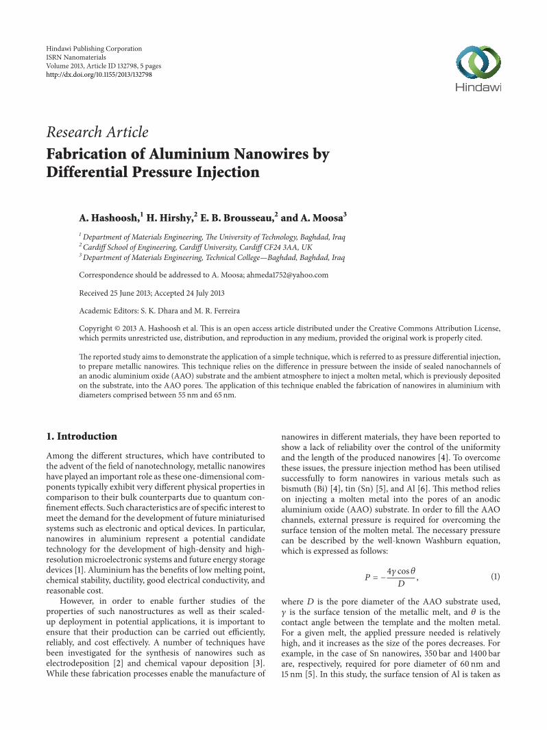
Figure 1: Estimated evolution of the required pressure to fill AAOchannels withAlmelt as a function of the pore diameter for a contactangle 𝜃 = 180∘.
𝛾 = 0.914N/m [7] and the contact angle, 𝜃, is considered tobe equal to 180∘, which represents a conservative value andwill give the upper limit for the pressure required. In this way,the evolution of the necessary pressure to be applied to injectmolten aluminium could be estimated as a function of thediameter of the AAO pores as shown in Figure 1.
To reach such a high pressure range during the nanowireinjection process, two main methods have been utilized,namely, gas injection and vacuum hydraulic pressure injec-tion. The gas-assisted injection technique has been usedto manufacture bismuth-antimony (Bi-Sb) alloy nanowires45 nm in diameter [8], tellurium- (Te-) doped Bi nanowires40 nm in diameter [9], and Bi nanowires as small as 13 nmin diameter [10]. The vacuum hydraulic pressure injectiontechnique has been proposed as a simple alternative to thegas-assisted method in order to achieve a higher range ofapplied pressure values. Sn nanowires with diameter as smallas 15 nm [5] as well as Bi nanowires [4] were fabricated withthis method. In addition, researchers also investigated theimplementation of centrifugal forces applied in vacuum forinjecting a lead- (Pb-) Bi melt into the channels of an AAOsubstrate, which led to the production of Pb-Bi nanowireswith a diameter of 80 nm [11]. Sung and coworkers describedanother alternative injection technique to fill the pores ofan AAO substrate, which does not require gas or hydraulicpressure [12]. In particular, the technique consists of usingthermal evaporation under vacuum first in order to deposita thin metallic layer, a few hundreds nm thick, onto theAAO substrate, and then this is followed by heating the filmand AAO template above the melting point of the depositedmetal under atmospheric pressure. Thus, the injection of themelt into the pores relies on the pressure differential betweenthe outside ambient pressure and the inside of the AAOchannels, which are sealed by the metallic film as a resultof the thermal evaporation process. Although the techniquedescribed by Sung and coworkers led to the fabrication ofaluminium nanotubes, the authors believe that by adjustingthe process parameters, it could also be used as a simpleand cost-effective alternative to existing pressure injectionmethods for synthesising Al nanowires. Based on the datashown in Figure 1, a pressure differential below 10 kbar is
required to fill melted Al into AAO pores with dimensions of5 nmand above.Thus, if the value of the atmospheric pressureis taken as 1 bar, then the vacuum required during the initialevaporation process is of 0.1mbar, which is easily achieved byvacuum systems.
In this context, the objective of this study is to demon-strate that the pressure differential method can also beemployed to prepare Al nanowires by suitably controlling theprocess parameters, namely, the metallic film thickness andthe heating time during the injection phase of the process.The remaining part of the paper is organised as follows. Thenext section presents the experimental procedure used toprepare AAO substrates with varying pores dimensions.Thissection also describes the experimental technique followedto deposit Al on the AAO templates as well as the methodemployed to inject Al into the AAO pores. Then, the resultsobtained are presented, and finally the conclusions reachedand perspectives for future work are given.
2. Experimental Procedure
2.1. Fabrication of the AAO Templates. The AAO substrateswere fabricated using the two-step anodization process.In particular, Al foils with dimensions 30mm × 20mm ×0.15mmand 99%purity were annealed in an electric furnace.Prior to and following the annealing, the foils were cleanedin an ultrasonic bath with acetone for 5 minutes. Next, theAl samples were treated with a sodium hydroxide (NaOH)solution for 2 minutes in order to remove the oxide layerproduced during the annealing step. The samples were thenwashed with deionized (DI) water before being chemicallypolished in a solution comprised of 3.5mL phosphoric acid(H3PO4) and 4.5 g of chromium trioxide (CrO
3) dissolved
in 96.5mL of water. This polishing step was conducted at80∘C for 10 minutes. The cleaned and polished Al sampleswere then anodized at 40V in 0.3M oxalic acid for 1 hourusing a stainless steel sheet as the cathode. Three sampleswere produced in this way at the respective temperature of17∘C, 19∘C, and 25∘C in order to study the influence of thetemperature applied during the first anodizing step on theresulting pore diameters. In order to keep the temperatureconstant during this step, the anodizing cell was cooled ina bath of liquid monoethylene for which the temperaturewas controlled with a chiller and monitored with a K-typethermocouple. Following this, the aluminium oxide porousfilm formed was stripped off using a solution of H
3PO4
(8.75mL), CrO3(5 g), and water (241.25mL) at 50∘C for 10
minutes. The samples were then washed in DI water anddried.The purpose of this first anodization step is to generateperiodic concave hexagonal structures on the Al substratewhich can act as the seed pattern for the second anodization.This second step was conducted under the same conditionsas the first anodization with the exception that it lasted for 11hours. Following this, the samples were washed in DI water,and a pore widening treatment was conducted by immersingthe samples in a solution of H
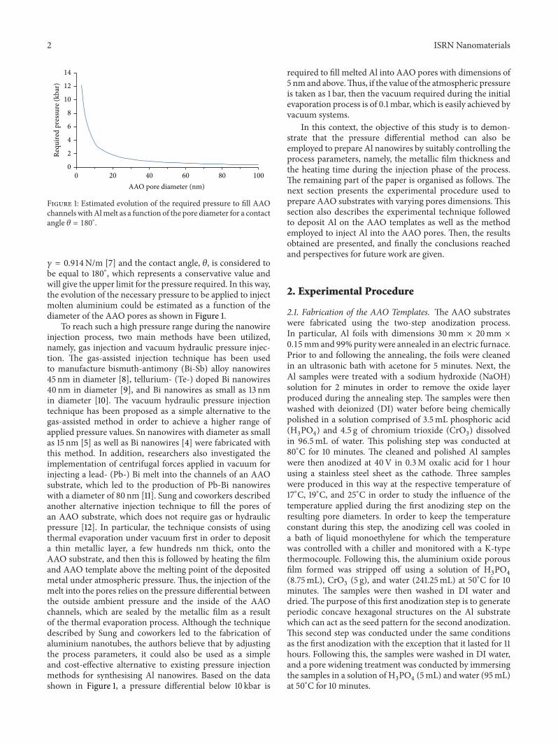
Figure 2: AFM scan of the AAO sample processed at 19∘C.
2.2. Fabrication of Al Nanowires by Differential Pressure Injec-tion. An electron beam (e-beam) evaporation system fromEdwards (type Auto 500) was used to deposit the aluminiumfilm on top of the surface of the AAO samples. Table 1summarises the parameters used during this evaporationprocess. In particular, the evaporation pressure utilised was4⋅10−6mbar, which is well above the pressure required for the
injection of the Al melt as calculated in the previous section.Following this deposition step, the AAO substrates wereplaced in an electric furnace at 700∘C, which was just abovethe melting point of Al (660∘C), for 50 s under atmosphericpressure.
The final step consisted in dissolving the AAO substratesin order to reveal the nanowires. For this, a solution of sodiumhydroxide with a concentration of 5 g NaOH+ and 100mL ofwater was used for 10minutes.The samples were then washedin deionized water.
2.3. Characterisation Techniques. An atomic force micro-scope (AFM) from Angstrom Advanced (type CSPM-AA3000) was used in noncontact mode to inspect qualita-tively the surface of the AAO samples prepared. Figure 2shows an example of an AFM scan obtained for the sampleanodized at a temperature of 19∘C. In addition, a dual focusedion beam (FIB) and scanning electron microscope (SEM)system from Carl Zeiss (type XB1540) were utilised for thecomplementary quantitative analysis of the AAO samples. Inparticular, the SEMmicrographs obtained were used to mea-sure the pores diameters and the interpore distance, while theFIB was employed to mill the surface of the AAO specimenand thus to reveal their cross-sections.The thickness of the Alfilm deposited prior to the injection step was measured usinga Dektak surface profiler. Finally, X-ray diffraction (XRD)
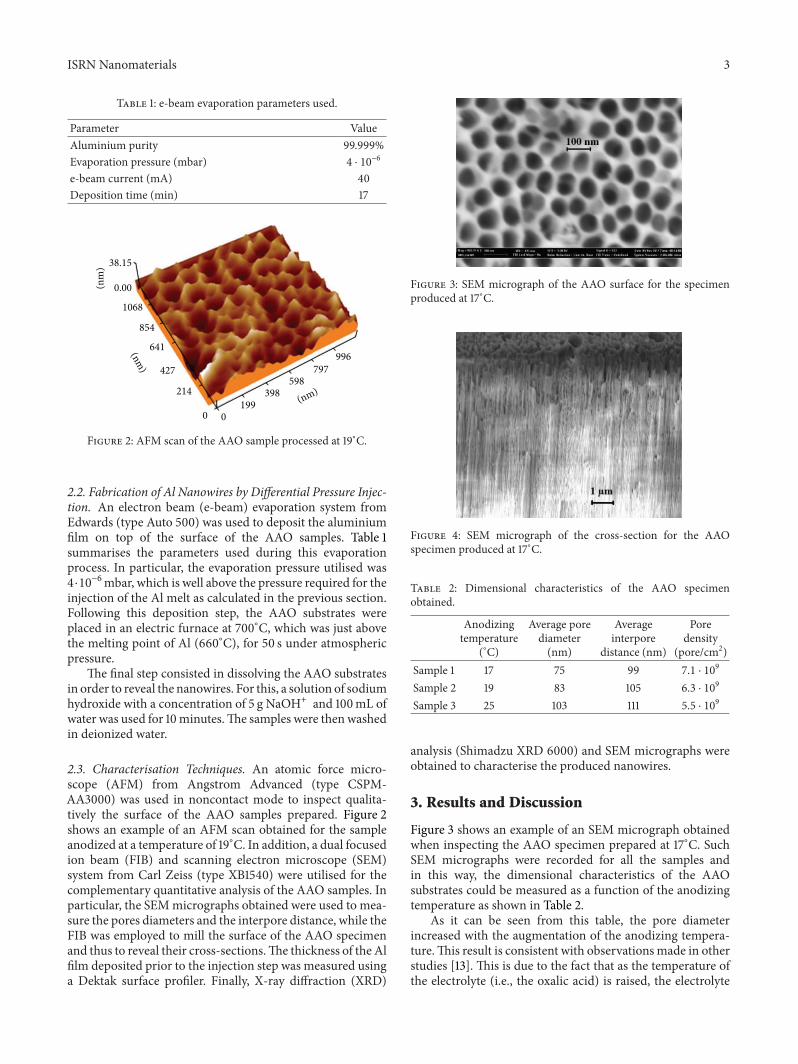
Figure 3: SEM micrograph of the AAO surface for the specimenproduced at 17∘C.
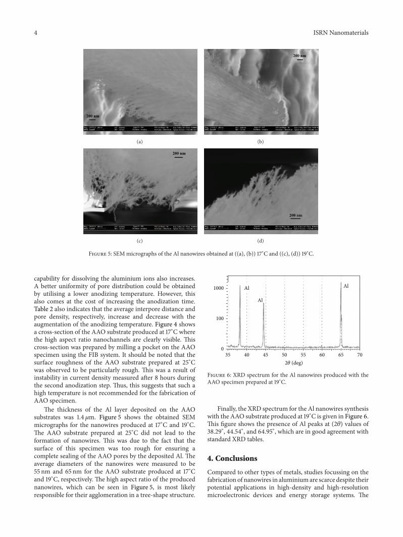
Figure 4: SEM micrograph of the cross-section for the AAOspecimen produced at 17∘C.
Table 2: Dimensional characteristics of the AAO specimenobtained.
Anodizingtemperature
(∘C)
Average porediameter(nm)
Averageinterpore
distance (nm)
Poredensity
(pore/cm2)Sample 1 17 75 99 7.1 ⋅ 10
9
Sample 2 19 83 105 6.3 ⋅ 109
Sample 3 25 103 111 5.5 ⋅ 109
analysis (Shimadzu XRD 6000) and SEM micrographs wereobtained to characterise the produced nanowires.
3. Results and Discussion
Figure 3 shows an example of an SEM micrograph obtainedwhen inspecting the AAO specimen prepared at 17∘C. SuchSEM micrographs were recorded for all the samples andin this way, the dimensional characteristics of the AAOsubstrates could be measured as a function of the anodizingtemperature as shown in Table 2.
As it can be seen from this table, the pore diameterincreased with the augmentation of the anodizing tempera-ture.This result is consistent with observationsmade in otherstudies [13]. This is due to the fact that as the temperature ofthe electrolyte (i.e., the oxalic acid) is raised, the electrolyte
4 ISRN Nanomaterials
(a) (b)
(c) (d)
Figure 5: SEM micrographs of the Al nanowires obtained at ((a), (b)) 17∘C and ((c), (d)) 19∘C.
capability for dissolving the aluminium ions also increases.A better uniformity of pore distribution could be obtainedby utilising a lower anodizing temperature. However, thisalso comes at the cost of increasing the anodization time.Table 2 also indicates that the average interpore distance andpore density, respectively, increase and decrease with theaugmentation of the anodizing temperature. Figure 4 showsa cross-section of the AAO substrate produced at 17∘C wherethe high aspect ratio nanochannels are clearly visible. Thiscross-section was prepared by milling a pocket on the AAOspecimen using the FIB system. It should be noted that thesurface roughness of the AAO substrate prepared at 25∘Cwas observed to be particularly rough. This was a result ofinstability in current density measured after 8 hours duringthe second anodization step. Thus, this suggests that such ahigh temperature is not recommended for the fabrication ofAAO specimen.
The thickness of the Al layer deposited on the AAOsubstrates was 1.4𝜇m. Figure 5 shows the obtained SEMmicrographs for the nanowires produced at 17∘C and 19∘C.The AAO substrate prepared at 25∘C did not lead to theformation of nanowires. This was due to the fact that thesurface of this specimen was too rough for ensuring acomplete sealing of the AAO pores by the deposited Al. Theaverage diameters of the nanowires were measured to be55 nm and 65 nm for the AAO substrate produced at 17∘Cand 19∘C, respectively. The high aspect ratio of the producednanowires, which can be seen in Figure 5, is most likelyresponsible for their agglomeration in a tree-shape structure.
35 40 45 50 55 60 65 702𝜃 (deg)
0
100
1000 Al Al
Al
Figure 6: XRD spectrum for the Al nanowires produced with theAAO specimen prepared at 19∘C.
Finally, the XRD spectrum for the Al nanowires synthesiswith the AAO substrate produced at 19∘C is given in Figure 6.This figure shows the presence of Al peaks at (2𝜃) values of38.29∘, 44.54∘, and 64.95∘, which are in good agreement withstandard XRD tables.
4. Conclusions
Compared to other types of metals, studies focussing on thefabrication of nanowires in aluminiumare scarce despite theirpotential applications in high-density and high-resolutionmicroelectronic devices and energy storage systems. The
ISRN Nanomaterials 5
research reported here demonstrated that it is possible touse a simple technique that relies on the pressure differentialbetween the inside of the nanochannels of an AAO substrateand the ambient atmosphere to inject molten Al into theAAO pores. This technique had been investigated previouslyon one occasion for the formation of Al nanotubes andreferred to as “two-step evaporation method.” However, inthe case of the study reported here, the technique is moreaccurately described by the term “differential pressure injec-tion method.” In particular, the authors do not believe thatevaporation plays a role in filling the AAO pores during theinjection process given that the temperature used for this stepis just above the melting point of the injected metal. In orderto use the technique successfully, this study suggests that it isimportant to ensure a complete sealing of theAAOnanoporesthrough the evaporation of Al prior to the injection step.However, attention must be paid to ensure that a high levelof surface finish is achieved first on the surface of the AAOsamples. Thus, future work should focus on this particularaspect as well as on the systematic study of the influence of theapplied injection parameters, such as the thickness of themeltand the heating time and temperature, on the characteristicsof the synthetized nanowires.
Acknowledgment
The authors are greatly indebted to the Iraqi Ministry ofHigher Education and Scientific Research for supporting thisstudy.
References
[1] J. Benson, S. Boukhalfa, A. Magasinski, A. Kvit, and G. Yushin,“Chemical vapor deposition of aluminum nanowires on metalsubstrates for electrical energy storage applications,”ACS Nano,vol. 6, no. 1, pp. 118–125, 2012.
[2] S. Michotte, S. Matefi-Tempfli, and L. Piraux, “Current-voltage characteristics of Pb and Sn granular superconductingnanowires,” Applied Physics Letters, vol. 82, no. 23, Article ID4119, 3 pages, 2003.
[3] G. S. Cheng, L. D. Zhang, S. H. Chen et al., “Ordered nanos-tructure of single-crystalline GaN nanowires in a honeycombstructure of anodic alumina,” Journal of Materials Research, vol.15, no. 2, pp. 347–350, 2000.
[4] Y. Bisrat, Z. P. Luo, D. Davis, and D. Lagoudas, “Highlyordered uniform single-crystal Bi nanowires: fabrication andcharacterization,” Nanotechnology, vol. 18, no. 39, Article ID395601, 2007.
[5] C. Chen, Y. Bisrat, Z. P. Luo, R. E. Schaak, C.-G. Chao, andD. C. Lagoudas, “Fabrication of single-crystal tin nanowires byhydraulic pressure injection,” Nanotechnology, vol. 17, no. 2, pp.367–374, 2006.
[6] C. A. Huber, T. E. Huber, M. Sadoqi, J. A. Lubin, S. Manalis, andC. B. Prater, “Nanowire array composites,” Science, vol. 263, no.5148, pp. 800–802, 1994.
[7] C. J. Smithells and E. A. Brandes, Metals Reference Book,Butterworth-Heinemann, New York, NY, USA, 5fth edition,1976.
[8] Y. Lin, S. B. Cronin, O. Rabin, J. Y. Ying, and M. S. Dresselhaus,“Transport properties of Bi1-x-Sbx alloy nanowires synthesized
[9] Y. M. Lin, X. Sun, S. B. Cronin, Z. Zhang, J. Y. Ying, and M.S. Dresselhaus, “Fabrication, transport properties of Te-dopedBi nanowire arrays,” in Proceedings of the Materials ResearchSociety Fall Meeting, vol. 582, no. 1–6, pp. H10–H13, Boston,Mass, USA, December 1999.
[10] Z. Zhang, J. Y. Ying, andM. S. Dresselhaus, “Bismuth quantum-wire arrays fabricated by a vacuum melting and pressureinjection process,” Journal of Materials Research, vol. 13, no. 7,pp. 1745–1748, 1998.
[11] C. G. Kuo and C. G. Chao, “A novel method of centrifugalprocessing for the synthesis of lead-bismuth eutectic alloynanospheres and nanowires,” The International Journal ofAdvanced Manufacturing Technology, vol. 32, no. 5-6, pp. 468–472, 2007.
[12] D. D. Sung, M. S. Choo, J. S. Noh, W. B. Chin, and W. S.Yang, “A new fabrication method of aluminum nanotube usinganodic porous alumina film as a template,”Bulletin of the KoreanChemical Society, vol. 27, no. 8, pp. 1159–1163, 2006.
[13] G. D. Sulka and W. J. Stepniowski, “Structural features of self-organized nanopore arrays formed by anodization of aluminumin oxalic acid at relatively high temperatures,” ElectrochimicaActa, vol. 54, no. 14, pp. 3683–3691, 2009.


![Matter of [REDACTED], ID# 13768 (AAO Mar. 15, 2017) REGIONAL CENTER TERMINATION AAO REMAND](https://static.documents.pub/doc/80x56/58d1015e1a28abc00b8b715f/matter-of-redacted-id-13768-aao-mar-15-2017-regional-center-termination.jpg)


