Hindawi Publishing CorporationInternational Journal of OpticsVolume 2012, Article ID 130517, 17 pagesdoi:10.1155/2012/130517
Research Article
Light Combining for Interferometric Switching
Marco Masi,1 Mattia Mancinelli,2 Paolo Bettotti,2 and Lorenzo Pavesi2
1 Institut des Nanotechnologies de Lyon, Universite de Lyon, INL-UMR5270, CNRS, INSA de Lyon, 69621 Villeurbanne, France2 Nanoscience Laboratory, Department of Physics, University of Trento, Via Sommarive 14, 38121 Trento, Italy
Interferometric switching as a routing method in sequence of coupled optical microresonators is explored. Mach-Zhenderinterferometry is extended to systems of side-coupled integrated sequences of resonators (SCISSORs) and coupled resonatorsoptical waveguides (CROWs). We generalized Coupled Mode Theory (CMT) to a system of three coupled waveguides. The twobus interferometric switching functions of SCISSOR and CROW resonant structures are investigated. A novel switching devicebased on three input phase modulation ports is presented. This device displays a wide range of switching behaviors which mightlead to new interesting applications.
1. Introduction
The tremendous growth of communication services andinformation technologies demands new and enhanced net-working capabilities. Switching is one of the main functionsof communication systems and networks. In particular, noveloptical switching technologies have the potential to play adecisive role in future telecommunication and informationprocessing systems. The extensive deployment of wavelengthdivision multiplexing (WDM) technologies demands forhigh-speed, scalable, and rapidly reconfigurable networkswitching. Several optical switching technologies exist, likeelectrooptic (EO), acoustooptic (AO), thermooptic (TO),optomechanical (OM), and optical amplifier (OA) basedswitching. Refractive index modulation, inducing phase dif-ferences for switching functionalities, resorts especially toEO or TO effects. These are widely used in directionalcouplers, Mach-Zehnder interferometers, and multi-modeinterference (MMI) switches (for a good review see, e.g.,[1]). The present paper focuses on some possible extensionsof these interferometric techniques by means of sequencesof microoptical resonator systems, like SCISSORs (side-coupled integrated spaced-sequences of resonators) andCROWs (coupled resonator optical waveguides) [2–6]. Aparticular combination of these allows to use three inputwaveguides for amplitude and phase modulation. The
advantage of a system of resonators over conventional single-resonator scheme coupling is its larger spectral band, thepossibility to operate through interferometry on severalchannels and its higher design flexibility. In particular, thislatter aspect allows for a diversity of behaviors compared tousual directional coupling switching.
The practical realization of such kind of phase switchingdevices is, however, still limited by present photonic fabri-cation tolerances. Phase shifting of light requires the sameinterferometric precision as the device operation itself. Forexample, the phase difference between two interfering lightbeams needs to be tightly controlled at the subwavelengthlevel to provide efficient switching. Even more sensitive tosmall deviations from the nominal parameters are deviceswhere coherent addition of signals is achieved by arrangingcomplex systems of resonator chains. These require nanome-ter level accuracy in the fabrication of the single resonatorsand their mutual spacings. For instance, coupled resonatorinduced transparency (CRIT) effects emerge easily only forfew nanometer deviations [7–12]. However, while presentoptical lithography still suffers of few nanometers impre-cision needing further improvements, the next generationoptical lithography is likely to achieve an order of magnitudeleap in accuracy paving the way to novel interferometricdevices [13]. Also, the fabrication of electrooptic silicon-photonic modulators which are capable of providing smooth
2 International Journal of Optics
and uniform phase shifts over a broad spectrum is a topicof intense research and promises to find a wide area ofapplications [14]. Elsewhere we have demonstrated the prac-tical realization of a novel silicon photonic interferometricswitching device showing that resonator phase switching isindeed feasible [12]. Therefore, it is interesting to explorefrom the theoretical point of view some extensions ofconventional directional coupling methods which could havepotential applications in upcoming interferometric devices.
The next section will briefly summarize the basics of cou-pled mode theory (CMT) which will be particularly useful inour context. Section 2 will set the stage for interferometricswitching between three waveguides which in turn will beused in Section 3 where interferometric switching with adual bus waveguide resonator system is described. Section 4will extend this to a particular arrangement of three-busresonator systems.
2. CMT and Phase Switching forthe Double-Sided SymmetricCodirectional Coupler
CMT has grown to a vast subject in the last three decades (fora good introduction see e.g., [15]). Let us quickly recall somestandard equations which describe in particular the couplingbetween two waveguides.
We assume that the two waveguides have the same geom-etry and propagation constants β, and they are homogenousand isotropic. Material or other types of losses are negligible.Within these assumptions, the fields in the first and secondwaveguide are given by the solution of the following coupleddifferential equations:
∂A1(z)∂z
= icA2(z),
∂A2(z)∂z
= icA1(z),(1)
with A1(z) and A2(z) are the z dependent parts of the fields,and c a mutual mode coupling coefficient. c is obtainedfrom perturbation theory by the amplitudes cross-sectionalintegral over the section of the two waveguides of thecodirectional coupler and has the dimension of an inverselength. If we impose as initial conditions
A1(0) = A1eiφ1 , A2(0) = A2e
iφ2 , (2)
then the solutions at z are
A1(z) = tA1eiφ1 + iκA2e
iφ2 ,
A2(z) = iκA1eiφ1 + tA2e
iφ2 ,(3)
with
κ = sin(cz)eiβz, t = cos(cz)eiβz, (4)
being κ and t the cross- and through-coupling coefficients,respectively, and eiβz accounts for the phase shift. κ and t aregiven by
κ = sin(πL
2Lc
)eiβL, t = cos
(πL
2Lc
)eiβL, (5)
where
Lc = λ
2(neffe(λ)− neffo(λ))(6)
is the coupling length, λ the wavelength, L the length of thecoupling section, while neffe and neffo are the even and oddmode wavelength-dependent effective indexes, respectively.Then, from (4) and (5), one obtains
with Δφ = φ1 − φ2. For simplicity in (8), the dependence ofthe coupling coefficients on z is omitted. Power conservationcondition for the lossless system follows straightforwardlyfrom (5), or (8), as |t|2 + |κ|2 = 1.
If we set A2 = 0, we obtain the well-known powerexchange expressions for the single-sided codirectional cou-pler made of two equal waveguides
|A1(z)|2 = cos2(cz)|A1|2 = |t|2|A1|2,
|A2(z)|2 = sin2(cz)|A1|2 = |κ|2|A1|2.(9)
The Mach-Zehnder modulator is obtained when twosignals with same amplitude (A1 = A2 = A) are coupled intothe waveguides. In fact, (8) becomes
|A1(z)|2 = |A|2(1 + 2|κ||t| sinΔφ),
|A2(z)|2 = |A|2(1− 2|κ||t| sinΔφ),
(10)
which shows that, when Δφ = 0, no power exchange betweenthe two waveguides occurs, while, for Δφ = m(π/2) (m aninteger), the power oscillates between the two waveguidesdepending on the coupling section length, L. If cL = π/4 andΔφ = ±π/2, then all the power is transferred into one or theother waveguide.
Let us now extend (1) to the situation of Figure 1, wherethree waveguides couple. We call the central waveguide theDrop waveguide for a reason that will be clear in the follow-ing. We consider the case of a Drop signal AD excited by thefields A1 and A2 in the upper and lower waveguides. Then,neglecting the direct coupling between the two outer waveg-uides, we write a set of three coupled differential equations:
where φ1, φ1, and φD express the phase of A1, A2, and AD,respectively. The solutions of (11) are
A1(z) = t′A1eiφ1 + iκDADe
iφD − κ′A2eiφ2 ,
AD(z) = iκDA1eiφ1 + tDADe
iφD + iκDA2eiφ2 ,
A2(z) = −κ′A1eiφ1 + iκDADe
iφD + t′A2eiφ2 ,
(13)
with
t′ = cos2(cz√
2
)eiβz, tD = cos
(√2cz
)eiβz, (14)
κ′ = sin2(cz√
2
)eiβz, κD = 1√
2sin(√
2cz)eiβz. (15)
The term 1/√
2 in (15) is a consequence of the symmetryof the system (symmetric coupling and geometry). Forsimplicity, let us consider AD = 0, then
|A1(z)|2 = ∣∣t′∣∣2|A1|2 +∣∣κ′∣∣2|A2|2
− 2∣∣κ′∣∣∣∣t′∣∣|A1||A2| cosΔφ,
(16)
|AD(z)|2 = |κD|2(|A1|2 + |A2|2 + 2|A1||A2| cosΔφ
), (17)
|A2(z)|2 = ∣∣κ′∣∣2|A1|2 +∣∣t′∣∣2|A2|2
− 2∣∣κ′∣∣∣∣t′∣∣|A1||A2| cosΔφ.
(18)
If the system is lossless, power conservation implies|k′|2 + |kD|2 + |t′|2 = 1. Despite not being directly coupled toeach others, (16) and (18) show a possible crosstalk betweenthe outer waveguides through the intermediate Drop port(crossing of arrows through the Drop port shown inFigure 1). This can be quantified by using as initial condition,for example, A2 = 0 which implies from (16)–(18)
|A1(z)|2 = |A1|2cos4(cz√
2
),
|AD(z)|2 = |A1|22
sin2(√
2cz)
,
|A2(z)|2 = |A1|2sin4(cz√
2
).
(19)
Equation (19) is plotted in Figure 2 in normalized inten-sity and distance. These show that the signal from the upper(lower) waveguide is never completely recovered in the Dropport because part of it recouples towards the lower (upper)
0 π/2 π 2/3π 2π
Normalized distance (cz)
Nor
mal
ized
inte
nsi
ty
2
1.5
1
0.5
0
Figure 2: Power transfer in the waveguides of the ds-coupler forone input signal only ((16), (17), and (18), with initial conditionsA1 = 1, A2 = 0). Red dashed line: amplitude A1(cz); blue dotted-dashed line: amplitude A2(cz); black solid line: amplitude AD(cz).
waveguide. The Drop behaves like a “power transiting” port,and the amount of light that crosses the structure can beconsidered as a measure of crosstalk. However, we will seethat this interpretation must be taken with caution.
In fact, if we consider a same input signal (A1 = A2 = A)on the top and bottom waveguides, (16)–(18) simplify to
|A1(z)|2 = |A2(z)|2 = |A|2(
1− 12
sin2(√
2cz)(
1 + cosΔφ))
,
|AD(z)|2 = |A|2(1 + cosΔφ)sin2
(√2cz
).
(20)
The case for in phase signals (Δφ = 0) is shown inFigure 3(a). In this case, the energy transfer between theDrop and external ports occurs harmonically. A 100% powertransfer to the Drop port occurs when
L = π
2√
2c= Lc√
2. (21)
Figures 3(b) and 3(c) show this case for a phase differenceof Δφ = π/4 and Δφ = (3/4)π: the power in the outerwaveguides 1 and 2 (magenta dotted-dashed line) oscillatesaround the initial input value but is never zero, while theDrop signal (black solid line) oscillates according to thepropagation length like in the previous case, but with lessmaximum intensity. If instead a phase difference of Δφ = πis applied (Figure 3(d)), there is no power in the Drop port.
Therefore, a particularly interesting situation occurswhen a ds-coupler has a coupling section long as in (21)(cz = (1/
√2)(π/2) in Figure 3). In fact, for two equal input
signals the ds-coupler acts as an interferometric switch: forΔφ = 0, all the power goes into the drop port (Figure 4),while, for Δφ = π, all the power stays in waveguides 1and 2 (Figure 5). Under these circumstances, the crosstalkbetween waveguide 1 and 2 has been suppressed. At first, thisseems to be at odds with what shown in Figure 2 where a
4 International Journal of Optics
0 π/2 π 2/3π 2π
Normalized distance (cz)
Nor
mal
ized
inte
nsi
ty2
1.5
1
0.5
0
(a)
0 π/2 π 2/3π 2π
Normalized distance (cz)
Nor
mal
ized
inte
nsi
ty
2
1.5
1
0.5
0
(b)
0 π/2 π 2/3π 2π
Normalized distance (cz)
Nor
mal
ized
inte
nsi
ty
2
1.5
1
0.5
0
(c)
0 π/2 π 2/3π 2π
Normalized distance (cz)
Nor
mal
ized
inte
nsi
ty
2
1.5
1
0.5
0
(d)
Figure 3: Power transfer in the waveguides of the ds-coupler for two equal input signals ((16), (17), and (18), with initial conditions A1 = 1,A2 = 1, Δφ = (0,π/4, (3/4)π,π) in (a), (b), (c), (d), resp.). Magenta dotted-dashed line: amplitude A1(cz) and A2(cz); black solid line:amplitude AD(cz).
|A|2
|A|2
|AD(L)|2 = 2|A|2Δφ = 0
L = Lc/√
2
Figure 4: The ds-coupler switch in phase: all the power goes intothe Drop port.
significant power transfer from waveguide 1 to waveguide 2is observed. This apparent contradiction is explained by thefact that the signal in waveguide 1 (waveguide 2) undergoestwice a phase change of π/2 (evanescent waves have always aπ/2 phase difference with respect to the waveguide core fieldphase) and the net π dephased cross coupled wave interferes
|A|2
|A|2
L = Lc/√
2
|AD(L)|2 = 0Δφ = π
Figure 5: The ds-coupler switch out of phase: no power couplesinto the Drop port.
destructively in waveguide 2 (waveguide 1). This interferenceeffect leads to a mutual subtraction of the cross-coupledpowers.
For completeness, we mention also the case when thelight is injected only in the Drop waveguide, that is,
A1(0) = 0, AD(0) = AD, A2(0) = 0, (22)
International Journal of Optics 5
Through
Add Drop
R
L
A21 A1
1
A22
A23 A1
3
A12
A24 A1
4
In
Figure 6: The single racetrack switch.
then
A1(z) = A2(z) = iAD sin(√
2cz)
√2
eiβz,
AD(z) = AD cos(√
2cz)eiβz,
(23)
whereby of course
|A1(z)|2 = |A2(z)|2 = |AD|22
sin2(√
2cz)= |AD|2 |κD|
2
2,
|AD(z)|2 = |AD|2 cos2(√
2cz)= |AD|2|tD|2.
(24)
These show that the power is equally distributed amongthe outer waveguides. Note that by imposing a couplingsection length equal to the value given by (21), it leads toa complete power transfer into waveguide 1 and 2, that is,the ds-coupler can be used as a splitter. Its advantage overother splitting devices, as Y-branches or MMI splitters, is thatit is less sensitive to imbalances, provided that the spacingdifference between the waveguides arising due to fabricationimperfections is negligible. Its disadvantage is obviously thatit is wavelength dependent.
3. Dual Bus Resonator Interferometric Switch
A further extension of the formalism is to consider a singleresonator as in Figure 6. We consider a racetrack resonatorso that we can apply the CMT extension developed inSection 2. For simplicity, the bus-waveguide gaps and thecoupling section lengths are the same everywhere. To applythe transfer matrix approach [16–21], a first step is to relatethe amplitudes (A1
1,A12) with (A2
1,A22) (see Figure 6 for the
definitions). From (3), we have:(A2
1
A22
)=M
(A1
1
A12
)=(t iκiκ t
)(A1
1
A12
). (25)
In order to “transfer” the signal, it is more appropriate towrite the relationships (A1
1,A21) → (A1
2,A22). For which one
obtains the coupling matrix K:(A1
2
A22
)= K
(A1
1
A21
)= 1
i|k|
(−|t| e−iβL
−eiβL |t|)(
A11
A21
), (26)
where, for the straight sections, the lossless case (|κ1|2 +|t1|2 = 1) was considered. We instead assume bending losses
2
1.5
1
0.5
0 −3 −2 −1 0 1 2 3
γ (rad)
Nor
mal
ized
inte
nsi
ty
Figure 7: The dual-bus single resonator Fano resonance spectrumfor Δφ = π/2 (Drop: black solid line, Through: red dashed line).
in the racetrack. The (forward and backward) internal prop-agation matrix P is
(A2
3
A13
)= P
(A1
2
A22
)=⎛⎝ 0 aeiβπR
1ae−iβπR 0
⎞⎠(A1
2
A22
), (27)
where a = e−απR is the half round trip loss factor, α the totalloss per unit length, and R the curvature radius.
Equations (26) and (27) define a transfer matrix TPK as(A2
3
A13
)= TPK
(A1
1
A21
)= PK
(A1
1
A21
). (28)
With the definition of the Input, Through, Drop, andAdd ports as in Figure 6, we define AIn, ATh, AD, and AAd
the respective field amplitudes. Therefore,(AAd
AD
)= T1
(AIn
ATh
)= KTPK
(AIn
ATh
). (29)
By rearranging the elements of the transfer matrix T1 intothe scattering matrix S1, one obtains
(ATh
AD
)= S1
(AIn
AAd
). (30)
To simulate the device of Figure 6, we use the followingparameters: bent curvature radius of 3.25μm, gap spacingof 0.2μm, silicon waveguides width of 0.45μm, siliconwaveguide core height of 0.22μm, SiO2 cladding of 0.75μm,and −0.03 dB/90◦ bent loss in TE polarization [22].
The first interesting situation is when we inject two inputsignals, one in the Input port and the other in the Add portsuch that AIn = eiφ1 and AAd = eiφ2 , with φ1 and φ2 theirphases. For Δφ = φ2 − φ1 = π/2, we obtain Figure 7.The parameter γ represents the round-trip dephasing of theresonator given as γ = 2πpopt(Δλ/λ2), where popt = (2πR +2L) neff is the optical path of the resonator,Δλ the wavelengthshift from a racetrack resonance, and neff the effectiveindex (at resonance wavelength) of the waveguides (seeAppendix A).
The γ dependencies of the Drop and Through signals areasymmetric. This is the manifestation of the Fano resonance
6 International Journal of Optics
···
· · ·
In
In
Through
Through
Add
Add
Drop
Drop
AN1
AN2
AN3
AN4
AN−11
AN−12
AN−13
AN−14
A41
A44 A3
4 A24
A42
A14
A22 A1
2
A13A2
3A43
A31
A33
A32
A21 A1
1
A11A2
1
A22
A24 A1
4
A1 5A2
5
A23
A12
A13
L L
L
L
LR R
R
R
A1M
SCISSOR
CROW
D12
A2M
A2M−2 A1
M−2
A2M−1 A1
M−1
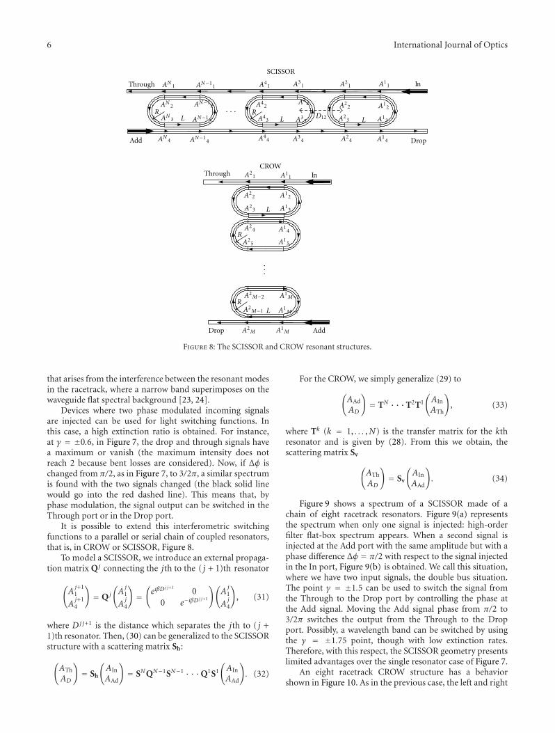
Figure 8: The SCISSOR and CROW resonant structures.
that arises from the interference between the resonant modesin the racetrack, where a narrow band superimposes on thewaveguide flat spectral background [23, 24].
Devices where two phase modulated incoming signalsare injected can be used for light switching functions. Inthis case, a high extinction ratio is obtained. For instance,at γ = ±0.6, in Figure 7, the drop and through signals havea maximum or vanish (the maximum intensity does notreach 2 because bent losses are considered). Now, if Δφ ischanged from π/2, as in Figure 7, to 3/2π, a similar spectrumis found with the two signals changed (the black solid linewould go into the red dashed line). This means that, byphase modulation, the signal output can be switched in theThrough port or in the Drop port.
It is possible to extend this interferometric switchingfunctions to a parallel or serial chain of coupled resonators,that is, in CROW or SCISSOR, Figure 8.
To model a SCISSOR, we introduce an external propaga-tion matrix Q j connecting the jth to the ( j + 1)th resonator
(A
j+11
Aj+14
)= Q j
(A
j1
Aj4
)=(eiβD
j j+10
0 e−iβDj j+1
)(A
j1
Aj4
), (31)
where Dj j+1 is the distance which separates the jth to ( j +1)th resonator. Then, (30) can be generalized to the SCISSORstructure with a scattering matrix Sh:
(ATh
AD
)= Sh
(AIn
AAd
)= SNQN−1SN−1 · · ·Q1S1
(AIn
AAd
). (32)
For the CROW, we simply generalize (29) to
(AAd
AD
)= TN · · ·T2T1
(AIn
ATh
), (33)
where Tk (k = 1, . . . ,N) is the transfer matrix for the kthresonator and is given by (28). From this we obtain, thescattering matrix Sv
(ATh
AD
)= Sv
(AIn
AAd
). (34)
Figure 9 shows a spectrum of a SCISSOR made of achain of eight racetrack resonators. Figure 9(a) representsthe spectrum when only one signal is injected: high-orderfilter flat-box spectrum appears. When a second signal isinjected at the Add port with the same amplitude but with aphase difference Δφ = π/2 with respect to the signal injectedin the In port, Figure 9(b) is obtained. We call this situation,where we have two input signals, the double bus situation.The point γ = ±1.5 can be used to switch the signal fromthe Through to the Drop port by controlling the phase atthe Add signal. Moving the Add signal phase from π/2 to3/2π switches the output from the Through to the Dropport. Possibly, a wavelength band can be switched by usingthe γ = ±1.75 point, though with low extinction rates.Therefore, with this respect, the SCISSOR geometry presentslimited advantages over the single resonator case of Figure 7.
An eight racetrack CROW structure has a behaviorshown in Figure 10. As in the previous case, the left and right
International Journal of Optics 7
2
1.5
1
0.5
0−3 −2 −1 0 1 2 3
γ (rad)
Nor
mal
ized
inte
nsi
ty
(a)
−3 −2 −1 0 1 2 3
γ (rad)
2
1.5
1
0.5
0
Nor
mal
ized
inte
nsi
ty
(b)
Figure 9: The single (a) and dual-bus (b) eight resonator SCISSOR spectrum for Δφ = π/2. (Drop: black solid line, Through: red dashedline).
−3 −2 −1 0 1 2 3
γ (rad)
2
1.5
1
0.5
0
Nor
mal
ized
inte
nsi
ty
(a)
2
1.5
1
0.5
0 −3 −2 −1 0 1 2 3
γ (rad)
Nor
mal
ized
inte
nsi
ty
(b)
Figure 10: The single (a) and dual-bus (b) eight resonator CROW spectrum for Δφ = π/2. (Lines as in Figure 9).
Add Drop
R
R
L
L
Th2
Th1 A21 A1
1
A12
A13A2
3
A24 A1
4
A25
A26 A1
6
A15
A17A2
7
A22
In1
In2
Figure 11: The resonator pair ds-coupler switch.
graphs represent the single- and double-bus spectra for thesame dephasing. CROW are very different from SCISSOR:given a N resonator CROW, the single bus device has N Dropresonances (Figure 10(a)) while the double bus device hasN − 1 bands when a Δφ = π/2 is considered (Figure 10(b)).
Also, in this case, for a dephasing of Δφ = (3/2)π, one canflip the Through ↔ Drop port outputs. Not all bands havethe same extinction efficiency, only the central ones exhibitan almost ideal on-off. The CROW has the advantage withrespect to the SCISSOR and single resonator that it allowsband routing or it can be used as an optical interleaver,that is, as a device that separates a set of channels into twosets, routing them separately towards the Drop and Throughports. The width of each band depends on the structuralparameters.
4. Three-Bus Resonator Interferometric Switch
A further interesting situation is to model a structure like thatof Figure 11. It shows a single pair of racetrack resonatorscoupled to three-bus waveguides. This interferometric switchworks as follows: the input signals In1 and In2 are tunedto a resonance wavelength and have the same amplitude.Then, depending on their relative phase, they interfereconstructively or destructively in the Drop waveguide. In theformer case, the signal is expected to couple into the Dropport, while, in the latter case, the signal is transmitted tothe Through ports. Experiments demonstrate this principle[11, 12].
8 International Journal of Optics
2
1.5
1
0.5
0
Nor
mal
ized
inte
nsi
ty
γ (rad)
−1.5 −1 −0.5 0 0.5 1 1.5
(a)
2
1.5
1
0.5
0
Nor
mal
ized
inte
nsi
ty
γ (rad)
−1.5 −1 −0.5 0 0.5 1 1.5
(b)
Figure 12: Spectral response of the device in Figure 11, with AIn1 = 1, AAd = 0, AIn2 = 0, L = 10μm (a), and L = 3μm (b) (Drop port: blacksolid line, Through1 port: red dashed line, Through2 port: blue dotted-dashed line).
In this section, we model the device as a three-bus device,that is, we drive it with three input signals whose phase isindependently controlled. To relate the known signals A1
1 =AIn1 , A2
4 = AAd, A17 = AIn2 to the unknown A2
1 = ATh1 ,A1
4 = AD, and A27 = ATh2 (Figure 11), we use a general
transfer matrix T:⎛⎜⎝ATh1
AD
ATh2
⎞⎟⎠ =
⎛⎜⎝T11 T21 T31
T21 T22 T21
T31 T21 T11
⎞⎟⎠⎛⎜⎝AIn1
AAd
AIn2
⎞⎟⎠ = T
⎛⎜⎝AIn1
AAd
AIn2
⎞⎟⎠, (35)
whose elements are reported in Appendix B. The device (andtherefore T) is symmetric: the paths In1 → Through1, In1 →Drop, In1 → Through2 are equivalent to the paths In2 →Through2, In2 → Drop, In2 → Through1.
Figure 12 shows the spectral response of the device whenused in single bus configuration, that is, only one input signalis injected (AIn1 = 1, AAd = 0, AIn2 = 0), for two couplingsection lengths of L = 10μm and L = 3μm. The drop signal(black line) shows a typical resonant behavior with a sharperfeature for the L = 3μm device than for the L = 10μm devicebecause of its lower coupling efficiency. It is also interestingto note that the crosstalk is much higher for L = 10μmthan for 3 μm. At resonance, the power is almost equallydistributed between the Drop and Through2 ports.
Figure 13 shows the case of a device operated in a dualsbus configuration. We used L = 10μm for the couplingsection. The input signals have the same amplitude and aphase difference of Δφ = 0,π/4, 3/4π,π for Figures 13(a),13(b), 13(c), 13(d), respectively. When the two input signalsare in phase, and the wavelength is resonant with the tworacetracks, then most of the power is transferred to theDrop port. This situation was experimentally confirmed in[11, 12].
The Through ports will not exhibit complete extinctiondue to crosstalk effects (Figure 13(a)). Similarly, when thetwo input signals are in antiphase (Figure 13(d)), a completedestructive interference is achieved in the Drop waveguideand no Drop signal is observed. Most of the power goesstraight in the Through ports. Note that the minima at reso-nance in the Through signals are due to the resonator round
trip losses. With no dephasing, the Through signal minimacoincide, with the Drop signal maximum at resonance λ0
(Figure 13(a)). In the other case, the Through signals showthe behaviors of a Fano resonance (Figures 13(b) and 13(c)).When there is a phase shift between the input signals, theThrough signals show characteristics of Fano resonance witha different minimum at λF = λ0 ± 0.8 nm. This occursalready for a small Δφ = π/10. Moreover, the Through signalresonance depth depends on the phase shift and vanishesalmost completely at Δφ = π/4 (Figure 13(b)). This ispotentially useful to build interferometric switching deviceswith good on-off extinctions.
To highlight the phase shift dependence, we repeated thecalculations at the resonant or at the Fano wavelengths (λ0
or λF , resp.) by varying Δφ. At the same time, we variedthe intensity of the input signals. The results are shown inFigure 14 for λ0 and in Figure 15 for λF , for |AIn2 |2 = δ ×|AIn1|2 with δ = (1, 0.75, 0.25, 0). Several features can beobserved. First, for perfect input balance (Figure 14(a) andFigure 15(a)), the Drop signal goes to zero at Δφ = π, whilethe Through signals vanish only for λF and not for λ0. For thisreason, interferometric switching is at λF than at λ0. Second,for λF (Figure 15), the three output signals (Drop, Through1
and Through2) vanish for three different values of Δφ: Δφ =π/4 the Through2, Δφ = π the Drop, and Δφ = 7/4π theThrough1. Third, the transmission of the input signals tothe through ports is more effective for λF than for λ0, whichmight be useful for practical purposes. Fourth, from Figures14 and 15, it is clear that an interferometric switch devicemust be robust against input signal imbalance.
Similar features are obtained for a device with L = 3μm.The main difference is that λF is more near to λ0 which makesdifficult the use of the Fano concepts for interferometricrouting.
A further extension of the ds-router concept is a doubleSCISSOR structure as shown in Figure 16. To model it, wetransform T (35) into the “scattering matrix” S such that⎛
⎜⎝ATh1
AAd
ATh2
⎞⎟⎠ = S
⎛⎜⎝AIn1
AD
AIn2
⎞⎟⎠. (36)
International Journal of Optics 9
2
1.5
1
0.5
0
Nor
mal
ized
inte
nsi
ty
γ (rad)
−1.5 −1 −0.5 0 0.5 1 1.5
(a)
2
1.5
1
0.5
0
Nor
mal
ized
inte
nsi
ty
γ (rad)
−1.5 −1 −0.5 0 0.5 1 1.5
λ0
λF
(b)
2
1.5
1
0.5
0
Nor
mal
ized
inte
nsi
ty
γ (rad)
−1.5 −1 −0.5 0 0.5 1 1.5
(c)
2
1.5
1
0.5
0
Nor
mal
ized
inte
nsi
ty
γ (rad)
−1.5 −1 −0.5 0 0.5 1 1.5
(d)
Figure 13: Spectral response of the device in Figure 11, with AIn1 = (1, ei(π/4), ei(3/4)π , eiπ) ((a), (b), (c), (d), resp.), AAd = 0, AIn2 = 1. (Linesas in Figure 12.)
After simple algebraic manipulation, one finds
S = 1T22
⎛⎜⎝T11T22 − T12T21 T12 T31T22 − T12T21
−T21 1 −T21
T31T22 − T12T21 T12 T11T22 − T12T21
⎞⎟⎠, (37)
where the lower indexes indicate the row × column elementof T.
Then, by introducing an external propagation matrix Qk
which connects the Through and Add ports of the kth pair ofresonators with the In and Drop ports of the (k+ 1)th pair as
⎛⎜⎝AInk+1
1
ADk+1
AInk+12
⎞⎟⎠ = Qk
⎛⎜⎝AThk
1
AAdk
AThk2
⎞⎟⎠ =
⎛⎜⎝eiβD
k0 0
0 e−iβDk0
0 0 eiβDk
⎞⎟⎠⎛⎜⎝ATh k
1
AAdk
AThk2
⎞⎟⎠
(k = 1, . . . ,N),(38)
we can express the general equations for the device ofFigure 16 with a total transfer matrix STot:
⎛⎜⎝AThN
1
AAdN
AThN2
⎞⎟⎠ = STot
⎛⎜⎝AIn1
1
AD1
AIn12
⎞⎟⎠ = SNQN−1SN−1 · · ·Q1S1
⎛⎜⎝AIn1
1
AD1
AIn12
⎞⎟⎠.(39)
And, finally, after inverting STot (37), we get⎛⎜⎝AThN
1
AD1
AThN2
⎞⎟⎠ = TTot
⎛⎜⎝AIn1
1
AAdN
AIn12
⎞⎟⎠, (40)
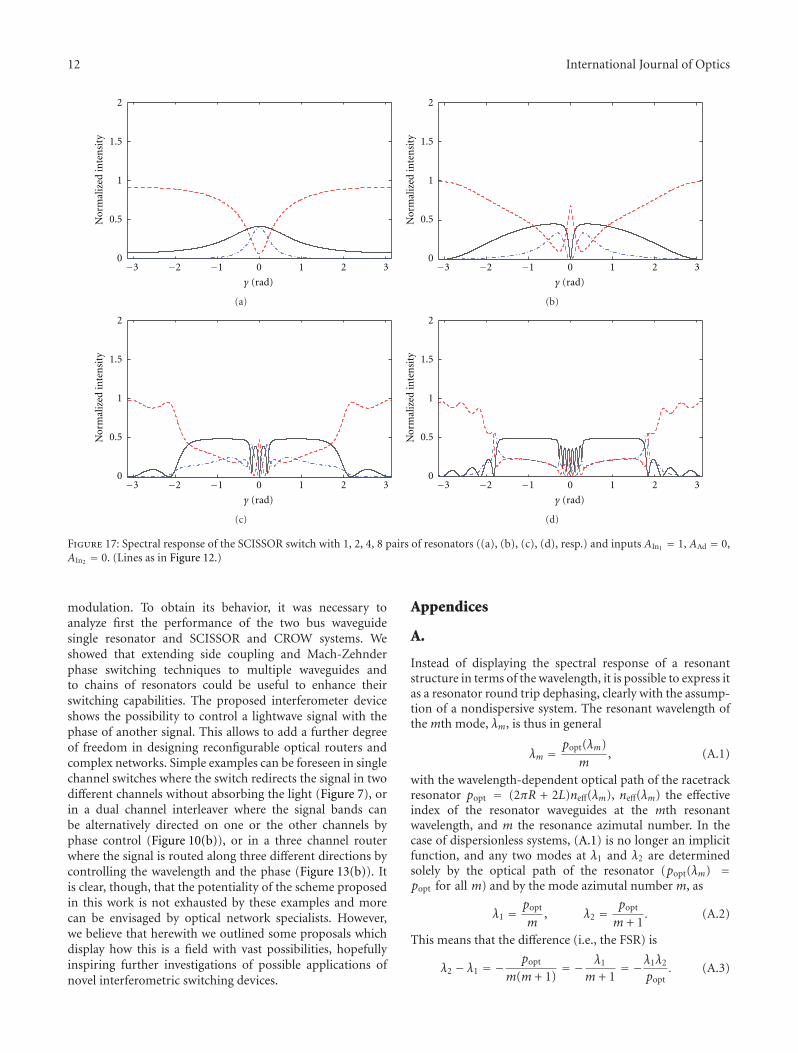
which is the generalized version of (35).Figure 17 shows the spectral response for the 1,2,4, and
8 pair SCISSOR interferometric switch (Figures 17(a), 17(b),17(c), 17(d), resp.) with only one input signal. The (N − 1)central dips are not due to fabrication imperfections [11, 12]but are intrinsic features due to the existence of the centralDrop waveguide between the two resonator chains. Thesystem behaves like a single SCISSOR row with asymmetricgaps which introduce a correspondent asymmetric phaseshift at each resonator gap leading to CRIT-like features. Itis in this spectral region, near the center of the resonanceband, where light couples more efficiently into the resonatorsand travels repeatedly through them producing slow lighteffects. For this reason, it is also in this central CRIT-like region where most of the attenuation occurs due toradiation and roughness losses on the resonator bent. Notehow, aside from the flat-box spectrum, despite strong inputimbalance, the two Through ports response (red dashedand blue dotted-dashed lines) tend to merge together insidethe mode’s spectral range with increasing the number of
10 International Journal of Optics
0 π/2 π 2π
Nor
mal
ized
inte
nsi
ty2
1.5
1
0.5
03π/2
Δφ (rad)
(a)
0 π/2 π 2π
Nor
mal
ized
inte
nsi
ty
2
1.5
1
0.5
03π/2
Δφ (rad)
(b)
0 π/2 π 2π
Nor
mal
ized
inte
nsi
ty
2
1.5
1
0.5
03π/2
Δφ (rad)
(c)
0 π/2 π 2π
Nor
mal
ized
inte
nsi
ty
2
1.5
1
0.5
03π/2
Δφ (rad)
(d)
Figure 14: Phase response of the device in Figure 11 at λ0, with AIn1 = eiΔΦ, AAd = 0, |AIn2 |2 = (1, 0.75, 0.25, 0) ((a), (b), (c), (d), resp.)(Lines as in Figure 12.)
resonator pairs. This is because in an N-pair SCISSOR theinput signals couple to the various resonator pairs, and,while they are propagating along the sequence, their poweris progressively balanced due to the large crosstalk. Thisrobustness of SCISSOR devices against input imbalancescould have practical advantages where a power injection isuncertain or difficult to tailor.
Figure 18 illustrates the use of a dual bus SCISSOR inter-ferometric switch with two equal input signals. Increasing thenumber of resonator, the response gets a flat-box shape anda good rejection of the input signal at the two Through portsis obtained.
Figure 19 shows the effect of a phase shift between thetwo input signals. As Δφ increases, the Drop signal decreasesand vanishes for Δφ = π. The Through signals are coincidentwithin the stop-band and differ outside this wavelengthregion when Δφ /= 0.
We studied also the effect of an imbalance betweenthe two input signals. A phase sweep at γ = 1 for fourdifferent intensities is shown in Figure 20. Contrary to thesingle pair interferometric switch affected by Fano resonanceasymmetries and unequal Through port signal intensitiesalong the phase sweep, the 2 × 8 SCISSOR interferometricswitch flattens out the differences on the Through signals andshows its robustness against imbalances.
Another potentially interesting application is to operate theds-coupler interferometric switch of Figure 11 with threeinput signals, that is, to use the Add port as a third inputport. Figure 21 shows its spectral response when AIn1 = eiφ1 ,AAd = eiφAdd , AIn2 = eiφ2 . Figure 21(a) shows the case of allthree equal input phases ((φ1, φAdd, φ2) = (0, 0, 0)): the Dropand the two Through signals are equal with slight differencescaused by the bending losses. Figure 21(b) reproduces thecase (φ1, φAdd, φ2) = (0,π/4,π/2): at the resonancewavelength, the two Through signals are high while the Dropsignals are low. The Through signal resonances are Fanoresonances. Figure 21(c) represents the alternative case whereonly a π-shift on the Add signal is applied ((φ1,φAdd,φ2) =(0,π, 0)): the Drop signal maximizes at resonance, while thetwo Through signals are low. Figure 21(d) shows the casewhen a π-shift is applied to both the Add and one Inputsignal (φ1,φAdd,φ2) = (0,π,π): all the input signals areaddressed to the Through1 port. The symmetric case wherethe signals are directed to the Through2 port is obtained byapplying the same phase shift to the other Input signal.
This three input signal configuration allows using theAdd signal as a control signal to drive the interferometric
International Journal of Optics 11
0 π/2 π 2π
Nor
mal
ized
inte
nsi
ty2
1.5
1
0.5
03π/2
Δφ (rad)
(a)
0 π/2 π 2π
Nor
mal
ized
inte
nsi
ty
2
1.5
1
0.5
03π/2
Δφ (rad)
(b)
0 π/2 π 2π
Nor
mal
ized
inte
nsi
ty
2
1.5
1
0.5
03π/2
Δφ (rad)
(c)
0 π/2 π 2π
Nor
mal
ized
inte
nsi
ty
2
1.5
1
0.5
03π/2
Δφ (rad)
(d)
Figure 15: Phase response of the device in Figure 11 at λF , with AIn1 = eiΔΦ, AAd = 0, |AIn2 |2 = (1, 0.75, 0.25, 0) ((a), (b), (c), (d), resp.).(Lines as in Figure 12.)
D1
D1
Add1Add2
Drop1
Drop1
· · ·
· · ·
ThN1 Th2
1 Th11
ThN2 Th2
2 Th12
InN1 In2
1 In11
InN2 In2
2 In12
AddN AddN−1
DropN−1
Figure 16: The 2×N SCISSOR phase switch.
switch to different functionalities (compare Figure 13 withFigure 21). In fact, if the phase of the Add signal is changedfrom 0 to π, the Drop signal is switched from 1 to 3 (inabsence of bending losses); while, if the phase of one ofthe input is changed from 0 to π and φAdd = π, one canswitch off and on the Through signals. Many other sortsof combinations in phase and intensity at the Input ports,resonator numbers, and overall resonant device geometry for
phase switching applications could be imagined in the mostdiverse configurations.
6. Conclusions
A three-bus waveguide multiple resonator-based interfer-ometric switching device was discussed which is able toroute light over a broad range of wavelengths by phase
12 International Journal of Optics
2
1.5
1
0.5
0−3 −2 −1 0 1 2 3
γ (rad)
Nor
mal
ized
inte
nsi
ty
(a)
2
1.5
1
0.5
0−3 −2 −1 0 1 2 3
γ (rad)
Nor
mal
ized
inte
nsi
ty
(b)
2
1.5
1
0.5
0−3 −2 −1 0 1 2 3
γ (rad)
Nor
mal
ized
inte
nsi
ty
(c)
2
1.5
1
0.5
0−3 −2 −1 0 1 2 3
γ (rad)
Nor
mal
ized
inte
nsi
ty
(d)
Figure 17: Spectral response of the SCISSOR switch with 1, 2, 4, 8 pairs of resonators ((a), (b), (c), (d), resp.) and inputs AIn1 = 1, AAd = 0,AIn2 = 0. (Lines as in Figure 12.)
modulation. To obtain its behavior, it was necessary toanalyze first the performance of the two bus waveguidesingle resonator and SCISSOR and CROW systems. Weshowed that extending side coupling and Mach-Zehnderphase switching techniques to multiple waveguides andto chains of resonators could be useful to enhance theirswitching capabilities. The proposed interferometer deviceshows the possibility to control a lightwave signal with thephase of another signal. This allows to add a further degreeof freedom in designing reconfigurable optical routers andcomplex networks. Simple examples can be foreseen in singlechannel switches where the switch redirects the signal in twodifferent channels without absorbing the light (Figure 7), orin a dual channel interleaver where the signal bands canbe alternatively directed on one or the other channels byphase control (Figure 10(b)), or in a three channel routerwhere the signal is routed along three different directions bycontrolling the wavelength and the phase (Figure 13(b)). Itis clear, though, that the potentiality of the scheme proposedin this work is not exhausted by these examples and morecan be envisaged by optical network specialists. However,we believe that herewith we outlined some proposals whichdisplay how this is a field with vast possibilities, hopefullyinspiring further investigations of possible applications ofnovel interferometric switching devices.
Appendices
A.
Instead of displaying the spectral response of a resonantstructure in terms of the wavelength, it is possible to express itas a resonator round trip dephasing, clearly with the assump-tion of a nondispersive system. The resonant wavelength ofthe mth mode, λm, is thus in general
λm =popt(λm)
m, (A.1)
with the wavelength-dependent optical path of the racetrackresonator popt = (2πR + 2L)neff(λm), neff(λm) the effectiveindex of the resonator waveguides at the mth resonantwavelength, and m the resonance azimutal number. In thecase of dispersionless systems, (A.1) is no longer an implicitfunction, and any two modes at λ1 and λ2 are determinedsolely by the optical path of the resonator (popt(λm) =popt for all m) and by the mode azimutal number m, as
λ1 =popt
m, λ2 =
popt
m + 1. (A.2)
This means that the difference (i.e., the FSR) is
λ2 − λ1 = −popt
m(m + 1)= − λ1
m + 1= −λ1λ2
popt. (A.3)
International Journal of Optics 13
2
1.5
1
0.5
0−3 −2 −1 0 1 2 3
γ (rad)
Nor
mal
ized
inte
nsi
ty
(a)
2
1.5
1
0.5
0−3 −2 −1 0 1 2 3
γ (rad)
Nor
mal
ized
inte
nsi
ty
(b)
2
1.5
1
0.5
0−3 −2 −1 0 1 2 3
γ (rad)
Nor
mal
ized
inte
nsi
ty
(c)
2
1.5
1
0.5
0−3 −2 −1 0 1 2 3
γ (rad)
Nor
mal
ized
inte
nsi
ty
(d)
Figure 18: Spectral response of the SCISSOR switch with 1, 2, 4, 8 pairs of resonators ((a), (b), (c), (d), resp.), and inputs AIn1 = 1, AAd = 0,AIn2 = 1, with same phase. (Lines as in Figure 12.)
Then, the parameter γ representing the round-trip de-phasing of the resonator can be defined as an “angulardeviation” from resonance at some wavelength λ as
λ = λ1 +γ
2π(λ2 − λ1) = λ1 − γ
2πλ1λ2
popt, (A.4)
and from which
γ = 2πpoptλ1 − λ
λ1λ2≈ 2πpopt
Δλ
λ2. (A.5)
B.
In Figure 11, we can relate (A23,A2
4,A25) → (A1
3,A14,A1
5)through (13) as
⎛⎜⎝A1
3
A14
A15
⎞⎟⎠ =M
⎛⎜⎝A2
3
A24
A25
⎞⎟⎠ =
⎛⎜⎝
t′ iκD −κ′iκD tD iκD−κ′ iκD t′
⎞⎟⎠⎛⎜⎝A2
3
A24
A25
⎞⎟⎠. (B.1)
Proceeding in the same way as we have done with matrixM of (25), we look for the coupling matrix that relates inthe interference section the upper to the lower waveguide
through the middle one, that is, (A23,A2
4,A13) → (A2
5,A14,A1
5),and obtain the second transfer matrix Tb:⎛⎜⎝A2
5
A14
A15
⎞⎟⎠ = Tb
⎛⎜⎝A2
3
A24
A13
⎞⎟⎠
= 1κ′
⎛⎜⎝
t′ iκD −1iκD(κ′ + t′) tDκ′ − κ2
D −iκDt′2 − κ′2 iκD(κ′ + t′) −t′
⎞⎟⎠⎛⎜⎝A2
3
A24
A13
⎞⎟⎠.
(B.2)
Due to a symmetric coupling, K of (26) can be appliedalso at (A1
6,A26) → (A1
7,A27). For the same reason, the same
internal propagation matrix of (27) can be applied also at(A2
5,A15) → (A1
6,A26). Therefore, the third transfer matrix
connects (A25,A1
5) → (A17,A2
7) in the same way as (28) (butwith the order of the propagation and coupling matrixesinverted):
(A1
7
A27
)= TKP
(A2
5
A15
)= KP
(A2
5
A15
). (B.3)
To proceed in the inverse direction, that is, from ports(In2, Through2) to (In1, Through1), note that, again becauseof coupling symmetry, TPK relates also (A1
7,A27) → (A2
5,A15),
TKP does the same with (A23,A1
3) → (A11,A2
1), and Tb con-nects also (A2
5,A24,A1
5) → (A23,A1
4,A13).
14 International Journal of Optics
2
1.5
1
0.5
0−3 −2 −1 0 1 2 3
γ (rad)
Nor
mal
ized
inte
nsi
ty
(a)
2
1.5
1
0.5
0−3 −2 −1 0 1 2 3
γ (rad)
Nor
mal
ized
inte
nsi
ty
(b)
2
1.5
1
0.5
0−3 −2 −1 0 1 2 3
γ (rad)
Nor
mal
ized
inte
nsi
ty
(c)
2
1.5
1
0.5
0−3 −2 −1 0 1 2 3
γ (rad)
Nor
mal
ized
inte
nsi
ty
(d)
Figure 19: Spectral response of the 2 × 8 SCISSOR switch of Figure 16 with inputs, AIn1 = (1, ei(π/2), ei(3/4)π , eiπ) ((a), (b), (c), (d) resp.),AAd = 0, AIn2 = 1 (Lines as in Figure 12.)
Now, we can obtain the overall device response ofFigure 11 by separating the contributions to the two Throughand the Drop ports as the sum of three different terms corre-sponding to the three following device states.
State (I). Input signal in In1 only is injected and propagatedfrom the top to the bottom of the device
⎛⎜⎝AIn1 =
∣∣AIn1
∣∣eiφ1
AAd = 0AIn2 = 0
⎞⎟⎠ �−→
⎛⎜⎝ATh(I)
1
AD(I)
ATh(I)2
⎞⎟⎠. (B.4)
Schematically, this goes as follows (from the right to theleft):
←−(A2
3
A13
)= TPK
(AIn1
ATh(I)1
)(B.5)
←−⎛⎜⎝
A25
AD(I)
A15
⎞⎟⎠ = Tb
⎛⎜⎝A2
3
0A1
3
⎞⎟⎠←− (B.6)
(0
ATh(I)2
)= TKP
(A2
5
A15
)←− . (B.7)
This means that the first set of equations from the firsttransferral of (B.5)
A23 = TPK
11 AIn1 + TPK12 ATh(I)
1,
A13 = TPK
21 AIn1 + TPK22 ATh(I)
1,
(B.8)
have to be inserted into (B.6) to obtain
A25 =
(Tb
11TPK11 + Tb
13TPK21
)AIn1
+(Tb
11TPK12 + Tb
13TPK22
)ATh(I)
1,
(B.9)
AD(I) =(Tb
21TPK11 + Tb
23TPK21
)AIn1
+(Tb
21TPK12 + Tb
23TPK22
)ATh(I)
1,
(B.10)
A15 =
(Tb
31TPK11 + Tb
33TPK21
)AIn1
+(Tb
31TPK12 + Tb
33TPK22
)ATh(I)
1.
(B.11)
Proceeding further with the next transfer, we have from(B.7) that
0 = TKP11 A
25 + TKP
12 A15,
ATh (I)2= TKP
21 A25 + TKP
22 A15,
(B.12)
International Journal of Optics 15
0 π/2 π 2π
Nor
mal
ized
inte
nsi
ty2
1.5
1
0.5
03π/2
Δφ (rad)
(a)
0 π/2 π 2π
Nor
mal
ized
inte
nsi
ty
2
1.5
1
0.5
03π/2
Δφ (rad)
(b)
0 π/2 π 2π
Nor
mal
ized
inte
nsi
ty
2
1.5
1
0.5
03π/2
Δφ (rad)
(c)
0 π/2 π 2π
Nor
mal
ized
inte
nsi
ty
2
1.5
1
0.5
03π/2
Δφ (rad)
(d)
Figure 20: Phase response of the 2 × 8 SCISSOR switch of Figure 16 with input imbalances |AIn1 |2 = (1, 0.25, 0.1, 0) ((a), (b), (c), (d),resp.), AAd = 0, AIn2 = 1, at phase round-trip shift γ = 1 (Lines as in Figure 12.)
which, through (B.9), (B.10), and (B.11), leads to
ATh(I)1= T11AIn1 ,
AD(I) = T21AIn1 ,
ATh(I)2= T31AIn1 ,
(B.13)
with
T11 = − TKP11 A + TKP
12 B
TKP11 C + TKP
12 D,
T21 = E + FT11,
T31 = G + HT11,
A = Tb11T
PK11 + Tb
13TPK21 ,
B = Tb31T
PK11 + Tb
33TPK21 ,
C = Tb11T
PK12 + Tb
13TPK22 ,
D = Tb31T
PK12 + Tb
33TPK22 ,
E = Tb21T
PK11 + Tb
23TPK21 ,
F = Tb21T
PK12 + Tb
23TPK22 ,
G = TKP21 A + TKP
22 B,
H = TKP21 C + TKP
22 D.
(B.14)
State (II). Input signal in In2 only is injected and propagatedfrom the bottom to the top of the device.
⎛⎜⎝
AIn1 = 0AAd = 0
AIn2 =∣∣AIn2
∣∣eiφ2
⎞⎟⎠ �−→
⎛⎜⎝ATh(III)
1
AD(III)
ATh(III)2
⎞⎟⎠. (B.15)
One proceeds exactly as for State (I), but in the oppositedirection. The only difference in the final result is that in
(B.13) the ports (In1, Through(I)1 , Through(I)
2 ) have to be
exchanged with (In2, Through(III)2 , Through(III)
1 ):
ATh(III)1= T13AIn2 ,
ADrop(III) = T23AIn2 ,
ATh(III)2= T33AIn2 ,
(B.16)
with T13 = T31, T23 = T21, and T33 = T11.
State (III). Add port signal only is injected and propagatedfrom the central Add waveguide towards the Drop and upperand lower Through ports.
In the transfer matrix of (35), only one coefficient ismissing, namely, T22. This is fixed by the other matrix ele-ments and power conservation criteria. Expressing explicitly
with the matrix elements of T the power balance between theinput and output intensities of the waves, it must hold:
∣∣AIn1
∣∣2 +∣∣AIn2
∣∣2 + |AAd|2
= ∣∣ATh1
∣∣2 + |AD|2 +∣∣ATh2
∣∣2 + Loss
=(|T11|2 + |T21|2 + |T31|2
)(∣∣AIn1
∣∣2 +∣∣AIn2
∣∣2)
+(
2|T21|2 + |T22|2)|AAd|2
+(T11T
∗31 + |T21|2 + T31T
∗11
)(AIn1A
∗In2
+ A∗In1AIn2
)
+(T11T
∗21 + T21T
∗22 + T31T
∗21
)(AIn1 + AIn1
)A∗Ad
+(T∗11T21 + T∗21T22 + T∗31T21
)(A∗In1
+ AIn2
)AAd + Loss,
(B.17)
with the last term indicating the losses of the structure. Thisimplies the following conditions:
|T11|2 + |T21|2 + |T31|2 = 1, (B.18)
2|T21|2 + |T22|2 = 1, (B.19)
T11T∗31 + |T21|2 + T31T
∗11 = 0, (B.20)
T∗11T21 + T∗21T22 + T∗31T21 = 0. (B.21)
Conditions (B.18) and (B.20) are already satisfied bythe coefficients found in the two previous cases (verycumbersome and long calculations). From (B.21), we finallyobtain the last coefficient for matrix (35):
T22 = −T21
T∗21
(T∗11 + T∗31
), (B.22)
which satisfies also (B.19) through (B.20).
Acknowledgment
The authors acknowledge support of the EU through theFP7 ICT-(216405) Project Wavelength Division MultiplexedPhotonic Layer on CMOS.
References
[1] T. S. El-Bawab, Optical Switching, Springer, 2006.
International Journal of Optics 17
[2] A. Yariv, Y. Xu, R. K. Lee, and A. Scherer, “Coupled-resonatoroptical waveguide: a proposal and analysis,” Optics Letters, vol.24, no. 11, pp. 711–713, 1999.
[3] J. E. Heebner, R. W. Boyd, and Q. H. Park, “SCISSOR soli-tons and other novel propagation effects in microresonator-modified waveguides,” Journal of the Optical Society of AmericaB, vol. 19, no. 4, pp. 722–731, 2002.
[4] J. E. Heebner, P. Chak, S. Pereira, J. E. Sipe, and R. W. Boyd,“Distributed and localized feedback in microresonatorsequences for linear and nonlinear optics,” Journal of the Opti-cal Society of America B, vol. 21, no. 10, pp. 1818–1832, 2004.
[5] J. Capmany, P. Munoz, J. D. Domenech, and M. A. Muriel,“Apodized coupled resonator waveguides,” Optics Express, vol.15, no. 16, pp. 10196–10206, 2007.
[6] S. Y. Cho and R. Soref, “Apodized SCISSORs for filtering andswitching,” Optics Express, vol. 16, no. 23, pp. 19078–19090,2008.
[7] D. U. Smith, H. Chang, K. A. Fuller, A. T. Rosenberger, and R.W. Boyd, “Coupled-resonator-induced transparency,” PhysicalReview A, vol. 69, no. 6, Article ID 063804, 6 pages, 2004.
[8] Q. Xu, S. Sandhu, M. L. Povinelli, J. Shakya, S. Fan, and M.Lipson, “Experimental realization of an on-chip all-opticalanalogue to electromagnetically induced transparency,” Phys-ical Review Letters, vol. 96, no. 12, Article ID 123901, 4 pages,2006.
[9] Y. F. Xiao, X. B. Zou, W. Jiang, Y. L. Chen, and G. C. Guo,“Analog to multiple electromagnetically induced transparencyin all-optical drop-filter systems,” Physical Review A, vol. 75,no. 6, Article ID 063833, 4 pages, 2007.
[10] X. Yang, M. Yu, D. L. Kwong, and C. W. Wong, “All-opticalanalog to electromagnetically induced transparency in multi-ple coupled photonic crystal cavities,” Physical Review Letters,vol. 102, no. 17, Article ID 173902, 4 pages, 2009.
[11] M. Mancinelli, R. Guider, M. Masi et al., “Optical character-ization of a SCISSOR device,” Optics Express, vol. 19, no. 14,pp. 13664–13674, 2011.
[12] M. Masi, M. Mancinelli, A. Battarelli et al., “A silicon photonicinterferometric router device based on SCISSOR concept,”Journal of Lightwave Technology, vol. 29, no. 18, pp. 2747–2753,2011.
[14] G. T. Reed, G. Mashanovich, F. Y. Gardes, and D. J. Thomson,“Silicon optical modulators,” Nature Photonics, vol. 4, article660, 2010.
[15] K. Okamoto, Fundamentals of Optical Waveguides, AcademicPress, 2nd edition, 2006.
[16] Y. M. Landobasa, S. Darmawan, and M. K. Chin, “Matrix anal-ysis of 2-d microresonator lattice optical filters,” IEEE Journalof Quantum Electronics, vol. 41, no. 11, pp. 1410–1418, 2005.
[17] J. K. S. Poon, J. Scheuer, S. Mookherjea, G. T. Paloczi, Y.Huang, and A. Yariv, “Matrix analysis of microring coupled-resonator optical waveguides,” Optics Express, vol. 12, no. 1,pp. 90–103, 2004.
[18] C.-S. Ma, X. Yan, and X.-Y. Wang, “Matrix analysis of 2Dmicroring resonator arrays,” Journal of Modern Optics, vol. 55,no. 1, pp. 143–154, 2008.
[19] J. K. S. Poon, P. Chak, J. M. Choi, and A. Yariv, “Slowing lightwith Fabry-Perot resonator arrays,” Journal of the Optical Soci-ety of America B, vol. 24, no. 11, pp. 2763–2769, 2007.
[20] S. Y. Cho and R. Soref, “Interferometric microring-resonant2×2 optical switches,” Optics Express, vol. 16, no. 17, pp.13304–13314, 2008.
[21] F. Xia, L. Sekaric, M. O’Boyle, and Y. Vlasov, “Coupled res-onator optical waveguides based on silicon-on-insulator pho-tonic wires,” Applied Physics Letters, vol. 89, no. 4, Article ID041122, 3 pages, 2006.
[22] M. Masi, R. Orobtchouk, G. Fan, J. M. Fedeli, and L. Pavesi,“Towards a realistic modelling of ultra-compact racetrackresonators,” Journal of Lightwave Technology, vol. 28, no. 22,pp. 3233–3242, 2010.
[23] U. Fano, “Sullo spettro di assorbimento dei gas nobili presso illimite dello spettro d’arco,” Nuovo Cimento, vol. 12, no. 3, pp.154–161, 1935.
[24] U. Fano, “Effects of configuration interaction on intensitiesand phase shifts,” Physical Review, vol. 124, no. 6, pp. 1866–1878, 1961.