Resistive Computation: Avoiding the Power Wall with Low-Leakage, STT-MRAM Based Computing Xiaochen Guo Engin ˙ Ipek Tolga Soyata University of Rochester Rochester, NY 14627 USA {xiguo, ipek, soyata}@ece.rochester.edu ABSTRACT As CMOS scales beyond the 45nm technology node, leakage concerns are starting to limit microprocessor performance growth. To keep dynamic power constant across process gen- erations, traditional MOSFET scaling theory prescribes re- ducing supply and threshold voltages in proportion to device dimensions, a practice that induces an exponential increase in subthreshold leakage. As a result, leakage power has be- come comparable to dynamic power in current-generation processes, and will soon exceed it in magnitude if voltages are scaled down any further. Beyond this inflection point, multicore processors will not be able to afford keeping more than a small fraction of all cores active at any given moment. Multicore scaling will soon hit a power wall. This paper presents resistive computation, a new tech- nique that aims at avoiding the power wall by migrating most of the functionality of a modern microprocessor from CMOS to spin-torque transfer magnetoresistive RAM (STT- MRAM)—a CMOS-compatible, leakage-resistant, non-volatile resistive memory technology. By implementing much of the on-chip storage and combinational logic using leakage- resistant, scalable RAM blocks and lookup tables, and by carefully re-architecting the pipeline, an STT-MRAM based implementation of an eight-core Sun Niagara-like CMT pro- cessor reduces chip-wide power dissipation by 1.7× and leak- age power by 2.1× at the 32nm technology node, while main- taining 93% of the system throughput of a CMOS-based de- sign. Categories and Subject Descriptors B.3.1 [Memory Structures]: Semiconductor Memories; C.1.4 [Processor Architectures]: Parallel Architectures General Terms Design, Performance Keywords Power-efficiency, STT-MRAM Permission to make digital or hard copies of all or part of this work for personal or classroom use is granted without fee provided that copies are not made or distributed for profit or commercial advantage and that copies bear this notice and the full citation on the first page. To copy otherwise, to republish, to post on servers or to redistribute to lists, requires prior specific permission and/or a fee. ISCA’10, June 19–23, 2010, Saint-Malo, France. Copyright 2010 ACM 978-1-4503-0053-7/10/06 ...$10.00. 1. INTRODUCTION Over the past two decades, the CMOS microprocessor de- sign process has been confronted by a number of seemingly insurmountable technological challenges (e.g., the memory wall [4] and the wire delay problem [1]). At each turn, new classes of systems have been architected to meet these challenges, and microprocessor performance has continued to scale with exponentially increasing transistor budgets. With more than two billion transistors integrated on a sin- gle die [27], power dissipation has become the current crit- ical challenge facing modern chip design. On-chip power dissipation now exhausts the maximum capability of con- ventional cooling technologies; any further increases will re- quire expensive and challenging solutions (e.g., liquid cool- ing), which would significantly increase overall system cost. Multicore architectures emerged in the early 2000s as a means of avoiding the power wall, increasing parallelism un- der a constant clock frequency to avoid an increase in dy- namic power consumption. Although multicore systems did manage to keep power dissipation at bay for the past decade, with the impending transition to 32nm CMOS, they are starting to experience scalability problems of their own. To maintain constant dynamic power at a given clock rate, sup- ply and threshold voltages must scale with feature size, but this approach induces an exponential rise in leakage power, which is fast approaching dynamic power in magnitude. Un- der this poor scaling behavior, the number of active cores on a chip will have to grow much more slowly than the total transistor budget allows; indeed, at 11nm, over 80% of all cores may have to be dormant at all times to fit within the chip’s thermal envelope [16]. This paper presents resistive computation, an architec- tural technique that aims at developing a new class of power- efficient, scalable microprocessors based on emerging resis- tive memory technologies. Power- and performance-critical hardware resources such as caches, memory controllers, and floating-point units are implemented using spin-torque trans- fer magnetoresistive RAM (STT-MRAM)—a CMOS- com- patible, near-zero static-power, persistent memory that has been in development since the early 2000s [12], and is ex- pected to replace commercially available magnetic RAMs by 2013 [13]. The key idea is to implement most of the on- chip storage and combinational logic using scalable, leakage- resistant RAM arrays and lookup tables (LUTs) constructed from STT-MRAM to lower leakage, thereby allowing many more active cores under a fixed power budget than a pure CMOS implementation could afford. By adopting hardware structures amenable to fast and ef- ficient LUT-based computing, and by carefully re-architecting the pipeline, an STT-MRAM based implementation of an eight-core, Sun Niagara-like CMT processor reduces leakage and total power at 32nm by 2.1× and 1.7×, respectively, while maintaining 93% of the system throughput of a pure CMOS implementation. 371
Transcript
Resistive Computation: Avoiding the Power Wall withLow-Leakage, STT-MRAM Based Computing
ABSTRACTAs CMOS scales beyond the 45nm technology node, leakageconcerns are starting to limit microprocessor performancegrowth. To keep dynamic power constant across process gen-erations, traditional MOSFET scaling theory prescribes re-ducing supply and threshold voltages in proportion to devicedimensions, a practice that induces an exponential increasein subthreshold leakage. As a result, leakage power has be-come comparable to dynamic power in current-generationprocesses, and will soon exceed it in magnitude if voltagesare scaled down any further. Beyond this inflection point,multicore processors will not be able to afford keeping morethan a small fraction of all cores active at any given moment.Multicore scaling will soon hit a power wall.
This paper presents resistive computation, a new tech-nique that aims at avoiding the power wall by migratingmost of the functionality of a modern microprocessor fromCMOS to spin-torque transfer magnetoresistive RAM (STT-MRAM)—a CMOS-compatible, leakage-resistant, non-volatileresistive memory technology. By implementing much ofthe on-chip storage and combinational logic using leakage-resistant, scalable RAM blocks and lookup tables, and bycarefully re-architecting the pipeline, an STT-MRAM basedimplementation of an eight-core Sun Niagara-like CMT pro-cessor reduces chip-wide power dissipation by 1.7× and leak-age power by 2.1× at the 32nm technology node, while main-taining 93% of the system throughput of a CMOS-based de-sign.
Permission to make digital or hard copies of all or part of this work forpersonal or classroom use is granted without fee provided that copies arenot made or distributed for profit or commercial advantage and that copiesbear this notice and the full citation on the first page. To copy otherwise, torepublish, to post on servers or to redistribute to lists, requires prior specificpermission and/or a fee.ISCA’10, June 19–23, 2010, Saint-Malo, France.Copyright 2010 ACM 978-1-4503-0053-7/10/06 ...$10.00.
1. INTRODUCTIONOver the past two decades, the CMOS microprocessor de-
sign process has been confronted by a number of seeminglyinsurmountable technological challenges (e.g., the memorywall [4] and the wire delay problem [1]). At each turn,new classes of systems have been architected to meet thesechallenges, and microprocessor performance has continuedto scale with exponentially increasing transistor budgets.With more than two billion transistors integrated on a sin-gle die [27], power dissipation has become the current crit-ical challenge facing modern chip design. On-chip powerdissipation now exhausts the maximum capability of con-ventional cooling technologies; any further increases will re-quire expensive and challenging solutions (e.g., liquid cool-ing), which would significantly increase overall system cost.
Multicore architectures emerged in the early 2000s as ameans of avoiding the power wall, increasing parallelism un-der a constant clock frequency to avoid an increase in dy-namic power consumption. Although multicore systems didmanage to keep power dissipation at bay for the past decade,with the impending transition to 32nm CMOS, they arestarting to experience scalability problems of their own. Tomaintain constant dynamic power at a given clock rate, sup-ply and threshold voltages must scale with feature size, butthis approach induces an exponential rise in leakage power,which is fast approaching dynamic power in magnitude. Un-der this poor scaling behavior, the number of active coreson a chip will have to grow much more slowly than the totaltransistor budget allows; indeed, at 11nm, over 80% of allcores may have to be dormant at all times to fit within thechip’s thermal envelope [16].
This paper presents resistive computation, an architec-tural technique that aims at developing a new class of power-efficient, scalable microprocessors based on emerging resis-tive memory technologies. Power- and performance-criticalhardware resources such as caches, memory controllers, andfloating-point units are implemented using spin-torque trans-fer magnetoresistive RAM (STT-MRAM)—a CMOS- com-patible, near-zero static-power, persistent memory that hasbeen in development since the early 2000s [12], and is ex-pected to replace commercially available magnetic RAMsby 2013 [13]. The key idea is to implement most of the on-chip storage and combinational logic using scalable, leakage-resistant RAM arrays and lookup tables (LUTs) constructedfrom STT-MRAM to lower leakage, thereby allowing manymore active cores under a fixed power budget than a pureCMOS implementation could afford.
By adopting hardware structures amenable to fast and ef-ficient LUT-based computing, and by carefully re-architectingthe pipeline, an STT-MRAM based implementation of aneight-core, Sun Niagara-like CMT processor reduces leakageand total power at 32nm by 2.1× and 1.7×, respectively,while maintaining 93% of the system throughput of a pureCMOS implementation.
371
2. BACKGROUND AND MOTIVATIONSimultaneously to power-related problems in CMOS, DRAM
is facing severe scalability problems due to precise chargeplacement and sensing hurdles in deep-submicron processes.In response, the industry is turning its attention to resistivememory technologies such as phase-change memory (PCM),memristors (RRAM), and spin-torque transfer magnetore-sistive RAM (STT-MRAM)—memory technologies that relyon resistivity rather than charge as the information carrier,and thus hold the potential to scale to much smaller geome-tries than charge memories [13]. Unlike the case of SRAMor DRAM, resistive memories rely on non-volatile, resistiveinformation storage in a cell, and thus exhibit near-zero leak-age in the data array.
2.1 STT-MRAMSTT-MRAM [13,20,31–33] is a second generation MRAM
technology that addresses many of the scaling problems ofcommercially available toggle-mode magnetic RAMs. Amongall resistive memories, STT-MRAM is the closest to beinga CMOS-compatible universal memory technology as it of-fers read speeds as fast as SRAM [39] (< 200ps in 90nm),density comparable to DRAM (10F 2), scalable energy char-acteristics [13], and infinite write endurance. Functionalarray prototypes [14, 20, 31], CAM circuits [37], and simu-lated FPGA chips [39] using STT-MRAM have already beendemonstrated, and the technology is under rapid commercialdevelopment, with an expected industry-wide switch fromtoggle-mode MRAM to STT-MRAM by 2013 [13]. AlthoughMRAM suffers from relatively high write power and writelatency compared to SRAM, its near-zero leakage power dis-sipation, coupled with its fast read speed and scalabilitymakes it a promising candidate to take over as the workhorsefor on-chip storage in sub-45nm processes.
Memory Cells and Array Architecture. STT-MRAMrelies on magnetoresistance to encode information. Figure 1depicts the fundamental building block of an MRAM cell,the magnetic tunnel junction (MTJ). An MTJ consists oftwo ferromagnetic layers and a tunnel barrier layer, oftenimplemented using a magnetic thin-film stack comprisingCo40Fe40B20 for the ferromagnetic layers, and MgO for thetunnel barrier. One of the ferromagnetic layers, the pinnedlayer, has a fixed magnetic spin, whereas the spin of theelectrons in the free layer can be influenced by first applyinga high-amplitude current pulse through the pinned layer topolarize the current, and then passing this spin-polarizedcurrent through the free layer. Depending on the directionof the current, the spin polarity of the free layer can be madeeither parallel or anti-parallel to that of the pinned layer.
MgO
Pinned Layer
RP
(a) (b)
Free Layer
MgO
Pinned Layer
RAPFree Layer
Figure 1: Illustrative example of a magneto-tunnel junction(MTJ) in (a) low-resistance parallel and (b) high-resistanceanti-parallel states.
Applying a small bias voltage (typically 0.1V) across theMTJ causes a tunneling current to flow through the MgOtunnel barrier without perturbing the magnetic polarity ofthe free layer. The magnitude of the tunneling current—andthus, the resistance of the MTJ—is determined by the po-larity of the two ferromagnetic layers: a lower, parallel resis-tance (RP in Figure 1-a) state is experienced when the spinpolarities agree, and a higher, antiparallel resistance stateis observed when the polarities disagree (RAP in Figure 1-b). When the polarities of the two layers are aligned, elec-
trons with polarity anti-parallel to the two layers can travelthrough the MTJ easily, while electrons with the same spinas the two layers are scattered; in contrast, when the twolayers have anti-parallel polarities, electrons of either polar-ity are largely scattered by one of the two layers, leadingto much lower conductivity, and thus, higher resistance [6].These low and high resistances are used to represent differ-ent logic values.
The most commonly used structure for an STT-MRAMmemory cell is the 1T-1MTJ cell that comprises a singleMTJ, and a single transistor that acts as an access device(Figure 2). Transistors are built in CMOS, and the MTJmagnetic material is grown over the source and drain re-gions of the transistors through a few (typically two or three)additional process steps. Similarly to SRAM and DRAM,1T-1MTJ cells can be coupled through wordlines and bit-lines to form memory arrays. Each cell is read by drivingthe appropriate wordline to connect the relevant MTJ toits bitline (BL) and source line (SL), applying a small biasvoltage (typically 0.1V ) across the two, and by sensing thecurrent passing through the MTJ using a current sense am-plifier connected to the bitline. Read speed is determinedby how fast the capacitive wordline can be charged to turnon the access transistor, and by how fast the bitline can beraised to the required read voltage to sample the read-outcurrent. The write operation, on the other hand, requiresactivating the access transistor, and applying a much highervoltage (typically Vdd) that can generate enough current tomodify the spin of the free layer.
WL
BLSL
Figure 2: Illustrative example of a 1T-1MTJ cell.
An MTJ can be written in a thermal activation modethrough the application of a long, low-amplitude currentpulse (>10ns), under a dynamic reversal regime with inter-mediate current pulses (3-10ns), or in a precessional switch-ing regime with a short (<3ns), high-amplitude current pulse [12].In a 1T-1MTJ cell with a fixed-size MTJ, a tradeoff existsbetween switching time (i.e., current pulse width) and cellarea. In precessional mode, the required current densityJc(τ) to switch the state of the MTJ is inversely propor-tional to switching time τ
Jc(τ) ∝ Jc0 +C
τwhere Jc0 is a process-dependent intrinsic current densityparameter, and C is a constant that depends on the angle ofthe magnetization vector of the free layer [12]. Hence, oper-ating at a faster switching time increases energy-efficiency:a 2× shorter write pulse requires a less than 2× increasein write current, and thus, lower write energy [8, 20, 26].Unfortunately, the highest switching speed possible with afixed-size MTJ is restricted by two fundamental factors: (1)the maximum current that the cell can can support duringan RAP → RP transition cannot exceed RAP /V dd since thecell has to deliver the necessary switching current over theMTJ in its high-resistance state, and (2) a higher switchingcurrent requires the access transistor to be sized larger sothat it can source the required current, which increases cellarea 1 and hurts read energy and delay due to higher gatecapacitance.
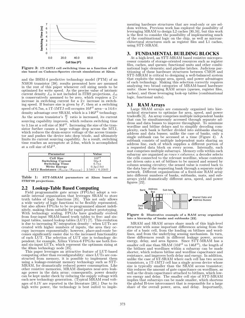
Figure 3 shows 1T-1MTJ cell switching time as a func-tion of cell area based on Cadence-Spectre analog circuitsimulations of a single cell at the 32nm technology node,using ITRS 2009 projections on MTJ parameters (Table 1),
1The MTJ is grown above the source and drain regions ofthe access transistor and is typically much smaller than thetransistor itself; consequently, the size of the access transis-tor determines cell area.
372
0 1 2 3 4 5 6 7
0.0 20.0 40.0 60.0
Switching Time (ns)
Cell Size (F2)
Figure 3: 1T-1MTJ cell switching time as a function of cellsize based on Cadence-Spectre circuit simulations at 32nm.
and the BSIM-4 predictive technology model (PTM) of anNMOS transistor [38]; results presented here are assumedin the rest of this paper whenever cell sizing needs to beoptimized for write speed. As the precise value of intrinsiccurrent density Jc0 is not included in ITRS projections, Jc0
is conservatively assumed to be zero, which requires a 2×increase in switching current for a 2× increase in switch-ing speed. If feature size is given by F , then at a switchingspeed of 6.7ns, a 1T-1MTJ cell occupies 10F 2 area—a 14.6×density advantage over SRAM, which is a 146F 2 technology.As the access transistor’s W
Lratio is increased, its current
sourcing capability improves, which reduces switching timeto 3.1ns at a cell size of 30F 2. Increasing the size of the tran-sistor further causes a large voltage drop across the MTJ,which reduces the drain-source voltage of the access transis-tor and pushes the device into deep triode, and ultimatelylimits its current sourcing capability. As a result, switchingtime reaches an asymptote at 2.6ns, which is accomplishedat a cell size of 65F 2.
Parameter Value
Cell Size 10F 2
Switching Current 50µASwitching Time 6.7nsWrite Energy 0.3pJ/bit
MTJ Resistance (RLOW /RHIGH) 2.5kΩ / 6.25kΩ
Table 1: STT-MRAM parameters at 32nm based onITRS’09 projections.
2.2 Lookup-Table Based ComputingField programmable gate arrays (FPGAs) adopt a ver-
satile internal organization that leverages SRAM to storetruth tables of logic functions [35]. This not only allowsa wide variety of logic functions to be flexibly represented,but also allows FPGAs to be re-programmed almost indefi-nitely, making them suitable for rapid product prototyping.With technology scaling, FPGAs have gradually evolvedfrom four-input SRAM-based truth tables to five- and six-input tables, named lookup tables (LUT) [7]. This evolutionis due to increasing IC integration density—when LUTs arecreated with higher numbers of inputs, the area they oc-cupy increases exponentially; however, place-and-route be-comes significantly easier due to the increased functionalityof each LUT. The selection of LUT size is technology de-pendent; for example, Xilinx Virtex-6 FPGAs use both five-and six-input LUTs, which represent the optimum sizing atthe 40nm technology node [35].
This paper leverages an attractive feature of LUT-basedcomputing other than reconfigurability: since LUTs are con-structed from memory, it is possible to implement themusing a leakage-resistant memory technology such as STT-MRAM, for dramatically reduced power consumption. Likeother resistive memories, MRAM dissipates near-zero leak-age power in the data array; consequently, power densitycan be kept under check by reducing the supply voltage witheach new technology generation. (Typical MRAM read volt-ages of 0.1V are reported in the literature [20].) Due to itshigh write power, the technology is best suited to imple-
menting hardware structures that are read-only or are sel-dom written. Previous work has explored the possibility ofleveraging MRAM to design L2 caches [30,34], but this workis the first to consider the possibility of implementing muchof the combinational logic on the chip, as well as microar-chitectural structures such as register files and L1 caches,using STT-MRAM.
3. FUNDAMENTAL BUILDING BLOCKSAt a high-level, an STT-MRAM based resistive micropro-
cessor consists of storage-oriented resources such as registerfiles, caches, and queues; functional units and other combi-national logic elements; and pipeline latches. Judicious par-titioning of these hardware structures between CMOS andSTT-MRAM is critical to designing a well-balanced systemthat exploits the unique area, speed, and power advantagesof each technology. Making this selection correctly requiresanalyzing two broad categories of MRAM-based hardwareunits: those leveraging RAM arrays (queues, register files,caches), and those leveraging look-up tables (combinationallogic, functional units).
3.1 RAM ArraysLarge SRAM arrays are commonly organized into hier-
archical structures to optimize for area, speed, and powertradeoffs [3]. An array comprises multiple independent banksthat can be simultaneously accessed through separate ad-dress and data busses to improve throughput. To minimizewordline and bitline delays and to simplify decoding com-plexity, each bank is further divided into subbanks sharingaddress and data busses; unlike the case of banks, only asingle subbank can be accessed at a time (Figure 4). Asubbank consists of multiple independent mats sharing anaddress line, each of which supplies a different portion ofa requested data block on every access. Internally, eachmat comprises multiple subarrays. Memory cells within eachsubarray are organized as rows×columns; a decoder selectsthe cells connected to the relevant wordline, whose contentsare driven onto a set of bitlines to be muxed and sensed bycolumn sensing circuitry; the sensed value is routed back tothe data bus of the requesting bank through a separate replynetwork. Different organizations of a fixed-size RAM arrayinto different numbers of banks, subbanks, mats, and sub-arrays yield dramatically different area, speed, and powerfigures [22].
Bank
DataBus
AddressBus
Sub-bank
Shared Data and Address Busses
Figure 4: Illustrative example of a RAM array organizedinto a hierarchy of banks and subbanks [22].
MRAM and SRAM arrays share much of this high-levelstructure with some important differences arising from thesize of a basic cell, from the loading on bitlines and word-lines, and from the underlying sensing mechanism. In turn,these differences result in different leakage power, accessenergy, delay, and area figures. Since STT-MRAM has asmaller cell size than SRAM (10F 2 vs 146F 2), the length ofthe bitlines and wordlines within a subarray can be madeshorter, which reduces bitline and wordline capacitance andresistance, and improves both delay and energy. In addition,unlike the case of 6T-SRAM where each cell has two accesstransistors, a 1T-1MTJ cell has a single access device whosesize is typically smaller than the SRAM access transistor;this reduces the amount of gate capacitance on wordlines, aswell as the drain capacitance attached to bitlines, which low-ers energy and delay. The smaller cell size of STT-MRAMimplies that subarrays can be made smaller, which shortensthe global H-tree interconnect that is responsible for a largeshare of the overall power, area, and delay. Importantly,
373
unlike the case of SRAM where each cell comprises a pair ofcross-coupled inverters connected to the supply rail, STT-MRAM does not require constant connection to Vdd withina cell, which reduces leakage power within the data array tovirtually zero.
Handling Long-Latency Writes. Despite these advan-tages, STT-MRAM suffers from relatively long write laten-cies compared to SRAM (Section 2.1). Leveraging STT-MRAM in designing frequently accessed hardware structuresrequires (1) ensuring that critical reads are not delayed bylong-latency writes, and (2) long write latencies do not resultin resource conflicts that hamper pipeline throughput.
One way of accomplishing both of these goals would beto choose a heavily multi-ported organization for frequentlywritten hardware structures. Unfortunately, this results inan excessive number of ports, and as area and delay growwith port count, hurts performance significantly. For exam-ple, building an STT-MRAM based architectural register filethat would support two reads and one write per cycle withfast, 30F 2 cells at 32nm, 4GHz would require two read portsand 13 write ports, which would increase total port countfrom 3 to 15. An alternative option would be to go to aheavily multi-banked implementation without incurring theoverhead of extreme multiporting. Unfortunately, as thenumber of banks are increased, so does the number of H-tree wiring resources, which quickly overrides the leakageand area benefits of using STT-MRAM.
Instead, this paper proposes an alternative strategy thatallows high write throughput and read-write bypassing with-out incurring an increase in the wiring overhead. The keyidea is to allow long-latency writes to complete locally withineach sub-bank without unnecessarily occupying global H-tree wiring resources. To make this possible, each subbankis augmented with a subbank buffer—an array of flip-flops(physically distributed across all mats within a subbank)that latch in the data-in and address bits from the H-tree,and continue driving the subarray data and address wiresthroughout the duration of a write while bank-level wiringresources are released (Figure 5). In RAM arrays with sep-arate read and write ports, subbank buffers drive the writeport only; reads from other locations within the array canstill complete unobstructed, and it also becomes possible toread the value being written to the array directly from thesubbank buffer.
Sub-bank
Shared Data and Address Busses
Subbank Buffer
Figure 5: Illustrative example of subbank buffers.
Subbank buffers also make it possible to perform differen-tial writes [18], where only bit positions that differ from theiroriginal contents are modified on a write. For this to work,the port attached to the subbank buffer must be designedas a read-write port; when a write is received, the subbankbuffer (physically distributed across the mats) latches in thenew data and initiates a read for the original contents. Oncethe data arrives, the original contents and the new contentsare bitwise XOR’ed to generate a mask indicating those bitpositions that need to be changed. This mask is sent to allrelevant subarrays as the enable signals for the bitline driversalong with the actual data—in this way, it becomes possibleto perform differential writes without incurring additionallatency and energy on the global H-tree wiring. Differentialwrites can reduce the number of bit flips, and thus writeenergy, by significant margins, and can make STT-MRAMbased implementation of heavily written arrays practical.
3.2 Lookup TablesAlthough large STT-MRAM arrays dissipate near-zero
leakage power in the subarrays, the leakage power of the pe-ripheral circuitry can be appreciable and in fact dominant as
the array size is reduced. With smaller arrays, opportunitiesto share sense amplifiers and decoding circuitry across mul-tiple rows and multiple columns is significantly lower. Oneoption to combat this problem would be to utilize very largearrays to implement lookup tables of logic functions; unfor-tunately, both access time and the area overhead deterioratewith larger arrays.
Rather than utilizing an STT-MRAM array to implementa logic function, we rely on a specialized STT-MRAM basedlookup table employing differential current-mode logic (DCML).Recent work in this area has resulted in fabricated, two-input lookup tables [8] at 140nm, as well as a non-volatilefull-adder prototype [26]. Figure 6 depicts an example three-input LUT. The circuit needs both complementary and pureforms of each of its inputs, and the LUT produces comple-mentary outputs—when multiple LUTs are cascaded in alarge circuit, there is no need to generate additional comple-mentary outputs.
CC
AA
BB
3x8 Tree
clkclk
clk
clk
Z SAZ
clk
clk
Vdd
A
B
C
B
C
A
B
C
B
C C C C C
A
B
C
A
B
C
DEC REFDEC REF
Figure 6: Illustrative example of a three-input lookup table.
This LUT circuit, an expanded version of what is proposedin [8], utilizes a dynamic current source by charging anddischarging the capacitor shown in Figure 6. The capacitoris discharged during the clk phase, and sinks current throughthe 3 × 8 decode tree during the clk phase. Keeper PMOStransistors charge the two entry nodes of the sense amplifier(SA) during the clk phase and sensing is performed duringthe clk phase. These two entry nodes, named DEC andREF, reach different voltage values during the sensing phase(clk) since the sink paths from DEC to the capacitor vs.from REF to the capacitor exhibit different resistances. Thereference MTJ needs to have a resistance between the lowand high resistance values; since ITRS projects RLO andRHIGH values of 2.5kΩ and 6.25kΩ at 32nm, 4.375kΩ ischosen for RREF .
Although the MTJ decoding circuitry is connected to Vddat the top and dynamically connected to GND at the bot-tom, the voltage swing on the capacitor is much smaller thanVdd, which dramatically reduces access energy. The outputof this current mode logic operation is fed into a sense am-plifier, which turns the low-swing operation into a full-swingcomplementary output.
In [8], it is observed that the circuit can be expandedto higher numbers of inputs by expanding the decode tree.However, it is important to note that expanding the tree be-yond a certain height reduces noise margins and makes theLUT circuit vulnerable to process variations, since it be-comes increasingly difficult to detect the difference betweenhigh and low MTJ states due to the additional resistanceintroduced by the transistors in series. As more and moretransistors are added, their cumulative resistance can be-come comparable to MTJ resistance, and fluctuations amongtransistor resistances caused by process variations can makesensing challenging.
3.2.1 Optimal LUT Sizing for Latency, Power, andArea
Both the power and the performance of a resistive proces-sor depend heavily on the LUT sizes chosen to implementcombinational logic blocks. This makes it necessary to de-velop a detailed model to evaluate latency, area, and powertradeoffs as a function of STT-MRAM LUT size. Figure 7depicts read energy, leakage power, read delay, and area asa function of the number of LUT inputs. LUTs with two to
374
six inputs (4-64 MTJs) are studied, which represent realis-tic LUT sizes for real circuits. As a comparison, only five-and six-input LUTs are utilized in modern FPGAs (e.g., Xil-inx Virtex 6) as higher sizes do not justify the increase inlatency and area for the marginal gain in flexibility whenimplementing logic functions. As each LUT stores only onebit of output, multiple LUTs are accessed in parallel withthe same inputs to produce multi-bit results (e.g., a three-bitadder that produces a four-bit output).
0
0.5
1
1.5
2
2.5
Read
Ene
rgy (fJ)
0 100 200 300 400 500 600
Leakage (pW)
0 20 40 60 80
100 120
1 2 3 4 5 6 7
Delay (p
s)
Number of LUT Inputs
0
0.2
0.4
0.6
0.8
1
1 2 3 4 5 6 7
Area (um
2 )
Number of LUT Inputs
Figure 7: Access energy, leakage power, read delay, and areaof a single LUT as a function of the number of LUT inputsbased on Cadence-Spectre circuit simulations at 32nm.
Read Energy. Access energy decreases slightly as LUTsizes are increased. Although there are more internal nodes—and thus, higher gate and drain capacitances–to charge witheach access on a larger LUT, the voltage swing on the footercapacitor is lower due to the increased series resistance charg-ing the capacitor. As a design choice, it is possible to size upthe transistors in the decode tree to trade off power againstlatency and area. The overall access energy goes down from2fJ to 1.7fJ as LUT size is increased from two to six for theminimum-size transistors used in these simulations.
Leakage Power. Possible dominant leakage paths for theLUT circuit are: (1) from Vdd through the PMOS keepertransistors into the capacitor, (2) from Vdd through thefooter charge/discharge NMOS to GND, and (3) the senseamplifier. Lower values of leakage power are observed athigher LUT sizes due to higher resistance along leakagepaths (1) and (2), and due to the stack effect of the transis-tors in the 3× 8 decode tree. However, similarly to the caseof read energy, sizing the decoder transistors appropriatelyto trade-off speed against energy can change this balance.As LUT size is increased from two to six inputs, leakagepower reduces from 550pW to 400pW.
Latency. Due to the increased series resistance of the de-coder’s pull-down network with larger LUTs, the RC timeconstant associated with charging the footer capacitor goesup, and latency increases from 80 to 100ps. However, LUTspeed can be increased by sizing the decoder transistorshigher, at the expense of larger area, and a higher load ca-pacitance for the previous stage driving the LUT. For opti-mal results, the footer capacitor must also be sized appropri-ately. A higher capacitance allows the circuit to work with alower voltage swing at the expense of increased area. Lowercapacitance values cause higher voltage swings on the ca-pacitor, thereby slowing down the reaction time of the senseamplifier due to the lower potential difference between theDEC and REF nodes. A 50fF capacitor was used in thesesimulations.
Area. Although larger LUTs amortize the leakage power ofthe peripheral circuitry better, and offer more functionalitywithout incurring a large latency penalty, the area overhead
of the lookup table increases exponentially with the numberof inputs. Every new input doubles the number of transis-tors in the branches; as LUT size is increased from two to sixinputs, the area of the LUT increases fivefold. Nevertheless,a single LUT can replace approximately 12 CMOS standardcells on average when implementing such complex combina-tional logic blocks as a floating-point unit (Section 4.5) or amemory controller’s scheduling logic (Section 4.6.4); conse-quently, analyses shown later in the paper assume six-inputLUTs unless otherwise stated.
3.2.2 Case Study: Three-bit Adder using Static CMOS,ROM, and STT-MRAM LUT Circuits
To study the power and performance advantages of STT-MRAM LUT-based computing on a realistic circuit, Ta-ble 2 compares access energy, leakage power, area, and de-lay figures obtained on three different implementations ofa three-bit adder: (1) a conventional, static CMOS imple-mentation, (2) a LUT-based implementation using the STT-MRAM (DCML) LUTs described in Section 3.2, and (3)a LUT-based implementation using conventional, CMOS-based static ROMs. Minimum size transistors are used in allthree cases to keep the comparisons fair. Circuit simulationsare performed using Cadence AMS (Spectre) with Verilog-based test vector generation; we use 32nm BSIM-4 predictivetechnology models (PTM) [38] of NMOS and PMOS tran-sistors, and the MTJ parameters presented in Table 1 basedon ITRS’09 projections. All results are obtained under iden-tical input vectors, minimum transistor sizing, and a 370Ktemperature. Although simulations were also performed at16nm and 22nm nodes, results showed similar tendencies tothose presented here, and are not repeated.
STT-MRAM Static ROM-BasedParameter LUT CMOS LUT
Delay 100ps 110ps 190psAccess Energy 7.43fJ 11.1fJ 27.4fJLeakage Power 1.77nW 10.18nW 514nW
Area 2.40µm2 0.43µm2 17.9µm2
Table 2: Comparison of three-bit adder implementationsusing STT-MRAM LUTs, static CMOS, and a static CMOSROM. Area estimates do not include wiring overhead.
Static CMOS. A three-bit CMOS ripple-carry adder isbuilt using one half-adder (HAX1) and two full-adder (FAX1)circuits based on circuit topologies used in the OSU stan-dard cell library [29]. Static CMOS offers the smallest areaamong all three designs considered, since the layout is highlyregular and only 70 transistors are required instead of 348,which is the case of the STT-MRAM LUT-based design.Leakage is 5.8× higher than MRAM since the CMOS im-plementation has a much higher number of leakage pathsthan an STT-MRAM LUT, whose subthreshold leakage isconfined to its peripheral circuitry.
STT-MRAM LUTs. A three-input half-adder requiresfour STT-MRAM LUTs, one for each output of the adder(three sum bits plus a carry-out bit). Since the least signifi-cant bit of the sum depends only on two bits, it can be calcu-late using a two-input LUT. Similarly, the second bit of thesum depends on a total of four bits, and can be implementedusing a four-input LUT. The most significant bit and thecarry-out bit each depend on six bits, and each of them re-quires a six-input LUT. Although results presented here arebased on unoptimized, minimum-size STT-MRAM LUTs, itis possible to slow down the two- and four-input LUTs tosave access energy by sizing their transistors. The resultspresented here are conservative compared to this best-caseoptimization scenario.
An STT-MRAM based three-bit adder has 1.5× lower ac-cess energy than its static CMOS counterpart due to itsenergy-efficient, low-swing, differential current-mode logicimplementation; however, these energy savings are achievedat the expense of a 5.6× increase in area. In a three-bitadder, a six-input STT-MRAM LUT replaces three CMOSstandard cells. Area overhead can be expected to be lower
375
when implementing more complex logic functions that re-quire the realization of many minterms, which is when LUT-based computation is most beneficial; for instance, a singlesix-input LUT is expected to replace 12 CMOS standardcells on average when implementing the FPU (Section 4.5)and the memory controller scheduling logic (Section 4.6.4).
The most notable advantage of the STT-MRAM LUT overstatic CMOS is the 5.8× reduction in leakage. This is dueto the significantly smaller number of leakage paths thatare possible with an STT-MRAM LUT, which exhibits sub-threshold leakage only through its peripheral circuitry. Thespeed of the STT-MRAM LUT is similar to static CMOS:although CMOS uses higher-speed standard cells, an STT-MRAM LUT calculates all four bits in parallel using inde-pendent LUTs.
CMOS ROM-Based LUTs. To perform a head-on com-parison against a LUT-based CMOS adder, we build a 64×4static ROM circuit that can read all three bits of the sumand the carry-out bit with a single lookup. Compared toa 6T-SRAM based, reconfigurable LUT used in an FPGA,a ROM-based, fixed-function LUT is more energy efficient,since each table entry requires either a single transistor (inthe case of a logic 1) or no transistors at all (in the caseof a logic 0), rather than the six transistors required by anSRAM cell. A 6-to-64 decoder drives one of 64 wordlines,which activates the transistors on cells representing a logic1. A minimum sized PMOS pull-up transistor and a skewedinverter are employed to sense the stored logic value. Fourparallel bitlines are used for the four outputs of the adder,amortizing dynamic energy and leakage power of the decoderover four output bits.
The ROM-based LUT dissipates 290× higher leakage thanits STT-MRAM based counterpart. This is due to two fac-tors: (1) transistors in the decoder circuit of the ROM rep-resent a significant source of subthreshold leakage, whereasthe STT-MRAM LUT uses differential current-mode logic,which connects a number of access devices in series witheach MTJ on a decode tree, without any direct connectionsbetween the access devices and Vdd, and (2) the ROM-based readout mechanism suffers from significant leakagepaths within the data array itself, since all unselected de-vices represent sneak paths for active leakage during eachaccess. The access energy of the ROM-based LUT is 3.7×higher than the STT-MRAM LUT, since (1) the decoderhas to be activated with every access, and (2) the bitlinesare charged to Vdd and discharged to GND using full-swingvoltages, whereas the differential current-sensing mechanismof the STT-MRAM LUT operates with low-swing voltages.
The ROM-based LUT also runs 1.9× slower than its STT-MRAM based counterpart due to the serialization of thedecoder access and cell readout: the input signal has to tra-verse through the decoder to activate one of the wordlines,which then selects the transistors along that wordline. Twothirds of the delay is incurred in the decoder. Overall, theROM-based LUT delivers the worst results on all metricsconsidered due to its inherently more complex and leakage-prone design.
3.2.3 Deciding When to Use LUTsConsider a three-bit adder which has two three-bit inputs
and four one-bit outputs. This function can be implementedusing four six-input LUTs, whereas the VLSI implementa-tion requires only three standard cells, resulting in a stdcell
LUTratio of less than one. On the other hand, an unsigned multi-plier with two three-bit inputs and a six-bit output requiressix six-input LUTs or 36 standard cells, raising the sameratio to six. As the size and complexity of a Boolean func-tion increases, thereby requiring more minterms after logicminimization, this ratio can be as high as 12 [5]. This is duenot only to the increased complexity of the function betterutilizing the fixed size of the LUTs, but also to the sheersize of the circuit allowing the boolean minimizer to amor-tize complex functions over multiple LUTs. As this ratiogets higher, power consumption and leakage advantage of
LUT based circuits improve dramatically. This observationthat LUT-based implementations work significantly betterfor large and complex circuits is one of our guidelines forchoosing which parts of a microprocessor should be imple-mented using LUTs vs. conventional CMOS.
4. STRUCTURE AND OPERATION OF ANSTT-MRAM BASED CMT PIPELINE
Figure 8 shows how hardware resources are partitionedbetween CMOS and STT-MRAM in an example CMT sys-tem with eight single-issue in-order cores, and eight hard-ware thread contexts per core. Whether a resource can beeffectively implemented in STT-MRAM depends on bothits size and on the expected number of writes it incurs percycle. STT-MRAM offers dramatically lower leakage andmuch higher density than SRAM, but suffers from long writelatency and high write energy. Large, wire-delay dominatedRAM arrays—L1 and L2 caches, TLBs, memory controllerqueues, and register files—are implemented in STT-MRAMto reduce leakage and interconnect power, and to improveinterconnect delay. Instruction and store buffers, PC reg-isters, and pipeline latches are kept in CMOS due to theirsmall size and relatively high write activity. Since LUTsare never written at runtime, they are used to implementsuch complex combinational logic blocks as the front-endthread selection, decode, and next-PC generation logic, thefloating-point unit, and the memory controller’s schedulinglogic.
An important issue that affects both power and perfor-mance for caches, TLBs, and register files is the size of a ba-sic STT-MRAM cell used to implement the subarrays. With30F 2 cells, write latency can be reduced by 2.2× over 10F 2
cells (Section 2.1) at the expense of lower density, higherread energy, and longer read latency. Lookup tables are con-structed from dense, 10F 2 cells as they are never written atruntime. The register file and the L1 d-cache use 30F 2 cellswith 3.1ns switching time as the 6.7ns write occupancy of a10F 2 cell has a prohibitive impact on throughput. The L2cache and the memory controller queues are implementedwith 10F 2 cells and are optimized for density and powerrather than write speed; similarly, TLBs and the L1 i-cacheare implemented using 10F 2 cells due to their relatively lowmiss rate, and thus, low write probability.
4.1 Instruction FetchEach core’s front-end is quite typical, with a separate
PC register and an eight-deep instruction buffer per thread.The i-TLB, i-cache, next-PC generation logic, and front-endthread selection logic are shared among all eight threads.The i-TLB and the i-cache are built using STT-MRAM ar-rays; thread selection and next-PC generation logic are im-plemented with STT-MRAM LUTs. Due to their small sizeand high write activity, instruction buffers and PC registersare left in CMOS.
4.1.1 Program Counter GenerationEach thread has a dedicated, CMOS-based PC register.
To compute the next sequential PC with minimum powerand area overhead, a special 6 × 7 “add one” LUT is usedrather than a general-purpose adder LUT. A 6 × 7 LUTaccepts six bits of the current PC plus a carry-in bit tocalculate the corresponding six bits of the next PC and acarry-out bit; internally, the circuit consists of two-, three-,four-, five-, and six-input LUTs (one of each), each of whichcomputes a different bit of the seven bit output in parallel.
The overall next sequential PC computation unit com-prises five such 6 × 7 LUTs arranged in a carry-select con-figuration (Figure 9). Carry out bits are used as the selectsignals for a chain of CMOS-based multiplexers that chooseeither the new or the original six bits of the PC. Hence, thedelay of the PC generation logic is four multiplexer delays,plus a single six-input LUT delay, which comfortably fits
Figure 8: Illustrative example of a resistive CMT pipeline.
within a 250ps clock period in PTM-based circuit simula-tions (Section 6).
LUT-64
cout
LUT-64
cout
LUT-64
cout
LUT-64
cout
LUT-64
31 26 20 14 8 2PC
Next PC
6x7 LUT
6x7 LUT
6x7 LUT
6x7 LUT
6x7 LUT
31 26 20 14 8 2
cout cout cout cout
Figure 9: Next PC generation using five add-one LUTS ina carry-select configuration.
4.1.2 Front-End Thread SelectionEvery cycle, the front-end selects one of the available
threads to fetch in round-robin order, which promotes fair-ness and facilitates a simple implementation. The followingconditions make a thread unselectable in the front-end: (1)an i-cache or an i-TLB miss, (2) a full instruction buffer, or(3) a branch or jump instruction. On an i-cache or an i-TLBmiss, the thread is marked unselectable for fetch, and is re-set to a selectable state when the refill of the i-cache or thei-TLB is complete. To facilitate front-end thread selection,the ID of the last selected thread is kept in a three-bit CMOSregister, and the next thread to fetch from is determined asthe next available, ublocked thread in round-robin order.The complete thread selection mechanism thus requires an11-to-3 LUT, which is built from 96 six-input LUTs sharinga data bus with tri-state buffers—six bits of the input aresent to all LUTs, and the remaining five bits are used togenerate the enable signals for all LUTs in parallel with theLUT access. (It is also possible to optimize for power byserializing the decoding of the five bits with the LUT ac-cess, and by using the enable signal to control the LUT clkinput.)
4.1.3 L1 Instruction Cache and TLBThe i-cache and and the i-TLB are both implemented in
STT-MRAM due to their large size and relatively low writeactivity. Since writes are infrequent, these resources are eachorganized into a single subbank to minimize the overhead ofthe peripheral circuitry, and are built using 10F 2 cells thatreduce area, read energy, and read latency at the expense oflonger writes. The i-cache is designed with a dedicated readport and a dedicated write port to ensure that the front-enddoes not come to a complete stall during refills; this ensuresthat threads can still fetch from the read port in the shadowof an ongoing write. To accommodate multiple outstandingmisses from different threads, the i-cache is augmented withan eight-entry refill queue. When a block returns from theL2 on an i-cache miss, it starts writing to the cache immedi-
ately if the write port is available; otherwise, it is placed inthe refill queue while it waits for the write port to free up.
Read Delay 397ps 238ps 474psWrite Delay 397ps 6932ps 7036psRead Energy 35pJ 13pJ 50pJWrite Energy 35pJ 90pJ 127pJLeakage Power 75.7mW 6.6mW 41.4mW
Area 0.31mm2 0.06mm2 0.26mm2
Table 3: Instruction cache parameters.
It is possible to leverage the 14.6× density advantageof STT-MRAM over SRAM by either designing a similar-capacity L1 i-cache with shorter wire delays, lower read en-ergy, and lower area and leakage, or by designing a higher-capacity cache with similar read latency and read energyunder a similar area budget. Table 3 presents latency, power,and area comparisons between a 32KB, SRAM-based i-cache;its 32KB, STT-MRAM counterpart; and a larger, 128KBSTT-MRAM configuration that fits under the same areabudget 2. Simply migrating the 32KB i-cache from SRAMto STT-MRAM reduces area by 5.2×, leakage by 11.5×,read energy by 2.7×, and read delay by one cycle at 4GHz.Leveraging the density advantage to build a larger, 128KBcache results in more modest savings in leakage (45%) dueto the higher overhead of the CMOS-based peripheral cir-cuitry. Write energy increases by 2.6 − 3.6× over CMOSwith 32KB and 128KB STT-MRAM caches, respectively.
4.2 PredecodeAfter fetch, instructions go through a predecode stage
where a set of predecode bits for back-end thread selectionare extracted and written into the CMOS-based instructionbuffer. Predecode bits indicate if the instruction is a mem-ber of the following equivalence classes: (1) a load or a store,(2) a floating-point or integer divide, (3) a floating-pointadd/sub, compare, multiply, or an integer multiply, (4) abrach or a jump, or (5) any other ALU operations. Eachflag is generated by inspecting the six-bit opcode, whichrequires a total of five six-input LUTs. The subbank IDof the destination register is also extracted and recorded inthe instruction buffer during the predecode stage to faciliateback-end thread selection.
4.3 Thread SelectEvery cycle, the back-end thread selection unit issues an
instruction from one of the available, unblocked threads.The goal is to derive a correct and balanced issue sched-ule that prevents out-of-order completion; avoids structuralhazards and conflicts on L1 d-cache and register file sub-banks; maintains fairness; and delivers high throughput.
2The experimental setup is described in Section 5.
377
4.3.1 Instruction BufferEach thread has a private, eight-deep instruction buffer
organized as a FIFO queue. Since buffers are small and arewritten every few cycles with up to four new instructions,they are implemented in CMOS as opposed to STT-MRAM.
struction at the head of one of the instruction buffers to bedecoded and executed. The following events make a threadunschedulable: (1) an L1 d-cache or d-TLB miss, (2) a struc-tural hazard on a register file subbank, (3) a store bufferoverflow, (4) a data dependency on an ongoing long-latencyfloating-point, integer multiply, or integer divide instruction,(5) a structural hazard on the (unpipelined) floating-pointdivider, and (6) the possibility of out-of-order completion.
A load’s buffer entry is not recycled at the time the loadissues; instead, the entry is retained until the load is knownto hit in the L1 d-cache or in the store buffer. In the caseof a miss, the thread is marked as unschedulable; when theL1 d-cache refill process starts, the thread transitions to aschedulable state, and the load is replayed from the instruc-tion buffer. On a hit, the load’s instruction buffer entry isrecycled as soon as the load enters the writeback stage.
Long-latency floating-point instructions and integer mul-tiplies from a single thread can be scheduled back-to-back solong as there are no dependencies between them. In the caseof an out-of-order completion possibility—a floating-pointdivide followed by any other instruction, or any floating-point instruction other than a divide followed by an integerinstruction—, the offending thread is made unschedulablefor as many cycles as needed for the danger to disappear.
Threads can also become unschedulable due to structuralhazards on the unpipelined floating-point divider, on reg-ister file subbank write ports, or on store buffers. As theregister file is built using 30F 2 STT-MRAM cells with 3.1nsswitching time, the register file subbank write occupancy is13 cycles at 4GHz. Throughout the duration of an on-goingwrite, the subbank is unavailable for a new write (unlessit is the same register that is being overwritten), but theread ports remain available; hence, register file reads arenot stalled by long-latency writes. If the destination sub-bank of an instruction conflicts with an ongoing write tothe same bank, the thread becomes unschedulable until thetarget subbank is available. If the head of the instructionbuffer is a store and the store buffer of the thread is full, thethread becomes unschedulable until there is an opening inthe store buffer.
In order to avoid starvation, a least recently selected (LRS)policy is used to pick among all schedulable threads. TheLRS policy is implemented using CMOS gates.
4.4 DecodeIn the decode stage, the six-bit opcode of the instruction
is inspected to generate internal control signals for the fol-lowing stages of the pipeline, and the architectural registerfile is accessed to read the input operands. Every decodedsignal propagated to the execution stage thus requires a six-input LUT. For a typical, five-stage MIPS pipeline [15] with16 output control signals, 16 six-input LUTs suffice to ac-complish this.
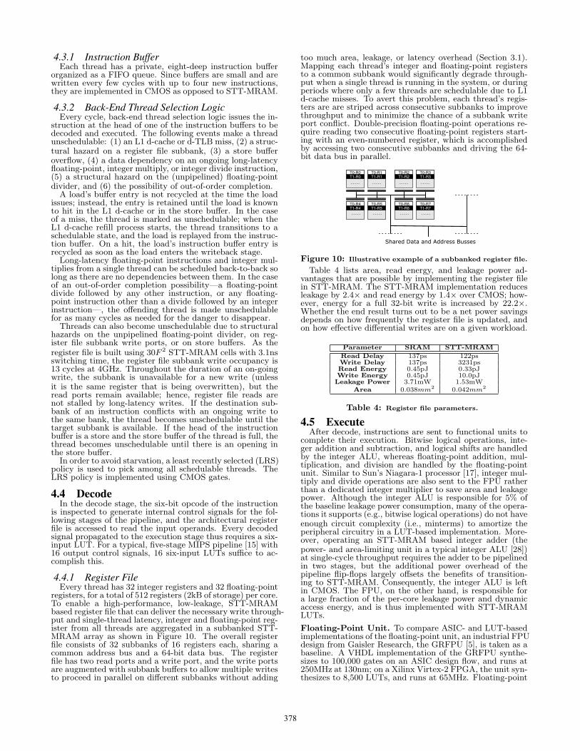
4.4.1 Register FileEvery thread has 32 integer registers and 32 floating-point
registers, for a total of 512 registers (2kB of storage) per core.To enable a high-performance, low-leakage, STT-MRAMbased register file that can deliver the necessary write through-put and single-thread latency, integer and floating-point reg-ister from all threads are aggregated in a subbanked STT-MRAM array as shown in Figure 10. The overall registerfile consists of 32 subbanks of 16 registers each, sharing acommon address bus and a 64-bit data bus. The registerfile has two read ports and a write port, and the write portsare augmented with subbank buffers to allow multiple writesto proceed in parallel on different subbanks without adding
too much area, leakage, or latency overhead (Section 3.1).Mapping each thread’s integer and floating-point registersto a common subbank would significantly degrade through-put when a single thread is running in the system, or duringperiods where only a few threads are schedulable due to L1d-cache misses. To avert this problem, each thread’s regis-ters are are striped across consecutive subbanks to improvethroughput and to minimize the chance of a subbank writeport conflict. Double-precision floating-point operations re-quire reading two consecutive floating-point registers start-ing with an even-numbered register, which is accomplishedby accessing two consecutive subbanks and driving the 64-bit data bus in parallel.
Shared Data and Address Busses
T0-R0 T0-R1 T0-R2 T0-R3
T0-R4 T0-R5 T0-R6 T0-R7
T1-R0 T1-R1 T1-R2 T1-R3
T1-R4 T1-R5 T1-R6 T1-R7
Figure 10: Illustrative example of a subbanked register file.
Table 4 lists area, read energy, and leakage power ad-vantages that are possible by implementing the register filein STT-MRAM. The STT-MRAM implementation reducesleakage by 2.4× and read energy by 1.4× over CMOS; how-ever, energy for a full 32-bit write is increased by 22.2×.Whether the end result turns out to be a net power savingsdepends on how frequently the register file is updated, andon how effective differential writes are on a given workload.
Parameter SRAM STT-MRAM
Read Delay 137ps 122psWrite Delay 137ps 3231psRead Energy 0.45pJ 0.33pJWrite Energy 0.45pJ 10.0pJLeakage Power 3.71mW 1.53mW
Area 0.038mm2 0.042mm2
Table 4: Register file parameters.
4.5 ExecuteAfter decode, instructions are sent to functional units to
complete their execution. Bitwise logical operations, inte-ger addition and subtraction, and logical shifts are handledby the integer ALU, whereas floating-point addition, mul-tiplication, and division are handled by the floating-pointunit. Similar to Sun’s Niagara-1 processor [17], integer mul-tiply and divide operations are also sent to the FPU ratherthan a dedicated integer multiplier to save area and leakagepower. Although the integer ALU is responsible for 5% ofthe baseline leakage power consumption, many of the opera-tions it supports (e.g., bitwise logical operations) do not haveenough circuit complexity (i.e., minterms) to amortize theperipheral circuitry in a LUT-based implementation. More-over, operating an STT-MRAM based integer adder (thepower- and area-limiting unit in a typical integer ALU [28])at single-cycle throughput requires the adder to be pipelinedin two stages, but the additional power overhead of thepipeline flip-flops largely offsets the benefits of transition-ing to STT-MRAM. Consequently, the integer ALU is leftin CMOS. The FPU, on the other hand, is responsible fora large fraction of the per-core leakage power and dynamicaccess energy, and is thus implemented with STT-MRAMLUTs.
Floating-Point Unit. To compare ASIC- and LUT-basedimplementations of the floating-point unit, an industrial FPUdesign from Gaisler Research, the GRFPU [5], is taken as abaseline. A VHDL implementation of the GRFPU synthe-sizes to 100,000 gates on an ASIC design flow, and runs at250MHz at 130nm; on a Xilinx Virtex-2 FPGA, the unit syn-thesizes to 8,500 LUTs, and runs at 65MHz. Floating-point
378
addition, subtraction, and multiplication are fully pipelinedand execute with a three-cycle latency; floating-point divi-sion is unpipelined and takes 16 cycles.
To estimate the required pipeline depth for an STT-MRAMLUT-based implementation of the GRFPU to operate at4GHz at 32nm, we use published numbers on configurablelogic block (CLB) delays on a Virtex-2 FPGA [2]. A CLBhas a LUT+MUX delay of 630ps and an interconnect delayof 1 to 2ns based on its placement, which corresponds to acritical path of six to ten CLB delays. For STT-MRAM, weassume a critical path delay of eight LUTs, which representsthe average of these two extremes. Assuming a bufferedsix-input STT-MRAM LUT delay of 130ps and a flip-flopsequencing overhead (tsetup + tC→Q) of 50ps, and conserva-tively assuming a perfectly-balanced pipeline for the base-line GRFPU, we estimate that the STT-MRAM implemen-tation would need to be pipelined eight times deeper thanthe original to operate at 4GHz, with floating-point addi-tion, subtraction, and multiplication latencies of 24 cycles,and an unpipelined, 64-cycle floating-point divide latency.When calculating leakage power, area, and access energy,we account for the overhead of the increased number of flip-flops due to this deeper pipeline (flip-flop power, area, andspeed are extracted from 32nm circuit simulations of thetopology used in the OSU standard cell library [29]). Wecharacterize and account for the impact of loading on anSTT-MRAM LUT when driving another LUT stage or aflip-flop via Cadence-Spectre circuit simulations.
To estimate pipeline depth for the CMOS implementationof the GRFPU running at 4GHz, we first scale the baseline250MHz frequency linearly from 130nm to 32nm, which cor-responds to an intrinsic frequency of 1GHz at 32nm. Thus,conservatively ignoring the sequencing overhead, to operateat 4GHz, the circuit needs to be pipelined 4× deeper, with12-cycle floating-point addition, subtraction, and multipli-cation latencies, and a 64-cycle, unpipelined floating-pointdivide. Estimating power for CMOS (100,000 gates) re-quires estimating dynamic and leakage power for an averagegate in a standard-cell library. We characterize the followingOSU standard cells using circuit simulations at 32nm, anduse their average to estimate power for the CMOS-basedGRFPU design: INVX2, NAND2X1, NAND3X1, BUFX2,BUFX4, AOI22X1, MUX2X1, DFFPOSX1, and XNORX1.
Table 5 shows the estimated leakage, dynamic energy, andarea of the GRFPU in both pure CMOS and STT-MRAM.The CMOS implementation uses 100, 000 gates whereas theSTT-MRAM implementation uses 8,500 LUTs. Althougheach CMOS gate has lower dynamic energy than a six-inputLUT, each LUT can replace 12 logic gates on average. This12× reduction in unit count results in an overall reductionof the total dynamic energy. Similarly, although each LUThas higher leakage than a CMOS gate, the cumulative leak-age of 8,500 LUTs reduces leakage by 4× over the combinedleakage of 100, 000 gates. Area, on the other hand, is com-parable due to the reduced unit count compensating for the5× higher area of each LUT and the additional bufferingrequired to cascade the LUTs. (Note that these area es-timates do not account for wiring overheads in either theCMOS or the STT-MRAM implementations.) In summary,the FPU is a good candidate to place in STT-MRAM sinceits high circuit complexity produces logic functions withmany minterms that require many CMOS gates to imple-ment, which is exactly when a LUT-based implementationis advantageous.
Parameter CMOS FPU STT-MRAM FPU
Dynamic Energy 36pJ 26.7pJLeakage Power 259mW 61mW
Area 0.22mm2 0.20mm2
Table 5: FPU parameters. Area estimates do not includewiring overhead.
4.6 MemoryIn the memory stage, load and store instructions access
the STT-MRAM based L1 d-cache and d-TLB. To simplify
the scheduling of stores and to minimize the performanceimpact of contention on subbank write ports, each threadis allocated a CMOS-based, eight-deep store buffer holdingin-flight store instructions.
4.6.1 Store BuffersOne problem that comes up when scheduling stores is the
possibility of a d-cache subbank conflict at the time thestore reaches the memory stage. Since stores require addresscomputation before their target d-cache subbank is known,thread selection logic cannot determine if a store will expe-rience a port conflict in advance. To address this problem,the memory stage of the pipeline includes a CMOS-based,private, eight-deep store buffer per thread. So long as athread’s store buffer is not full, the thread selection logic canschedule the store without knowing the destination subbank.Stores are dispatched into and issued from store buffers inFIFO order; store buffers also provide an associative searchport to support store-to-load forwarding, similar to Sun’sNiagara-1 processor. We assume relaxed consistency mod-els where special synchronization primitives (e.g., memoryfences in weak consistency, or acquire/release operations inrelease consistency) are inserted into store buffers, and thestore buffer enforces the semantics of the primitives whenretiring stores and when forwarding to loads. Since the L1d-cache supports a single write port (but multiple subbankbuffers), only a single store can issue per cycle. Store buffers,and the L1 refill queue contend for access to this shared re-source, and priority is determined based on a round-robinpolicy.
4.6.2 L1 Data Cache and TLBBoth the L1 d-cache and the d-TLB are implemented us-
ing STT-MRAM arrays. The d-cache is equipped with tworead ports (one for snooping, and one for the core) and awrite port shared among all subbanks. At the time a load is-sues, the corresponding thread is marked unschedulable andrecycling of the instruction buffer entry holding the load ispostponed until it is ascertained that the load will not expe-rience a d-cache miss. Loads search the store buffer of thecorresponding thread and access the L1 d-cache in parallel,and forward from the store buffer in the case of a hit. Ona d-cache miss, the thread is marked unschedulable, and istransitioned back to a schedulable state once the data ar-rives. To accommodate refills returning from the L2, theL1 has a 16-deep, CMOS-based refill queue holding incom-ing data blocks. Store buffers and the refill queue contendfor access to the two subbanks of the L1, and are givenaccess using a round-robin policy. Since the L1 is writtenfrequently, it is optimized for write throughput using 10F 2
Read Delay 344ps 236ps 369psWrite Delay 344ps 3331ps 3399psRead Energy 60pJ 31pJ 53pJWrite Energy 60pJ 109pJ 131pJLeakage Power 78.4mW 11.0mW 31.3mW
Area 0.54mm2 0.19mm2 0.39mm2
Table 6: L1 d-cache parameters.
Table 6 compares the power, area, and latency character-istics of two different STT-MRAM based L1 configurationsto a baseline, 32KB CMOS implementation. A capacity-equivalent, 32KB d-cache reduces access latency from twoclock cycles to one, and cuts down the read energy by 1.9×due to shorter interconnect lengths possible with the den-sity advantage of STT-MRAM. Leakage power is reducedby 7.1×, and area is reduced by 2.8×. An alternative, 64kBconfiguration requires 72% of the area of the CMOS base-line, but increases capacity by 2×; this configuration takestwo cycles to read, and delivers a 2.5× leakage reductionover CMOS.
379
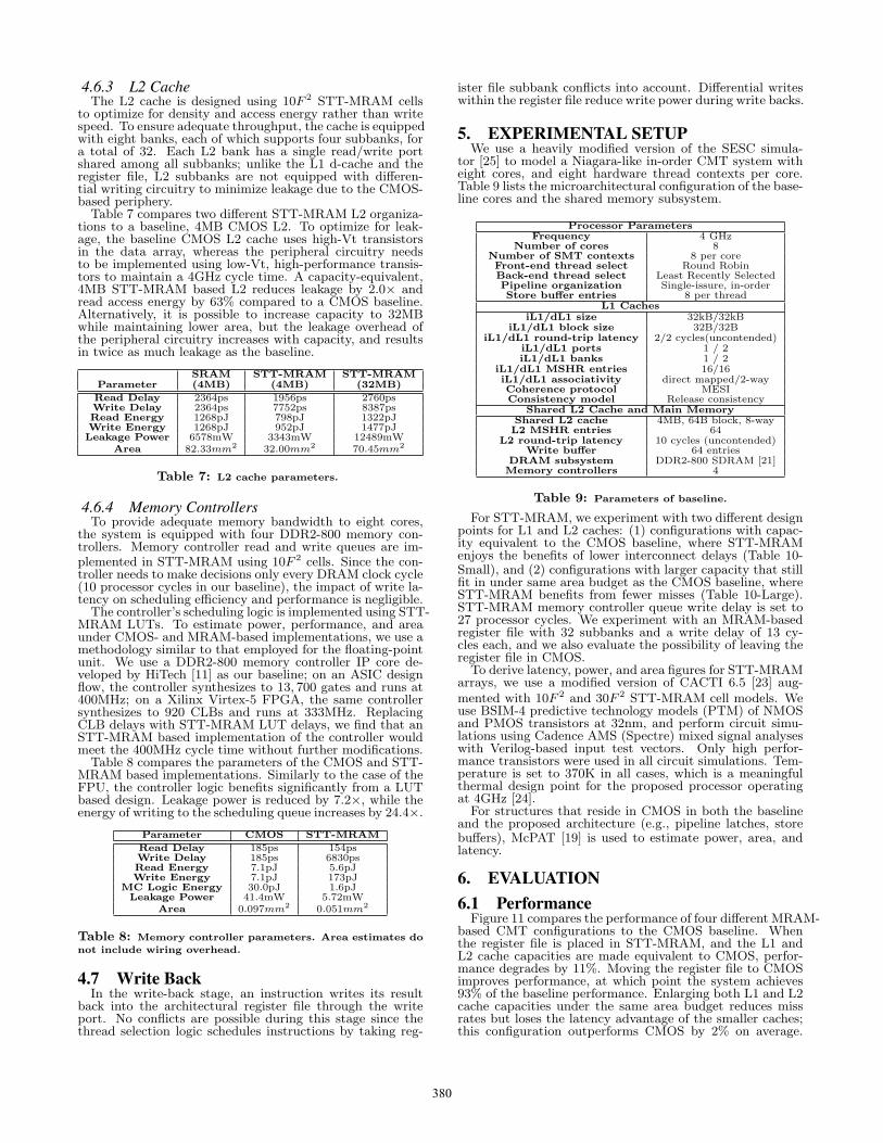
4.6.3 L2 CacheThe L2 cache is designed using 10F 2 STT-MRAM cells
to optimize for density and access energy rather than writespeed. To ensure adequate throughput, the cache is equippedwith eight banks, each of which supports four subbanks, fora total of 32. Each L2 bank has a single read/write portshared among all subbanks; unlike the L1 d-cache and theregister file, L2 subbanks are not equipped with differen-tial writing circuitry to minimize leakage due to the CMOS-based periphery.
Table 7 compares two different STT-MRAM L2 organiza-tions to a baseline, 4MB CMOS L2. To optimize for leak-age, the baseline CMOS L2 cache uses high-Vt transistorsin the data array, whereas the peripheral circuitry needsto be implemented using low-Vt, high-performance transis-tors to maintain a 4GHz cycle time. A capacity-equivalent,4MB STT-MRAM based L2 reduces leakage by 2.0× andread access energy by 63% compared to a CMOS baseline.Alternatively, it is possible to increase capacity to 32MBwhile maintaining lower area, but the leakage overhead ofthe peripheral circuitry increases with capacity, and resultsin twice as much leakage as the baseline.
Read Delay 2364ps 1956ps 2760psWrite Delay 2364ps 7752ps 8387psRead Energy 1268pJ 798pJ 1322pJWrite Energy 1268pJ 952pJ 1477pJLeakage Power 6578mW 3343mW 12489mW
Area 82.33mm2 32.00mm2 70.45mm2
Table 7: L2 cache parameters.
4.6.4 Memory ControllersTo provide adequate memory bandwidth to eight cores,
the system is equipped with four DDR2-800 memory con-trollers. Memory controller read and write queues are im-plemented in STT-MRAM using 10F 2 cells. Since the con-troller needs to make decisions only every DRAM clock cycle(10 processor cycles in our baseline), the impact of write la-tency on scheduling efficiency and performance is negligible.
The controller’s scheduling logic is implemented using STT-MRAM LUTs. To estimate power, performance, and areaunder CMOS- and MRAM-based implementations, we use amethodology similar to that employed for the floating-pointunit. We use a DDR2-800 memory controller IP core de-veloped by HiTech [11] as our baseline; on an ASIC designflow, the controller synthesizes to 13, 700 gates and runs at400MHz; on a Xilinx Virtex-5 FPGA, the same controllersynthesizes to 920 CLBs and runs at 333MHz. ReplacingCLB delays with STT-MRAM LUT delays, we find that anSTT-MRAM based implementation of the controller wouldmeet the 400MHz cycle time without further modifications.
Table 8 compares the parameters of the CMOS and STT-MRAM based implementations. Similarly to the case of theFPU, the controller logic benefits significantly from a LUTbased design. Leakage power is reduced by 7.2×, while theenergy of writing to the scheduling queue increases by 24.4×.
Parameter CMOS STT-MRAM
Read Delay 185ps 154psWrite Delay 185ps 6830psRead Energy 7.1pJ 5.6pJWrite Energy 7.1pJ 173pJ
MC Logic Energy 30.0pJ 1.6pJLeakage Power 41.4mW 5.72mW
Area 0.097mm2 0.051mm2
Table 8: Memory controller parameters. Area estimates donot include wiring overhead.
4.7 Write BackIn the write-back stage, an instruction writes its result
back into the architectural register file through the writeport. No conflicts are possible during this stage since thethread selection logic schedules instructions by taking reg-
ister file subbank conflicts into account. Differential writeswithin the register file reduce write power during write backs.
5. EXPERIMENTAL SETUPWe use a heavily modified version of the SESC simula-
tor [25] to model a Niagara-like in-order CMT system witheight cores, and eight hardware thread contexts per core.Table 9 lists the microarchitectural configuration of the base-line cores and the shared memory subsystem.
Processor ParametersFrequency 4 GHz
Number of cores 8Number of SMT contexts 8 per coreFront-end thread select Round RobinBack-end thread select Least Recently SelectedPipeline organization Single-issure, in-orderStore buffer entries 8 per thread
DRAM subsystem DDR2-800 SDRAM [21]Memory controllers 4
Table 9: Parameters of baseline.
For STT-MRAM, we experiment with two different designpoints for L1 and L2 caches: (1) configurations with capac-ity equivalent to the CMOS baseline, where STT-MRAMenjoys the benefits of lower interconnect delays (Table 10-Small), and (2) configurations with larger capacity that stillfit in under same area budget as the CMOS baseline, whereSTT-MRAM benefits from fewer misses (Table 10-Large).STT-MRAM memory controller queue write delay is set to27 processor cycles. We experiment with an MRAM-basedregister file with 32 subbanks and a write delay of 13 cy-cles each, and we also evaluate the possibility of leaving theregister file in CMOS.
To derive latency, power, and area figures for STT-MRAMarrays, we use a modified version of CACTI 6.5 [23] aug-mented with 10F 2 and 30F 2 STT-MRAM cell models. Weuse BSIM-4 predictive technology models (PTM) of NMOSand PMOS transistors at 32nm, and perform circuit simu-lations using Cadence AMS (Spectre) mixed signal analyseswith Verilog-based input test vectors. Only high perfor-mance transistors were used in all circuit simulations. Tem-perature is set to 370K in all cases, which is a meaningfulthermal design point for the proposed processor operatingat 4GHz [24].
For structures that reside in CMOS in both the baselineand the proposed architecture (e.g., pipeline latches, storebuffers), McPAT [19] is used to estimate power, area, andlatency.
6. EVALUATION6.1 Performance
Figure 11 compares the performance of four different MRAM-based CMT configurations to the CMOS baseline. Whenthe register file is placed in STT-MRAM, and the L1 andL2 cache capacities are made equivalent to CMOS, perfor-mance degrades by 11%. Moving the register file to CMOSimproves performance, at which point the system achieves93% of the baseline performance. Enlarging both L1 and L2cache capacities under the same area budget reduces missrates but loses the latency advantage of the smaller caches;this configuration outperforms CMOS by 2% on average.
Table 11: Simulated applications and their input sizes.
Optimizing the L2 for fewer misses (by increasing capacityunder a the same area budget) while optimizing the L1s forfast hits (by migrating to a denser, STT-MRAM cache withsame capacity) delivers similar results.
In general, performance bottlenecks are application de-pendent. For applications like CG, FFT and WATER, theMRAM-based register file represents the biggest performancehurdle. These applications encounter a higher number ofsubbank conflicts than others, and when the register file ismoved to CMOS, their performance improves significantly.EQUAKE, KMEANS, MG, and RADIX are found sensi-tive to floating-point instruction latencies as they encountermany stalls due to dependents of long-latency floating-pointinstructions in the 24-cycle, STT-MRAM based floating-point pipeline. CG, CHOLESKY, FFT, RADIX, and SWIMbenefit most from increasing cache capacities under the samearea budget as CMOS, by leveraging the density advantageof STT-MRAM.
6.2 PowerFigure 12 compares total power dissipation across all five
systems. STT-MRAM configurations that maintain the samecache sizes as CMOS reduce total power by 1.7× over CMOS.Despite their higher performance potential, configurationswhich increase cache capacity under the same area budgetincrease power by 1.2× over CMOS, due to the significantamount of leakage power dissipated in the CMOS-based de-coding and sensing circuitry in the 32MB L2 cache. Al-though a larger L2 can reduce write power by allowing forfewer L2 refills and writes to memory controllers’ schedulingqueues, the increased leakage power consumed by the pe-ripheral circuitry outweighs the savings on dynamic power.
Figure 13 shows the breakdown of leakage power acrossdifferent components for all evaluated systems. Total leak-age power is reduced by 2.1× over CMOS when cache ca-pacities are kept the same. Systems with a large L2 cacheincrease leakage power by 1.3× due to the CMOS-based pe-riphery. The floating-point units, which consume 18% of thetotal leakage power in the CMOS baseline, benefit signifi-cantly from an STT-MRAM based implementation. STT-MRAM based L1 caches and TLBs together reduce leakagepower by another 10%. The leakage power of the memorycontrollers in STT-MRAM is negligible, whereas in CMOSit is 1.5%.
11.40
5.32 5.34
14.92 14.48
0
2
4
6
8
10
12
14
CMOS Small L1 and L2, STT-‐MRAM
RF
Small L1 and L2, CMOS RF
Large L1 and L2, CMOS RF
Small L1, Large L2, CMOS RF
Leakage Po
wer (W
)
RF
FPU
ALU and Bypass
InstBuf and STQ
FFs and Comb Logic
L1s and TLBs
L2
MC
Figure 13: Leakage Power.
7. RELATED WORKSTT-MRAM has received increasing attention in recent
years at the device and circuit levels [8,12,26,32,33,37,39].At the architecture level, Desikan et al. [9] explore usingMRAM as a DRAM replacement to improve memory band-width and latency. Dong et al. [10] explore 3D-stackedMRAM, and propose a model to estimate the power and areaof MRAM arrays. Sun et al. [30] present a read-preemptivewrite technique which allows an SRAM-MRAM hybrid L2
381
cache to get performance improvements and power reduc-tions. Zhou et al. [40] apply an early write terminationtechnique at the circuit level to reduce STT-MRAM writeenergy. Wu et al. [34] propose a data migration scheme toa hybrid cache architecture to reduce the number of writesto resistive memories. Xu et al. [36] propose a circuit tech-nique, which sizes transistors smaller than the worst casesize required to generate the switching current to improvedensity. Most of this earlier work on MRAM considers itas a DRAM or SRAM cache replacement in the system andnone of them discusses how to use resistive memories to buildcombinational logic.
8. CONCLUSIONSIn this paper, we have presented a new technique that re-
duces leakage and dynamic power in a deep-submicron mi-croprocessor by migrating power- and performance-criticalhardware resources from CMOS to STT-MRAM. We haveevaluated the power and performance impact of implement-ing on-chip caches, register files, memory controllers, floating-point units, and various combinational logic blocks usingmagnetoresistive circuits, and we have explored the criticalissues that affect whether a RAM array or a combinationallogic block can be effectively implemented in MRAM. Wehave observed significant gains in power-efficiency by par-titioning on-chip hardware resources among STT-MRAMand CMOS judiciously to exploit the unique power, area,and speed benefits of each technology, and by carefully re-architecting the pipeline to mitigate the performance impactof long write latencies and high write power.
We believe this paper is part of an exciting new trend to-ward leveraging resistive memories in effecting a significantleap in the performance and efficiency of computer systems.
9. ACKNOWLEDGMENTSThe authors would like to thank Yanwei Song, Ravi Patel,
Sheng Li, and Todd Austin for useful feedback.
10. REFERENCES[1] V. Agarwal, M. Hrishikesh, S. Keckler, and D. Burger. Clock
rate vs. IPC: End of the road for conventional microprocessors.In International Symposium on Computer Architecture,Vancouver, Canada, June 2000.
[2] ALTERA. Stratix vs. Virtex-2 Pro FPGA performanceanalysis, 2004.
[3] B. Amrutur and M. Horowitz. Speed and power scaling ofSRAMs. 2000.
[4] D. Burger, J. R. Goodman, and A. Kagi. Memory bandwidthlimitations of future microprocessors. In InternationalSymposium on Computer Architecture, Philedelphia, PA, May1996.
[5] E. Catovic. GRFPU-high performance IEEE-754 floating-pointunit. http://www.gaisler.com/doc/grfpu_dasia.pdf.
[6] C. Chappert, A. Fert, and F. N. V. Dau. The emergence ofspin electronics in data storage. Nature Materials, 6:813–823,November 2007.
[7] M. D. Ciletti. Advanced Digital Design with the Verilog HDL.2004.
[8] D. Suzuki et al. Fabrication of a nonvolatile lookup tablecircuit chip using magneto/semiconductor hybrid structure foran immediate power up field programmable gate array. InSymposium on VLSI Circuits, 2009.
[9] R. Desikan, C. R. Lefurgy, S. W. Keckler, and D. C. Burger.On-chip MRAM as a high-bandwidth, low-latency replacementfor DRAM physical memories. In IBM Austin Center forAdvanced Studies Conference, 2003.
[10] X. Dong, X. Wu, G. Sun, H. Li, Y. Chen, and Y. Xie. Circuitand mircoarchitecture evaluation of 3D stacking magneticRAM (MRAM) as a universal memory replacement. In DesignAutomation Conference, 2008.
[11] HiTech. DDR2 memory controller IP core for FPGA and ASIC.http://www.hitechglobal.com/IPCores/DDR2Controller.htm.
[12] Y. Huai. Spin-transfer torque MRAM (STT-MRAM) challengesand prospects. AAPPS Bulletin, 18(6):33–40, December 2008.
[13] ITRS. International Technology Roadmap forSemiconductors: 2009 Executive Summary.http://www.itrs.net/Links/2009ITRS/Home2009.htm.
[14] K. Tsuchida et al. A 64Mb MRAM with clamped-reference andadequate-reference schemes. In Proceedings of the IEEEInternational Solid-State Circuits Conference, 2010.
[15] G. Kane. MIPS RISC Architecture. 1988.
[16] U. R. Karpuzcu, B. Greskamp, and J. Torellas. Thebubblewrap many-core: Popping cores for sequentialacceleration. In International Symposium onMicroarchitecutre, 2009.
[17] P. Kongetira, K. Aingaran, and K. Olukotun. Niagara: A32-way multithreaded sparc processor. IEEE Micro,25(2):21–29, 2005.
[18] B. Lee, E. Ipek, O. Mutlu, and D. Burger. Architectingphase-change memory as a scalable dram alternative. InInternational Symposium on Computer Architecture, Austin,TX, June 2009.
[19] S. Li, J. H. Ahn, R. D. Strong, J. B. Brockman, D. M. Tullsen,and N. P. Jouppi. McPAT: An integrated power, area, andtiming modeling framework for multicore and manycorearchitectures. In International Symposium on ComputerArchitecture, 2009.
[20] M. Hosomi and H. Yamagishi and T. Yamamoto and K. Besshaet al. A novel nonvolatile memory with spin torque transfermagnetization switching: Spin-RAM. In IEDM TechnicalDigest, pages 459–462, 2005.
[21] Micron. 512Mb DDR2 SDRAM Component Data Sheet:MT47H128M4B6-25, March 2006. http://download.micron.com/pdf/datasheets/dram/ddr2/512MbDDR2.pdf.
[22] N. Muralimanohar, R. Balasubramonian, and N. Jouppi.Optimizing NUCA organizations and wiring alternatives forlarge caches with CACTI 6.0. Chicago, IL, Dec. 2007.
[23] N. Muralimanohar, R. Balasubramonian, and N. P. Jouppi.NAS parallel benchmarks. Technical report, NASA AmesResearch Center, March 1994. Tech. Rep. RNR-94-007.
[24] U. G. Nawathe, M. Hassan, K. C. Yen, A. Kumar,A. Ramachandran, and D. Greenhill. Implementation of an8-core, 64-thread, power-efficient sparc server on a chip. IEEEJournal of Solid-State Circuits, 43(1):6–20, January 2008.
[25] J. Renau, B. Fraguela, J. Tuck, W. Liu, M. Prvulovic, L. Ceze,S. Sarangi, P. Sack, K. Strauss, and P. Montesinos. SESCsimulator, January 2005. http://sesc.sourceforge.net.
[26] S. Matsunaga et al. Fabrication of a nonvolatile full adderbased on logic-in-memory architecture using magnetic tunneljunctions. Applied Physics Express, 1(9), 2008.
[27] S. Rusu et al. A 45nm 8-Core Enterprise Xeon Processor. InProceedings of the IEEE International Solid-State CircuitsConference, pages 56–57, Feb. 2009.
[28] Sanu K. Mathew and Mark A. Anders and Brad Bloechel et al.A 4-GHz 300-mW 64-bit integer execution ALU with dualsupply voltages in 90-nm CMOS. IEEE Journal of Solid-StateCircuits, 40(1):44–51, January 2005.
[29] J. E. Stine, I. Castellanos, M. Wood, J. Henson, and F. Love.Freepdk: An open-source variation-aware design kit. InInternational Conference on Microelectronic SystemsEducation, 2007.http://vcag.ecen.okstate.edu/projects/scells/.
[30] G. Sun, X. Dong, Y. Xie, J. Li, and Y. Chen. A novel 3Dstacked MRAM cache architecture for CMPs. InHigh-Performance Computer Architecture, 2009.
[31] T. Kawahara et al. 2 Mb SPRAM (spin-transfer torque RAM)with bit-by-bit bi-directional current write andparallelizing-direction current read. IEEE Journal ofSolid-State Circuits, 43(1):109–120, January 2008.
[32] T. Kishi and H. Yoda and T. Kai et al. Lower-current and fastswitching of a perpendicular TMR for high speed and highdensity spin-transfer-torque MRAM. In IEEE InternationalElectron Devices Meeting, 2008.
[33] U. K. Klostermann et al. A perpendicular spin torqueswitching based MRAM for the 28 nm technology node. InIEEE International Electron Devices Meeting, 2007.
[34] X. Wu, J. Li, L. Zhang, E. Speight, R. Rajamony, and Y. Xie.Hybrid cache architecture with disparate memory technologies.In International Symposium on Computer Architecture, 2009.
[35] Xilinx. Virtex-6 FPGA Family Overview, November 2009.http://www.xilinx.com/support/documentation/data_sheets/ds150.pdf.
[36] W. Xu, Y. Chen, X. Wang, and T. Zhang. Improving STTMRAM storage density through smaller-than-worst-casetransistor sizing. In Design Automation Conference, 2009.
[37] W. Xu, T. Zhang, and Y. Chen. Spin-transfer torquemagnetoresistive content addressable memory (CAM) cellstructure design with enhanced search noise margin. InInternational Symposium on Circuits and Systems, 2008.
[38] W. Zhao and Y. Cao. New generation of predictive technologymodel for sub-45nm design exploration. In InternationalSymposium on Quality Electronic Design, 2006.http://ptm.asu.edu/.
[39] W. Zhao, C. Chappert, and P. Mazoyer. Spin transfer torque(STT) MRAM-based runtime reconfiguration FPGA circuit. InACM Transactions on Embedded Computing Systems, 2009.
[40] P. Zhou, B. Zhao, J. Yang, and Y. Zhang. Energy reduction forSTT-RAM using early write termination. In InternationalConference on Computer-Aided Design, 2009.