RESISTIVE HUMIDITY SENSOR MADE FROM PALM-OIL-DERIVED GRAPHENE FILM WAI YIN LING A project report submitted in partial fulfilment of the requirements for the award of the degree of Master of Engineering (Electrical - Computer Microelectronics System) Faculty of Electrical Engineering Universiti Teknologi Malaysia JUNE 2015
Transcript
RESISTIVE HUMIDITY SENSOR MADE FROM PALM-OIL-DERIVED
GRAPHENE FILM
WAI YIN LING
A project report submitted in partial fulfilment of the
requirements for the award of the degree of
Master of Engineering (Electrical - Computer Microelectronics System)
Faculty of Electrical Engineering
Universiti Teknologi Malaysia
JUNE 2015
iii
ACKNOWLEDGEMENT
In preparing this project report, I was in contact with many people, researchers,
academicians, and practitioners. They have contributed towards my understanding and
thoughts. In particular, I wish to express my sincere appreciation to my main project
supervisor, Dr. Shaharin Fadzli Abd Rahman, for encouragement, guidance, critics and
friendship.
My sincere appreciation also extends to all my colleagues and others who have
provided assistance at various occasions. Their views and tips are useful indeed.
Unfortunately, it is not possible to list all of them in this limited space. I am grateful
to all my family members.
iv
ABSTRACT
Graphene is known to be highly conductive and sensitive to adsorbed
molecules thus make it suitable for sensor application. The astonishing properties of
graphene attracted the attention to develop ultra-high sensitive sensor with very fast
response and recovery time. In this project, a resistive humidity sensor which utilizes
graphene as the sensing area has been fabricated and characterized. Different types of
graphene samples (i.e. single-layer graphene on copper substrate, single-layer
graphene on nickel substrate synthesized using thermal CVD, multi-layers graphene
on nickel substrate synthesized using thermal CVD) were used in this project to further
investigate the effect of crystallinity of the graphene on its sensing behavior. In order
to fabricate the sensor device, the 2-terminals and 4-terminals electrodes configuration
was chosen. Sensor fabrication process includes photolithography, copper etching and
graphene transfer process. Current-voltage measurement of the fabricated is performed
at different relative humidity inside dry box. The result of the resistance of the
graphene sample responding towards the change of relative humidity shows an inverse
exponential association. Measurement result for different type of graphene are
compared to assess the relationship between the crystallinity and sensor performance.
v
ABSTRAK
Grafin diketahui sebagai sangat konduktif dan sensitif terhadap molekul yang
terjerap padanya. Dengan itu menjadikannya sesuai untuk aplikasi sensor. Ciri-ciri
menakjubkan grafin menarik perhatian untuk penghasilan sensor sensitif ultra tinggi
dengan masa tindak balas dan pemulihan yang cepat. Dalam projek ini, sensor
kelembapan berdasarkan rintangan yang menggunakan grafin sebagai bahagian deria,
telah direka dan dicirikan. Tiga jenis grafin yang dihasilkan menggunakan teknik
pemendapan berhaba wap kimia (iaitu lapisan tunggal grafin pada substrat tembaga,
lapisan tunggal grafin pada substrat nikel dan pelbagai lapisan grafin pada substrat
nikel), telah digunakan dalam projek ini untuk menyiasat kesan tahap penghabluran
grafin pada operasi sensor. 2-terminal dan 4-terminal konfigurasi elektrod dipilih
sebagai struktur peranti. Proses fabrikasi sensor termasuk fotolitografi, penghakisan
tembaga dan proses pemindahan graphene. Pengukuran arus voltan dilakukan pada
kelembapan yang berbeza di dalam kotak kering. Gerak balas rintangan sampel
graphene terhadap perubahan kelembapan relatif menunjukkan hubungan eksponen
songsang. Hasil pengukuran bagi grafin yang berbeza jenis dibandingkan untuk
menilai hubungan antara penghabluran dan prestasi sensor.
vi
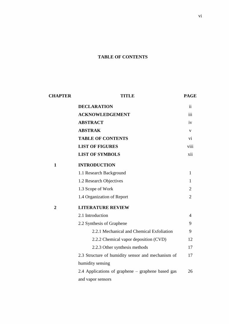
TABLE OF CONTENTS
CHAPTER TITLE PAGE
DECLARATION ii
ACKNOWLEDGEMENT iii
ABSTRACT iv
ABSTRAK v
TABLE OF CONTENTS vi
LIST OF FIGURES viii
LIST OF SYMBOLS xii
1 INTRODUCTION
1.1 Research Background 1
1.2 Research Objectives 1
1.3 Scope of Work 2
1.4 Organization of Report 2
2 LITERATURE REVIEW
2.1 Introduction 4
2.2 Synthesis of Graphene 9
2.2.1 Mechanical and Chemical Exfoliation 9
2.2.2 Chemical vapor deposition (CVD) 12
2.2.3 Other synthesis methods 17
2.3 Structure of humidity sensor and mechanism of
humidity sensing
17
2.4 Applications of graphene – graphene based gas
and vapor sensors
26
vii
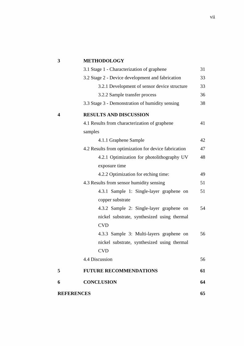
3 METHODOLOGY
3.1 Stage 1 - Characterization of graphene 31
3.2 Stage 2 - Device development and fabrication 33
3.2.1 Development of sensor device structure 33
3.2.2 Sample transfer process 36
3.3 Stage 3 - Demonstration of humidity sensing 38
4 RESULTS AND DISCUSSION
4.1 Results from characterization of graphene
samples
41
4.1.1 Graphene Sample 42
4.2 Results from optimization for device fabrication 47
4.2.1 Optimization for photolithography UV
exposure time
48
4.2.2 Optimization for etching time: 49
4.3 Results from sensor humidity sensing 51
4.3.1 Sample 1: Single-layer graphene on
copper substrate
51
4.3.2 Sample 2: Single-layer graphene on
nickel substrate, synthesized using thermal
CVD
54
4.3.3 Sample 3: Multi-layers graphene on
nickel substrate, synthesized using thermal
CVD
56
4.4 Discussion 56
5 FUTURE RECOMMENDATIONS 61
6 CONCLUSION 64
REFERENCES 65
viii
LIST OF FIGURES
FIGURE NO. TITLE PAGE
2.1 Forms of sp2-bonded carbon. (A) Fullerene, (B) single-