23
RESISTIVE MEMORY TECHNOLOGY CS/ECE 7810: Advanced Computer Architecture Mahdi Nazm Bojnordi Assistant Professor School of Computing University of Utah
RESISTIVE MEMORY TECHNOLOGY
CS/ECE 7810: Advanced Computer Architecture
Mahdi Nazm Bojnordi
Assistant Professor
School of Computing
University of Utah

Overview
¨ Upcoming deadlines¤ April 7th: Sign up for your student paper presentation
¨ This lecture¤ Resistive memory technology¤ Write optimization techniques¤ Wear leveling¤ MLC technologies

Resistive Memory Technology
¨ Main benefits¤ Non-volatile memory¤ Multi-level storage¤ Denser cells¤ Better scalability
¨ Shortcomings¤ Limited endurance¤ High switching delay and energy
What can we do?
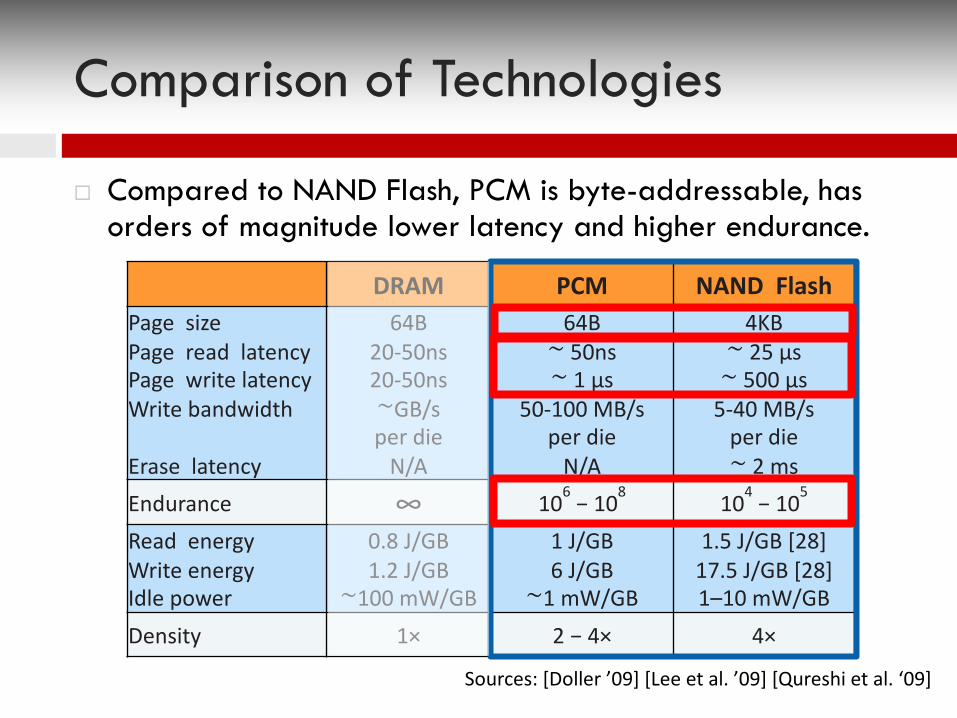
Comparison of Technologies
¨ Compared to NAND Flash, PCM is byte-addressable, has orders of magnitude lower latency and higher endurance.
DRAM PCM NAND FlashPage sizePage read latency Page write latencyWrite bandwidth
Erase latency
64B20-50ns20-50ns∼GB/s per die
N/A
64B∼ 50ns∼ 1 µs
50-100 MB/s per die
N/A
4KB∼ 25 µs∼ 500 µs
5-40 MB/s per die∼ 2 ms
Endurance ∞ 106 − 108 104 − 105
Read energyWrite energyIdle power
0.8 J/GB1.2 J/GB
∼100 mW/GB
1 J/GB6 J/GB
∼1 mW/GB
1.5 J/GB [28]17.5 J/GB [28]1–10 mW/GB
Density 1× 2 − 4× 4×
Sources: [Doller ’09] [Lee et al. ’09] [Qureshi et al. ‘09]
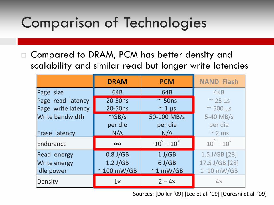
Comparison of Technologies
¨ Compared to DRAM, PCM has better density and scalability and similar read but longer write latencies
Sources: [Doller ’09] [Lee et al. ’09] [Qureshi et al. ‘09]
DRAM PCM NAND FlashPage sizePage read latency Page write latencyWrite bandwidth
Erase latency
64B20-50ns20-50ns∼GB/s per die
N/A
64B∼ 50ns∼ 1 µs
50-100 MB/s per die
N/A
4KB∼ 25 µs∼ 500 µs
5-40 MB/s per die∼ 2 ms
Endurance ∞ 106 − 108 104 − 105
Read energyWrite energyIdle power
0.8 J/GB1.2 J/GB
∼100 mW/GB
1 J/GB6 J/GB
∼1 mW/GB
1.5 J/GB [28]17.5 J/GB [28]1–10 mW/GB
Density 1× 2 − 4× 4×

Latency Comparison
10ns 100ns 1us 10us 100us 1ms 10ms
NA
ND
Fla
sh
PCM
DRA
M
Har
d D
isk
NA
ND
Fla
sh
PCM
DRA
M
Har
d D
isk
Read
Write[Qureshi’09]
0 1 0 1 1 0 1 1 0 1 1 0 1 1 1 0
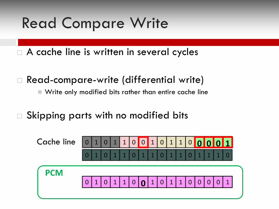
Read Compare Write
0 1 0 1 1 0 0 1 0 1 1 0 0 0 0 10 1 0 1 1 0 1 1 0 1 1 0 1 1 1 0
PCM0 1 0 1 1 0 0 1 0 1 1 0 0 0 0 10 0 0 0 1
Cache line
¨ A cache line is written in several cycles
¨ Read-compare-write (differential write)n Write only modified bits rather than entire cache line
¨ Skipping parts with no modified bits
0 1 0 1 0 1
1 0 1 0 1 0
1 0 1 0 1 1
1 0 1 0 1 0
0 1 0 1 0 1
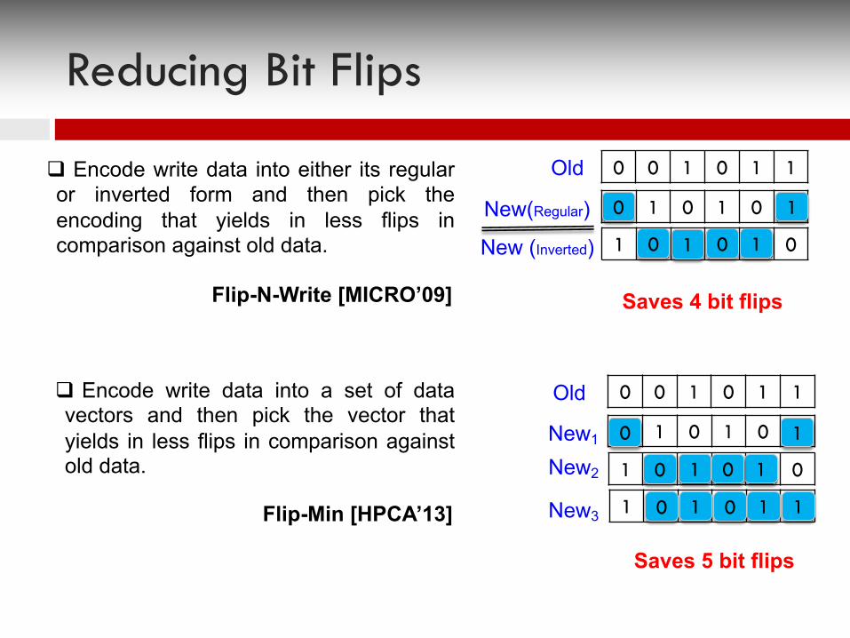
q Encode write data into either its regularor inverted form and then pick theencoding that yields in less flips incomparison against old data.
0 0 1 0 1 1Old
New(Regular)
New (Inverted)
Saves 4 bit flips
q Encode write data into a set of datavectors and then pick the vector thatyields in less flips in comparison againstold data.
0 0 1 0 1 1Old
New1
New2
Saves 5 bit flips
New3
0 1
1 100
11 10
10
10
01
0
Reducing Bit Flips
Flip-N-Write [MICRO’09]
Flip-Min [HPCA’13]
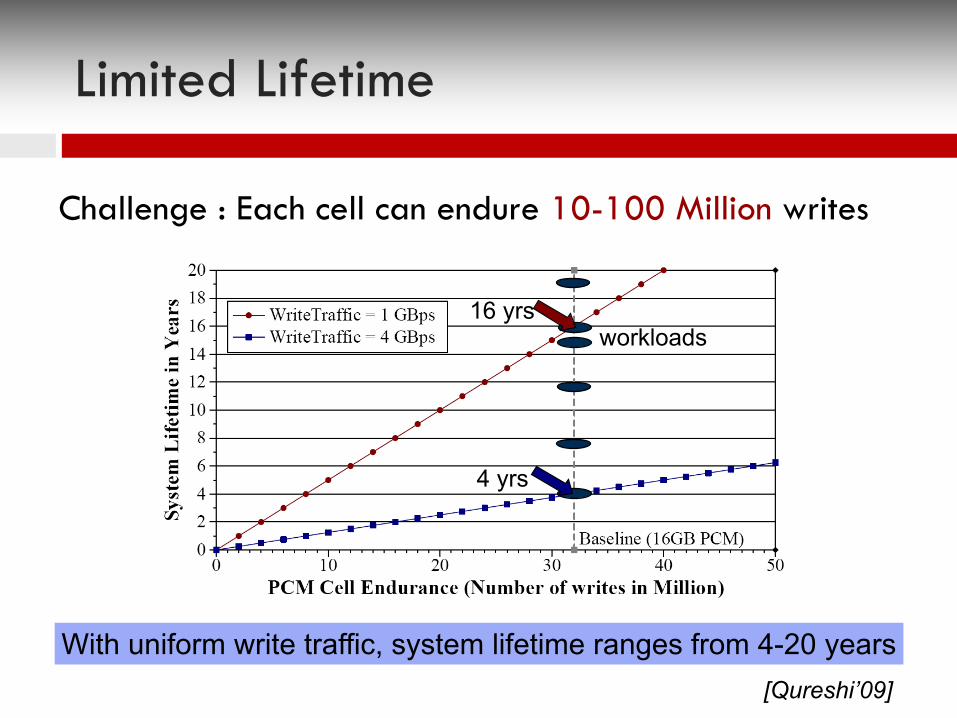
Challenge : Each cell can endure 10-100 Million writes
With uniform write traffic, system lifetime ranges from 4-20 years
workloads16 yrs
4 yrs
Limited Lifetime
[Qureshi’09]
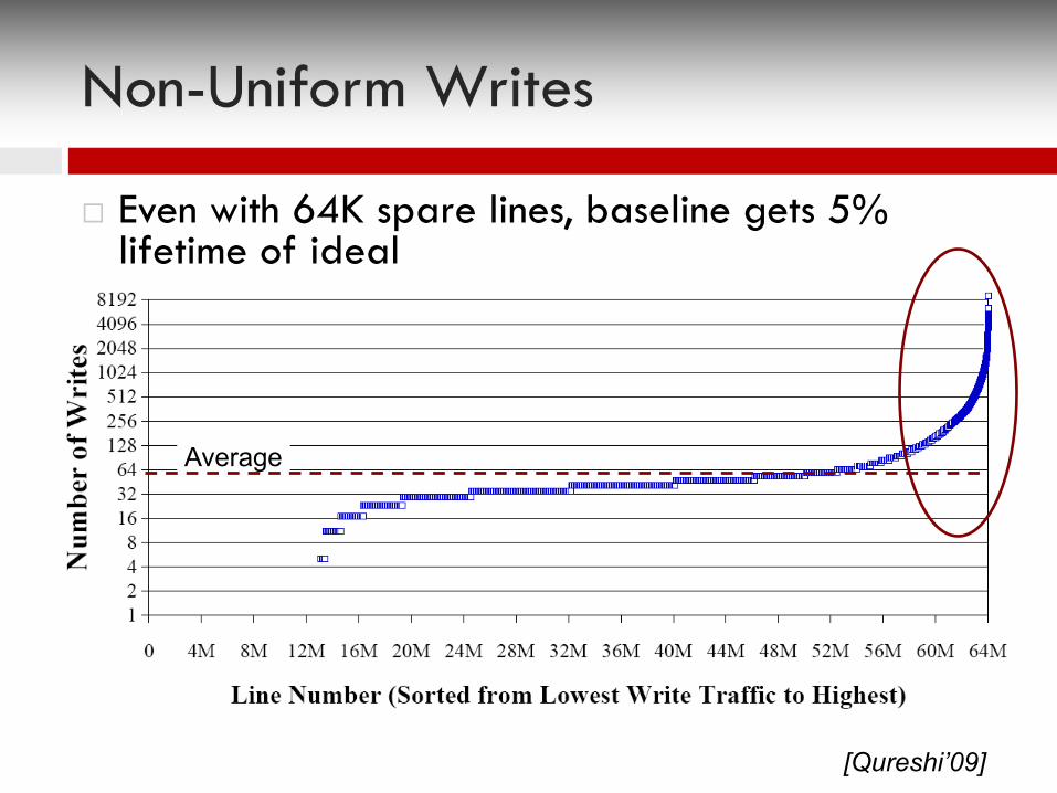
Non-Uniform Writes
¨ Even with 64K spare lines, baseline gets 5% lifetime of ideal
Average
[Qureshi’09]

Impact of Non-Uniformity
¨ Even with 64K spare lines, baseline gets 5% lifetime of ideal
20x lower
Num. writes before system failureNum. writes before failure with uniform writesNorm. Endurance = x 100%
05101520253035404550556065707580859095100
oltp db1 db2 fft stride stress Gmean
Norm
aliz
ed E
ndur
ance
(%)
Baseline w/o sparesBaseline (64K spare lines)
[Qureshi’09]

Making Writes Uniform
¨ Wear Leveling: make writes uniform by remapping frequently written lines
Line Addr. Lifetime Count Period CountA 99K (Low) 1K (Low)B 100K (Med) 3K (High)C 101K (High) 2K (Med)
è
Line Remap AddrA CB AC B
Indirection Table
Physical Address PCM Address
[Qureshi’09]
How to Remap
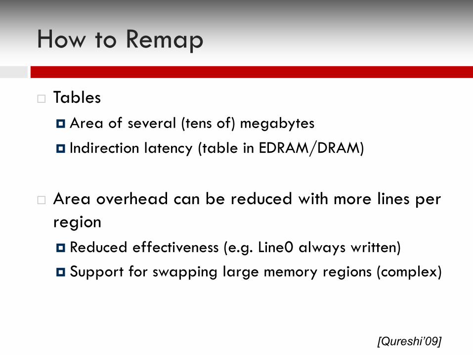
¨ Tables¤ Area of several (tens of) megabytes¤ Indirection latency (table in EDRAM/DRAM)
¨ Area overhead can be reduced with more lines per region¤ Reduced effectiveness (e.g. Line0 always written)¤ Support for swapping large memory regions (complex)
[Qureshi’09]
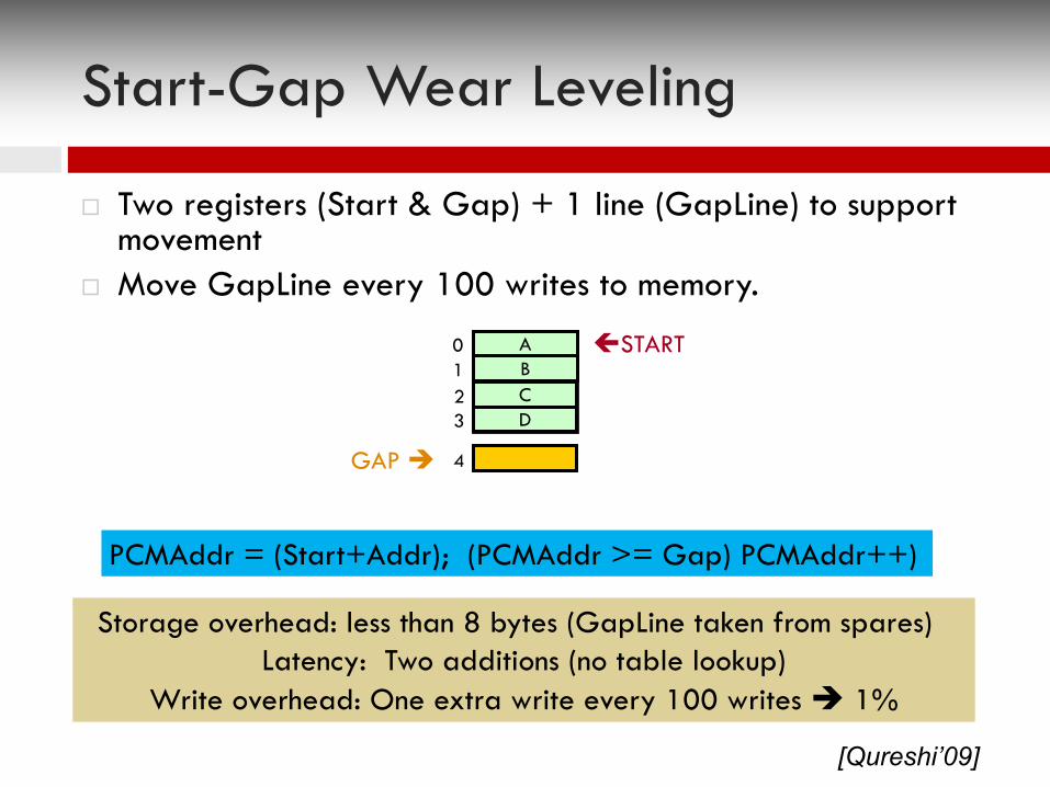
Start-Gap Wear Leveling
¨ Two registers (Start & Gap) + 1 line (GapLine) to support movement
¨ Move GapLine every 100 writes to memory.
çSTARTABC
0123
4
PCMAddr = (Start+Addr); (PCMAddr >= Gap) PCMAddr++)
D
GAP è
Storage overhead: less than 8 bytes (GapLine taken from spares) Latency: Two additions (no table lookup)
Write overhead: One extra write every 100 writes è 1%
[Qureshi’09]
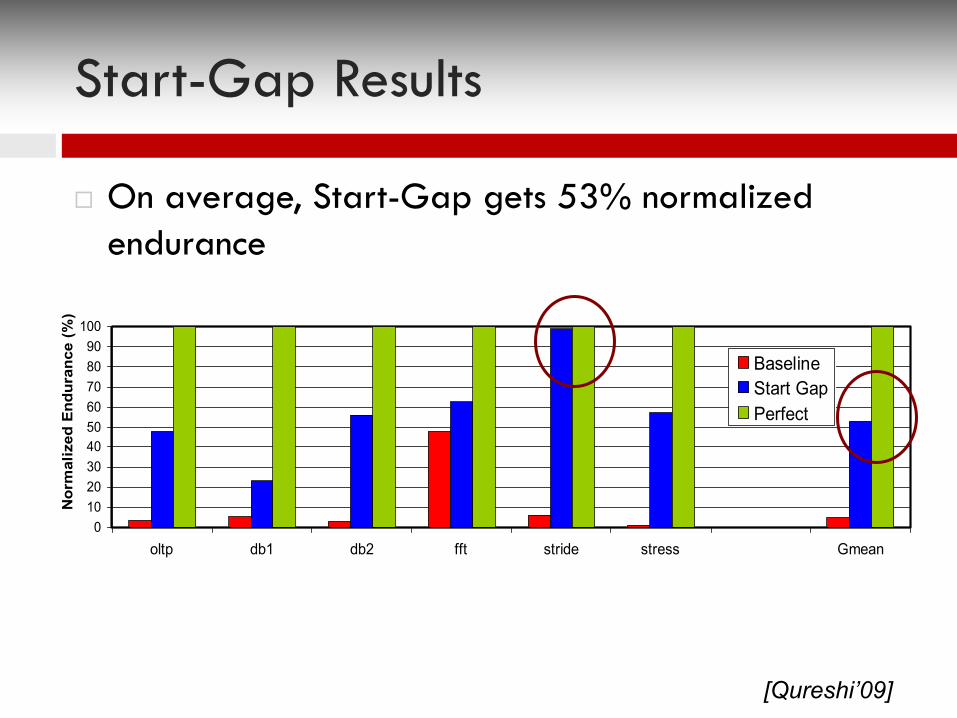
Start-Gap Results
¨ On average, Start-Gap gets 53% normalized endurance
0102030405060708090
100
oltp db1 db2 fft stride stress Gmean
Nor
mal
ized
End
uran
ce (%
)
BaselineStart GapPerfect
[Qureshi’09]
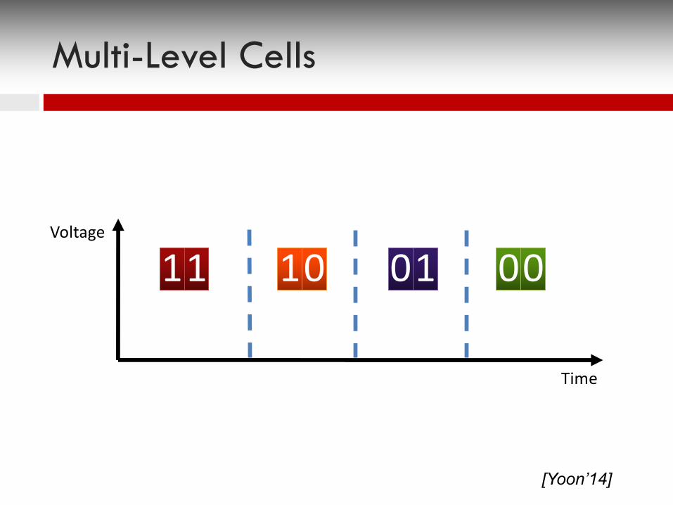
Multi-Level Cells
Voltage
Time
11 000110
[Yoon’14]
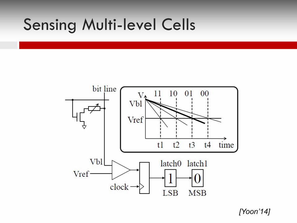
Sensing Multi-level Cells
[Yoon’14]

Voltage
Time
11 000110
Multi-Level Cells
[Yoon’14]
Voltage
Time
11 000110
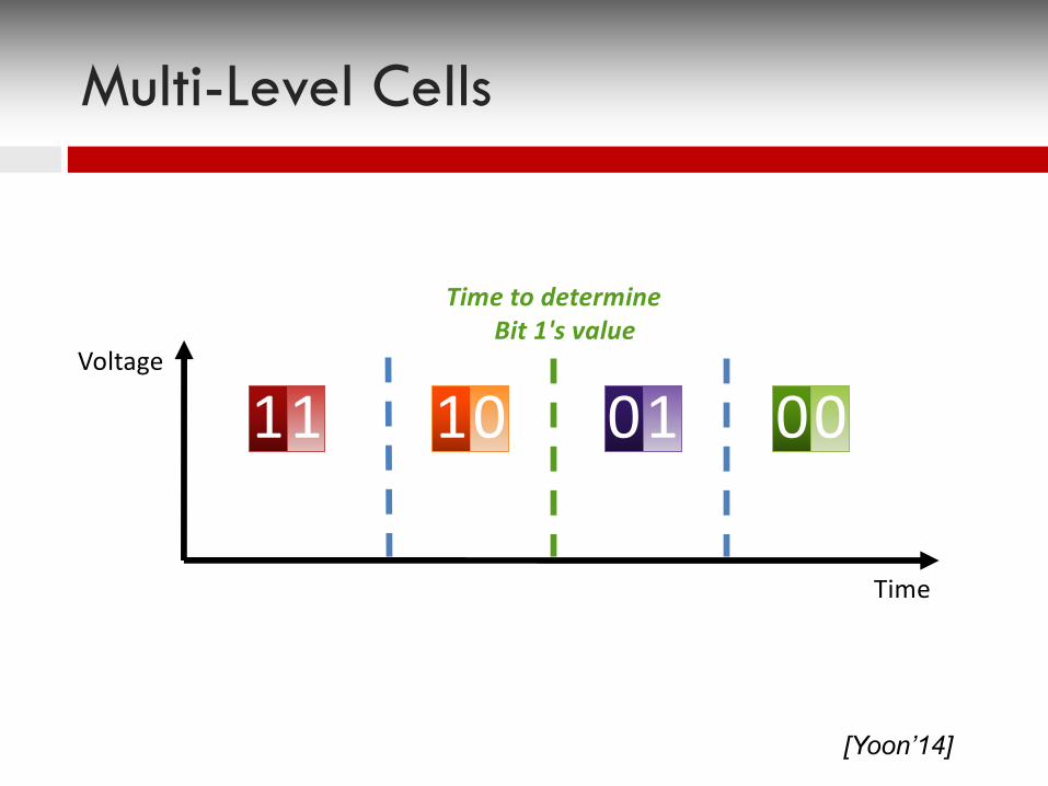
Time to determine Bit 1's value
Multi-Level Cells
[Yoon’14]
Voltage
Time
11 000110
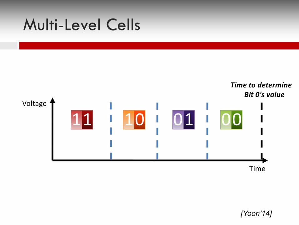
Time to determine Bit 0's value
Multi-Level Cells
[Yoon’14]
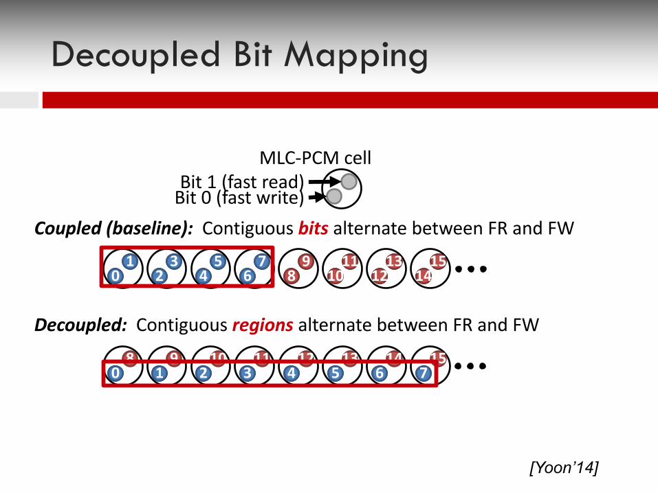
MLC-PCM cellBit 1 (fast read)
Bit 0 (fast write)
Decoupled Bit Mapping
bit
bit
bit
bit
bit
bit
bit
bit
bit
bit
bit
bit
bit
bit
bit
bit
01
23
45
67
89
1011
1213
1415
Coupled (baseline): Contiguous bits alternate between FR and FW
12 13 14 158 9 10 11bit bit bit bit bit bit bit bit0 1 2 3 4 5 6 7
Decoupled: Contiguous regions alternate between FR and FW
[Yoon’14]
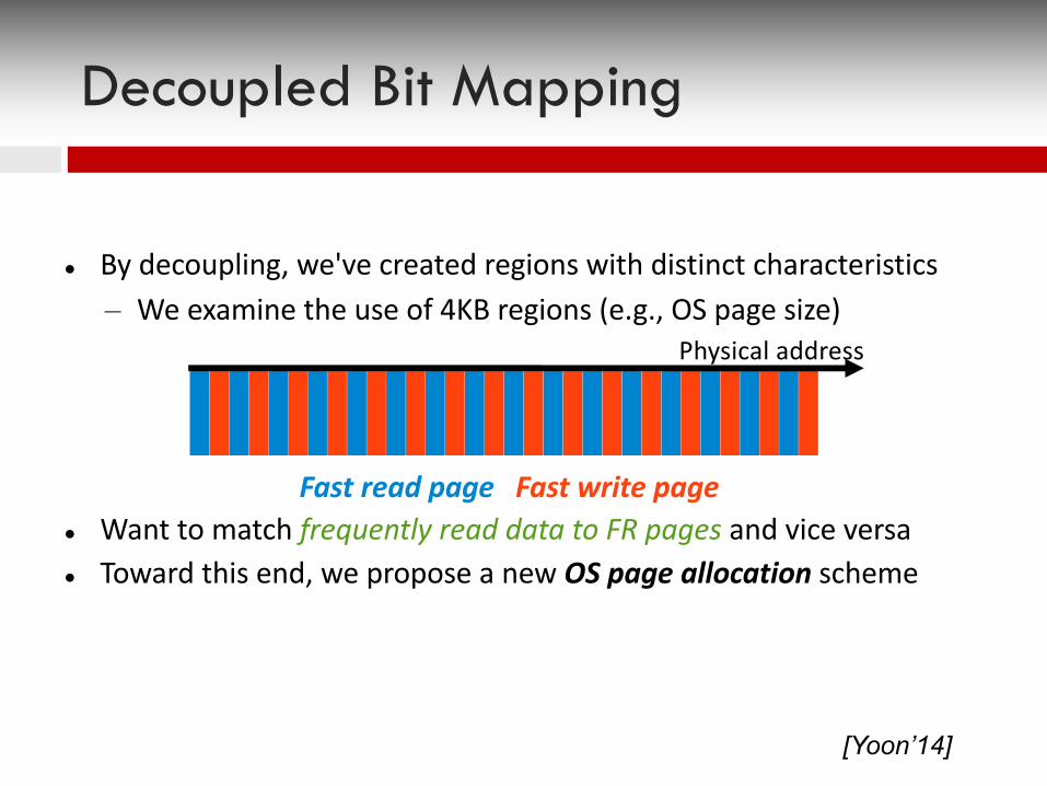
l By decoupling, we've created regions with distinct characteristics– We examine the use of 4KB regions (e.g., OS page size)
l Want to match frequently read data to FR pages and vice versal Toward this end, we propose a new OS page allocation scheme
Fast read page Fast write page
Physical address
Decoupled Bit Mapping
[Yoon’14]
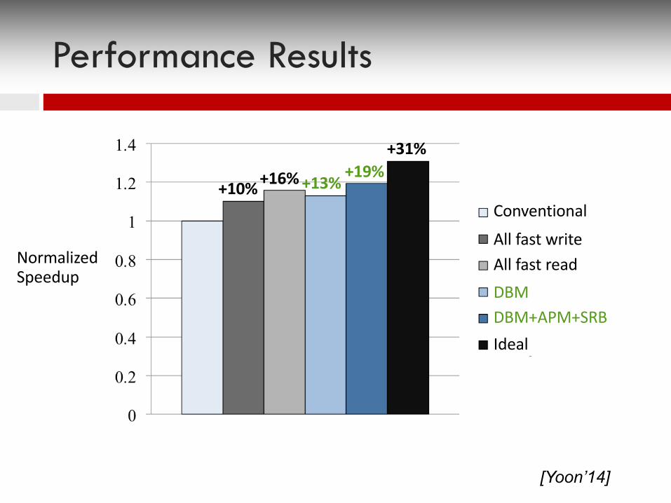
+19%+10%+16%+13%
+31%
Conventional
All fast writeAll fast readDBM DBM+APM+SRBIdeal
Normalized Speedup
Performance Results
[Yoon’14]


