43
Metamaterial Roadmap Metamorphose vision for the future advancements April 2008 Sergei Tretyakov, Ekmel Özbay, Christophe Crayene, and many other Metamorphose partners
Metamaterial Roadmap
Metamorphose vision for the future advancements
April 2008Sergei Tretyakov, Ekmel Özbay, Christophe
Crayene, and many other Metamorphose partners
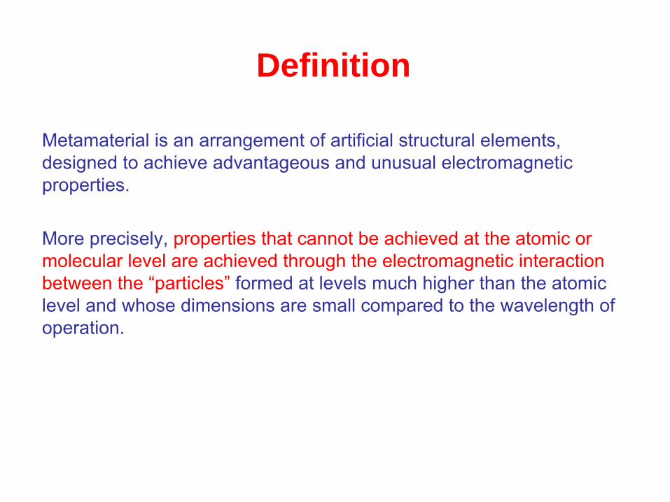
Metamaterial is an arrangement of artificial structural elements, designed to achieve advantageous and unusual electromagnetic properties.
More precisely,
properties that cannot be achieved at the atomic or molecular level are achieved through the electromagnetic interaction between the “particles”
formed at levels much higher than the atomic
level and whose dimensions are small compared to the wavelength of operation.
Definition

Metamaterials Research
Search in SCI for “metamaterials”Other common names, LHM, BW etc. not included

A Comparison of Metamaterials Research
Search in SCI for “metamaterials”Other common names, LHM, BW etc. not included

•
A European network of excellence (NoE) dedicated to metamaterials•
Coordinator: Prof. Sergei Tretyakov (TKK,
Finland)•
Strategic Manager: Dr. Vladimir Podlozny
(TKK, Finland)• Lifetime: June 2004 - May 2008• www.metamorphose-eu.org
METAMORPHOSE

1 Helsinki University
of Technology HUT Finland
2 Universite
Catholique de Louvain UCL Belgium
3 Universidad del País Vasco / Euskal
Herriko
Unibertsitatea UPV Spain
4 Swiss
Federal
Institute of Technology, Lausanne EPFL Switzerland
5 University
of Southampton UoS UK
6 Bilkent University Bilkent Turkey
7 Universidad
Publica
de Navarra UPNA Spain
8 University
of Glasgow U. Glasgow UK
9 Siegen University Siegen Germany
10 St. Petersburg Electrotechnical
University ETU Russia
11 FORTH, Institute of Electronic
Structure and Laser FORTH Greece
12 Warsaw
University WU Poland
13 University
Roma Tre Roma Tre Italy
14 Loughborough
University Lough UK
15 University
of Siena UNISI Italy
16 Thales Research
& Technology TRT France
17 Universitat
Politechnica
de Catalunya UPC Spain
18 Queen’s
University
of Belfast QUB UK
19 Université
Paris-Sud UPS/LEGEP France
20 Universidad
Autonoma
de Barcelona UAB Spain
21 Institute of Electronic
Materials
Technology ITME Poland
Participants

• Lifetime of Metamorphose: June 2004 - May 2008• New structure: Metamorphose VI•
One of the first virtual institutes envisioned by the EU
Commission to follow-up NoE• www.metamorphose-vi.org•
The Virtual Institute for Artificial Electromagnetic Materials
and Metamaterials (”Metamorphose VI”) is a non-for-profit international association whose purposes are the research, the study and the promotion of artificial electromagnetic materials and metamaterials• A research roadmap is one of the VI instruments
Life after METAMORPHOSE?

WIKIPEDIA
A roadmap may refer to:
A map of roads (where they might lead nobody knows), and possibly other features, to aid in navigation
A plan, e.g.
Road map for peace, to resolve the Israeli-Palestinian conflict
Technology roadmap, a management forecasting tool
What is a roadmap?
Goals
•
Get a clear idea of opportunities and challenges offered by metamaterials
•
Obtain a structured view of possible research orientations
•
Organise research at European level
o
to avoid overlaps
o
to achieve good coverage
o
to be fast picking up the fruits of joint efforts
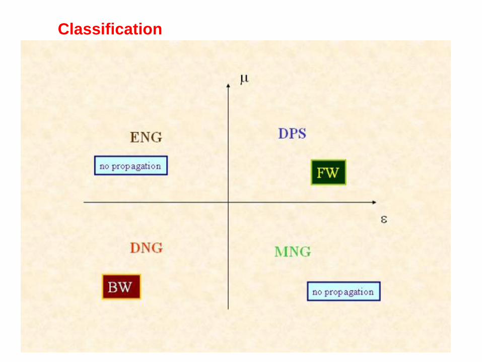
Classification
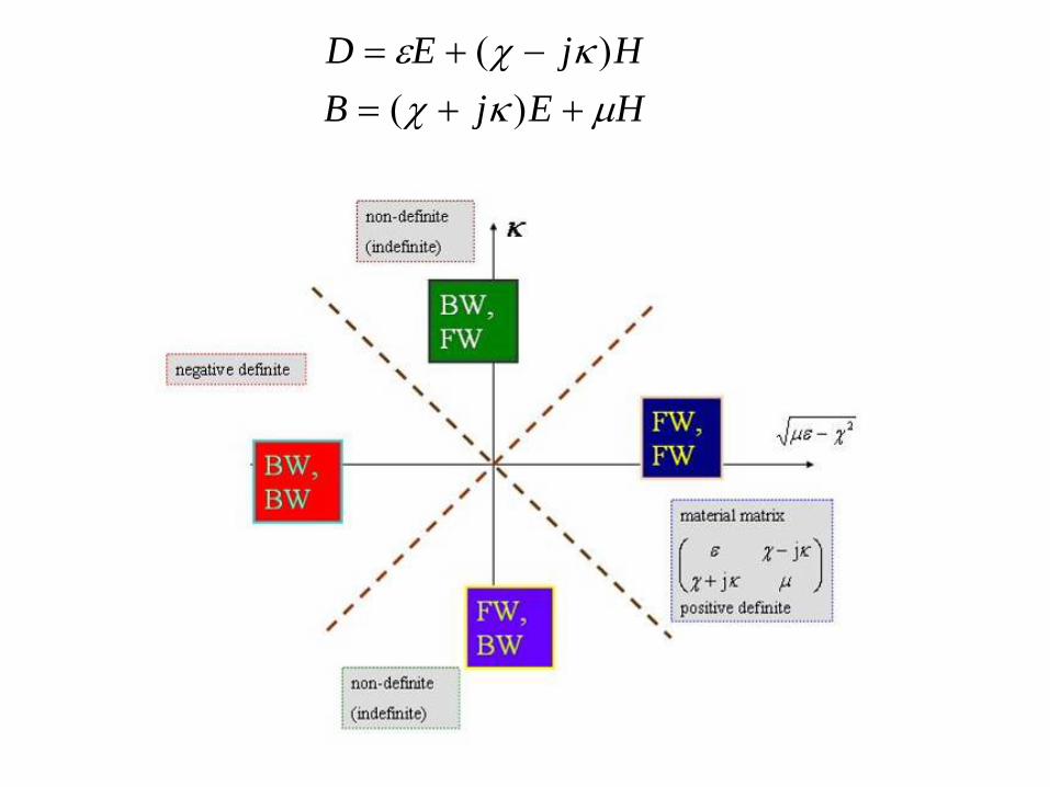
HEjBHjEDμκχ
κχε++=
−+=)(
)(


εμnη
ε μ n ηPEC perfect electric
conductorlarge small undefined very small
PMC perfect magnetic conductor
small large undefined very large
ZIM zero-index material small small very small undefined
IIM infinite-index material large large very large undefined
ZEM zero-electric material very small undefined small large
ZMM zero-magnetic material
undefined very small small small
IEM infinite-electric material
very large undefined large small
IMM infinite-magnetic material
undefined very large large large
Three wavelength regimes with different challenges:
1. Microwaves: based on well-established research in the field of antennas and microwave circuits.
2. TeraHertz: new field because of strong instrumental limitations at this stage.
3. Optics: also based on strong background, but bigger challenges, related to availability of low-loss nano-structured metamaterials and nano-fabrication techniques.
1.
Develop new processes and materials with engineered micro- or nano-scopic structure for improvement of microwave and millimetre-wave devices and creation of new devices with new capabilities, mainly for information technologies. The issues of
tunability, including electrical control, and integration in larger systems are at the forefront.
Different goals in different frequency ranges

2.
Create new artificial materials, devices and applications for TeraHertz frequencies, based on special phenomena, like left-
handed materials. The cost of fabrication and testing still being very high in this frequency range, the research roadmap in the field of TeraHertz
technologies will partly rely on conceptual
experiments at microwave frequencies.
Different goals in different frequency ranges
3. At optical frequencies, the first objective is to prove the feasibility of lensing
metamaterials with the help of artificial materials like
plasmonic devices, split-ring resonators and new types of materials and engineered (structural) thin sheets. Second, materials with extreme dielectric or magnetic properties are also looked for. A
big
challenge for material scientists is to find low-loss plasmonic materials.
Different goals in different frequency ranges
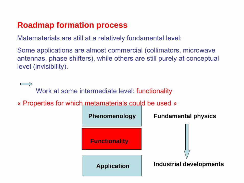
Roadmap formation processMatematerials
are still at a relatively fundamental level:
Some applications are almost commercial (collimators, microwave antennas, phase shifters), while others are still purely at conceptual level (invisibility).
Work at some intermediate level: functionality
«
Properties for which metamaterials
could be used
»
Functionality
Application
Phenomenology Fundamental physics
Industrial developments
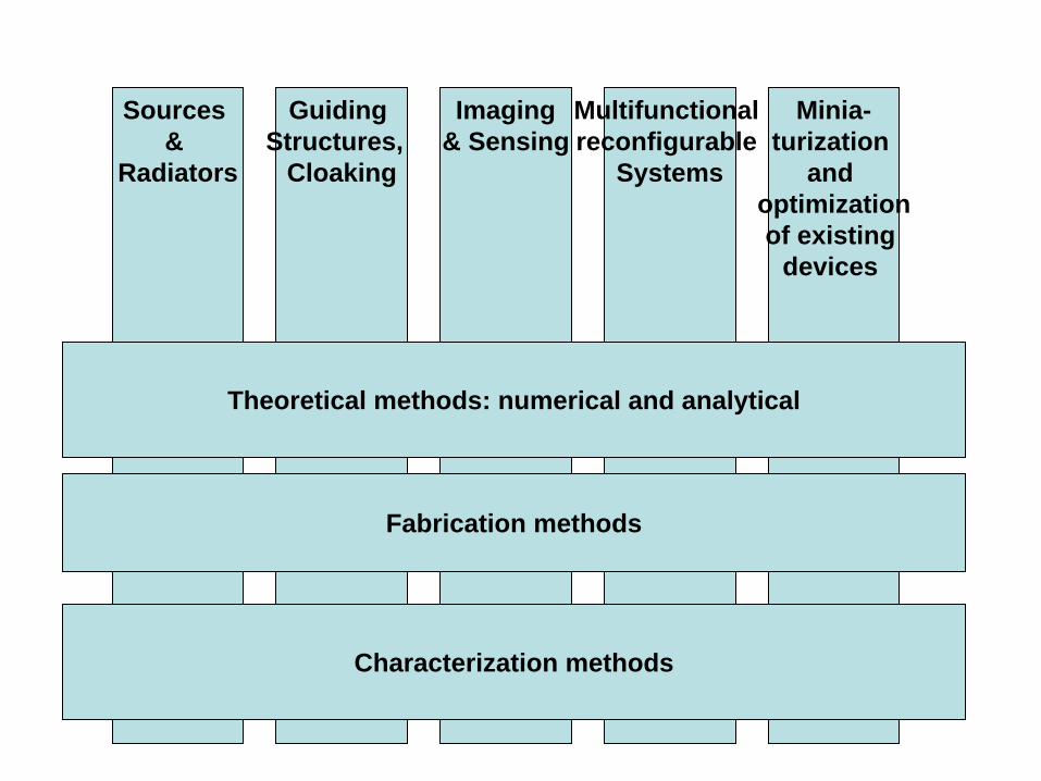
Minia- turization
and optimizationof existing
devices
Imaging& Sensing
Guiding Structures,
Cloaking
Sources &
Radiators
Multifunctional reconfigurable
Systems
Theoretical methods: numerical and analytical
Characterization methods
Fabrication methods
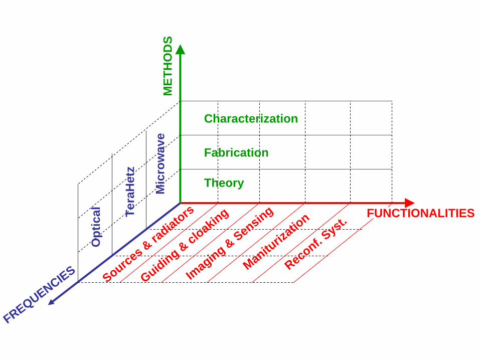
Tera
Het
z
Opt
ical
Mic
row
ave
Theory
Fabrication
Characterization
Guiding & cloaking
Sources & radiators
Manituriz
ation
Reconf. Syst.
Imaging & Sensing
FREQUENCIES
MET
HO
DS
FUNCTIONALITIES

Functionality Phenomenology Application (system)
Fabrication & measurement
Analysis techniques
Imaging and sensing
Collimation Low-epsilon materials, low-mu materials, spatial dispersion
MRI imaging, health applications,
Mechanical assembly
ASM, Method of Moments
lensing Matching + Refraction index close to -1, using DNG, SNG or chiral
material, plasmonic surfaces, strong spatial dispersion
Imaging, detection,focusing of power, health applications
Photo-
lithography, FTIR (Infrared and visible domain), 3D microwave imaging, micro and nano-
machining
Special treatment of resonant structures in Finite Element MethodEigenmode analysis
Sensing Resonance frequency shift
Biosensors nanolithography
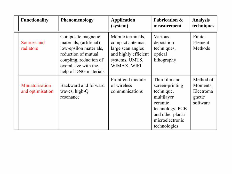
Sources and radiators
Composite magnetic materials, (artificial) low-epsilon materials, reduction of mutual coupling, reduction of overal
size with the help of DNG materials
Mobile terminals, compact antennas, large scan angles and highly efficient systems, UMTS, WIMAX, WIFI
Various deposition techniques, optical lithography
Finite Element Methods
Miniaturisation and optimisation
Backward and forward waves, high-Q resonance
Front-end module of wireless communications
Thin film and screen-printing technique, multilayer ceramic technology, PCB and other planar microelectronic technologies
Method of Moments, Electroma
gnetic software
Functionality Phenomenology Application (system)
Fabrication & measurement
Analysis techniques

Multi- functionnal reconfigu- rable systems
Reconfigurab-
ility/tunability
Dielectric response of ferro-electric material or varactors, tunable constitutive elements, ferroelectric varactors, non-
linear metamaterials, photonic FSS’s. Integration of MEMS switchesHBV
Reconfigurable components/fron
t-ends, electromagnetic windows, EM compatibility, tunable filters, parametric amplifiers, frequency multiplexers, mixers, Tunable
delay lines, phase shifters, tunable
filters
Photo and e-beam lithography, Thin film and screen-
printing technique, multilayer ceramic technology, PCB, RF-MEMS,Micro-milling, magnetron and laser sputtering, lithographye-beam lithography, nano-
imprintNano soft lithography, self assembly of nanostructures
Electromagne
tic software, and electrical solvers. Time-domain solvers for non-linear materials, Sonnet, Momentum, Harmonic balance simulations for large signal (non-
linear)
Functionality Phenomenolo gy
Application (system)
Fabrication & measurement
Analysis techniques

Expected achievements in 5 coming years:
Microwaves
3-D cloaking
devices

Expected achievements in 5 coming years:
TeraHertz
transparency
biosensing
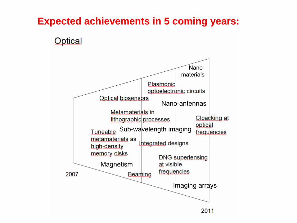
Expected achievements in 5 coming years:
Optics
Magnetism
Nano-antennas
Sub-wavelength
imaging
Imaging arrays
Nano-
materials

Conclusions and further prospects
•
Research topics (re)organized along 3 axes: functionalities, methods and frequencies
• Long-term expectations projected per frequency
• Contributions and cooperations determined
• Cooperation results will be reviewed every year
Yearly cycle within the Virtual Institute
• avoid
overlap
• get
coverage
•
reaping
fruits of efforts

New tunable metamaterial transmission lines based on CSRRs and varactors (UAB)

Metasurfaces for enhanced radiation properties (UPNa, LOUGH, TKK)

Metamorphose, NoE on Metamaterials http://www.metamorphose-eu.org/
Forth – UNISI - BilkentEfficient beaming at optical frequencies.

Broadband Broadband transpolarisingtranspolarising surfaces (UPC,UCL)surfaces (UPC,UCL)
Metamorphose, NoE on Metamaterials http://www.metamorphose-eu.org/
P.J. Ferrer
(UPC19), Carlos López-Martínez, X. Fàbregas, J.M. González-Arbesú
(UPC19), J. Romeu
(UPC19), A. Aguasca, and C. Craeye (UCL03),“Transpolarizing Surfaces for Polarimetric
SAR Systems Calibration”, IEEE Geoscience
and Remote Sensing (IGARSS07) conference.
P.J. Ferrer
(UPC19), J.M. González-Arbesú
(UPC19), J. Romeu
(UPC19), and C. Craeye (UCL03), “Design and Fabrication of a Cross-Polarising AMC Surface”, EuCAP07.
High Frequency and Quantum Electronics, University of Siegen
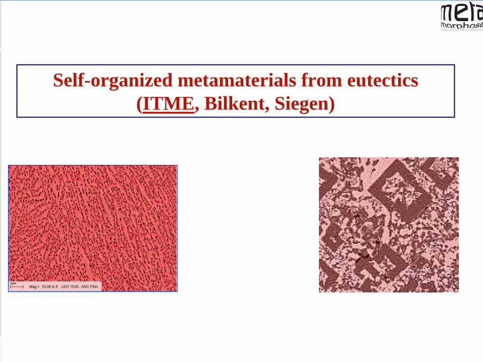
Self-organized metamaterials from eutectics (ITME, Bilkent, Siegen)
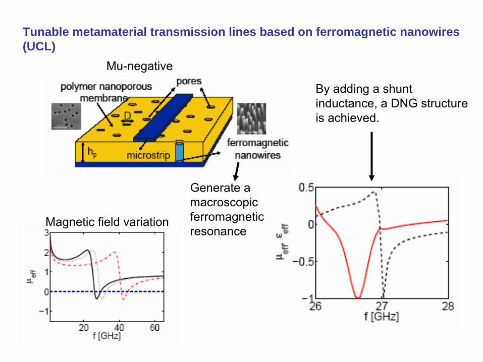
Tunable metamaterial transmission lines based on ferromagnetic nanowires (UCL)
Mu-negative
Generate
a macroscopic
ferromagnetic resonance
Magnetic
field
variation
By adding
a shunt inductance, a DNG structure
is
achieved.

Subwavelength resolution by a negative-index metamaterial superlens
OZBAY GROUP OZBAY GROUP -- BILKENT UNIVERSITY BILKENT UNIVERSITY Aydin et al., APL 90, 254102 (2007)
2D metamaterial composed of SRR and wire arrays
A left-handed transmission band is observed between 3.65 and 4.00 GHz.
At 3.74 GHz real part of ε
and μ
are equal, ε=μ=-1.8.
ε
and μ
are both negative btw. 3.63 and 3.93 GHz. Refractive index is also negative.
A point source is resolved by a 3-layer NIM superlens with a resolution of 0.13λ. The beam size in free space is on the order of wavelength. Two subwavelength features separated by distances of
λ/8, λ/5 and λ/3 are resolved with the superlens.

Tunable Dual-Band Microwave Filter Based on a Combination of Left/Right-Handed
Transmission Lines
Multilayer LTCC implementations of spurious-free stepped-impedance resonators and dual-band filters based on a combination of right-
and left-
handed transmission line (RH and LH TL) sections was derived. The measured microwave performance of the devices exhibited high resolution and excellent reproducibility. Based on the analysis of the tunability
of the devices based on RH and LH TLs
sections, the functionality of these miniature devices is further enhanced. The one-band tunable filter was designed using varactor
diodes.The combination of careful design of combined structures with a reliable three-dimensional low-cost fabrication technology opens a wide potential for commercial applications.
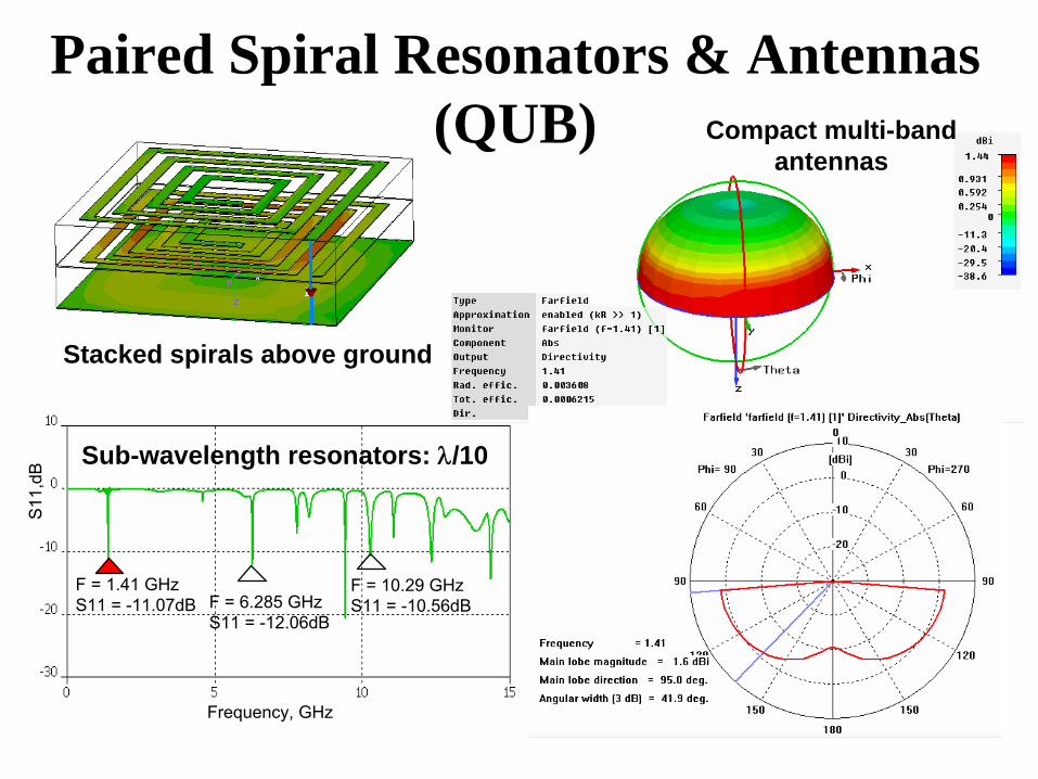
F = 1.41 GHzS11 = -11.07dB F = 6.285 GHz
S11 = -12.06dB
F = 10.29 GHzS11 = -10.56dB
Frequency, GHz
S11
,dB
Stacked spirals above ground
Sub-wavelength resonators: λ/10
Paired Spiral Resonators & Antennas (QUB) Compact multi-band
antennas

Tunable metamaterial-based stop-band filters in RF-MEMS technology
RF-MEMSCSRRMEASUREMENT (IL)
Actuation voltage: 17V

Meta-surfaces illuminated by dipole antennas
DipoleDipole + meta-
surface
Field confined on the aperture
•
Dipole antenna tuned to the pass band of the meta-surface
•
Thin profile = 0.137 λ0
at fr
=10.48 GHz•
Good matching S11
= -15 dB; •
Enhanced directivity D = 8.2 dBi
•
High aperture efficiency: ηap
= 1.1 •
High radiation efficiency ηr:
ηr dipole
= 0.98; ηr
superstrate
=0.90•
Low back radiation
•
Mutual coupling reduction in array configuration
In collaboration with Bilkent
University and Helsinki
University of Technology
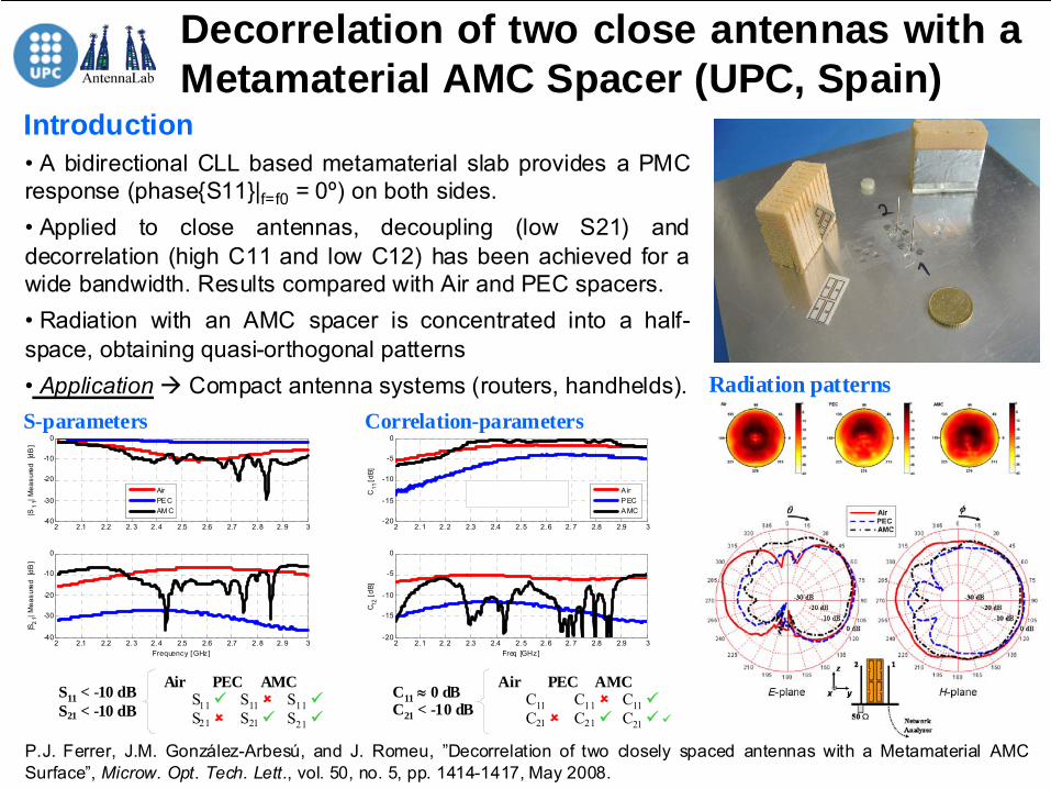
Decorrelation of two close antennas with a Metamaterial AMC Spacer (UPC, Spain)
Introduction
Radiation patterns
P.J. Ferrer, J.M. González-Arbesú, and J. Romeu, ”Decorrelation of two closely spaced antennas with a Metamaterial AMC Surface”, Microw. Opt. Tech. Lett., vol. 50, no. 5, pp. 1414-1417, May 2008.
2 2.1 2.2 2.3 2.4 2.5 2.6 2.7 2.8 2.9 3-40
-30
-20
-10
0
|S1
1| Mea
sure
d [d
B]
AirPE CAM C
2 2.1 2.2 2.3 2.4 2.5 2.6 2.7 2.8 2.9 3-40
-30
-20
-10
0
Frequency [GHz]
|S2
1| Mea
sure
d [d
B]
S-parameters
S11 < -10 dBS21 < -10 dB
AirS11S21
PECS11S21
AMCS11S21
2 2.1 2.2 2.3 2.4 2.5 2.6 2.7 2.8 2.9 3-20
-15
-10
-5
0
C11
[dB]
A irP ECA MC
2 2.1 2.2 2.3 2.4 2.5 2.6 2.7 2.8 2.9 3-20
-15
-10
-5
0
C 12 [d
B]
Freq [GHz]
Correlation-parameters
C11 ≈ 0 dBC21 < -10 dB
AirC11C21
PECC11C21
AMCC11C21
• A bidirectional CLL based metamaterial slab provides a PMC response (phase{S11}|f=f0 = 0º) on both sides.• Applied to close antennas, decoupling (low S21) and decorrelation (high C11 and low C12) has been achieved for a wide bandwidth. Results compared with Air and PEC spacers.• Radiation with an AMC spacer is concentrated into a half-space, obtaining quasi-orthogonal patterns• Application Compact antenna systems (routers, handhelds).

Electromagnetic cloaking based on transmission-line networks (TKK)
Total SCS is shown to be greatly reduced in a large bandwidth Electric field at 2 GHz:
Transmission-line networks designed for the reduction of the total scattering cross section of periodic structures (2D arrays of metal rods here)
1.5 1.75 2 2.25 2.50
0.5
1
1.5
f [GHz]
SC
S r
ati
o
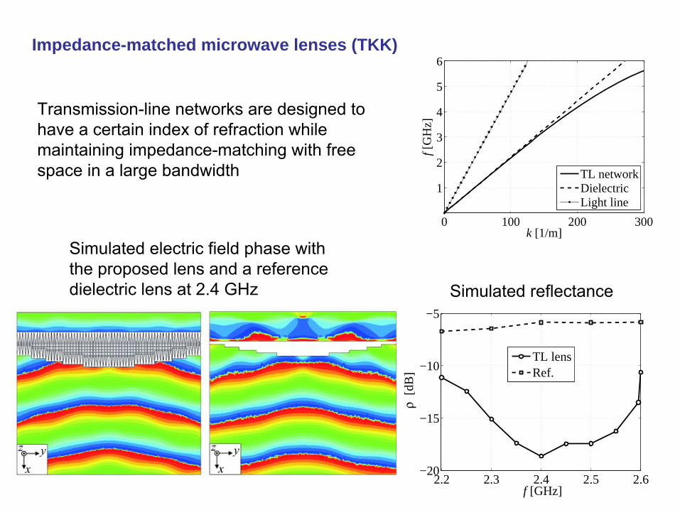
Impedance-matched microwave lenses (TKK)
Simulated electric field phase with the proposed lens and a reference dielectric lens at 2.4 GHz Simulated reflectance
Transmission-line networks are designed to have a certain index of refraction while maintaining impedance-matching with free space in a large bandwidth
0 100 200 300
1
2
3
4
5
6
k [1/m]
f [G
Hz]
TL networkDielectricLight line
2.2 2.3 2.4 2.5 2.6−20
−15
−10
−5
f [GHz]
ρ [
dB]
TL lensRef.

Cooperation
NMP ThemeCall identifier: FP7-NMP-2007-CSA-1
COORDINATING AND SUPPORT ACTION (Coordinating)
Project acronym:
ECONAMProject full title:
Electromagnetic Characterization of Nanostructured Materials
Work programme topics addressed: NMP-2007-2.1-3 Characterisation of nanostructured materials

THANK YOU!
Dziękuję!Dank
u!
Merci!
Gracias!
Danke
schön!
GRAZIE!
Спасибo!
Kiitos!
Tag!
ευχαριστώ
πολύ!
TEŞEKKÜR!


![Lifting Layers: Analysis and ApplicationsLifting Layers: Analysis and Applications Peter Ochs* y, Tim Meinhardt z, Laura Leal-Taixe , Michael Moeller*],]University of Siegen, Siegen,](https://static.documents.pub/doc/80x56/5e923212b554e03ca7720a09/lifting-layers-analysis-and-applications-lifting-layers-analysis-and-applications.jpg)


