110
Results of Bare Die Probing for RF Booster Chip at 450, 915, and 2400 MHz by Gregory Mitchell and John Penn ARL-TR-5170 April 2010 Approved for public release; distribution unlimited.
Results of Bare Die Probing for RF Booster Chip
at 450, 915, and 2400 MHz
by Gregory Mitchell and John Penn
ARL-TR-5170 April 2010 Approved for public release; distribution unlimited.

NOTICES
Disclaimers The findings in this report are not to be construed as an official Department of the Army position unless so designated by other authorized documents. Citation of manufacturer’s or trade names does not constitute an official endorsement or approval of the use thereof. Destroy this report when it is no longer needed. Do not return it to the originator.

Army Research Laboratory Adelphi, MD 20783-1197
ARL-TR-5170 April 2010
Results of Bare Die Probing for RF Booster Chip at 450, 915, and 2400 MHz
Gregory Mitchell and John Penn
Sensors and Electron Devices Directorate, ARL Approved for public release; distribution unlimited.

ii
REPORT DOCUMENTATION PAGE Form Approved OMB No. 0704-0188
Public reporting burden for this collection of information is estimated to average 1 hour per response, including the time for reviewing instructions, searching existing data sources, gathering and maintaining the data needed, and completing and reviewing the collection information. Send comments regarding this burden estimate or any other aspect of this collection of information, including suggestions for reducing the burden, to Department of Defense, Washington Headquarters Services, Directorate for Information Operations and Reports (0704-0188), 1215 Jefferson Davis Highway, Suite 1204, Arlington, VA 22202-4302. Respondents should be aware that notwithstanding any other provision of law, no person shall be subject to any penalty for failing to comply with a collection of information if it does not display a currently valid OMB control number. PLEASE DO NOT RETURN YOUR FORM TO THE ABOVE ADDRESS.
1. REPORT DATE (DD-MM-YYYY)
April 2010 2. REPORT TYPE
Summary 3. DATES COVERED (From - To)
FY009 4. TITLE AND SUBTITLE
Results of Bare Die Probing for RF Booster Chip at 450, 915, and 2400 MHz 5a. CONTRACT NUMBER
5b. GRANT NUMBER
5c. PROGRAM ELEMENT NUMBER
6. AUTHOR(S)
Gregory Mitchell and John Penn 5d. PROJECT NUMBER
5e. TASK NUMBER
5f. WORK UNIT NUMBER
7. PERFORMING ORGANIZATION NAME(S) AND ADDRESS(ES)
U.S. Army Research Laboratory ATTN: RDRL-SER-E 2800 Powder Mill Road Adelphi, MD 20783-1197
8. PERFORMING ORGANIZATION REPORT NUMBER
ARL-TR-5170
9. SPONSORING/MONITORING AGENCY NAME(S) AND ADDRESS(ES)
10. SPONSOR/MONITOR’S ACRONYM(S) 11. SPONSOR/MONITOR'S REPORT NUMBER(S)
12. DISTRIBUTION/AVAILABILITY STATEMENT
Approved for public release; distribution unlimited.
13. SUPPLEMENTARY NOTES
14. ABSTRACT
Low-power radio frequency (RF) transceivers have been used for low-cost, high volume commercial applications that do not always meet the needs of critical Army systems. In low-power applications, a tradeoff between transmit range and battery life exists. A simple means of extending transmit range would be to add a custom integrated circuit (IC) between the transceiver and antenna. Using appropriate technologies, a tradeoff in size, efficiency, and performance is achievable. We present a custom design using gallium arsenide (GaAs) technology to provide enhanced performance. This design optimizes the output power, noise figure, power added efficiency, insertion loss, and range performance of an overall low-power RF system.
15. SUBJECT TERMS
RF front end enhancement, gallium arsenide, MMIC, RFIC
16. SECURITY CLASSIFICATION OF: 17. LIMITATION OF ABSTRACT
UU
18. NUMBER OF PAGES
110
19a. NAME OF RESPONSIBLE PERSON Gregory Mitchell
a. REPORT
Unclassified b. ABSTRACT
Unclassified c. THIS PAGE
Unclassified 19b. TELEPHONE NUMBER (Include area code) (301) 394-3233
Standard Form 298 (Rev. 8/98) Prescribed by ANSI Std. Z39.18

iii
Contents
List of Figures v
List of Tables xi
1. Introduction 1
2. Description of RFIC Booster Chip 1
3. Experimental Results of RFIC Booster Chip Designs 2
3.1 ARL01M900 – Cascaded Narrowband BPSK Modulator and PA Design at 900 MHz ..........................................................................................................................2
3.2 ARL02M450 – Cascaded Narrowband BPSK Modulator and PA Design at 450 MHz ..........................................................................................................................8
3.3 ARL03M900 – Narrowband BPSK Modulator, PA, Narrowband LNA, and TR Switch at 900 MHz ........................................................................................................13
3.4 ARL04M900 – Broadband BPSK Modulator, PA, LNA, and TR Switch at 900 MHz ........................................................................................................................20
3.5 ARL05M450 – BPSK Modulator, PA, Narrowband LNA, and TR Switch at 450 MHz ........................................................................................................................25
3.6 ARL06M450 – BPSK Modulator, PA, Narrowband LNA, TR Switch with Additional PA and LNA Enable Inputs at 450 MHz .......................................................................31
3.7 ARL07G24 – BPSK Modulator, PA, Narrowband LNA, and TR Switch at 2.4 GHz .37
3.8 ARL08M450 – Cascaded BPSK Modulator and PA Redesign with Current Mirror at 450 MHz ........................................................................................................................41
3.9 ARL09G24 – BPSK Modulator, PA, Narrowband LNA, and TR Switch Redesign with Current Mirror at 2.4 GHz .............................................................................................49
3.10 ARL10M900 – BPSK Modulator, PA, Narrowband LNA, and TR Switch Redesign at 900 MHz ........................................................................................................................58
3.11 ARL11M450 – BPSK Modulator, PA, Narrowband LNA, TR Switch with Additional PA, and LNA Enable Input Redesign at 450 MHz .......................................................63
3.12 ARL12M450 – BPSK Modulator, PA, and TR Switch Design at 450 MHz ................70
3.13 ARL13M450 – Individual BPSK Modulator and PA Redesign without Current Mirror at 450 MHz ....................................................................................................................73

iv
3.14 ARL14G24 – BPSK Modulator, PA, Narrowband LNA, and TR Switch Redesign with Current Mirror at 2.4 GHz .............................................................................................82
4. Performance Summary 90
5. Conclusions 92
6. Path Forward 92
List of Symbols, Abbreviations, and Acronyms 94
Distribution List 95

v
List of Figures
Figure 1. Layout for cascaded BPSK modulator and PA at 900 MHz. ..........................................2
Figure 2. Measured versus simulated S-parameters for cascaded BPSK modulator and PA for 2.7-V DC in state A at 900 MHz. Dashed lines are simulated and solid lines are measured data points. .................................................................................................................3
Figure 3. Measured versus simulated S-parameters for cascaded BPSK modulator and PA for 2.7-V DC in state B at 900 MHz. Dashed lines are simulated and solid lines are measured data points. ................................................................................................................4
Figure 4. Measured versus simulated phase of cascaded BPSK modulator and PA for 2.7 V in at 900 MHz. Pink is simulated and blue is measured data points. ........................................5
Figure 5. Measured gain, PAE, and output power versus input power for cascaded BPSK modulator and PA for 2.7 and 3.0 V at 900 MHz. .....................................................................6
Figure 6. The broadband behavior of the LNA gain and NF from 0.6–1.6 GHz. ..........................7
Figure 7. Layout for narrowband cascaded BPSK modulator and PA at 450 MHz. ......................8
Figure 8. Measured versus simulated S-parameters for cascaded BPSK modulator and PA for 3.0 V DC in state A at 450 MHz. Dashed lines are simulated and solid lines are measured data points. .................................................................................................................9
Figure 9. Measured versus simulated S-parameters for cascaded BPSK modulator and PA for 3.0 V DC in state B at 450 MHz. Dashed lines are simulated and solid lines are measured data points. ...............................................................................................................10
Figure 10. Measured versus simulated phase of cascaded BPSK modulator and PA for 3.0 V in at 450 MHz. Pink is measured and blue is simulated data points. ......................................11
Figure 11. Measured gain, PAE, and output power versus input power for cascaded BPSK modulator for 3.0 V at 450 MHz. ...........................................................................................12
Figure 12. Layout for 1.66x2.41 mm narrowband RFIC design at 900 MHz. .............................14
Figure 13. Measured versus simulated S-parameters of the RFIC transmit stage for 3.0 V DC in state A at 900 MHz. Dashed lines are simulated and solid lines are measured data points. .......................................................................................................................................15
Figure 14. Measured versus simulated S-parameters of the RFIC transmit stage for 3.0 V DC in state B at 900 MHz. Dashed lines are simulated and solid lines are measured data points. .......................................................................................................................................15
Figure 15. Measured versus simulated phase difference of the RFIC transmit stage for 3.0 V DC in at 900 MHz. Pink is measured and blue is simulated data points. ...............................16
Figure 16. Comparison between phase data of chip ARL03M900 and ARL01M900 at 900 MHz. Green is results of the full RFIC chip and blue is for the transmit stage without the TR switch. ............................................................................................................17
Figure 17. Measured gain, PAE, and output power versus input power for cascaded BPSK modulator, PA, and TR switch for 3.0-V input power at 450 MHz. ......................................18

vi
Figure 18. Comparisons between measured and simulated data for the LNA in absence of the TR switch. ................................................................................................................................19
Figure 19. Layout for 1.66x1.52 mm RFIC design at 900 MHz. .................................................20
Figure 20. Measured versus simulated S-parameters for cascaded BPSK modulator and PA for 3.0 V DC state A at 900 MHz. Dashed lines are simulated and solid lines are measured data points. ...............................................................................................................21
Figure 21. Measured versus simulated S-parameters for cascaded BPSK modulator and PA for 3.0 V DC state B at 900 MHz. Dashed lines are simulated and solid lines are measured data points. ...............................................................................................................21
Figure 22. Measured versus simulated phase difference of the RFIC transmit stage for 3.0 V DC at 900 MHz. Pink is measured and blue is simulated data points. ..................................22
Figure 23. Measured gain, PAE, and output power versus input power for cascaded BPSK modulator, PA, and TR switch for 3.0 V input power at 400, 450, and 600 MHz. .................23
Figure 24. S-parameters for a broadband LNA design from 450 MHz to 1.2 GHz with acceptable NF and gain data. ..................................................................................................24
Figure 25. The broadband behavior of the gain and NF from 0.2–3.0 GHz. ................................25
Figure 26. Layout for 1.66 mm x 2.41 mm RFIC booster design at 450 MHz. ..........................26
Figure 27. Measured versus simulated S-parameters for cascaded BPSK modulator and PA for 3.0 V DC state B at 450 MHz. Dashed lines are simulated and solid lines are measured data points. ...............................................................................................................27
Figure 28. Measured versus simulated S-parameters of the cascaded TR switch and LNA at 3.0 V DC state B at 450 MHz in the OFF state. Dashed lines are simulated and solid lines are measured data points. ................................................................................................27
Figure 29. Measured versus re-simulated S-parameters of cascaded TR switch and LNA including the actual shorted connection at 3.0 V. Dashed lines are simulated and solid lines are measured data points. ................................................................................................28
Figure 30. Shows a short in the circuit which causes the gain problems of the PA in the transmit stage of the measured data. ........................................................................................28
Figure 31. Measured versus simulated phase difference of the RFIC transmit stage for 3.0 V DC at 450 MHz. Pink is measured and blue is simulated data points. ...................................29
Figure 32. Measured gain, PAE, and output power versus input power for cascaded BPSK modulator, PA, and TR switch for 3.0 V input power at 400, 450, and 600 MHz. ................30
Figure 33. Layout for 1.66x2.41 mm RFIC booster design with PA and LNA gate enable at 450 MHz. .................................................................................................................................32
Figure 34. Measured versus simulated S-parameters for cascaded BPSK modulator and PA for modulation state A at 450 MHz. Dashed lines are simulated and solid lines are measured data points. ...............................................................................................................33
Figure 35. Measured versus simulated S-parameters for cascaded BPSK modulator and PA for modulation state B at 450 MHz. Dashed lines are simulated and solid lines are measured data points. ...............................................................................................................33

vii
Figure 36. Measured versus simulated phase difference of the RFIC transmit stage for 3.0 V DC at 450 MHz. Pink is measured and blue is simulated data points. ..................................34
Figure 37. Measured versus simulated S-parameters for a LNA design at 450 MHz. Dashed lines are simulated and solid lines are measured data points. ..................................................35
Figure 38. The behavior of the gain and NF for the LNA at 450 MHz. .......................................35
Figure 39. Measured gain, PAE, and output power versus input power for cascaded BPSK modulator, PA, and TR switch for 3.0 V input power at 400, 450, and 600 MHz. ................36
Figure 40. Layout for 1.66 mm x 1.52 mm RFIC booster design at 2.4 GHz. .............................38
Figure 41. Measured versus simulated S-parameters for cascaded BPSK modulator and PA for modulation state A at 2.4 GHz. Dashed lines are simulated and solid lines are measured data points. ...............................................................................................................39
Figure 42. Measured versus simulated S-parameters for cascaded BPSK modulator and PA for modulation state B at 2.4 GHz. Dashed lines are simulated and solid lines are measured data points. ...............................................................................................................39
Figure 43. Measured versus simulated phase difference of the RFIC transmit stage for 3.0 V DC at 2.4 GHz. Blue is measured and brown is simulated data points. ................................40
Figure 44. Measured versus simulated S-parameters for a LNA design at 2.4 GHz. Dashed lines are simulated and solid lines are measured data points. ..................................................41
Figure 45. Layout for narrowband cascaded BPSK modulator and PA redesign with robust current mirror at 450 MHz. ......................................................................................................42
Figure 46. Measured versus simulated S-parameters for cascaded BPSK modulator and PA redesign with robust current mirror for modulation state A at 450 MHz. Dashed lines are simulated and solid lines are measured data points. ................................................................43
Figure 47. Measured versus simulated S-parameters for cascaded BPSK modulator and PA redesign with robust current mirror for modulation state B at 2.4 GHz. Dashed lines are simulated and solid lines are measured data points. ................................................................43
Figure 48. Measured versus simulated phase difference of the transmit stage redesign with robust current mirror for 3.0 V DC at 450 MHz. Blue is measured and pink is simulated data points. ...............................................................................................................................44
Figure 49. Measured PAE versus input power for cascaded BPSK modulator and PA redesign with bust current mirror for 2.0 to 5.0 V DC at 450 MHz. ......................................45
Figure 50. Measured output power versus input power for cascaded BPSK modulator and PA redesign with robust current mirror for 2.0 to 5.0 V DC at 450 MHz. ..............................46
Figure 51. Layout for 1.66x1.52 mm RFIC booster redesign with robust current mirror at 2.4 GHz. ...................................................................................................................................49
Figure 52. Measured versus simulated S-parameters for transmit stage with robust current mirror for modulation state A at 2.4 GHz. Dashed lines are simulated and solid lines are measured data points. ...............................................................................................................50
Figure 53. Measured versus simulated S-parameters for transmit stage with robust current mirror for modulation state B at 2.4 GHz. Dashed lines are simulated and solid lines are measured data points. ...............................................................................................................50

viii
Figure 54. Measured gain of ARL07G24 versus ARL09G24 for both modulation states of the transmit stage at 2.4 GHz. ..................................................................................................51
Figure 55. Measured input match of ARL07G24 versus ARL09G24 for both modulation states of the transmit stage at 2.4 GHz. ....................................................................................52
Figure 56. Measured output match of ARL07G24 versus ARL09G24 for both modulation states of the transmit stage at 2.4 GHz. ....................................................................................53
Figure 57. Measured versus simulated S-parameters for receive stage at 2.4 GHz. Dashed lines are simulated and solid lines are measured data points. ..................................................54
Figure 58. Measured versus simulated phase difference of the transmit stage redesign with robust current mirror for 3.0 V DC at 2.4 GHz. Blue is measured and brown is simulated data points. ...............................................................................................................................55
Figure 59. Measured PAE, output power, and gain versus input power for cascaded BPSK modulator and PA redesign with robust current mirror at 2.7 and 3.3 V DC at 2.4 GHz. ......56
Figure 60. Layout for 1.66x2.41 mm narrowband RFIC booster redesign at 900 MHz. ............58
Figure 61. Measured versus simulated S-parameters for transmit stage with robust current mirror for modulation state A at 900 MHz. Dashed lines are simulated and solid lines are measured data points. ...............................................................................................................59
Figure 62. Measured versus simulated S-parameters for transmit stage with robust current mirror for modulation state B at 900 MHz. Dashed lines are simulated and solid lines are measured data points. ..............................................................................................................59
Figure 63. Measured versus simulated phase difference of the transmit stage redesign with robust current mirror at 900 MHz. Blue is measured and pink is simulated data points. ......60
Figure 64. Measured versus simulated S-parameters for receive stage at 900 MHz. Dashed lines are simulated and solid lines are measured data points. ..................................................61
Figure 65. The behavior of the gain and NF for the LNA at 900 MHz. .......................................61
Figure 66. Measured PAE, output power, and gain versus input power for cascaded BPSK modulator and PA redesign with robust current mirror for 2.7 V at 900 MHz. ......................62
Figure 67. Layout for 1.66x2.41 mm RFIC booster redesign design at 450 MHz. ......................64
Figure 68. Measured versus simulated S-parameters for transmit stage for modulation state A at 450 MHz. Solid traces are the measured data points and dotted traces are the simulated values. ......................................................................................................................65
Figure 69. Measured versus simulated S-parameters for transmit stage for modulation state B at 450 MHz. Solid traces are the measured data points and dotted traces are the simulated values. ......................................................................................................................65
Figure 70. Measured versus simulated phase difference of the transmit at 450 MHz. Blue is measured and pink is simulated data points. ............................................................................66
Figure 71. Measured versus simulated S-parameters for receive stage at 450 MHz. Solid traces are the measured data points and dotted traces are the simulated values. .....................67
Figure 72. Measured versus simulated S-parameters for receive stage at 450 MHz with TR switch set to transmit. Solid traces are the measured data points and dotted traces are the simulated values. ......................................................................................................................67

ix
Figure 73. The behavior of the gain and NF for the LNA at 450 MHz. .......................................68
Figure 74. Measured PAE, output power, and gain versus input power for cascaded BPSK modulator and PA redesign with robust current mirror for 2.7 V at 900 MHz. ......................69
Figure 75. Layout for cascaded BPSK modulator, PA, and TR switch at 450 MHz. ...................71
Figure 76. Measured versus simulated S-parameters for transmit stage for modulation state A at 450 MHz. Dashed lines are simulated and solid lines are measured data points. ..........71
Figure 77. Measured versus simulated S-parameters for transmit stage for modulation state B at 450 MHz. Dashed lines are simulated and solid lines are measured data points. ..........72
Figure 78. Measured versus simulated phase difference of the transmit stage redesign with robust current mirror at 900 MHz. Blue is measured and pink is simulated data points. ......73
Figure 79. Layout of cascaded BPSK modulator and PA design with additional GSC pads at 450 MHz. .................................................................................................................................74
Figure 80. Measured versus simulated gain for PA at 450 MHz. The red traces are measured data points at 2.7 V, while the other traces are simulations at 2.5 and 3.0 V. ........75
Figure 81. Measured versus simulated input match for PA at 450 MHz. Red is the measured data points. ...............................................................................................................75
Figure 82. Measured versus simulated output match for PA at 450 MHz. The red line is measured data...........................................................................................................................76
Figure 83. Measured input match for BPSK modulator in modulation state A from 1.8 to 5.0 V DC input at 450 MHz. ....................................................................................................77
Figure 84. Measured input match for BPSK modulator in modulation state B from 1.8 to 5.0 V DC input at 450 MHz. ....................................................................................................77
Figure 85. Measured insertion loss for BPSK modulator in modulation state A from 1.8 to 5.0 V DC input at 450 MHz. ....................................................................................................78
Figure 86. Measured insertion loss for BPSK modulator in modulation state B from 1.8 to 5.0 V DC input at 450 MHz. ....................................................................................................79
Figure 87. Measured versus simulated phase difference of the transmit stage redesign with robust current mirror at 2.4 GHz. Green is measured and purple is simulated data points. ...80
Figure 88. Measured PAE, output power, and gain versus input power for PA for 2.7 V at 450 MHz. .................................................................................................................................81
Figure 89. Layout of 1.66x1.52 mm RFIC design with additional GSC pads at 2.4 GHz. ..........83
Figure 90. Measured versus simulated gain for PA at 2.4 GHz. The blue and red traces are measured data...........................................................................................................................83
Figure 91. Measured versus simulated input match for PA at 2.4 GHz. The red trace is the measured data...........................................................................................................................84
Figure 92. Measured versus simulated output match for PA at 2.4 GHz. The red trace is the measured data...........................................................................................................................85
Figure 93. Measured S-parameters for BPSK modulator in both modulation states at 450 MHz. .................................................................................................................................86

x
Figure 94. Measured versus simulated phase difference of the transmit stage redesign with robust current mirror at 2.4 GHz. Green is measured and purple is simulated data points. ..87
Figure 95. Measured versus re-simulated s-parameters for the LNA with an error in the input match layout at 2.4 GHz. The solid traces are measured data and the dotted traces are simulations. ........................................................................................................................88
Figure 96. Measured PAE, output power, and gain versus input power for cascaded BPSK modulator and PA redesign with robust current mirror for 2.7 V at 900 MHz. ......................89

xi
List of Tables
Table 1. Measured gain, PAE, and output power versus input power for cascaded BPSK modulator and PA for 2.7 V at 900 MHz...................................................................................6
Table 2. Measured gain, PAE, and output power versus input power for cascaded BPSK modulator and PA for 3.0 V at 900 MHz...................................................................................7
Table 3. Measured gain, PAE, and output power versus input power for cascaded BPSK modulator and PA for 3.0 V at 900 MHz................................................................................12
Table 4. Measured gain, PAE, and output power versus input power for cascaded BPSK modulator PA, and TR switch for a 2.7-V DC input at 16 mA at 450 MHz. ..........................18
Table 5. Measured gain, PAE, and output power versus input power for cascaded BPSK modulator PA, and TR switch for 3.0 V DC and 27 mA input at 900 MHz. ..........................19
Table 6. Measured gain, PAE, and output power versus input power for cascaded BPSK modulator PA, and TR switch for 3.0 V at 600 MHz. .............................................................23
Table 7. Measured gain, PAE, and output power versus input power for cascaded BPSK modulator PA, and TR switch for 3.0 V at 450 MHz. .............................................................30
Table 8. Measured gain, PAE, and output power versus input power for cascaded BPSK modulator PA, and TR switch for 3.0 V at 450 MHz. .............................................................37
Table 9. Measured gain, PAE, and output power versus input power for cascaded BPSK modulator and PA or 2.0 V at 450 MHz. .................................................................................47
Table 10. Measured gain, PAE, and output power versus input power for cascaded BPSK modulator and PA for 3.0 V at 450 MHz.................................................................................47
Table 11. Measured gain, PAE, and output power versus input power for cascaded BPSK modulator and PA for 4.0 V at 450 MHz.................................................................................48
Table 12. Measured gain, PAE, and output power versus input power for cascaded BPSK modulator and PA for 5.0 V at 450 MHz.................................................................................48
Table 13. Measured gain, PAE, and output power versus input power for cascaded BPSK modulator PA, and TR switch for 2.7 V at 2.4 GHz. ...............................................................57
Table 14. Measured gain, PAE, and output power versus input power for cascaded BPSK modulator PA, and TR switch for 3.3 V at 2.4 GHz. ...............................................................57
Table 15. Measured gain, PAE, and output power versus input power for cascaded BPSK modulator PA, and TR switch for 2.7 V at 2.4 GHz. ...............................................................63
Table 16. Measured gain, PAE, and output power versus input power for cascaded BPSK modulator PA, and TR switch for 2.7 V at 450 MHz. .............................................................69
Table 17. Measured gain, PAE, and output power versus input power for cascaded BPSK modulator PA, and TR switch for 3.0 V at 450 MHz. .............................................................70
Table 18. Measured gain, PAE, and output power versus input power for PA at 2.7 V and 2.4 GHz. ...................................................................................................................................82

xii
Table 19. Measured gain, PAE, and output power versus input power for PA at 3.0 V and 2.4 GHz. ...................................................................................................................................82
Table 20. Measured gain, PAE, and output power versus input power for PA at 2.7 V and 2.4 GHz. ...................................................................................................................................90
Table 21. Measured gain, PAE, and output power versus input power for PA at 3.0 V and 2.4 GHz. ...................................................................................................................................90
Table 22. A summary of the performance of the various designs. ................................................91

1
1. Introduction
This report documents the results of laboratory testing of the bare die of 14 radio frequency (RF) integrated circuit (RFIC) chips designed to enhance the performance of the front end of a low-power RF identification (RFID) tag. The designs and all simulation results presented in this report were documented in a previous report1
2. Description of RFIC Booster Chip
. The first pass of these designs were done on gallium arsenide (GaAs) with the intention of transitioning them to silicon germanium (SiGe) for use in software controlled radio architectures. The GaAs results should provide a benchmark for comparison to future SiGe designs, and also allow the design engineers to work out any perceived issues and optimize the design on a semiconductor material that has better properties at microwave frequencies.
The RFIC booster chip incorporates four different elements: the binary phase shift keying (BPSK) modulator, the power amplifier (PA), the transmit/receive (TR) switch, and the low-noise amplifier (LNA). The goal of the design is to optimize tradeoffs between gain and power added efficiency (PAE) in the PA for higher transmit power, and between the gain and noise figure (NF) in the LNA to increase receiver sensitivity. For best performance, the PA should achieve a gain of at least 20 dB while maintaining a PAE of better than 50%, and the LNA should achieve a NF of less than 2 dB with a gain of 15 dB or better. These benchmarks will be difficult to achieve due to the inherent tradeoffs discussed above. By achieving these two goals, the RFIC booster chip should increase the communication range between two low-power RF devices in the following frequency bands: 450, 900, and 2400 GHz.
Certain designs have additional features, such as a current mirror that acts to produce consistent results over a wider range of DC input power levels. Also, additional gate enable inputs for the PA and LNA serve to provide better isolation between the transmit and receive stages. The effects of the inclusion of these additional elements, as well as how their results bear on their inclusion in future design spins, are discussed in their appropriate sections.
1 Mitchell, G.; Penn, J. Preliminary Gallium Arsenide (GaAs) Integrated Circuit Design for Radio Frequency Booster Chips
at 450, 900, and 2400 MHz; ARL-TR-4970; U.S. Army Research Laboratory: Adelphi, MD, September 2009.

2
3. Experimental Results of RFIC Booster Chip Designs
3.1 ARL01M900 – Cascaded Narrowband BPSK Modulator and PA Design at 900 MHz
This design is a narrowband 900-MHz cascaded BPSK modulator and PA with a separate broadband LNA on a 1.66x1.52 mm die; however, the LNA tested was a little low in gain due to a low DC bias current. Only the gain and NF of that LNA measurement are shown. However, the design is similar to the LNA in another design variation (ARL04M900), which was measured with the expected gain and DC bias current. The BPSK modulator has a negative DC OFF state of approximately –3.0 V and a ON state of 0.0 V to activate the A and B control pins, while the PA has a +2.7 to +3.0 V supply voltage. The results of this design give a benchmark of what to expect for the cascaded BPSK modulator and PA without the TR switch at this frequency. This will help designers optimize the design of the TR switch to produce the least possible degradation to the transmit stage of the chip. Figure 1 shows a representation of the layout for the bare die that was measured.
Figure 1. Layout for cascaded BPSK modulator and PA at 900 MHz.
Figures 2 and 3 show the simulated versus measured results for the S-parameters of the cascaded BPSK modulator and PA in both modulation states for a 2.7-V DC input voltage. Both states show very good agreement with simulated results at 900 MHz with a small shift in frequency between measured and simulated S-parameters. The small differences may be due to ignoring the effects of interconnects between the main components of the designs at these relatively low

3
frequencies. State A has a measured S11 of –19.67 dB, which is better than a simulation of approximately –13.5 dB, while the state B measurement is –12.13 dB versus a simulation of approximately –10.0 dB. The measured S21 of state A is 14.9 dB and state B is 13.9 dB. These measurements match the simulation well with 5 dB of loss in gain coming from the BPSK modulator and an additional 3-dB attenuator. The attenuator is needed to minimize degradation of the return loss when the BPSK modulator and PA are combined. The measured S22 is approximately –8.6 and –8.9 dB in the two states and both closely match simulations.
Figure 2. Measured versus simulated S-parameters for cascaded BPSK modulator and PA for 2.7-V DC in state A at 900 MHz. Dashed lines are simulated and solid lines are measured data points.

4
Figure 3. Measured versus simulated S-parameters for cascaded BPSK modulator and PA for 2.7-V DC in state B at 900 MHz. Dashed lines are simulated and solid lines are measured data points.
Figure 4 shows the measured versus simulated results for the phase difference of the two modulation states of the BPSK modulator. A BPSK modulator should have a 180° phase difference and, at 900 MHz, the measured phase difference is 181.3° versus a simulated value of ~179.0°. An ideal modulator would have a 180° phase difference between the two modulation states at the design frequency. Given the range of error in the measurement, this is an excellent result for this design.

5
Figure 4. Measured versus simulated phase of cascaded BPSK modulator and PA for 2.7 V in at 900 MHz. Pink is simulated and blue is measured data points.
Figure 5 show the measured results for gain, output power, and PAE versus input power for a 2.7 V, 3.0 V, respectively. As expected, the output power and PAE increase with input power, but there is a tradeoff between increasing PAE and decreasing gain.

6
Figure 5. Measured gain, PAE, and output power versus input power for cascaded BPSK modulator and PA for 2.7 and 3.0 V at 900 MHz.
Table 1 gives the results for a DC bias of 2.7 V and 19 mA and table 2 gives the results for a DC bias of 3.0 V and 27 mA. The input and output power levels have been corrected for cable insertion losses in the measurement setup. Table 1 shows a PAE of 58.0% at the beginning of a 3-dB compression for a DC power of only 83.7 mW (2.7 V) and table 2 shows a PAE of 62.0% for a DC power of 105.0 mW (3.0 V).
Table 1. Measured gain, PAE, and output power versus input power for cascaded BPSK modulator and PA for 2.7 V at 900 MHz.

7
Table 2. Measured gain, PAE, and output power versus input power for cascaded BPSK modulator and PA for 3.0 V at 900 MHz.
The broadband, higher current LNA design had a gain shape with frequency and NF that is similar to the simulations. Since the LNA is similar to another design (ARL04M900), which was measured to have the expected gain and DC bias, the particular die or measurement may have been an anomaly. Figure 6 shows the gain and NF versus simulations of the LNA.
Figure 6. The broadband behavior of the LNA gain and NF from 0.6–1.6 GHz.
The measured results of the bare die tests for this design are very promising, because they show the potential to achieve a PAE of greater than 50% at an RF input power of less than 3 mW. Also, the input and output matches of the cascaded transmit stage and a phase difference of nearly 180° for the two modulation states are within acceptable limits. The small signal gains are ~15.0 dB using a PA design with 20 dB of gain due to losses introduced by the BPSK modulator and attenuator at the input of the PA. If a higher gain is desired, an extra gain stage would have to be added to the PA design, which might result in a small degradation of the PAE.
0123456789
101112131415161718
0.6 0.8 1.0 1.2 1.4 1.6
dB
Freq
LNA1 3.6V
NFADSGainADSNFCorrGainCorrNFCorrNBGainCorrNB

8
Also, these results are in absence of the TR switch, which will further degrade the performance to some degree.
3.2 ARL02M450 – Cascaded Narrowband BPSK Modulator and PA Design at 450 MHz
This design is a narrowband 450-MHz cascaded BPSK modulator and PA on a 1.66x1.52 mm die. All the characteristics of this design are similar to those for design ARL01M900 except that the performance is intended to be optimized at 450 MHz. Again, the purpose of this design is to give a benchmark for the performance of the transmit stage in absence of the TR switch. Also, at the lower 450-MHz frequency, only the BPSK modulator and PA would fit into the smaller 68x65 mil die intended for a 3x3 mm package. A larger die size was needed to integrate additional design blocks such as the TR switch and LNA at 450 MHz. Figure 7 shows a representation of the layout for the bare die that was measured.
Figure 7. Layout for narrowband cascaded BPSK modulator and PA at 450 MHz.
Figures 8 and 9 show the simulated versus measured results for the S-parameters of the cascaded BPSK modulator and PA in both modulation states for a 3.0-V DC input voltage. Both states show excellent agreement with simulated results at 450 MHz. A small shift in frequency between measured and simulated S-parameters might be expected since the effects of interconnects between the main components of the design were not included in the simulations. State A has a measured S11 of –16.57 dB, which is close to the simulation of approximately –15.0 dB, while the state B measurement is –9.9 dB versus a simulation of approximately the same magnitude. The measured S21 of state A is 15.33 dB and state B is 15.76 dB. These measurements match the simulation well with 5 dB of loss in gain coming from the BPSK

9
modulator and an additional 3-dB attenuator element. The attenuator is needed to minimize degradation of the return loss when the BPSK modulator and PA are combined. A measured S22 of approximately –8.05 and –9.0 dB in the two states closely matches simulations. Overall, this design is comparable to the 900 MHz design of section 3.1. Also, the design takes up more area on the chip since the reactive elements, particularly the spiral inductors, get larger at lower frequencies.
Figure 8. Measured versus simulated S-parameters for cascaded BPSK modulator and PA for 3.0 V DC in state A at 450 MHz. Dashed lines are simulated and solid lines are measured data points.

10
Figure 9. Measured versus simulated S-parameters for cascaded BPSK modulator and PA for 3.0 V DC in state B at 450 MHz. Dashed lines are simulated and solid lines are measured data points.
Figure 10 shows the measured versus simulated results for the phase difference of the two modulation states of the BPSK modulator. At 450 MHz, the measured phase difference is 174.2° versus a simulated value of ~178.5°. An ideal modulator would have a 180° phase difference between the two modulation states at the design frequency. Given the errors in measurement and process variation, a measured phase difference less than 10° should be within operational limits.

11
Figure 10. Measured versus simulated phase of cascaded BPSK modulator and PA for 3.0 V in at 450 MHz. Pink is measured and blue is simulated data points.
Figure 11 shows the measured results for gain, output power, and PAE versus input power for a 3.0 V and 14 mA DC bias. As expected, the output power and PAE increase with input power, but there is a tradeoff between increasing PAE and decreasing gain.

12
Figure 11. Measured gain, PAE, and output power versus input power for cascaded BPSK modulator for 3.0 V at 450 MHz.
Table 3 gives the results for a DC bias of 3.0 V and 14 mA. The input and output power levels have been corrected for cable insertion losses in the measurement setup. Table 3 shows a PAE of 46.8% at the beginning of a 3-dB compression for an RF input power of ~6 mW and a small signal gain of 13.25 dB. The PAE is acceptable but the amplifier may need an extra gain stage, which might result in a small degradation of the PAE.
Table 3. Measured gain, PAE, and output power versus input power for cascaded BPSK modulator and PA for 3.0 V at 900 MHz.

13
The measured results of the bare die tests for this design are promising, because they show the potential to achieve a PAE of nearly 50% at an RF input power of less than 6 mW. Also, the input and output matches of the cascaded transmit stage and a phase difference of nearly 175° for the two modulation states are within acceptable limits. The small signal gains are ~15.5 dB, starting with a PA small signal gain of ~20 dB, which is reduced due to losses introduced by the BPSK modulator and attenuator at the input of the PA. If a higher gain is desired, the PA would have to be redesigned to take a hit on the optimum PAE. Also, these results are in absence of the TR switch and this added element will further degrade the performance to some degree.
3.3 ARL03M900 – Narrowband BPSK Modulator, PA, Narrowband LNA, and TR Switch at 900 MHz
This design is the full RFIC narrowband 900-MHz booster chip on a 1.66x2.41 mm die. The overall intent of this design is to measure how the full transmit and receive stages will work as a single module in the final RFIC design. The results of this design is compared to those of section 3.1 to quantify how much of an effect the TR switch has on the performance of the transmit stage. The added losses of the TR switch are expected to degrade the NF and the gain of the LNA in receive mode as well as the gain of the PA in transmit mode. Figure 12 shows a representation of the layout for the bare die that was measured.

14
Figure 12. Layout for 1.66x2.41 mm narrowband RFIC design at 900 MHz.
Figures 13 and 14 show the simulated versus measured results for the S-parameters of the transmit stage of the full RFIC chip in both modulation states for a 3.0-V DC input voltage. Both states show fairly good agreement with simulated results at 900 MHz with a small shift in frequency between measured and simulated S-parameters. The small differences may be due to ignoring the effects of interconnects between the main components of the designs at these relatively low frequencies. State A has a measured S11 of –15.34 dB, which is slightly better than the simulation of approximately –14.5 dB. The input match of state B is –10.73 dB, which matches the simulation exactly. The measured S21 of states A and B are 13.6 and 13.3 dB, which are both ~2 dB less than simulation. The gain for state A is ~1.5 dB less than design one but the gain of state B is only ~0.3 dB less. The measured S22 is approximately –10.76 and –10.73 dB for the two respective states. Both are better than simulation and show about a 2-dB improvement over –8.6 and –8.9 dB for design ARL01M900.

15
Figure 13. Measured versus simulated S-parameters of the RFIC transmit stage for 3.0 V DC in state A at 900 MHz. Dashed lines are simulated and solid lines are measured data points.
Figure 14. Measured versus simulated S-parameters of the RFIC transmit stage for 3.0 V DC in state B at 900 MHz. Dashed lines are simulated and solid lines are measured data points.

16
Figure 15 shows the measured versus simulated results for the phase difference of the two modulation states of the BPSK modulator. At 900 MHz, the measured phase difference is 187.4° versus a simulated value of ~179.0°. An ideal modulator would have a 180° phase difference between the two modulation states at the design frequency. Given the errors in measurement and process variation, a measured phase difference less than 10° should be within operational limits.
Figure 15. Measured versus simulated phase difference of the RFIC transmit stage for 3.0 V DC in at 900 MHz. Pink is measured and blue is simulated data points.
Figure 16 shows a comparison in phase between ARL01M900 and this design. This design includes the TR switch in the transmit stage while ARL01M900 does not. The results show that the addition of the TR switch has little effect on the phase difference of the BPSK modulator.

17
Figure 16. Comparison between phase data of chip ARL03M900 and ARL01M900 at 900 MHz. Green is results of the full RFIC chip and blue is for the transmit stage without the TR switch.
Figure 17 illustrates the tradeoffs between gain, PAE, and output power as input power increases. As expected, the output power and PAE increase with input power, but there is a tradeoff between increasing PAE and decreasing gain in the PA circuit.

18
Figure 17. Measured gain, PAE, and output power versus input power for cascaded BPSK modulator, PA, and TR switch for 3.0-V input power at 450 MHz.
Table 4 gives the results for a DC bias of 2.7 V and 16 mA and table 5 gives the results for a DC bias of 3.0 V and 27 mA. The input and output power levels have been corrected for cable insertion losses in the measurement setup. Table 4 shows a PAE of 32.1% at the beginning of a 3-dB compression for an RF input power of only 4 mW and table 5 shows a PAE of 29.6% for an RF power of 4 mW.
Table 4. Measured gain, PAE, and output power versus input power for cascaded BPSK modulator PA, and TR switch for a 2.7-V DC input at 16 mA at 450 MHz.

19
Table 5. Measured gain, PAE, and output power versus input power for cascaded BPSK modulator PA, and TR switch for 3.0 V DC and 27 mA input at 900 MHz.
Figure 18 shows the results obtained from the measurements of the LNA of the receive stage. The measured NF of 3.5 dB is higher than the expected 2.1 dB from simulations, although the gain of the LNA is slightly higher than expected. Some of the additional NF is due to the higher than expected loss of the TR switch.
Figure 18. Comparisons between measured and simulated data for the LNA in absence of the TR switch.
The measured results of the bare die tests for this design are not as promising, because they only show the potential to achieve a PAE of ~30% at an RF input power of 4 mW. However, the input and output matches of the cascaded transmit stage, plus a phase difference of nearly 175°

20
for the two modulation states are within acceptable limits. The overall small signal transmit gains are ~13.5 dB, starting with a PA with ~20 dB small signal gain and considering losses introduced by the BPSK modulator, attenuator at the input of the PA, and TR switch. If a higher gain is desired, an extra gain stage would have to be added to the PA design, which might result in a small degradation of the PAE. The LNA has a gain of 13.5 dB, which is good considering the additional insertion loss provided by the TR switch, but this is coupled with a high NF of ~3.5 dB.
3.4 ARL04M900 – Broadband BPSK Modulator, PA, LNA, and TR Switch at 900 MHz
This design is a full RFIC 900-MHz booster chip on a 1.66x1.52 mm die. The chip is a similar design to that of ARL03M900 but with a smaller footprint and higher power consumption in the LNA, which is both broadband and higher in gain. The PA and LNA both have the same +2.7 to +3.0 V supply voltage as in section 3.3. The intent of this design is to compare the results of this smaller footprint to that of section 3.3, where the same elements and operating frequency are used, but the previous layout was 60% larger. Figure 19 shows the layout of the design in a 1.66x1.52 mm die size.
Figure 19. Layout for 1.66x1.52 mm RFIC design at 900 MHz.
Figures 20 and 21 show both states have fairly good agreement with simulated results at 900 MHz with some discrepancy in the S21 measurement for both modulation states. State A has a measured S11 of –17.605 dB, which is better than a simulation of approximately –13.5 dB, and is better than the –15.34 dB S11 of design ARL03M900. The input match of state B is –13.38 dB, which is also an improvement over the simulation and S11 measurement of –10.73 dB of design ARL03M900. The gains (S21) of state A and B are 12.3 and 11.8 dB,

21
respectively, which are both ~2.5 dB less than simulations. The measured S22 is –10.01 and –9.5 dB for the two respective states.
Figure 20. Measured versus simulated S-parameters for cascaded BPSK modulator and PA for 3.0 V DC state A at 900 MHz. Dashed lines are simulated and solid lines are measured data points.
Figure 21. Measured versus simulated S-parameters for cascaded BPSK modulator and PA for 3.0 V DC state B at 900 MHz. Dashed lines are simulated and solid lines are measured data points.

22
Figure 22 shows the measured versus simulated results for the phase difference of the two modulation States of the BPSK modulator. At 900 MHz, the measured phase difference is ~184.5° versus a simulated value of ~179.0°. An ideal modulator would have a 180° phase difference between the two modulation states at the design frequency. As it stands, the measured phase difference is within operational limits.
Figure 22. Measured versus simulated phase difference of the RFIC transmit stage for 3.0 V DC at 900 MHz. Pink is measured and blue is simulated data points.
Figure 23 illustrates the tradeoffs between gain, PAE, and output power as input power increases. Output power increases linearly until saturation; while PAE reaches its optimum levels at higher input powers. The gain decreases as the PAE increases, and output power increases as the PA enters gain compression and saturates. This relationship characterizes the tradeoff issues between gain, PAE, and output power in the PA circuit.

23
Figure 23. Measured gain, PAE, and output power versus input power for cascaded BPSK modulator, PA, and TR switch for 3.0 V input power at 400, 450, and 600 MHz.
Table 6 gives the results for a DC bias of 3 V and 22 mA. The input and output power levels have been corrected for cable insertion losses in the measurement setup. Table 6 shows a PAE of 36.4% at 2.5 dB compression for an RF input power of 4 mW. This PAE is much lower than the desired goal of 50%, but the design was inadvertently tested at the wrong frequencies and should have performed better at its design frequency of 900 MHz.
Table 6. Measured gain, PAE, and output power versus input power for cascaded BPSK modulator PA, and TR switch for 3.0 V at 600 MHz.
600 MHz Die#1 PA900MHz Emode ARL #4 Tile 1 TQPED 3V ; 22 mAPin(SG) Pout(SA) Pin(corr) Pout(corr)Gain I(3V) PDC(mw) Pout(mw) Drn Eff PAE
-10.0 1.67 -10.85 2.07 12.92 19 57.0 1.61 2.8 2.7-8.0 3.67 -8.85 4.07 12.92 19 57.0 2.55 4.5 4.2-6.0 5.67 -6.85 6.07 12.92 20 60.0 4.05 6.7 6.4-4.0 7.50 -4.85 7.90 12.75 20 60.0 6.17 10.3 9.7-2.0 9.17 -2.85 9.57 12.42 20 60.0 9.06 15.1 14.20.0 10.67 -0.85 11.07 11.92 21 63.0 12.79 20.3 19.02.0 12.17 1.15 12.57 11.42 23 69.0 18.07 26.2 24.34.0 13.67 3.15 14.07 10.92 26 78.0 25.53 32.7 30.16.0 15.17 5.15 15.57 10.42 30 90.0 36.06 40.1 36.48.0 15.83 7.15 16.23 9.08 32 96.0 41.98 43.7 38.3

24
Figure 24 shows the results of the measured versus simulated results for the S-parameters of the cascaded TR switch and LNA when the chip is in receive mode. The results show a measured gain of 15.3 dB, which is only about a 1-dB degradation from the simulation and also very good considering the extra insertion loss introduced by the TR switch. The input and output matches correlate closely with simulation, and while worse than the desired –10.0 dB match they are still in the range for acceptable operation. Also, notice that there is consistent broadband operation out to 2.0 GHz even though the circuit was designed for optimal performance at 900 MHz.
Figure 24. S-parameters for a broadband LNA design from 450 MHz to 1.2 GHz with acceptable NF and gain data.
Figure 25 shows the measured versus simulated broadband performance of the LNA in terms of the gain and NF. From 200 MHz to 3.0 GHz, the broadband gain of the LNA decreases as expected while the NF stays remarkably constant. At 900 MHz, a gain of ~15.23 dB and a NF of 2.4 dB show that there is a close correlation in NF from what was simulated.
0.5 1.0 1.50.0 2.0
-10
-5
0
5
10
15
-15
20
freq, GHz
dB(S
(2,1
))
m4
dB(S
(1,1
))
m6
dB(S
(2,2
))
m2
dB(b
psk_
pa_9
00m
_4..S
(3,3
))dB
(bps
k_pa
_900
m_4
..S(2
,2))
dB(b
psk_
pa_9
00m
_4..S
(3,2
))dB
(arl4
ln30
_ms.
.S(2
,2))
dB(a
rl4ln
30_m
s..S
(1,1
))dB
(arl4
ln30
_ms.
.S(2
,1))
m4freq=dB(S(2,1))=15.330
900.0MHz
m6freq=dB(S(1,1))=-8.037
900.0MHzm2freq=dB(S(2,2))=-8.888
900.0MHz

25
Figure 25. The broadband behavior of the gain and NF from 0.2–3.0 GHz.
The measured results of the bare die tests for this broadband design show the potential to achieve a PAE of ~36% at an RF input power of ~4 mW. This is below the goal of the PA with TR switch and the amplifier would need to be retuned on subsequent designs to improve efficiency. However, the input and output matches of the cascaded transmit stage and a phase difference of nearly 185° for the two modulation states are within acceptable limits. The best transmit gains are ~12.3 dB, though the PA has a small signal gain closer to 20 dB. If a higher gain is desired, an extra gain stage would have to be added to the PA design, which might result in a small degradation of the PAE. The LNA has a gain of 15.3 dB, which is very good considering the additional insertion loss provided by the TR switch, and this is coupled with a NF of ~2.4 dB. The broadband design of the LNA at 900 MHz seems to yield a good performance.
3.5 ARL05M450 – BPSK Modulator, PA, Narrowband LNA, and TR Switch at 450 MHz
This design is a full RFIC 450-MHz booster chip on a 1.66x2.41 mm die. The chip is a similar design to that of ARL04M900, but is designed to operate optimally at a frequency of 450 MHz. The PA and LNA both have the same +2.7 to +3.0 V supply voltage as in section 3.4. Figure 26 shows the layout of the design that was used for the fabrication. The intent of this design is to compare the results of this design to that of sections 3.3 and 3.4 with the same elements but a different operating frequency.
0123456789
101112131415161718
0.2 0.6 1.0 1.4 1.8 2.2 2.6 3.0
dB
Freq
LNA4 2.7/3.6V
GainADSNFADSNFCorrv27GainCorrv27NFCorrV36GainCorrv36

26
Figure 26. Layout for 1.66 mm x 2.41 mm RFIC booster design at 450 MHz.
Figure 27 shows the simulated versus measured results for the S-parameters of the transmit stage of the full RFIC chip in modulation state A for a 3.0 V DC input voltage. Figure 28 shows the same measured versus simulated data, but with the TR switch set to OFF for the transmit stage. The measurements have a similar shape to the simulations but are erratic, which may indicate a stability problem. While the design had passed design rule checks (DRC) and layout vs. schematic (LVS) checks, there was a rush to make some late modifications to the TR switch to convert it from negative voltage control to positive voltage control and apparently the checks were not repeated. The error was eventually discovered and shows up more prominently in the LNA measurements.

27
Figure 27. Measured versus simulated S-parameters for cascaded BPSK modulator and PA for 3.0 V DC state B at 450 MHz. Dashed lines are simulated and solid lines are measured data points.
Figure 28. Measured versus simulated S-parameters of the cascaded TR switch and LNA at 3.0 V DC state B at 450 MHz in the OFF state. Dashed lines are simulated and solid lines are measured data points.
Figure 29 shows the measured versus simulated cascade of the TR switch and LNA in receive mode. When the error in the TR switch was discovered, the receive state was re-simulated showing good agreement between the measured results and the re-simulation including the shorted connection shown in figure 30. Figure 30 highlights a short circuit in the design of the
0.2 0.4 0.6 0.8 1.0 1.2 1.4 1.6 1.80.0 2.0
-25
-20
-15
-10
-5
0
5
10
15
-30
20
f req, GHz
dB(a
rl5b3
0_m
s..S
(2,1
))m7
dB(a
rl5b3
0_m
s..S
(1,1
))
m8
dB(a
rl5b3
0_m
s..S
(2,2
))
m11
dB(b
psk_
pa_4
50m
_5..
S(2
,1))
[0,:
:]dB
(bps
k_pa
_450
m_5
..S
(2,2
))[0
,::]
dB(b
psk_
pa_4
50m
_5..
S(1
,1))
[0,:
:]m7f req=dB(arl5b30_ms..S(2,1))=8.284
500.0MHzm8f req=dB(arl5b30_ms..S(1,1))=-5.905
450.0MHzm11f req=dB(arl5b30_ms..S(2,2))=-19.396
450.0MHz

28
TR switch, which inadvertently was created when the layout was changed at the last minute before tape out to fabrication. The layout would need to be corrected in a subsequent redesign and re-verified using DRC and LVS.
Figure 29. Measured versus re-simulated S-parameters of cascaded TR switch and LNA including the actual shorted connection at 3.0 V. Dashed lines are simulated and solid lines are measured data points.
Figure 30. Shows a short in the circuit which causes the gain problems of the PA in the transmit stage of the measured data.

29
Figure 31 shows the measured versus simulated results for the phase difference of the two modulation states of the BPSK modulator. At 450 MHz, the measured phase difference is ~182.6° versus a simulated value of ~178.5°. An ideal modulator would have a 180° phase difference between the two modulation states at the design frequency. Considering the error in the TR switch, the measured phase difference is still close to the desired value.
Figure 31. Measured versus simulated phase difference of the RFIC transmit stage for 3.0 V DC at 450 MHz. Pink is measured and blue is simulated data points.
Figure 32 and table 7 summarize the power performance of the design, which is quite good considering the previous TR switch design flaw. Output power increases linearly until saturation, while PAE reaches its optimum levels at higher input powers. The gain decreases as the PAE increases, and output power increases as the PA enters gain compression and saturates. This relationship characterizes the tradeoff issues between gain, PAE, and output power in the PA circuit. The gain was higher than in the small signal S-parameter measurements, probably due to a borderline stability problem caused by the error. Given the error in this design, results from the other design variations should be used for any evaluations and redesigns.

30
Figure 32. Measured gain, PAE, and output power versus input power for cascaded BPSK modulator, PA, and TR switch for 3.0 V input power at 400, 450, and 600 MHz.
Table 7 gives the results for a DC bias of 3 V and 22 mA. The input and output power levels have been corrected for cable insertion losses in the measurement setup. Table 7 shows a PAE of 38.7% at the beginning of a 3-dB compression for an RF input power of 6 mW. This PAE is much lower than the desired goal of 50%.
Table 7. Measured gain, PAE, and output power versus input power for cascaded BPSK modulator PA, and TR switch for 3.0 V at 450 MHz.

31
The measured results of the bare die tests for this design show the potential to achieve a PAE of ~39% at an RF input power of ~5.6 mW. This is below the goal of the PA with TR switch and the amplifier would need to be retuned on subsequent designs to improve efficiency. Instability in the S-parameters of the transmit stage are attributed to a short circuit in the design of the TR switch. This design flaw resulted in last-minute changes to the circuit that could not be verified by DRC or LVS before tape out to fabrication was due. The best transmit gains are ~11.9 dB, and if a higher gain is desired an extra gain stage would have to be added to the PA design resulting in a small degradation of the PAE. Because of the detected flaw in the design, receive stage measurements were not performed.
3.6 ARL06M450 – BPSK Modulator, PA, Narrowband LNA, TR Switch with Additional PA and LNA Enable Inputs at 450 MHz
This design is a full RFIC narrowband 450-MHz booster chip on a 1.66x2.41 mm die. It is the same as the intended design of ARL05M450 with additional PA and LNA enable inputs to increase isolation between the transmit and receive stages. Also, the TR switch cell in the previous design was duplicated in this design and the last minute modifications to make the TR switch fit in this design inadvertently caused the error in the previous design retroactively. The PA and LNA both have the same +2.7 to +3.0 V supply voltage as in section 3.5. The intent of this design is to see how the gate enable voltages of the PA and LNA may affect the characteristics of the transmit and receive stages of the booster chip design. Figure 33 shows layout of the design that was used for the fabrication.

32
Figure 33. Layout for 1.66x2.41 mm RFIC booster design with PA and LNA gate enable at 450 MHz.
Figures 34 and 35 show both modulation states have good agreement with simulated results at 450 MHz with a small shift in frequency between measured and simulated S-parameters. The small differences may be due to ignoring the effects of interconnects between the main components of the designs at these relatively low frequencies. State A has a measured S11 of –10.95 dB, which is very close to the simulation of approximately –10.0 dB. The input match of state B is –8.9 dB, which matches the simulation. The measured S21 of states A and B are 13.3 and 13.0 dB, respectively, which are both ~2.0 dB less than simulations. The measured S22 is –11.5 and –16.5 dB for the two respective states. Modulation state A matches the simulation, but state B shows an improvement over the simulation of approximately –7.5 dB.

33
Figure 34. Measured versus simulated S-parameters for cascaded BPSK modulator and PA for modulation state A at 450 MHz. Dashed lines are simulated and solid lines are measured data points.
Figure 35. Measured versus simulated S-parameters for cascaded BPSK modulator and PA for modulation state B at 450 MHz. Dashed lines are simulated and solid lines are measured data points.

34
Figure 36 shows the measured versus simulated results for the phase difference of the two modulation states of the BPSK modulator. At 450 MHz, the measured phase difference is ~181.8° versus a simulated value of ~179.0°. An ideal modulator would have a 180° phase difference between the two modulation states at the design frequency. Given the range of error in the measurement, this is an excellent result for this design.
Figure 36. Measured versus simulated phase difference of the RFIC transmit stage for 3.0 V DC at 450 MHz. Pink is measured and blue is simulated data points.
Figure 37 shows the results of the measured versus simulated results for the S-parameters of the LNA when the chip is in receive mode. The results show a measured gain of 9.9 dB, which matches simulation. The input and output matches match the shape of the simulations with a slight frequency shift. Having both S11 and S22 better than –10 dB for this low current narrowband LNA design is a good result.

35
Figure 37. Measured versus simulated S-parameters for a LNA design at 450 MHz. Dashed lines are simulated and solid lines are measured data points.
Figure 38 shows the measured versus simulated performance of the LNA for the gain and NF. At 450 MHz, the measured gain of the LNA closely matches simulation at ~10.25 dB. This also closely corresponds to the gain of figure 37. The measured NF has a lot of ripple and appears to be shifted up in frequency. At higher frequencies above 800 MHz, the NF for the LNA starts to match the simulation, but is poor at the design frequency.
Figure 38. The behavior of the gain and NF for the LNA at 450 MHz.

36
Figure 39 illustrates the tradeoffs between gain, PAE, and output power as input power increases. Output power increases linearly until saturation, while PAE reaches its optimum levels at higher input powers. The gain decreases as the PAE increases, which is expected behavior for a PA. This relationship characterizes the tradeoff issues between gain, PAE, and output power in the PA circuit.
Figure 39. Measured gain, PAE, and output power versus input power for cascaded BPSK modulator, PA, and TR switch for 3.0 V input power at 400, 450, and 600 MHz.
Table 8 gives the results of the transmit stage for a DC bias of 3 V and 18 mA. The input and output power levels have been corrected for cable insertion losses in the measurement setup. This design shows an optimum PAE of 41.6% at the beginning of a 3-dB compression for an RF input power of 4 mW (see section 3.8 for more details on this design). This PAE is comparable to the desired value of 50% for the PA before factoring in the TR switch losses.

37
Table 8. Measured gain, PAE, and output power versus input power for cascaded BPSK modulator PA, and TR switch for 3.0 V at 450 MHz.
The measured results of the bare die tests for this broadband design were very promising except for the exceptionally high NF of the LNA, because they show the potential to achieve a PAE of ~41.6% at an RF input power of 4 mW. The input and output matches of the cascaded transmit stage and a phase difference of 181.8° for the two modulation states are within acceptable limits. The best overall transmit gains are ~13.3 dB, starting with a PA design with 20 dB of small signal gain. If a higher gain is desired, an extra gain stage would have to be added to the PA design, which might result in a small degradation of the PAE. The LNA has a gain of ~10.0 dB for this low current narrowband design, which is ~5 dB lower than desired.
3.7 ARL07G24 – BPSK Modulator, PA, Narrowband LNA, and TR Switch at 2.4 GHz
This design is a full RFIC narrowband 2.4-GHz booster chip on a 1.66x1.52 mm die. The PA and LNA both have the same 2.7 to 3.0 V supply voltage as in section 3.6. The intent of this design is to measure how the full transmit and receive stages will work as a single module in the final RFIC design at 2.4 GHz. Figure 40 shows the layout of the design that was used for fabrication.

38
Figure 40. Layout for 1.66 mm x 1.52 mm RFIC booster design at 2.4 GHz.
Figures 41 and 42 show agreement between simulated and measured data for both modulation states is not as good as in previous low frequency designs. Except for the gain, both states show good agreement with simulated results at 2.4 GHz with a shift in frequency between measured and simulated S-parameters. The differences are likely due to ignoring the effects of interconnects between the main components of the designs which have more impact at higher frequencies. The measured S21 of states A and B are 6.3 and 6.1 dB, respectively, which are 6.0 to 8.0 dB less than simulated values. The gain is inadequate to produce the amount of output power that is desired. The measured S22 is –7.1 dB and –6.9 dB for the two respective states, which are both below the goal of –10 dB. Neither the output match nor gain is as good as desired in this design.

39
Figure 41. Measured versus simulated S-parameters for cascaded BPSK modulator and PA for modulation state A at 2.4 GHz. Dashed lines are simulated and solid lines are measured data points.
Figure 42. Measured versus simulated S-parameters for cascaded BPSK modulator and PA for modulation state B at 2.4 GHz. Dashed lines are simulated and solid lines are measured data points.

40
Figure 43 shows the measured versus simulated results for the phase difference of the two modulation states of the BPSK modulator. At 2.4 GHz, the measured phase difference is ~188.0° versus a simulated value of ~178.5°. An ideal modulator would have a 180° phase difference between the two modulation states at the design frequency. This measured phase difference less than 10° is useful but could be improved with a subsequent redesign.
Figure 43. Measured versus simulated phase difference of the RFIC transmit stage for 3.0 V DC at 2.4 GHz. Blue is measured and brown is simulated data points.
Figure 44 shows the results of the measured versus simulated results for the S-parameters of the LNA when the chip is in receive mode and at a much lower DC bias than desired. The LNA had stability problems at nominal DC bias and gain. While the input and output matches appear to be close to expected, the gain is shifted and can only be measured at lower gain and DC bias levels below the threshold of oscillation.

41
Figure 44. Measured versus simulated S-parameters for a LNA design at 2.4 GHz. Dashed lines are simulated and solid lines are measured data points.
The measured results of the bare die tests for this narrowband design were not very promising due to the stability problems of the LNA. The input match of the cascaded transmit stage is within acceptable limits, but a phase difference of 189.0° for the two modulation states and a poor gain for the PA show that this design has some flaws. A follow-up Sonnet electromagnetic (EM) simulation of the LNA shows the stability problem that did not appear in the original Agilent Design System (ADS) and Microwave Office (MWO) simulations. Subsequent redesigns of this LNA should be checked with an EM simulator to avoid the parasitic coupling that resulted in the stability problems with the initial first pass design.
3.8 ARL08M450 – Cascaded BPSK Modulator and PA Redesign with Current Mirror at 450 MHz
This is a redesign of the ARL02M450 described in section 3.2. The only changes are the addition of the current mirror to the design of the PA and a modification to the BPSK modulator to make the control voltages positive. The DC control for the switch states of the BPSK modulator can be approximately 2.0 to 5.0 V to enable and 0.0 V to disable. The footprint of the circuit is 1.66x1.52 mm and figure 45 shows the layout for the cascaded BPSK modulator and PA at 450 MHz.

42
Figure 45. Layout for narrowband cascaded BPSK modulator and PA redesign with robust current mirror at 450 MHz.
Figures 46 and 47 show both modulation states have excellent agreement with simulated results. At 450 MHz, state A matches simulation with ~0.5 dB less gain. S11 is –16.4 dB, S22 is –9.0 dB, and S21 is 14.4 dB. State B also matches simulations closely as shown in figure 47. The S11 of state B is –9.8 dB, matching the simulations. The measured S21 of state B is 14.5 dB, which is again ~0.5 dB less than simulations. The measured S22 is –10.33 dB.

43
Figure 46. Measured versus simulated S-parameters for cascaded BPSK modulator and PA redesign with robust current mirror for modulation state A at 450 MHz. Dashed lines are simulated and solid lines are measured data points.
Figure 47. Measured versus simulated S-parameters for cascaded BPSK modulator and PA redesign with robust current mirror for modulation state B at 2.4 GHz. Dashed lines are simulated and solid lines are measured data points.

44
Figure 48 shows the measured versus simulated results for the phase difference of the two modulation states of the BPSK modulator. At 450 MHz, the measured phase difference is ~174.0° versus a simulated value of a~179.0°. An ideal modulator would have a 180° phase difference between the two modulation states at the design frequency. Given the errors in measurement and process variation, a measured phase difference less than 10° should be within operational limits.
Figure 48. Measured versus simulated phase difference of the transmit stage redesign with robust current mirror for 3.0 V DC at 450 MHz. Blue is measured and pink is simulated data points.
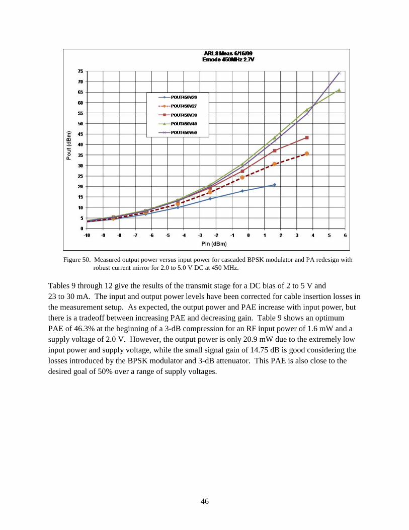
Figures 49 and 50 illustrate the relationship between PAE, and output power as input power increases over a DC voltage input range of 2.0 to 5.0 V. Output increases almost linearly until saturation, while PAE also reaches its optimum levels at higher input powers. Over the full range of DC input voltages, we see that this design is capable of providing 40% PAE and

45
20 dBm of output power. The output power and PAE were designed to be optimal at a particular supply voltage, but the design still works over a supply voltage range of about 2.0 to 5.0 V. Generally, the saturated output power increases with increasing supply voltage but the PAE will be optimal for a specific frequency, supply voltage, and RF input power level.
Figure 49. Measured PAE versus input power for cascaded BPSK modulator and PA redesign with bust current mirror for 2.0 to 5.0 V DC at 450 MHz.
0
5
10
15
20
25
30
35
40
45
50
-10 -9 -8 -7 -6 -5 -4 -3 -2 -1 0 1 2 3 4 5 6Pin
ARL8 Meas 6/16/09Emode 450MHz 2.7V
PAE450V20
PAE450V27
PAE450V30
PAE450V40
PAE450V50
46
Figure 50. Measured output power versus input power for cascaded BPSK modulator and PA redesign with robust current mirror for 2.0 to 5.0 V DC at 450 MHz.
Tables 9 through 12 give the results of the transmit stage for a DC bias of 2 to 5 V and 23 to 30 mA. The input and output power levels have been corrected for cable insertion losses in the measurement setup. As expected, the output power and PAE increase with input power, but there is a tradeoff between increasing PAE and decreasing gain. Table 9 shows an optimum PAE of 46.3% at the beginning of a 3-dB compression for an RF input power of 1.6 mW and a supply voltage of 2.0 V. However, the output power is only 20.9 mW due to the extremely low input power and supply voltage, while the small signal gain of 14.75 dB is good considering the losses introduced by the BPSK modulator and 3-dB attenuator. This PAE is also close to the desired goal of 50% over a range of supply voltages.

47
Table 9. Measured gain, PAE, and output power versus input power for cascaded BPSK modulator and PA for 2.0 V at 450 MHz.
Table 10 shows an optimum PAE of 45.6% at the beginning of a 3-dB compression for an RF input power of 2.5 mW and a supply voltage of 3.0V. The output power is ~43.4 mW, while the small signal gain increases to 15.75 dB. This PAE is close to the desired goal of 50%.
Table 10. Measured gain, PAE, and output power versus input power for cascaded BPSK modulator and PA for 3.0 V at 450 MHz.
Table 11 shows an optimum PAE of 44.6% at the beginning of a 3-dB compression for an RF input power of 4 mW and a supply voltage of 4.0 V. The output power is now 66.1 mW, while the small signal gain remains 15.75 dB. This PAE is close to the desired goal of 50% and the output power and gain are very good.

48
Table 11. Measured gain, PAE, and output power versus input power for cascaded BPSK modulator and PA for 4.0 V at 450 MHz.
Table 12 shows an optimum PAE of 40.3% at the beginning of a 3-dB compression for an RF input power of 4 mW and a supply voltage of 5.0 V. The output power is now 74.1 mW with reasonable but less than optimal efficiency, while the small signal gain is 15.4 dB.
Table 12. Measured gain, PAE, and output power versus input power for cascaded BPSK modulator and PA for 5.0 V at 450 MHz.
The measured results of the bare die tests for this design were very promising for all DC power input levels. From a supply voltage range of 2.0 to 5.0 V, the DC power consumption varies from 46 to 150 mW with a small signal gain from 14.75 to 15.75 dB and PAE from 46.3% to 40.3%. These values would be affected by the addition of the TR switch to the design, but these results give a good approximation to the behavior of a full design of the transmit stage. The input and output matches of the design are better than –8.0 dB and most cases are better than the goal of –10.0 dB. A phase difference of 174.5° for the two modulation states is within acceptable limits. Good performance of the transmit stage over a wide swing of input levels

49
means that this design can perform even as input power degrades as would be the case with an RFID battery supply or over an inconsistent power input if energy scavenging is used.
3.9 ARL09G24 – BPSK Modulator, PA, Narrowband LNA, and TR Switch Redesign with Current Mirror at 2.4 GHz
This is a redesign of the ARL07G24 described in section 3.7. The only changes are the addition of the current mirror to the design of the transmit stage and the new circuitry needed to make the control inputs of the BPSK modulator positive. The DC inputs for the BPSK modulator is 2.0 to 5.0 V to enable and 0.0 V to disable. Figure 51 shows the layout for the full booster chip design at 2.4 GHz.
Figure 51. Layout for 1.66x1.52 mm RFIC booster redesign with robust current mirror at 2.4 GHz.
Figures 52 and 53 show both modulation states have reasonable agreement between the simulated and the measured data for this design, although a gain of less than 10 dB is ~3 dB lower than the simulations. The input and output matches of both states are –9.5 dB or better, but the gains of 9.2 and 9.0 dB are much lower than desired. Some additional gain might be achieved by a redesign, but likely an additional gain stage is needed at these frequencies to boost the gain to ~20 dB.

50
Figure 52. Measured versus simulated S-parameters for transmit stage with robust current mirror for modulation state A at 2.4 GHz. Dashed lines are simulated and solid lines are measured data points.
Figure 53. Measured versus simulated S-parameters for transmit stage with robust current mirror for modulation state B at 2.4 GHz. Dashed lines are simulated and solid lines are measured data points.

51
Figure 54 compares the gain of chips ARL07G24 to that of this design. This design is a redesign of chip ARL07G24 with the addition of a current mirror and additional circuitry needed to convert the BPSK modulation inputs to a positive voltage. The new 2.4-GHz design improves the gain by 2.6 dB over the previous design though they should have been comparable. Both fall short of the desired gain for the transmit stage of this design.
Figure 54. Measured gain of ARL07G24 versus ARL09G24 for both modulation states of the transmit stage at 2.4 GHz.
Figure 55 compares the input match of chip ARL07G24 to this chip. The new chip yields comparable values for S11 at 2.4 GHz such that the values for both modulation states are within 1.0 dB of each other for both designs. An input match of –15.0 dB or better is excellent for this design.

52
Figure 55. Measured input match of ARL07G24 versus ARL09G24 for both modulation states of the transmit stage at 2.4 GHz.
Figure 56 compares the output match of design ARL07G24 to the design of this section. The redesigned chip yields a slight improvement over the original design. An S11 of –9.2 dB is ~2.0 dB better than the measured results of chip ARL07G24, and a value that is close to the –10.0 dB goal for this design.

53
Figure 56. Measured output match of ARL07G24 versus ARL09G24 for both modulation states of the transmit stage at 2.4 GHz.
Figure 57 shows the results of the measured versus simulated results for the S-parameters of the LNA when the chip is in receive mode. The measured results of the bare die tests for this narrowband design suffered from the same stability problems of nearly identical LNA from chip ARL07G24. A robust current mirror for both the LNA and PA were added to make the design operate over a supply voltage range of 2.0 to 5.0 V. Measurements of the LNA were made at a lower supply voltage before the gain increased to the point of becoming unstable. The results at the lower DC bias show a measured gain of only 7.5 dB, which is 7.0 dB of degradation over the simulated gain of 14.5 dB. As mentioned previously, this LNA design needs to be redesigned and checked with an EM simulator to avoid undesired coupling that could lead to instabilities.

54
Figure 57. Measured versus simulated S-parameters for receive stage at 2.4 GHz. Dashed lines are simulated and solid lines are measured data points.
Figure 58 shows the measured versus simulated results for the phase difference of the two modulation states of the BPSK modulator. At 2.4 GHz the measured phase difference is ~188.0° versus a simulated value of ~178.5°. This result is nearly identical to the BPSK modulator in ARL07G24, though the control inputs were modified from a negative voltage to a positive voltage. An ideal modulator would have a 180° phase difference between the two modulation states at the design frequency. A measured phase difference less than 10° is useful but could be improved with a subsequent redesign.

55
Figure 58. Measured versus simulated phase difference of the transmit stage redesign with robust current mirror for 3.0 V DC at 2.4 GHz. Blue is measured and brown is simulated data points.
Figure 59 illustrates the relationship between PAE, gain, and output power as input power increases. Output power increases almost linearly until saturation; PAE also reaches its optimum levels at higher input powers, and gain decreases as input power increases until saturation of the amplifier. Over the full range of input powers we see that this design is capable of providing 45% PAE and 17.5 dBm of output power with less than 3.0 dB of gain compression.

56
Figure 59. Measured PAE, output power, and gain versus input power for cascaded BPSK modulator and PA redesign with robust current mirror at 2.7 and 3.3 V DC at 2.4 GHz.
Tables 13 and 14 give the results of the transmit stage for a DC bias of 2.7 to 3.3 V. The input and output power levels have been corrected for cable insertion losses in the measurement setup. Table 13 shows an optimum PAE of 41.8% for an RF input power of 6 mW and table 14 shows an optimum PAE of 45.0% for an RF input power of 10 mW. The output power is 39.2 mW and 60.95 mW, respectively, while a small signal gain of ~10.5 dB is low for the desired goal of the transmit stage. Since the tables only show a 1.3- to 2.3-dB compression in gain, the values for optimum output power and PAE are expected to improve even more as the input power is increased up to the saturation level.

57
Table 13. Measured gain, PAE, and output power versus input power for cascaded BPSK modulator PA, and TR switch for 2.7 V at 2.4 GHz.
Table 14. Measured gain, PAE, and output power versus input power for cascaded BPSK modulator PA, and TR switch for 3.3 V at 2.4 GHz.
The measured results of the bare die tests for this design showed a need for improvement both in the transmit and receive stages. Although the PAE and output power of the transmit stage was good, the peak gain of ~10.5 dB was too low to produce the desired output power. Since PAE was almost 50% even before saturation of the amplifier was reached, there is room to tradeoff the PAE to increase the gain in this design. The LNA of the receive stage has to be redesigned to eliminate the stability problem and achieve the gain and NF goals.

58
3.10 ARL10M900 – BPSK Modulator, PA, Narrowband LNA, and TR Switch Redesign at 900 MHz
This is a redesign of the ARL03M900 described in section 3.3. The only changes are the addition of the current mirror to the design of the PA and modifying the BPSK modulator inputs to be a positive voltage. The DC input for the switch states of the BPSK modulator is about 2.0 to 5.0 V to enable and 0.0 V to disable. The footprint of the circuit is still 1.66x2.41 mm and figure 60 shows the layout for the full RFIC booster chip design at 900 MHz.
Figure 60. Layout for 1.66x2.41 mm narrowband RFIC booster redesign at 900 MHz.
Figures 61 and 62 show both modulation states have good agreement between the simulated and the measured data for this design. A gain of 13.0 and 12.8 dB, respectively, is acceptable for this design even though it is about a 1.0 dB less than the respective simulated values. The input and output matches of both states are –11.5 dB or better, and show slight improvements over the simulated values in all cases.

59
Figure 61. Measured versus simulated S-parameters for transmit stage with robust current mirror for modulation state A at 900 MHz. Dashed lines are simulated and solid lines are measured data points.
Figure 62. Measured versus simulated S-parameters for transmit stage with robust current mirror for modulation state B at 900 MHz. Dashed lines are simulated and solid lines are measured data points.

60
Figure 63 shows the measured versus simulated results for the phase difference of the two modulation states of the BPSK modulator. At 900 MHz, the measured phase difference is 183.3° versus a simulated value of ~180.0°. An ideal modulator would have a 180° phase difference between the two modulation states at the design frequency. Given the errors in measurement and process variation, a measured phase difference less than 10° should be within operational limits.
Figure 63. Measured versus simulated phase difference of the transmit stage redesign with robust current mirror at 900 MHz. Blue is measured and pink is simulated data points.
Figure 64 shows good agreement between the measured and simulated S-parameters of the LNA plus TR switch when the chip is in receive mode. The results show a measured gain of 12.9 dB, which is slightly less than the simulated value and is good for the low current narrowband LNA design. The input and output matches of –7.1 and –16.0 dB are acceptable.

61
Figure 64. Measured versus simulated S-parameters for receive stage at 900 MHz. Dashed lines are simulated and solid lines are measured data points.
Figure 65 shows the measured versus simulated performance of the LNA in terms of the gain and NF. At 900 MHz, the measured gain of the LNA matches simulation very well at ~13.25 dB. This also closely corresponds to the gain of figure 64. The measured NF of 3.0 dB at 900 MHz is acceptable although a NF of less than 2.0 dB is desired.
Figure 65. The behavior of the gain and NF for the LNA at 900 MHz.
0123456789
101112131415
0.6 1.1 1.6 2.1
dB
Freq
LNA10 2.7V NFADS
GainADS
NFCorr
GainCorr

62
Figure 66 illustrates the relationship between PAE, gain, and output power as input power increases. Output power increases almost linearly until saturation; PAE also reaches its optimum levels at higher input powers and gain decreases as input power increases until saturation of the amplifier. Over the measured range of input powers we see that this design is capable of providing 44% PAE and 16.0 dBm of output power at ~3.3 dB of gain compression.
Figure 66. Measured PAE, output power, and gain versus input power for cascaded BPSK modulator and PA redesign with robust current mirror for 2.7 V at 900 MHz.
Table 15 give the results of the transmit stage for a DC bias of 2.7 V. The input and output power levels have been corrected for cable insertion losses in the measurement setup. Table 15 shows an optimum PAE of 44.0% for an RF input power of 4 mW. The output power is 41.6 mW, while a small signal gain of 14.0 dB is comparable to the desired goal of 15.0 dB.

63
Table 15. Measured gain, PAE, and output power versus input power for cascaded BPSK modulator PA, and TR switch for 2.7 V at 2.4 GHz.
The measured results of the bare die tests for this design were very promising. A PAE of 44% was achievable for an RF input of less than 4 mW, and the small signal gain of 14.0 dB is also good. The LNA of the receive stage has acceptable input and output matches, although some improvement in the input match can be traded off for NF. The gain of 13.0 dB for the receive stage is also very good.
3.11 ARL11M450 – BPSK Modulator, PA, Narrowband LNA, TR Switch with Additional PA, and LNA Enable Input Redesign at 450 MHz
This is a redesign of the ARL06M450 described in section 3.6. The only change is the modifications to make the control inputs for the TR switch and BPSK modulator use positive voltages. The DC input switch states of the BPSK modulator are about 2.0 to 5.0 V to enable and 0 V to disable. The footprint of the circuit is still 1.66x2.41 mm and figure 67 shows the layout for the RFIC booster chip design at 450 MHz.

64
Figure 67. Layout for 1.66x2.41 mm RFIC booster redesign design at 450 MHz.
Figures 68 and 69 show both modulation states have good agreement between the simulated and the measured data for this design. A gain of 13.2 and 13.6 dB, respectively, is acceptable for this design even though it is ~1.5 dB less than the respective simulated values. The input and output matches of both states are –9.1 dB or better and are less than –12.0 dB in three of the four cases, which are all very good.

65
Figure 68. Measured versus simulated S-parameters for transmit stage for modulation state A at 450 MHz. Solid traces are the measured data points and dotted traces are the simulated values.
Figure 69. Measured versus simulated S-parameters for transmit stage for modulation state B at 450 MHz. Solid traces are the measured data points and dotted traces are the simulated values.
Figure 70 shows the measured versus simulated results for the phase difference of the two modulation states of the BPSK modulator. At 450 MHz, the measured phase difference is 184.7° versus a simulated value of ~180.0°. An ideal modulator would have a 180° phase difference between the two modulation states at the design frequency. Given the errors in measurement and process variation, a measured phase difference less than 10° should be within operational limits.
0.2 0.4 0.6 0.8 1.0 1.2 1.4 1.6 1.80.0 2.0
-20
-15
-10
-5
0
5
10
15
-25
20
freq, GHz
dB(S
(2,1
))
m1
dB(S
(1,1
))
m6
dB(S
(2,2
))
m10
dB(b
psk_
pa_4
50m
_2..S
(2,1
))[1
,::]
dB(b
psk_
pa_4
50m
_2..S
(1,1
))[1
,::]
dB(b
psk_
pa_4
50m
_2..S
(2,2
))[1
,::]
m1freq=dB(S(2,1))=13.636
450.0MHzm6freq=dB(S(1,1))=-12.761
450.0MHzm10freq=dB(S(2,2))=-14.706
450.0MHz
0.2 0.4 0.6 0.8 1.0 1.2 1.4 1.6 1.80.0 2.0
-25
-20
-15
-10
-5
0
5
10
15
-30
20
f req, GHz
dB(a
rl11b
30_m
s..S
(2,1
))
m7
dB(a
rl11b
30_m
s..S
(1,1
))
m8
dB(a
rl11b
30_m
s..S
(2,2
))
m11
dB(b
psk_
pa_4
50m
_2..S
(2,1
))[0,
::]dB
(bps
k_pa
_450
m_2
..S(2
,2))[
0,::]
dB(b
psk_
pa_4
50m
_2..S
(1,1
))[0,
::]
m7f req=dB(arl11b30_ms..S(2,1))=13.153
450.0MHzm8f req=dB(arl11b30_ms..S(1,1))=-9.075
450.0MHzm11f req=dB(arl11b30_ms..S(2,2))=-17.664
450.0MHz

66
Figure 70. Measured versus simulated phase difference of the transmit at 450 MHz. Blue is measured and pink is simulated data points.
Figure 71 shows the results of the measured versus simulated results for the S-parameters of the LNA for the chip’s receive mode. The results show a measured gain of 8.8 dB. The output match of –13.7 is good, as is the input match of –12.9 dB.

67
Figure 71. Measured versus simulated S-parameters for receive stage at 450 MHz. Solid traces are the measured data points and dotted traces are the simulated values.
Figure 72 shows the results of the measured versus simulated results for the S-parameters of the LNA for the isolation between the transmit and receive isolation when the TR switch is set to transmit. The results show a measured gain of –12.3 dB, which is over 20 dB of isolation. The output match of –12.3 dB is good, but the input match of –4.0 dB is poor as the LNA is not in receive mode.
Figure 72. Measured versus simulated S-parameters for receive stage at 450 MHz with TR switch set to transmit. Solid traces are the measured data points and dotted traces are the simulated values.
0.5 1.0 1.50.0 2.0
-15
-10
-5
0
5
10
-20
15
freq, GHz
dB(S
(2,1
))
m4
dB(S
(1,1
))
m6dB(S
(2,2
))
m2
dB(b
psk_
pa_4
50m
_11.
.S(3
,3))
dB(b
psk_
pa_4
50m
_11.
.S(2
,2))
dB(b
psk_
pa_4
50m
_11.
.S(3
,2))
m4freq=dB(S(2,1))=8.774
450.0MHz
m6freq=dB(S(1,1))=-12.931
450.0MHzm2freq=dB(S(2,2))=-13.684
450.0MHz
0.5 1.0 1.50.0 2.0
-25
-20
-15
-10
-5
-30
0
freq, GHz
dB(S
(2,1
))
m4
dB(S
(1,1
))
m6
dB(S
(2,2
))
m2
dB(b
psk_
pa_4
50m
_11.
.S(3
,3))
dB(b
psk_
pa_4
50m
_11.
.S(2
,2))
dB(b
psk_
pa_4
50m
_11.
.S(3
,2))
m4freq=dB(S(2,1))=-10.992
450.0MHz
m6freq=dB(S(1,1))=-3.976
450.0MHzm2freq=dB(S(2,2))=-12.267
450.0MHz

68
Figure 73 shows the measured versus simulated performance of the LNA in terms of the gain and NF. At 450 MHz, the measured gain of the LNA is 10.0 dB, which is lower than the desired value of 15.0 dB, and a NF of ~4.0 dB at 500 MHz shows that this design does not perform as expected from the simulations. There is a lot of ripple in the NF measurement but it does start to match the simulations above 700 MHz.
Figure 73. The behavior of the gain and NF for the LNA at 450 MHz.
Figure 74 illustrates the relationship between PAE, gain, and output power as input power increases. Output power increases almost linearly until saturation; PAE also reaches its optimum levels at higher input powers and gain decreases as input power increases until there is saturation of the amplifier. Over the measured range of input powers we see that this design is capable of providing 42.5% PAE and 16.0 dBm of output power.
0123456789
101112
0.2 0.4 0.6 0.8 1.0 1.2 1.4 1.6
dB
Freq
LNA11 3V
GainADS
NFADS
NFCorrv3
GainCorrv3

69
Figure 74. Measured PAE, output power, and gain versus input power for cascaded BPSK modulator and PA redesign with robust current mirror for 2.7 V at 900 MHz.
Tables 16 and 17 give the results of the transmit stage for a DC supply of 2.7 and 3.0 V. The input and output power levels have been corrected for cable insertion losses in the measurement setup. Table 16 shows an optimum PAE of 42.3% for an RF input power of 4 mW and table 17 shows an optimum PAE of 42.3% for an RF input power of 4 mW. The output power is 31.95 and 40.2 mW, respectively, while a small signal gain of approximately 13.6 and 14.4 dB for both tables is near the desired goal for the transmit stage.
Table 16. Measured gain, PAE, and output power versus input power for cascaded BPSK modulator PA, and TR switch for 2.7 V at 450 MHz.

70
Table 17. Measured gain, PAE, and output power versus input power for cascaded BPSK modulator PA, and TR switch for 3.0 V at 450 MHz.
The measured results of the bare die tests for this design were promising for the transmit stage, but showed a need for improvement in terms of the receive stage. An acceptable gain was achieved as well as a good PAE measurement at lower DC input powers than in previous designs. However, the optimal output power was somewhat lower than in previous designs due to loss from the TR switch. The low current narrowband LNA of the receive stage had good input and output matches, a low gain of ~10 dB, and a poor NF, which will introduce additional noise into the amplified signal.
3.12 ARL12M450 – BPSK Modulator, PA, and TR Switch Design at 450 MHz
This design is a narrowband cascaded BPSK modulator, PA, and TR switch designed at 450 MHz on a 1.66x1.52 mm die. There was not enough room to add the ground-signal-ground (GSG) pads needed to measure the receive path for the TR switch individually. This TR switch may have higher insertion loss than the other 450-MHz design because the capacitors are smaller due to the limited area available in the die. This design provided the designers with a way to gauge the effect of the TR switch on the transmit stage without having to deal with potential degradation from isolation issues introduced with the addition of the receive mode to the design. This provides a good metric to measure the full RFIC booster chip design against ARL08M450. Figure 75 shows the layout of the design that was used for the simulations.

71
Figure 75. Layout for cascaded BPSK modulator, PA, and TR switch at 450 MHz.
Figures 76 and 77 show both modulation states have good agreement between the simulated and the measured data for this design. A gain of 14.1 and 15.7 dB, respectively, is very good for this design. The input and output matches of both states are –9.0 dB or better and are similar to the simulated values.
Figure 76. Measured versus simulated S-parameters for transmit stage for modulation state A at 450 MHz. Dashed lines are simulated and solid lines are measured data points.
0.2 0.4 0.6 0.8 1.0 1.2 1.4 1.6 1.80.0 2.0
-20
-15
-10
-5
0
5
10
15
-25
20
freq, GHz
dB(S
(2,1
))
m1
dB(S
(1,1
))
m6
dB(S
(2,2
))
m10
dB(b
psk_
pa_4
50m
_2..S
(2,1
))[1
,::]
dB(b
psk_
pa_4
50m
_2..S
(1,1
))[1
,::]
dB(b
psk_
pa_4
50m
_2..S
(2,2
))[1
,::]
m1freq=dB(S(2,1))=14.13
450.0MHzm6freq=dB(S(1,1))=-15.83
450.0MHzm10freq=dB(S(2,2))=-15.15
450.0MHz

72
Figure 77. Measured versus simulated S-parameters for transmit stage for modulation state B at 450 MHz. Dashed lines are simulated and solid lines are measured data points.
Figure 78 shows the measured versus simulated results for the phase difference of the two modulation states of the BPSK modulator. At 450 MHz, the measured phase difference is 171.0° versus a simulated value of ~179.0°. An ideal modulator would have a 180° phase difference between the two modulation states at the design frequency. Given the errors in measurement and process variation, a measured phase difference less than 10° should be within operational limits.

73
Figure 78. Measured versus simulated phase difference of the transmit stage redesign with robust current mirror at 900 MHz. Blue is measured and pink is simulated data points.
The measured results of the bare die tests for this design were promising. A very good gain of ~15.0 dB was achieved for both modulation states. The input and output matches were within or better than acceptable limits as was the measured phase difference of the modulation states.
3.13 ARL13M450 – Individual BPSK Modulator and PA Redesign without Current Mirror at 450 MHz
This is a test chip based on the ARL08M450 design described in section 3.8. Additional GSG probe pads were added so that the BPSK modulator and PA performances could be measured individually. The current mirror is not a part of this design as it was for the ARL08M450 design, but the BPSK modulation inputs use positive voltages. Figure 79 shows the layout for the BPSK modulator and PA at 450 MHz.

74
Figure 79. Layout of cascaded BPSK modulator and PA design with additional GSC pads at 450 MHz.
Figure 80 shows the measured results of the bare die versus the simulated results for the gain of the PA at 450 MHz. The measured results at 2.7 V show a gain of 18.5 dB, and ideally the PA would achieve a gain of 20.0 dB before additional losses were introduced. The measurements match simulation very well considering the blue and pink plots are simulated gain at higher DC supply values than that of the measured data.

75
Figure 80. Measured versus simulated gain for PA at 450 MHz. The red traces are measured data points at 2.7 V, while the other traces are simulations at 2.5 and 3.0 V.
Figure 81 shows the measured results of the bare die versus the simulated results for the input match of the PA at 450 MHz. The measured results at 2.7 V match the simulation very closely, but an S11 of –4.7 dB is poor.
Figure 81. Measured versus simulated input match for PA at 450 MHz. Red is the measured data points.

76
Figure 82 shows the measured results of the bare die versus the simulated results for the output match of the PA at 450 MHz. The measured results at 2.7 V match the simulation very closely, and a S11 of –8.5 dB is an improvement over the poor input match and close to a desired goal of –10.0 dB.
Figure 82. Measured versus simulated output match for PA at 450 MHz. The red line is measured data.
Figures 83 and 84 show the measured results of the bare die for DC input voltages of 1.8 to 5.0 V for the input and output match of the BPSK modulator at 450 MHz. The measured results across all DC supply ranges match very closely and are better than –10.0 dB for all cases in both modulation states.

77
Figure 83. Measured input match for BPSK modulator in modulation state A from 1.8 to 5.0 V DC input at 450 MHz.
Figure 84. Measured input match for BPSK modulator in modulation state B from 1.8 to 5.0 V DC input at 450 MHz.

78
Figures 85 and 86 show the measured results of the bare die for DC input voltages of 1.8 to 5.0 V for the insertion loss of the BPSK modulator at 450 MHz in both modulation states. The measured results across all DC supply ranges match closely, but there is about a 0.4-dB improvement at the DC supply levels above 2.5 V. Both modulation states show an insertion loss of –2.0 to –2.5 dB, which is acceptable.
Figure 85. Measured insertion loss for BPSK modulator in modulation state A from 1.8 to 5.0 V DC input at 450 MHz.

79
Figure 86. Measured insertion loss for BPSK modulator in modulation state B from 1.8 to 5.0 V DC input at 450 MHz.
Figure 87 shows the measured versus simulated results for the phase difference of the two modulation states of the BPSK modulator. At 2.4 GHz, the magnitude of the measured phase difference is 180.0° versus a simulated value of ~177.0°. An ideal modulator would have a 180° phase difference between the two modulation states at the design frequency, and the measured data actually show an improvement over the simulated data.

80
Figure 87. Measured versus simulated phase difference of the transmit stage redesign with robust current mirror at 2.4 GHz. Green is measured and purple is simulated data points.
Figure 88 illustrates the relationship between PAE, gain, and output power as input power increases. Output power increases almost linearly until saturation; PAE reaches its optimum levels at higher input powers and gain decreases as input power increases until saturation of the amplifier. Over the measured range of input powers we see that this design is capable of providing 50% PAE and 17.2 dBm of output power.

81
Figure 88. Measured PAE, output power, and gain versus input power for PA for 2.7 V at 450 MHz.
Tables 18 and 19 give the results of the transmit stage for a DC bias of 2.7 and 3.0 V. The input and output power levels have been corrected for cable insertion losses in the measurement setup. Table 18 shows an optimum PAE of 52.1% for an RF input power of 1 mW and table 19 shows an optimum PAE of 50.6% for an RF input power of 1 mW. The output power is 41.7 and 52.5 mW, respectively, while a small signal gain of 20.8 and 21.3 dB for both supply voltages meets the design goal. A PAE of better than 50% and a gain of better than 20.0 dB is very good for an RF input power of 1 mW, but this is before losses introduced by the BPSK modulator, attenuator, and TR switch are taken into account.

82
Table 18. Measured gain, PAE, and output power versus input power for PA at 2.7 V and 2.4 GHz.
Table 19. Measured gain, PAE, and output power versus input power for PA at 3.0 V and 2.4 GHz.
The measured results of the bare die tests for this design showed very good results for the PA and BPSK individually. The PAE, output power, and gain of the PA are all very good and meet the design goals. Insertion loss, input match, output match and phase difference of the BPSK modulator show that it meets the design goals as well, though the insertion loss could be improved.
3.14 ARL14G24 – BPSK Modulator, PA, Narrowband LNA, and TR Switch Redesign with Current Mirror at 2.4 GHz
This is a test chip based on the ARL09G24 design described in section 3.9. Additional GSG probe pads were added so that the performances of each element could be measured individually. The current mirror is not a part of this design as it was for the ARL09G24 design, but the BPSK modulation inputs use positive voltages. The footprint of the circuit is still 1.66x1.52 mm and figure 89 shows the layout for the RFIC booster chip at 2.4 GHz.

83
Figure 89. Layout of 1.66x1.52 mm RFIC design with additional GSC pads at 2.4 GHz.
Figure 90 shows the measured results of the bare die versus the simulated results for the gain of the PA at 2.4 GHz. The measured results at 2.7 V show a gain of 14.0 and 15 dB at 3.0 V and match the simulation very well.
Figure 90. Measured versus simulated gain for PA at 2.4 GHz. The blue and red traces are measured data.

84
Figure 91 shows the measured results of the bare die versus the simulated results for the input match of the PA at 2.4 GHz. The measured results at 3.0 V match the simulated data almost exactly. This input match is less than the desired –10 dB return loss goal, but gain, bandwidth, and return loss are part of the design tradeoffs.
Figure 91. Measured versus simulated input match for PA at 2.4 GHz. The red trace is the measured data.
Figure 92 shows the measured results of the bare die versus the simulated results for the output match of the PA at 2.4 GHz. The measured results at 3.0 V show an S22 of better than –10 dB meeting the desired goal.

85
Figure 92. Measured versus simulated output match for PA at 2.4 GHz. The red trace is the measured data.
Figure 93 shows the measured results of the bare die versus the simulated results for the S-parameters of the BPSK modulator at 2.4 GHz. The measured results for both modulation states match very closely and an insertion loss of –1.9 dB, an input match of –13.9 dB, and an output match of –16.5 dB are all excellent measurements for this design.

86
Figure 93. Measured S-parameters for BPSK modulator in both modulation states at 450 MHz.
Figure 94 shows the measured versus simulated results for the phase difference of the two modulation states of the BPSK modulator. At 2.4 GHz, the magnitude of the measured phase difference is 186.0° versus a simulated value of ~180.0°. An ideal modulator would have a 180.0° phase difference between the two modulation states at the design frequency. Given the errors in measurement and process variation, a measured phase difference less than 10° should be within operational limits.

87
Figure 94. Measured versus simulated phase difference of the transmit stage redesign with robust current mirror at 2.4 GHz. Green is measured and purple is simulated data points.
Figure 95 shows the LNA at 2.4 GHz. There was an inadvertent design flaw that bypassed a matching capacitor for the input match. Surprisingly, this layout flaw in the test circuit led to a stable LNA design, which matches the re-simulations, once the series matching capacitor is omitted.

88
Figure 95. Measured versus re-simulated s-parameters for the LNA with an error in the input match layout at 2.4 GHz. The solid traces are measured data and the dotted traces are simulations.
Figure 96 illustrates the relationship between PAE, gain, and output power as input power increases. Output power increases almost linearly until saturation; PAE also reaches its optimum levels at higher input powers and gain decreases as input power increases until saturation of the amplifier. Over the measured range of input powers, we see that this design is capable of providing 62.5% PAE and 18.0 dBm of output power.
2 3 41 5
-20
-15
-10
-5
0
5
-25
10
freq, GHz
dB(S
(2,1
))
m4
dB(S
(1,1
))
m6
dB(S
(2,2
))
m2
dB(ln
a240
0m..S
(2,2
))dB
(lna2
400m
..S(1
,1))
dB(ln
a240
0m..S
(2,1
))
m4freq=dB(S(2,1))=8.905
2.400GHz
m6freq=dB(S(1,1))=-1.950
2.400GHzm2freq=dB(S(2,2))=-14.95
2.400GHz

89
Figure 96. Measured PAE, output power, and gain versus input power for cascaded BPSK modulator and PA redesign with robust current mirror for 2.7 V at 900 MHz.
Tables 20 and 21 give the results of the transmit stage for a DC supply of 2.7 and 3.0 V. The input and output power levels have been corrected for cable insertion losses in the measurement setup. Table 20 shows an optimum PAE of 62.6% for an RF input power of 4 mW and table 21 shows an optimum PAE of 59.7% for an RF input power of 4 mW. The output power is 57.4 and 69.7 mW, respectively, while a small signal gain of ~15.0 dB for both supply voltages meets the design goal. Since the tables only show a 2.0- to 2.5-dB compression in gain, the values for optimum output power and PAE are expected to improve even more as the input power is increased up to the saturation level.

90
Table 20. Measured gain, PAE, and output power versus input power for PA at 2.7 V and 2.4 GHz.
Table 21. Measured gain, PAE, and output power versus input power for PA at 3.0 V and 2.4 GHz.
The measured results of the bare die tests for this design showed a need for improvement in terms of both the input and output matches of the transmit stage. The PAE, output power, and peak gain are excellent for the PA. A design flaw occurred in the layout of the LNA in this test circuit but that helped isolate the stability problem in the actual design. The measurements of the BPSK design indicate that it functions very well.
4. Performance Summary
Table 22 summarizes the performance of the various designs. The first column is the design number followed by the design frequency (450, 900, or 2400 MHz). The next column contains a check mark for having a BPSK modulator—note that all designs include this item. PAE is given as a percentage (%) under the PA column. The NF (in dB) is given under the LNA column. The

91
other columns designate whether there is a TR switch and the voltage polarity of the BPSK and TR switch control signals. A minus (–) indicates negative voltages (0, –3 V typically) and a plus (+) indicates positive voltages (0, +3 V typically). The column “Enb” designates whether the circuit contains a gate enable control input or not. If there is a robust current mirror bias to allow a range of supply voltages, it is indicated in “Robust DC” column All designs fit in either a 3x3 mm quad flat non-leaded (QFN) package or a 4x4 mm QFN package, as designated in the PKG column. Lastly, a few notes are added in the final column. Additional performance checks for the various designs will be performed on the packaged devices. Package effects are expected to be minimal, particularly for the 450- and 900-MHz designs.
Table 22. A summary of the performance of the various designs.
Design Freq BPSK
PA LNA TRS ContBPSK
ContTRS
Enb RobustDC
PKG Notes
1 900 √ √ 58 √ 2.1 − 3x3 Sep. BB LNA
2 450 √ √ 43 − 3x3 See #8
3 900 √ √ 31 √ 3.5 √ − + 4x4 OK
4 900 √ √ 26 √ 2.5 √ − − 3x3 Stable LNA/PA
5 450 √ √ 38 √ √ − + 4x4 Bad TRS Layout
6 450 √ √ 40 √ √ − + yes 4x4 See #11
7 2.4G √ √ √ √ − + 3x3 See #9, Bad LNA
8 450 √ √ 45 √ + + yes 3x3 Good Perform.
9 2.4G √ √ 45 √ √ + + 3x3 Bad LNA
10 900 √ √ 44 √ 3.1 √ + + yes 4x4 Good Perform.
11 450 √ √ 41 √ 3.4 √ + + yes 4x4 Good Perform.
12 450 √ √ √ + + yes 3x3 #8 w/ TRS
13 450 √ √ 52 + 3x3 #8 Test Chip
14 2.4G √ √ 63 √ √ + + 3x3 #9 Test Chip
15 18G NA Worked, Bad C.

92
5. Conclusions
The purpose of the RFIC booster chip is to increase the performance of RF front ends based on commercial-off-the-shelf (COTS) parts. The booster chip should be customized to the desired power supply voltage, output power levels required, NF, and gain to improve existing systems but minimize complexity by simply inserting the booster chip between the transceiver and antenna.
Multiple versions of some simple circuits were fabricated in GaAs because of the excellent performance of GaAs for switches, LNAs, and very efficient PAs. The frequencies of interest were chosen as 450 MHz, 900 MHz, and 2.4 GHz as these covered several commercial bands of operation. Various combinations of LNAs, a high speed BPSK modulator, an efficient customized PA, and a low loss TR switch were combined on the first design pass to test the designs and learn enough through measurements to tweak the first pass designs into final RFIC chips. These final designs could be customized with the desired combinations of components and optimized for the particular specifications desired.
Overall, the designs were very successful and achieved the goal of this effort. The one disappointment may have been the stability problems of the 2.4-GHz LNA, but a lesson was learned in that the stability problem can be predicted by simulations with Sonnet EM software in addition to using ADS and MWO simulations. The TR switch and BPSK modulator insertion losses were likewise a little higher than expected, but these results can be used to redesign those circuits for lower loss in future designs. Also, the effect of the TR switch was not factored fully into the design of the PA and LNAs. These effects can be incorporated into optimizing the amplifiers at the system level, and not just into ideal 50-ohm input and outputs. Next, the designs will be tested in packages, noting any effects from the package parasitics that could also be factored into optimized future second pass designs. Additionally, some kind of system-level test needs to be performed with a packaged device and integrated into an RF front end to show the improvements possible at the system level. There might be some additional refinements to any optimized second pass designs based on lessons learned in the system level test.
6. Path Forward
The most promising designs from this round of testing need to be packaged and retested to verify that the packaging does not introduce any great degradation to the performance of the design. These packaged chips then need to be integrated into an evaluation circuit to test the performance of the booster chip during actual RF transmission and reception, and also to determine how easy it is to control the DC inputs with routed circuit lines on a printed circuit

93
board (PCB). Performance will be based on whether the chip significantly increases the transmission range between two wireless nodes in comparison to the same RF front end but without the RFIC booster chip included.

94
List of Symbols, Abbreviations, and Acronyms
ADS Agilent Design System
BPSK binary phase shift keying
COTS commercial off the shelf
DRC design rule checks
EM electromagnetic
GaAs gallium arsenide
GSG ground-signal-ground
LNA low-noise amplifier
LVS layout vs. schematic
MWO Microwave Office
NF noise figure
PA power amplifier
PAE power added efficiency
PCB printed circuit board
QFN quad flat non-leaded
RF radio frequency
RFIC rf integrated circuit
RFID RF identification
SiGe silicon germanium
TR transmit/receive

95
No. of Copies Organization 1 ADMNSTR ELEC DEFNS TECHL INFO CTR ATTN DTIC OCP 8725 JOHN J KINGMAN RD STE 0944 FT BELVOIR VA 22060-6218 1 US ARMY RSRCH LAB ATTN RDRL CIM G T LANDFRIED BLDG 4600 ABERDEEN PROVING GROUND MD 21005-5066 1 CD OFC OF THE SECY OF DEFNS ATTN ODDRE (R&AT) THE PENTAGON WASHINGTON DC 20301-3080 1 US ARMY INFO SYS ENGRG CMND ATTN AMSEL IE TD A RIVERA FT HUACHUCA AZ 85613-5300 1 COMMANDER US ARMY RDECOM ATTN AMSRD AMR W C MCCORKLE 5400 FOWLER RD REDSTONE ARSENAL AL 35898-5000 1 CD CERDEC, I2WD ATTN BOB GROSS ABERDEEN PROVING GROUND MD 21005-5066 10 US ARMY RSRCH LAB ATTN IMNE ALC HRR MAIL & RECORDS MGMT ATTN RDRL CIM L TECHL LIB ATTN RDRL CIM P TECHL PUB
ATTN RDRL SER E R DEL ROSARIO
ATTN RDRL SER E E VIVEIROS ATTN RDRL SER E G MITCHELL (2 COPIES) ATTN RDRL SER E J PENN (2 COPIES) ATTN RDRL SER E J WILSON ADELPHI MD 20783-1197 TOTAL: 16 (13 HCS, 1 ELEC, 2 CDS)

96
INTENTIONALLY LEFT BLANK.


