Since Moore’s law driven scaling of planar MOSFETs faces formidable challenges in the nanometer regime, FinFETs and TrigateFETs have emerged as their successors. Owing to the presence of multiple (two/three) gates, FinFETs/Trigate FETs are able totackle short-channel effects (SCEs) better than conventional planar MOSFETs at deeply scaled technology nodes and thus enablecontinued transistor scaling. In this paper, we review research on FinFETs from the bottommost device level to the topmostarchitecture level. We survey different types of FinFETs, various possible FinFET asymmetries and their impact, and novel logic-level and architecture-level tradeoffs offered by FinFETs. We also review analysis and optimization tools that are available forcharacterizing FinFET devices, circuits, and architectures.
1. Introduction
Relentless scaling of planar MOSFETs over the past fourdecades has delivered ever-increasing transistor density andperformance to integrated circuits (ICs). However, continu-ing this trend in the nanometer regime is very challengingdue to the drastic increase in the subthreshold leakagecurrent (𝐼off ) [1–3]. Due to the very narrow channel lengthsin deeply scaled MOSFETs, the drain potential begins toinfluence the electrostatics of the channel and, consequently,the gate loses adequate control over the channel. As a result,the gate is unable to shut off the channel completely inthe off-mode of operation, which leads to an increased𝐼off between the drain and the source. The use of thinnergate oxides and high-k dielectric materials helps alleviatethis problem by increasing the gate-channel capacitance.However, thinning of gate oxides is fundamentally limitedby the deterioration in gate leakage and gate-induced drainleakage (GIDL) [4–6]. Multiple-gate field-effect transistors(MGFETs), which are an alternative to planar MOSFETs,demonstrate better screening of the drain potential from thechannel due to the proximity of the additional gate(s) tothe channel (i.e., higher gate-channel capacitance) [7–12].This makes MGFETs superior to planar MOSFETs in short-channel performance metrics, such as subthreshold slope
(𝑆), drain-induced barrier lowering (DIBL), and thresholdvoltage (𝑉th) roll-off. Improvement in these metrics impliesless degradation in the transistor’s𝑉th with continued scaling,which in turn implies less degradation in 𝐼off .
So far, we have referred to planarMOSFETs built on bulk-Si wafers (or bulk MOSFETs) as planar MOSFETs. Fully-depleted silicon-on-insulator (FDSOI) MOSFETs (planarMOSFETs built atop SOI wafers) avoid the extra leakagepaths from the drain to source by getting rid of the extrasubstrate beneath the channel [13, 14]. Their performancemetrics are comparable with those of double-gate FETs(DGFETs), which are MGFETs with two gates. Both offerreduced junction capacitance, higher 𝐼on/𝐼off ratio, better 𝑆,and improved robustness against random dopant fluctuation(RDF). However, DGFETs have a more relaxed constrainton channel thickness, which makes DGFETs more scalablethan FDSOI MOSFETs in the long run [15, 16]. Also, DGFETstructures can be built on bulk-Si wafers, as well, whichmakesDGFETs more attractive to foundries that do not want toswitch to an SOI process [17, 18].
Among all MGFETs, FinFETs (a type of DGFET) andTrigate FETs (another popularMGFETwith three gates) haveemerged as the most desirable alternatives to MOSFETs dueto their simple structures and ease of fabrication [19–27].Two or three gates wrapped around a vertical channel enable
Hindawi Publishing CorporationAdvances in ElectronicsVolume 2014, Article ID 365689, 21 pageshttp://dx.doi.org/10.1155/2014/365689
2 Advances in Electronics
easy alignment of gates and compatibility with the standardCMOS fabrication process. In Trigate FETs, an additionalselective etching step of the hard mask is involved in orderto create the third gate on top of the channel. Although thisthird gate adds to process complexity, it also leads to someadvantages like reduced fringe capacitances and additionaltransistor width [28–30].
FinFET/Trigate devices have been explored thoroughlyin the past decade. A large number of research articles havebeen published that demonstrate the improved short-channelbehavior of these devices over conventional bulk MOSFETs[19–22, 31–33]. Many researchers have presented novel circuitdesign styles that exploit different kinds of FinFETs [34–48]. Researchers have also explored various symmetric andasymmetric FinFET styles and used them in hybrid FinFETlogic gates and memories [49–66]. Newer architectures forcaches, networks-on-chip (NoCs), and processors based onsuch logic gates and memories have also been explored [67–74]. In spite of these advancements in FinFET research,articles that provide a global view of FinFETs from thedevice level to the topmost architecture level are scarce.Mishra et al. provided such a view at the circuit level [75].However, FinFETs are not covered at other levels of the designhierarchy. Also, at the circuit level, much progress has beenmade since the publication of that book chapter. Our articleis aimed at a wide range of readers: device engineers, circuitdesigners, and hardware architects. Our goal is to provide aglobal view of FinFET concepts spanning the entire IC designhierarchy.
The paper is organized as follows. In Section 2, wereview the different types of FinFETs and possible asym-metries that can be designed into their structures. We alsodiscuss the sources of process variations in FinFETs andtheir impact on FinFET performance. We discuss FinFETprocess simulation, device simulation, and compact modelsin Section 3. We describe novel FinFET inverter (INV)and NAND gates, flip-flops, latches, static random-accessmemory (SRAM), and dynamic random-access memory(DRAM) cells in Section 4. In Section 5, we discuss circuit-level analysis and optimization methodologies and a novelinterconnect scheme that leverages FinFETs.We then presenta survey of process-voltage-temperature (PVT) variation-aware architecture-level simulation tools in Section 6 andconclude in Section 7.
2. FinFETs
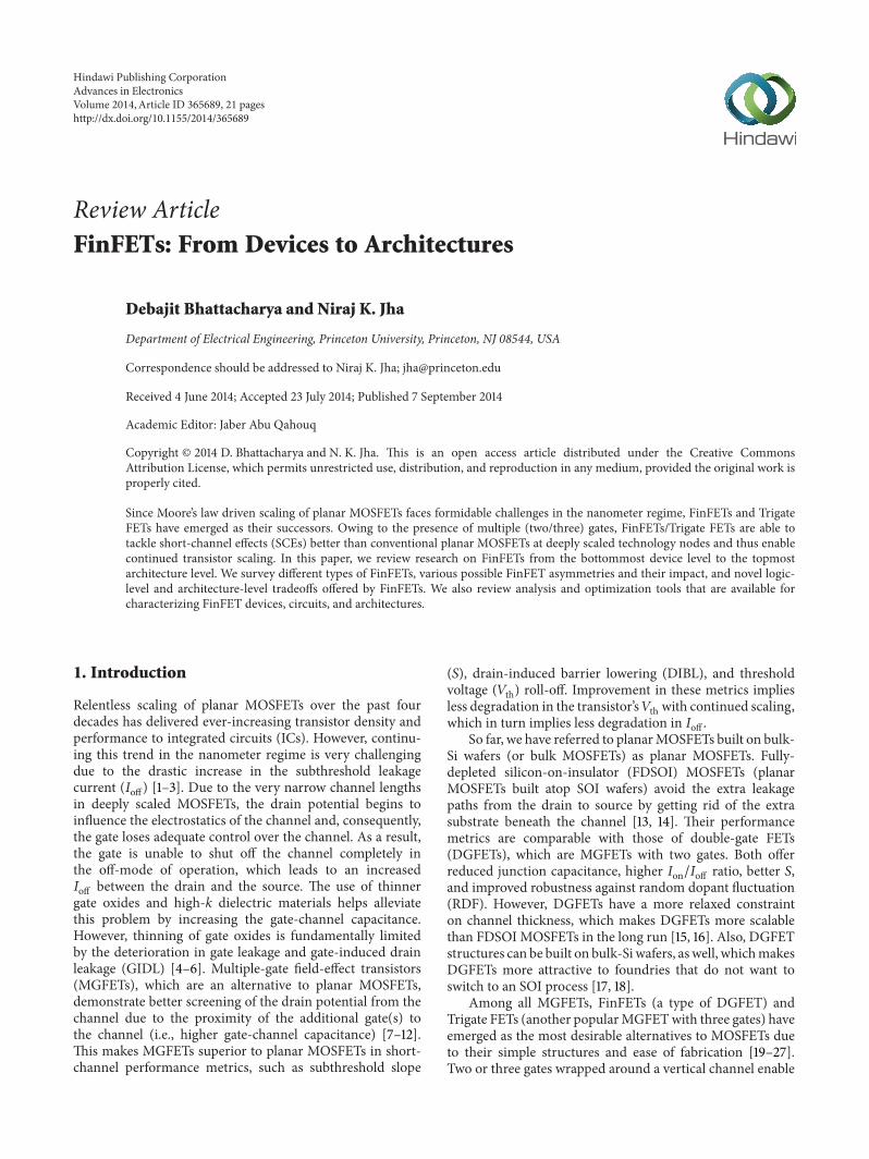
In 1989,Hisamato et al. fabricated a double-gate SOI structurewhich they called a fully-depleted lean channel transistor(DELTA) [76]. This was the first reported fabrication ofa FinFET-like structure. FinFETs have attracted increasingattention over the past decade because of the degradingshort-channel behavior of planar MOSFETs [19–24]. Figure 1demonstrates the superior short-channel performance ofFinFETs over planarMOSFETs with the same channel length.Figure 2 shows a conventional planarMOSFET and a FinFET.While the planar MOSFET channel is horizontal, the FinFETchannel (also known as the fin) is vertical. Hence, the height
DIB
L (m
V/V
)
400
350
300
250
200
150
100
50
0
LEFF (nm)15 25 35 45 55
Double-gate
Single-gate/bulk
Subt
hres
hold
swin
g (m
V/d
ecad
e)
120
100
80
60
40
20
0
Figure 1: DIBL and subthreshold swing (𝑆) versus effective channellength for double-gate (DG) and bulk-silicon nFETs.TheDG deviceis designed with an undoped body and a near-mid-gap gate material[12].
of the channel (𝐻FIN) determines the width (𝑊) of theFinFET. This leads to a special property of FinFETs knownas width quantization. This property says that the FinFETwidth must be a multiple of 𝐻FIN, that is, widths can beincreased by using multiple fins. Thus, arbitrary FinFETwidths are not possible. Although smaller fin heights offermore flexibility, they lead to multiple fins, which in turnleads to more silicon area. On the other hand, taller finslead to less silicon footprint, but may also result in structuralinstability. Typically, the fin height is determined by theprocess engineers and is kept below four times the finthickness [77, 78].
Although FinFETs implemented on SOI wafers are verypopular, FinFETs have also been implemented on con-ventional bulk wafers extensively [79–81]. Figure 3 showsFinFETs implemented on bulk and SOI wafers. Unlike bulkFinFETs, where all fins share a common Si substrate (alsoknown as the bulk), fins in SOI FinFETs are physicallyisolated. Some companies prefer the bulk technology becauseit is easier tomigrate to bulk FinFETs from conventional bulkMOSFETs. However, FinFETs on both types of wafers arequite comparable in terms of cost, performance, and yield,and it is premature to pick a winner. From this point on, ourdiscussion will be limited to SOI FinFETs unless otherwisementioned.
Trigate FETs, referred to interchangeably as FinFETs, inthis paper so far, are a variant of FinFETs, with a third gateon top of the fin. Intel introduced Trigate FETs at the 22 nmnode in the Ivy-Bridge processor in 2012 [28, 82]. Figure 4shows a Trigate FET along with a FinFET. The thickness ofthe dielectric on top of the fin is reduced in Trigate FETs inorder to create the third gate. Due to the presence of the thirdgate, the thickness of the fin also adds to the channel width.Hence, Trigate FETs enjoy a slight width advantage overFinFETs. Trigate FETs also have less gate-source capacitancecompared to FinFETs due to additional current conduction atthe top surface, but this advantage is diminished by increasedparasitic resistance [29].
Advances in Electronics 3
Source
GateDrain
WL
Gate dielectric
(a)
Source
Drain
L
Gate dielectric
Gate 1
Gate 2
HFIN
(b)
Figure 2: Structural comparison between (a) planar MOSFET and (b) FinFET.
Source
Gate 1
Gate 2
Drain
Silicon substrate
(a)
Source
Gate 1
Gate 2
Drain
Silicon substrate
Buried oxide
(b)
Figure 3: Structural comparison between (a) bulk and (b) SOI FinFETs.
Yang and Fossum compared Trigate FETs and FinFETsand argued that FinFETs are superior to Trigate FETs inthe long run [83]. They showed that although undopedTrigate FETs may enjoy more relaxed body thickness, theyare not competitive with FinFETs in SCE metrics. Whentrying to achieve comparable SCE metrics, Trigate FETs losethe scaling advantage and suffer from significant layout areadisadvantage. However, like the bulk versus SOI debate, it isalso premature to declare a clear winner between FinFETsand Trigate FETs. From this point onwards, we will considerFinFETs only unless stated otherwise.
FinFETs can be fabricated with their channel alongdifferent directions in a single die. Fabrication of planarMOSFET channels along any crystal plane other than ⟨100⟩is difficult due to process variations and interface traps [36,84]. However, FinFETs can be fabricated along the ⟨110⟩plane as well. This results in enhanced hole mobility. ⟨110⟩-oriented FinFETs can be fabricated by simply rotating thetransistor layout by 45∘ in the plane of a ⟨100⟩ wafer [85].Thus, nFinFETs implemented along ⟨100⟩ and pFinFETsalong ⟨110⟩ lead to faster logic gates since this gives designersan opportunity to combat the inherent mobility differencebetween electrons and holes. However, this multiorientationscheme has an obvious drawback of increased silicon area[85]. In the following sections, we discuss FinFET classifica-tions and process variations in detail.
2.1. FinFET Classification. There are two main types ofFinFETs: shorted-gate (SG) and independent-gate (IG). SG
FinFETs are also known as three-terminal (3T) FinFETs andIG FinFETs as four-terminal (4T) FinFETs. In SG FinFETs,both the front and back gates are physically shorted, whereasin IG FinFETs, the gates are physically isolated (Figure 5).Thus, in SG FinFETs, both gates are jointly used to controlthe electrostatics of the channel. Hence, SG FinFETs showhigher on-current (𝐼on) and also higher off-current (𝐼off orthe subthreshold current) compared to those of IG FinFETs.IG FinFETs offer the flexibility of applying different signalsor voltages to their two gates. This enables the use of theback-gate bias to modulate the 𝑉th of the front gate linearly.However, IG FinFETs incur a high area penalty due to theneed for placing two separate gate contacts.
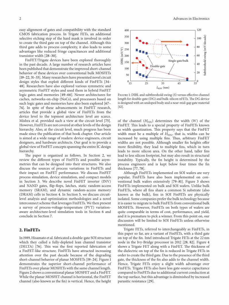
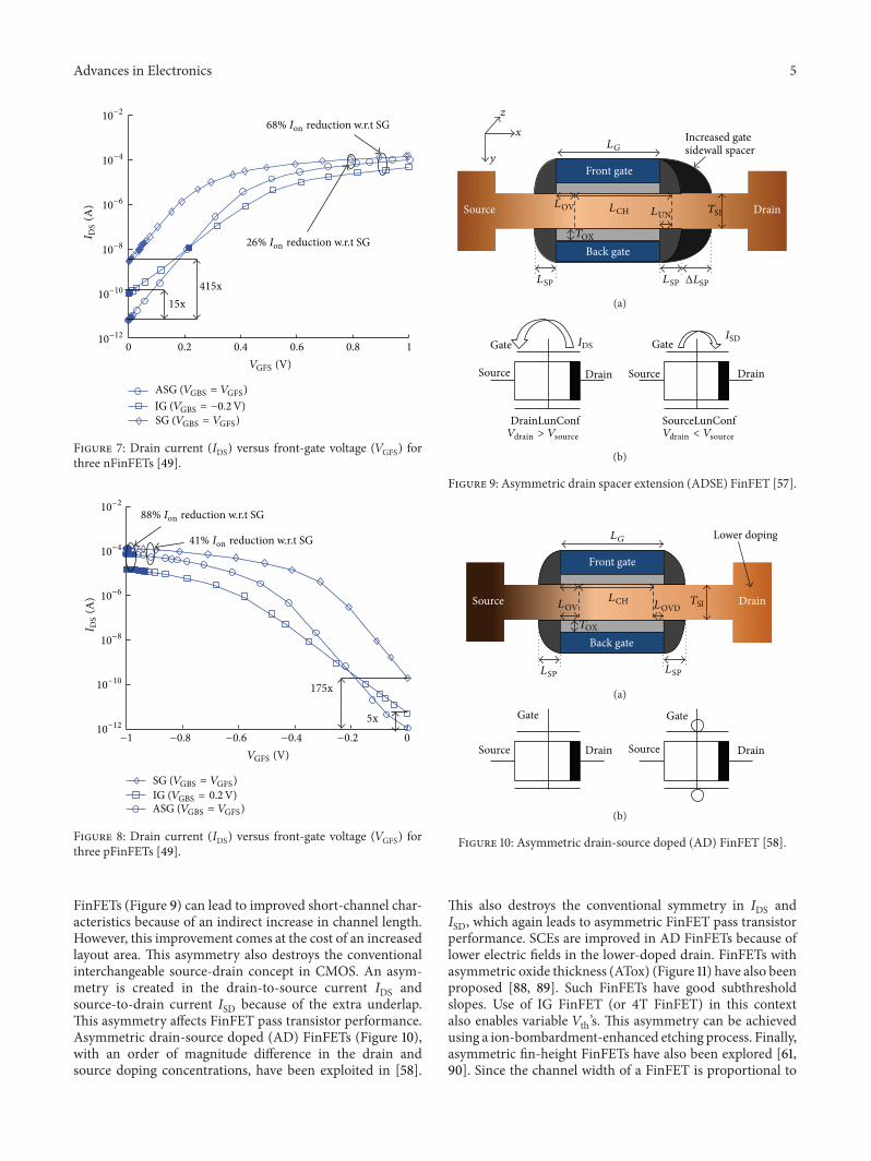
SG FinFETs can be further categorized based on asymme-tries in their device parameters. Normally, the workfunctions(Φ) of both the front and back gates of a FinFET are thesame.However, theworkfunctions can also bemade different.This leads to an asymmetric gate-workfunction SG FinFETor ASG FinFET (Figure 6) [86, 87]. ASG FinFETs can befabricated with selective doping of the two gate-stacks. Theyhave very promising short-channel characteristics and havetwo orders of magnitude lower 𝐼off compared to that ofan SG FinFET, with 𝐼on only somewhat lower than that ofan SG FinFET [49]. Figures 7 and 8 show comparisons ofthe drain current 𝐼DS versus front-gate voltage 𝑉GFS curvesfor SG, IG, and ASG nFinFETs and pFinFETs, respectively,demonstrating the advantages of ASG FinFETs.
Apart from gate-workfunction asymmetry, other asym-metries have also been explored in FinFETs. Goel et al.[57] show that asymmetric drain-spacer-extended (ADSE)
4 Advances in Electronics
Source
Drain
Gate 1
Gate 2
Dielectric thicknessof third gate
(a)
Source
Drain
Gate 3
Gate 1
Gate 2
Dielectric thicknessof third gate
(b)
Figure 4: Structural comparison between (a) FinFET and (b) Trigate FET.
Source
Drain
Gate 1
Gate 2
Gate dielectric
(a)
Source
Drain
Gate 1Gate 2
Gate dielectric
(b)
Figure 5: Structural comparison between (a) SG and (b) IG FinFET.
Source
Drain
Gate 1
Gate 2
Gate dielectric
(a)
Source
Drain
Gate 1
Gate 2
Gate dielectric
(b)
Figure 6: Structural comparison between (a) SG and (b) ASG FinFET; shaded gate implies different workfunctions.
Figure 7: Drain current (𝐼DS) versus front-gate voltage (𝑉GFS) forthree nFinFETs [49].
88% Ion reduction w.r.t SG
I DS
(A)
10−2
10−4
10−6
10−8
10−10
10−12
41% Ion reduction w.r.t SG
VGFS (V)
175x
5x
IG (VGBS = 0.2V)ASG (VGBS = VGFS)
SG (VGBS = VGFS)
−1 −0.8 −0.6 −0.4 −0.2 0
Figure 8: Drain current (𝐼DS) versus front-gate voltage (𝑉GFS) forthree pFinFETs [49].
FinFETs (Figure 9) can lead to improved short-channel char-acteristics because of an indirect increase in channel length.However, this improvement comes at the cost of an increasedlayout area. This asymmetry also destroys the conventionalinterchangeable source-drain concept in CMOS. An asym-metry is created in the drain-to-source current 𝐼DS andsource-to-drain current 𝐼SD because of the extra underlap.This asymmetry affects FinFET pass transistor performance.Asymmetric drain-source doped (AD) FinFETs (Figure 10),with an order of magnitude difference in the drain andsource doping concentrations, have been exploited in [58].
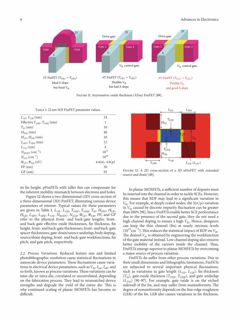
This also destroys the conventional symmetry in 𝐼DS and𝐼SD, which again leads to asymmetric FinFET pass transistorperformance. SCEs are improved in AD FinFETs because oflower electric fields in the lower-doped drain. FinFETs withasymmetric oxide thickness (ATox) (Figure 11) have also beenproposed [88, 89]. Such FinFETs have good subthresholdslopes. Use of IG FinFET (or 4T FinFET) in this contextalso enables variable 𝑉th’s. This asymmetry can be achievedusing a ion-bombardment-enhanced etching process. Finally,asymmetric fin-height FinFETs have also been explored [61,90]. Since the channel width of a FinFET is proportional to
its fin height, pFinFETs with taller fins can compensate forthe inherent mobility mismatch between electrons and holes.
Figure 12 shows a two-dimensional (2D) cross-section ofa three-dimensional (3D) FinFET, illustrating various deviceparameters of interest. Typical values for these parametersare given in Table 1. 𝐿GF, 𝐿GB, 𝑇OXF, 𝑇OXB, 𝑇SI, 𝐻FIN, 𝐻GF,𝐻GB, 𝐿SPF, 𝐿SPB, 𝐿UN, 𝑁BODY, 𝑁𝑆/𝐷, ΦGF, ΦGB, FP, and GPrefer to the physical front- and back-gate lengths, front-and back-gate effective oxide thicknesses, fin thickness, finheight, front- and back-gate thicknesses, front- and back-gatespacer thicknesses, gate-drain/source underlap, body doping,source/drain doping, front- and back-gate workfunctions, finpitch, and gate pitch, respectively.
2.2. Process Variations. Reduced feature size and limitedphotolithographic resolution cause statistical fluctuations innanoscale device parameters. These fluctuations cause varia-tions in electrical device parameters, such as𝑉th, 𝐼on, 𝐼off , andso forth, known as process variations.These variations can beinter-die or intra-die, correlated or uncorrelated, dependingon the fabrication process. They lead to mismatched devicestrengths and degrade the yield of the entire die. This iswhy continued scaling of planar MOSFETs has become sodifficult.
LGF LSPF
LSPBLGB
LUN (LOV)
TOXFHGF
TSI
TOXBHGB
Figure 12: A 2D cross-section of a 3D nFinFET with extendedsource and drain [49].
In planar MOSFETs, a sufficient number of dopants mustbe inserted into the channel in order to tackle SCEs. However,this means that RDF may lead to a significant variation in𝑉th. For example, at deeply scaled nodes, the 3(𝜎/𝜇) variationin 𝑉th caused by discrete impurity fluctuation can be greaterthan 100% [91]. Since FinFETs enable better SCEperformancedue to the presence of the second gate, they do not need ahigh channel doping to ensure a high 𝑉th. Hence, designerscan keep the thin channel (fin) at nearly intrinsic levels(1015cm−3).This reduces the statistical impact of RDF on𝑉th.The desired 𝑉th is obtained by engineering the workfunctionof the gate material instead. Low channel doping also ensuresbetter mobility of the carriers inside the channel. Thus,FinFETs emerge superior to planar MOSFETs by overcominga major source of process variation.
FinFETs do suffer from other process variations. Due totheir small dimensions and lithographic limitations, FinFETsare subjected to several important physical fluctuations,such as variations in gate length (𝐿GF, 𝐿GB), fin-thickness(𝑇SI), gate-oxide thickness (𝑇OXF, 𝑇OXB), and gate underlap(𝐿UN) [91–97]. For example, gate oxide is on the etchedsidewall of the fin, and may suffer from nonuniformity. Thedegree of nonuniformity depends on the line-edge roughness(LER) of the fin. LER also causes variations in fin thickness.
Advances in Electronics 7Pr
obab
ility
of o
ccur
renc
e
0.25
0.2
0.15
0.1
0.05
0−9.4 −9.3 −9.1−9.2 −9.0 −8.9 −8.8 −8.7 −8.6
LUN
LUN
TOX
TOX
LG
LG
TSI
TSI
Log10(Ioff/1A)
Figure 13: Distribution of leakage current (𝐼off ) for different processparameters, each varying independently [94].
10−7
10−8
10−9
10−10
10−11
10−12
I off
(A)
280 300 320 340 360 380 400
Temperature (K)
640x
104x
8x
18x
ASGSGIG (VGBS = −0.2V)
Figure 14: 𝐼off versus temperature for three nFinFETs [49].
Figure 13 shows the impact of parametric variations on thesubthreshold current (𝐼off ) of an nFinFET. Xiong and Bokorhave studied the sensitivity of electrical parameters to variousphysical variations in devices designed with a nearly intrinsicchannel [91].
Choi et al. have studied temperature variations in FinFETcircuits under above-mentioned physical parameters varia-tions [98]. They showed that even under moderate processvariations (3(𝜎/𝜇) = 10%) in gate length (𝐿GF, 𝐿GB) andbody thickness (𝑇SI), thermal runaway is possible in morethan 15% of ICs when primary input switching activity is0.4. The effect of temperature variation is more severe in
Freq
uenc
y
25
20
15
10
5
0−13 −12 −11 −10 −9 −8 −7 −6
ASG
IGSG
Log10(Ioff/1A)
Figure 15: Distributions of 𝐼off under process variations for threenFinFETs [49].
SOI FinFETs because the oxide layer under the fin has poorthermal conductivity. Hence, heat generated in the fin cannotdissipate easily in SOI FinFETs. Bhoj and Jha have evaluatedSG, IG, and ASG FinFETs under temperature variation andfound that even though 𝐼off degrades for all three FinFETsat a higher temperature, ASG FinFETs still remain the bestand retain a 100× advantage over SG FinFETs, as shown inFigure 14 [49].They also showed the distribution of 𝐼off underprocess variations for the three FinFETs (Figure 15).
3. FinFET Device Characterization
In this section, we discuss various ways of characterizing Fin-FET devices through simulation. Process simulation followedby device simulation constitutes a technology computer-aided design (TCAD) characterization flow of nanoscaledevices, such as FinFETs. Compact models, on the otherhand, have been another very popular way of characterizingCMOS devices for decades.
3.1. Process Simulation. Real devices undergo several process-ing steps.The functionality and performance of the fabricateddevices depend on how optimized the process flow is. TCADprocess simulation is, therefore, an important step in FinFETdevice optimization. Process simulation is followed by devicesimulation.These two simulation steps form an optimizationloop in which small changes in the process flow (e.g., time,temperature, doses, etc.) can lead to desirable electricalcharacteristics of the device. Thus, process simulation helpsdevice engineers explore the parameter space of the process,obviating the need for actual device fabrication. Although 3Dprocess simulation is computationally very expensive, it notonly gives good insights into device physics but also providesa cost-effective pre-fabrication process optimization flow.
The Sentaurus process and device simulator from Syn-opsys is a widely used tool for process simulation [99].Its 3D process simulation framework is compatible withthe mainstream 2D TCAD framework TSUPREM4/MEDICI
8 Advances in Electronics
(also from Synopsys). The 2D framework has been used bydesigners over the past decade and has been well-calibratedwith advanced CMOS libraries. Nawaz et al. have imple-mented a complete FinFET process flow as a commercially-available process and device simulation environment [100].As in real devices, all important geometrical features, such ascorner roundings and 3D facets, have been implemented intheir setup.
Process simulations of large layouts that consist of multi-ple devices incur extremely high computational costs. A novellayout/process/device-independent TCADmethodology wasproposed in [54] in order to overcome the process simulationbarrier for accurate 3D TCAD structure synthesis. In it, Bhojet al. adopt an automated structure synthesis approach thatobviates the need for repetitive 3D process simulations fordifferent layouts. In this approach, process-simulated unitdevices are placed at the device locations in the layout,eliminating the need for process simulation of the entirelayout, thereby reducing computational costs significantly.This structure synthesis approach, followed by transportanalysis based capacitance extraction methodology, has beenshown to capture accurate parasitic capacitances in FinFETSRAMs and ring oscillators in a practical timeframe [54, 55,63, 66]. Accurate extraction of parasitic capacitances has ledto a comprehensive evaluation of transient metrics of variousFinFET SRAM bitcells [55].
3.2. Device Simulation. After process simulation generatesa meshed device structure, device simulation is performedon the structure by invoking appropriate transport models.The conventional drift-diffusion transport model is not ade-quate for capturing SCEs in nanometer MOSFETs and Fin-FETs. The hydrodynamic model, with quantum corrections(such as density gradient models), has been popular amongresearchers for FinFET device simulation [101]. Other moreaccurate models, such as Green’s function based solutionto Boltzmann’s transport equation, impose a drastic com-putational burden [101]. In order to simulate circuits withmultiple devices, Sentaurus device (Synopsys) allows mixed-mode device simulation. Here, individual FinFET devices areconnected externally using wires or other circuit elements toform a netlist and coupled transport equations are solved onthe entire netlist. This feature enables device engineers to seehow the device behaves when used in a circuit.
3.3. Compact Models. Physics based compact models ofFinFETs have been a very useful tool for designers. Berke-ley short-channel IGFET model (BSIM) and University ofFlorida double-gate model (UFDG) for SOI multigate MOS-FETs and FinFETs were built using TCAD and calibratedusing fabricated hardware [102–105]. These models are com-patible with commercial circuit simulators, such as simu-lation program with integrated circuit emphasis (SPICE).Hence, large netlists can be simulated with these models aslong as the solution space is within their range. However,device simulation precedes derivation of compactmodels andis more accurate. Thus, all results presented in this article arebased on mixed-mode device simulations.
(a) (b) (c) (d)
ΦGF = ΦGB = 4.4 eV ΦGF = ΦGB = 4.8 eV
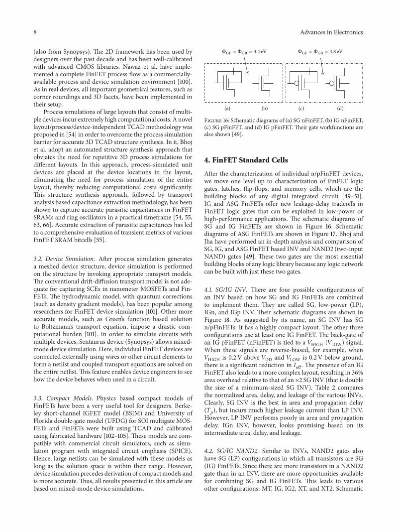
Figure 16: Schematic diagrams of (a) SG nFinFET, (b) IG nFinFET,(c) SG pFinFET, and (d) IG pFinFET. Their gate workfunctions arealso shown [49].
4. FinFET Standard Cells
After the characterization of individual n/pFinFET devices,we move one level up to characterization of FinFET logicgates, latches, flip-flops, and memory cells, which are thebuilding blocks of any digital integrated circuit [49–51].IG and ASG FinFETs offer new leakage-delay tradeoffs inFinFET logic gates that can be exploited in low-power orhigh-performance applications. The schematic diagrams ofSG and IG FinFETs are shown in Figure 16. Schematicdiagrams of ASG FinFETs are shown in Figure 17. Bhoj andJha have performed an in-depth analysis and comparison ofSG, IG, and ASG FinFET based INV and NAND2 (two-inputNAND) gates [49]. These two gates are the most essentialbuilding blocks of any logic library because any logic networkcan be built with just these two gates.
4.1. SG/IG INV. There are four possible configurations ofan INV based on how SG and IG FinFETs are combinedto implement them. They are called SG, low-power (LP),IGn, and IGp INV. Their schematic diagrams are shown inFigure 18. As suggested by its name, an SG INV has SGn/pFinFETs. It has a highly compact layout. The other threeconfigurations use at least one IG FinFET. The back-gate ofan IG pFinFET (nFinFET) is tied to a 𝑉HIGH (𝑉LOW) signal.When these signals are reverse-biased, for example, when𝑉HIGH is 0.2 V above 𝑉DD and 𝑉LOW is 0.2 V below ground,there is a significant reduction in 𝐼off . The presence of an IGFinFET also leads to a more complex layout, resulting in 36%area overhead relative to that of an ×2 SG INV (that is doublethe size of a minimum-sized SG INV). Table 2 comparesthe normalized area, delay, and leakage of the various INVs.Clearly, SG INV is the best in area and propagation delay(𝑇𝑝), but incurs much higher leakage current than LP INV.
However, LP INV performs poorly in area and propagationdelay. IGn INV, however, looks promising based on itsintermediate area, delay, and leakage.
4.2. SG/IG NAND2. Similar to INVs, NAND2 gates alsohave SG (LP) configurations in which all transistors are SG(IG) FinFETs. Since there are more transistors in a NAND2gate than in an INV, there are more opportunities availablefor combining SG and IG FinFETs. This leads to variousother configurations: MT, IG, IG2, XT, and XT2. Schematic
Advances in Electronics 9
ΦGB = 4.4 eV
ΦGF = 4.8 eV
(a)
ΦGB = 4.4 eV
ΦGF = 4.8 eV
(b)
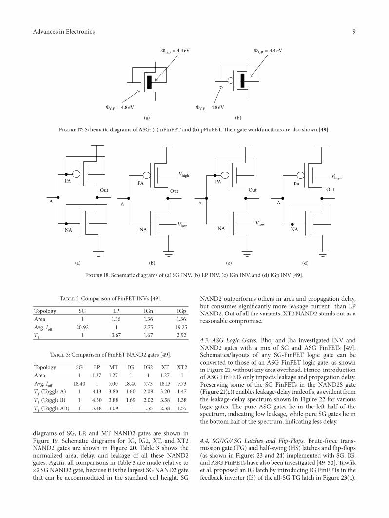
Figure 17: Schematic diagrams of ASG: (a) nFinFET and (b) pFinFET. Their gate workfunctions are also shown [49].
A
PA
NA
Out
(a)
A
PA
NA
Out
Vhigh
Vlow
(b)
A
PA
NA
Out
Vlow
(c)
A
PA
NA
Out
Vhigh
(d)
Figure 18: Schematic diagrams of (a) SG INV, (b) LP INV, (c) IGn INV, and (d) IGp INV [49].
diagrams of SG, LP, and MT NAND2 gates are shown inFigure 19. Schematic diagrams for IG, IG2, XT, and XT2NAND2 gates are shown in Figure 20. Table 3 shows thenormalized area, delay, and leakage of all these NAND2gates. Again, all comparisons in Table 3 are made relative to×2 SG NAND2 gate, because it is the largest SG NAND2 gatethat can be accommodated in the standard cell height. SG
NAND2 outperforms others in area and propagation delay,but consumes significantly more leakage current than LPNAND2. Out of all the variants, XT2 NAND2 stands out as areasonable compromise.
4.3. ASG Logic Gates. Bhoj and Jha investigated INV andNAND2 gates with a mix of SG and ASG FinFETs [49].Schematics/layouts of any SG-FinFET logic gate can beconverted to those of an ASG-FinFET logic gate, as shownin Figure 21, without any area overhead. Hence, introductionof ASG FinFETs only impacts leakage and propagation delay.Preserving some of the SG FinFETs in the NAND2S gate(Figure 21(c)) enables leakage-delay tradeoffs, as evident fromthe leakage-delay spectrum shown in Figure 22 for variouslogic gates. The pure ASG gates lie in the left half of thespectrum, indicating low leakage, while pure SG gates lie inthe bottom half of the spectrum, indicating less delay.
4.4. SG/IG/ASG Latches and Flip-Flops. Brute-force trans-mission gate (TG) and half-swing (HS) latches and flip-flops(as shown in Figures 23 and 24) implemented with SG, IG,andASGFinFETs have also been investigated [49, 50]. Tawfiket al. proposed an IG latch by introducing IG FinFETs in thefeedback inverter (I3) of the all-SG TG latch in Figure 23(a).
10 Advances in Electronics
AB
Out
PB
PA
NA
NB
(a)
AB
Out
Vhigh
Vlow
PB
PA
NA
NB
(b)
ABOut
Vhigh
Vlow
PB
PA
NA
NB
(c)
Figure 19: Schematic diagrams of NAND2 gates: (a) SG, (b) LP, and (c) MT [49].
AB
Out
PA
NA
NB
(a)
AB
Out
Vlow
PA
NA
NB
(b)
AB
Out
VhighPB PA
NA
NB
(c)
ABOut
Vlow
PB PA
NA
NB
(d)
Figure 20: Schematic diagrams of NAND2 gates: (a) IG, (b) IG2, (c) XT, and (d) XT2 [49].
With appropriate reverse-biasing of the back gates, the IGFinFETs in I3 aremadeweaker compared to the drive inverter(I1). As a result, the drive inverter need not be oversized,as conventionally done, ensuring a safe write operation atthe same time. At nominal process corners, the IG latchleads to 33% less leakage power and 20% less area comparedto the conventional SG latch with almost no degradationin propagation delay and setup time. Similar power and
area improvements are obtained for IG flip-flops relative toTG flip-flops (Figure 24(a)). Bhoj and Jha introduced ASGFinFETs in the TG and HS latches and observed similartradeoffs. Introducing ASG FinFETs in all the latch inverters(I1, I2, and I3) results in a minimum-leakage and maximum-delay configuration. Introducing ASG FinFETs in only I3leads to a configuration similar to the IG latch. The newconfiguration reduces leakage power by approximately 50%,
Advances in Electronics 11
A Out
(a)
A B
Out
(b)
A B
Out
(c)
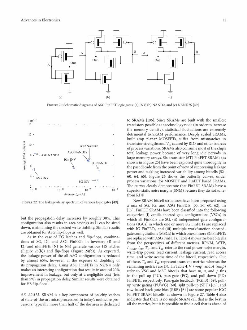
Figure 21: Schematic diagrams of ASG FinFET logic gates: (a) INV, (b) NAND2, and (c) NAND2S [49].
×10−12
14
12
10
8
6
4
2
Aver
age F
O4
delay
(s)
10−11 10−10 10−9 10−8
Average Ioff (A)
ASG NAND2
XT2 NAND2
ASG NAND2S
IGn INV
ASG INV
SG NAND2
SG INV
Figure 22: The leakage-delay spectrum of various logic gates [49].
but the propagation delay increases by roughly 30%. Thisconfiguration also results in area savings as I1 can be sizeddown, maintaining the desired write stability. Similar resultsare obtained for ASG flip-flops as well.
As in the case of TG latches and flip-flops, combina-tions of SG, IG, and ASG FinFETs in inverters (I1 andI2) and nFinFETs (N1 to N4) generate various HS latches(Figure 23(b)) and flip-flops (Figure 24(b)). As expected,the leakage power of the all-ASG configuration is reducedby almost 65%, however, at the expense of doubling ofits propagation delay. Using ASG FinFETs in N2/N4 onlymakes an interesting configuration that results in around 20%improvement in leakage, but only at a negligible cost (lessthan 5%) in propagation delay. Similar results were obtainedfor HS flip-flops.
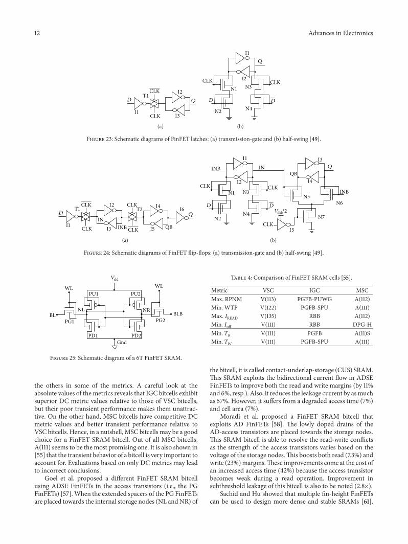
4.5. SRAM. SRAM is a key component of on-chip cachesof state-of-the-art microprocessors. In today’s multicore pro-cessors, typically more than half of the die area is dedicated
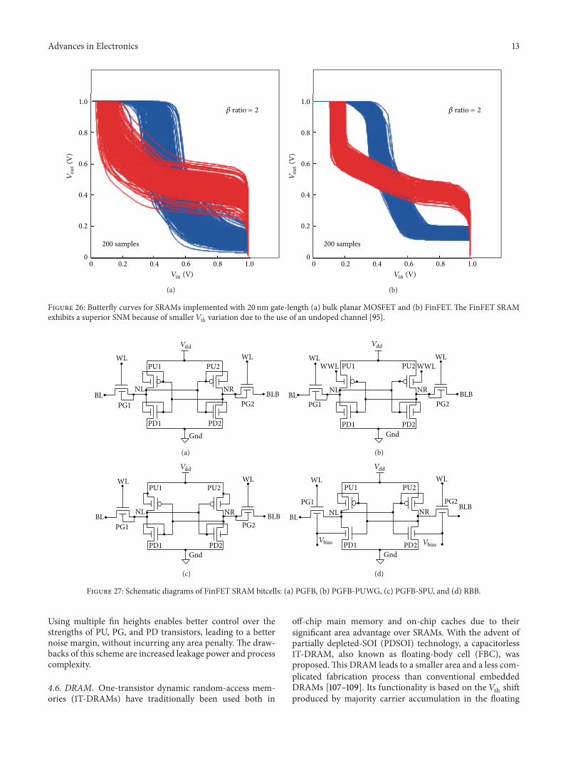
to SRAMs [106]. Since SRAMs are built with the smallesttransistors possible at a technology node (in order to increasethe memory density), statistical fluctuations are extremelydetrimental to SRAM performance. Deeply scaled SRAMs,built atop planar MOSFETs, suffer from mismatches intransistor strengths and𝑉th caused by RDF and other sourcesof process variations. SRAMs also consumemost of the chip’stotal leakage power because of very long idle periods inlarge memory arrays. Six-transistor (6T) FinFET SRAMs (asshown in Figure 25) have been explored quite thoroughly inthe past decade from the point of view of suppressing leakagepower and tackling increased variability among bitcells [52–60, 64, 65]. Figure 26 shows the butterfly curves, underprocess variations, for MOSFET and FinFET based SRAMs.The curves clearly demonstrate that FinFET SRAMs have asuperior static noisemargin (SNM)because they donot sufferfrom RDF.
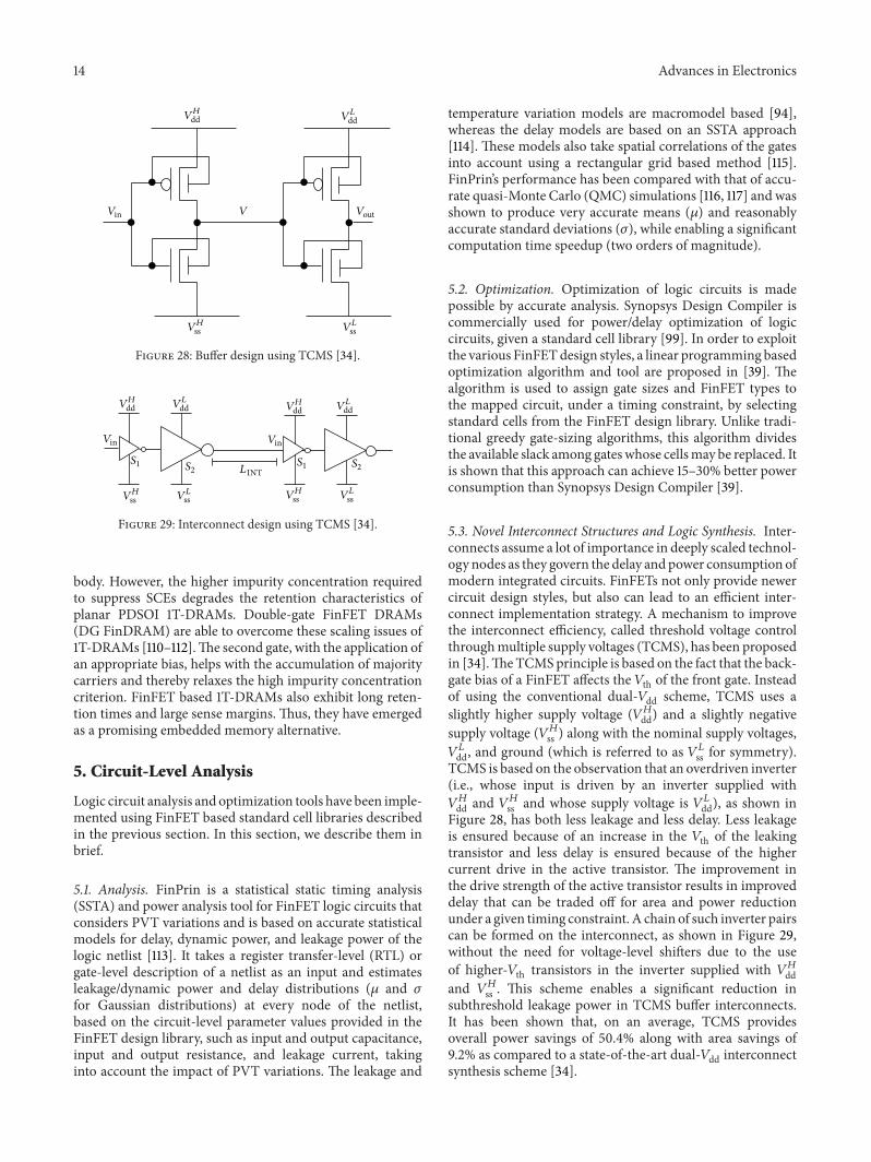
New SRAM bitcell structures have been proposed usinga mix of SG, IG, and ASG FinFETs [55, 56, 60, 62]. In[55], FinFET SRAMs have been classified into the followingcategories: (i) vanilla shorted-gate configurations (VSCs) inwhich all FinFETs are SG, (ii) independent-gate configura-tions (IGCs) in which one or more SG FinFETs are replacedwith IG FinFETs, and (iii) multiple workfunction shorted-gate configurations (MSCs) inwhich one ormore SGFinFETsare replacedwithASGFinFETs. Table 4 shows the best bitcellsfrom the perspectives of different metrics. RPNM, WTP,𝐼READ, 𝐼off , 𝑇𝑅, and 𝑇𝑊 refer to the read power noise margin,write-trip power, read current, leakage current, read accesstime, and write access time of the bitcell, respectively. Outof these, 𝑇
𝑅and 𝑇
𝑊represent transient metrics whereas the
remaining metrics are DC. In Table 4,𝑉 (𝑚𝑛𝑝) and𝐴 (𝑚𝑛𝑝)refer to VSC and MSC bitcells that have 𝑚, 𝑛, and 𝑝 finsin the pull-up (PU), pass-gate (PG), and pull-down (PD)FinFETs, respectively. Pass-gate feedback (PGFB) [59], pull-up write gating (PUWG) [60], split pull-up (SPU) [65], androw-based back-gate bias (RBB) [64] are some popular IGCFinFET SRAM bitcells, as shown in Figure 27. Table 4 alsoindicates that there is no single SRAM cell that is the best inall the metrics, but it is possible to find a cell that is ahead of
12 Advances in Electronics
D Q
CLK
CLKT1
I1
I2
I3
(a)
D
Q
CLK CLK
I1
I2
N1
N2
N3
N4
D
(b)
Figure 23: Schematic diagrams of FinFET latches: (a) transmission-gate and (b) half-swing [49].
D Q
CLK
CLKCLK
CLK
INQBINB
T1
I1
I2T2
I3
I4
I5
I6
(a)
D
Q
CLK CLK
CLK
INQB
INB
INB
I1
I2
I3
I4
I5
N1
N2
N3
N4
N5N6
N7Vdd/2
D
(b)
Figure 24: Schematic diagrams of FinFET flip-flops: (a) transmission-gate and (b) half-swing [49].
WL
BLPG1
NL
PU1
PD1
PU2
PD2
Gnd
NR
WL
PG2BLB
Vdd
Figure 25: Schematic diagram of a 6T FinFET SRAM.
the others in some of the metrics. A careful look at theabsolute values of the metrics reveals that IGC bitcells exhibitsuperior DC metric values relative to those of VSC bitcells,but their poor transient performance makes them unattrac-tive. On the other hand, MSC bitcells have competitive DCmetric values and better transient performance relative toVSC bitcells. Hence, in a nutshell, MSC bitcells may be a goodchoice for a FinFET SRAM bitcell. Out of all MSC bitcells,A(111) seems to be themost promising one. It is also shown in[55] that the transient behavior of a bitcell is very important toaccount for. Evaluations based on only DC metrics may leadto incorrect conclusions.
Goel et al. proposed a different FinFET SRAM bitcellusing ADSE FinFETs in the access transistors (i.e., the PGFinFETs) [57].When the extended spacers of the PG FinFETsare placed towards the internal storage nodes (NL andNR) of
the bitcell, it is called contact-underlap-storage (CUS) SRAM.This SRAM exploits the bidirectional current flow in ADSEFinFETs to improve both the read and write margins (by 11%and 6%, resp.). Also, it reduces the leakage current by asmuchas 57%. However, it suffers from a degraded access time (7%)and cell area (7%).
Moradi et al. proposed a FinFET SRAM bitcell thatexploits AD FinFETs [58]. The lowly doped drains of theAD-access transistors are placed towards the storage nodes.This SRAM bitcell is able to resolve the read-write conflictsas the strength of the access transistors varies based on thevoltage of the storage nodes.This boosts both read (7.3%) andwrite (23%)margins.These improvements come at the cost ofan increased access time (42%) because the access transistorbecomes weak during a read operation. Improvement insubthreshold leakage of this bitcell is also to be noted (2.8×).
Sachid and Hu showed that multiple fin-height FinFETscan be used to design more dense and stable SRAMs [61].
Advances in Electronics 13
1.0
0.8
0.6
0.4
0.2
0
Vou
t(V
)
0 0.2 0.4 0.6 0.8 1.0
Vin (V)
200 samples
𝛽 ratio = 2
(a)
1.0
0.8
0.6
0.4
0.2
0
Vou
t(V
)
0 0.2 0.4 0.6 0.8 1.0
Vin (V)
200 samples
𝛽 ratio = 2
(b)
Figure 26: Butterfly curves for SRAMs implemented with 20 nm gate-length (a) bulk planar MOSFET and (b) FinFET. The FinFET SRAMexhibits a superior SNM because of smaller 𝑉th variation due to the use of an undoped channel [95].
WL
BLPG1
NL
PU1
PD1
PU2
PD2
Gnd
NR
WL
PG2
BLB
Vdd
(a)
WLWWL WWL
WL
BLPG1
NL
PU1
PD1
PU2
PD2
Gnd
NR
PG2
BLB
Vdd
(b)
WL
BLPG1
NL
PU1
PD1
PU2
PD2
Gnd
NR
WL
PG2BLB
Vdd
(c)
BL NL
PU1 PU2
PD1 PD2
Gnd
NR
WL WL
PG1 PG2BLB
Vdd
Vbias Vbias
(d)
Figure 27: Schematic diagrams of FinFET SRAM bitcells: (a) PGFB, (b) PGFB-PUWG, (c) PGFB-SPU, and (d) RBB.
Using multiple fin heights enables better control over thestrengths of PU, PG, and PD transistors, leading to a betternoise margin, without incurring any area penalty. The draw-backs of this scheme are increased leakage power and processcomplexity.
4.6. DRAM. One-transistor dynamic random-access mem-ories (1T-DRAMs) have traditionally been used both in
off-chip main memory and on-chip caches due to theirsignificant area advantage over SRAMs. With the advent ofpartially depleted-SOI (PDSOI) technology, a capacitorless1T-DRAM, also known as floating-body cell (FBC), wasproposed.This DRAM leads to a smaller area and a less com-plicated fabrication process than conventional embeddedDRAMs [107–109]. Its functionality is based on the 𝑉th shiftproduced by majority carrier accumulation in the floating
14 Advances in Electronics
VHdd VL
dd
Vin V Vout
VHss VL
ss
Figure 28: Buffer design using TCMS [34].
VHdd VH
ddVLdd VL
dd
Vin Vin
VHss VH
ssVLss VL
ss
S1 S1S2 S2LINT
Figure 29: Interconnect design using TCMS [34].
body. However, the higher impurity concentration requiredto suppress SCEs degrades the retention characteristics ofplanar PDSOI 1T-DRAMs. Double-gate FinFET DRAMs(DG FinDRAM) are able to overcome these scaling issues of1T-DRAMs [110–112].The second gate, with the application ofan appropriate bias, helps with the accumulation of majoritycarriers and thereby relaxes the high impurity concentrationcriterion. FinFET based 1T-DRAMs also exhibit long reten-tion times and large sense margins. Thus, they have emergedas a promising embedded memory alternative.
5. Circuit-Level Analysis
Logic circuit analysis and optimization tools have been imple-mented using FinFET based standard cell libraries describedin the previous section. In this section, we describe them inbrief.
5.1. Analysis. FinPrin is a statistical static timing analysis(SSTA) and power analysis tool for FinFET logic circuits thatconsiders PVT variations and is based on accurate statisticalmodels for delay, dynamic power, and leakage power of thelogic netlist [113]. It takes a register transfer-level (RTL) orgate-level description of a netlist as an input and estimatesleakage/dynamic power and delay distributions (𝜇 and 𝜎for Gaussian distributions) at every node of the netlist,based on the circuit-level parameter values provided in theFinFET design library, such as input and output capacitance,input and output resistance, and leakage current, takinginto account the impact of PVT variations. The leakage and
temperature variation models are macromodel based [94],whereas the delay models are based on an SSTA approach[114]. These models also take spatial correlations of the gatesinto account using a rectangular grid based method [115].FinPrin’s performance has been compared with that of accu-rate quasi-Monte Carlo (QMC) simulations [116, 117] and wasshown to produce very accurate means (𝜇) and reasonablyaccurate standard deviations (𝜎), while enabling a significantcomputation time speedup (two orders of magnitude).
5.2. Optimization. Optimization of logic circuits is madepossible by accurate analysis. Synopsys Design Compiler iscommercially used for power/delay optimization of logiccircuits, given a standard cell library [99]. In order to exploitthe various FinFETdesign styles, a linear programming basedoptimization algorithm and tool are proposed in [39]. Thealgorithm is used to assign gate sizes and FinFET types tothe mapped circuit, under a timing constraint, by selectingstandard cells from the FinFET design library. Unlike tradi-tional greedy gate-sizing algorithms, this algorithm dividesthe available slack among gateswhose cellsmay be replaced. Itis shown that this approach can achieve 15–30% better powerconsumption than Synopsys Design Compiler [39].
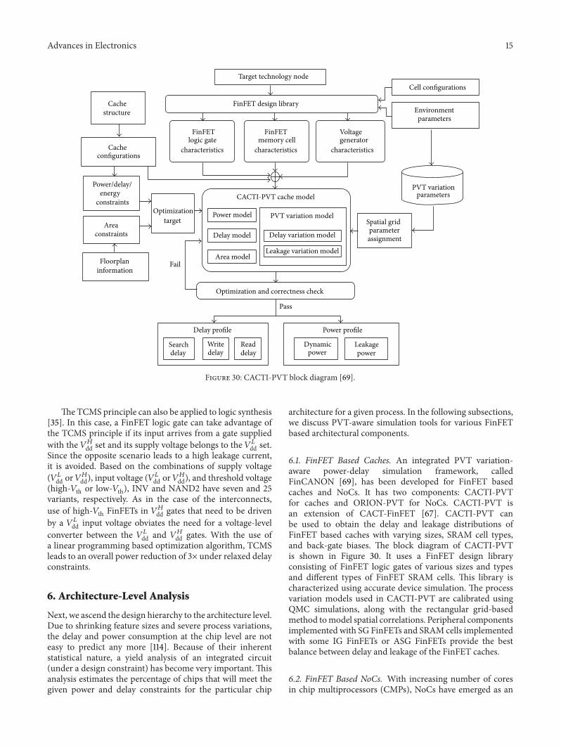
5.3. Novel Interconnect Structures and Logic Synthesis. Inter-connects assume a lot of importance in deeply scaled technol-ogy nodes as they govern the delay andpower consumption ofmodern integrated circuits. FinFETs not only provide newercircuit design styles, but also can lead to an efficient inter-connect implementation strategy. A mechanism to improvethe interconnect efficiency, called threshold voltage controlthroughmultiple supply voltages (TCMS), has been proposedin [34].TheTCMSprinciple is based on the fact that the back-gate bias of a FinFET affects the 𝑉th of the front gate. Insteadof using the conventional dual-𝑉dd scheme, TCMS uses aslightly higher supply voltage (𝑉𝐻dd) and a slightly negativesupply voltage (𝑉𝐻ss ) along with the nominal supply voltages,𝑉𝐿
dd, and ground (which is referred to as 𝑉𝐿ss for symmetry).TCMS is based on the observation that an overdriven inverter(i.e., whose input is driven by an inverter supplied with𝑉𝐻
dd and 𝑉𝐻ss and whose supply voltage is 𝑉𝐿dd), as shown inFigure 28, has both less leakage and less delay. Less leakageis ensured because of an increase in the 𝑉th of the leakingtransistor and less delay is ensured because of the highercurrent drive in the active transistor. The improvement inthe drive strength of the active transistor results in improveddelay that can be traded off for area and power reductionunder a given timing constraint. A chain of such inverter pairscan be formed on the interconnect, as shown in Figure 29,without the need for voltage-level shifters due to the useof higher-𝑉th transistors in the inverter supplied with 𝑉𝐻ddand 𝑉𝐻ss . This scheme enables a significant reduction insubthreshold leakage power in TCMS buffer interconnects.It has been shown that, on an average, TCMS providesoverall power savings of 50.4% along with area savings of9.2% as compared to a state-of-the-art dual-𝑉dd interconnectsynthesis scheme [34].
Advances in Electronics 15
Target technology node
FinFET design library
FinFETlogic gate
characteristics
FinFETmemory cell
characteristics
Voltagegenerator
characteristics
Cachestructure
Cacheconfigurations
Power/delay/energy
constraints
Areaconstraints
Floorplaninformation
Optimizationtarget
CACTI-PVT cache model
Power model
Delay model
Area model
PVT variation model
Delay variation model
Leakage variation model
Fail
Optimization and correctness check
Pass
Delay profile
Searchdelay
Writedelay
Readdelay
Power profile
Dynamicpower
Leakagepower
Cell configurations
Environmentparameters
PVT variationparameters
Spatial gridparameterassignment
Figure 30: CACTI-PVT block diagram [69].
The TCMS principle can also be applied to logic synthesis[35]. In this case, a FinFET logic gate can take advantage ofthe TCMS principle if its input arrives from a gate suppliedwith the 𝑉𝐻dd set and its supply voltage belongs to the 𝑉𝐿dd set.Since the opposite scenario leads to a high leakage current,it is avoided. Based on the combinations of supply voltage(𝑉𝐿dd or𝑉
𝐻
dd), input voltage (𝑉𝐿
dd or𝑉𝐻
dd), and threshold voltage(high-𝑉th or low-𝑉th), INV and NAND2 have seven and 25variants, respectively. As in the case of the interconnects,use of high-𝑉th FinFETs in 𝑉𝐻dd gates that need to be drivenby a 𝑉𝐿dd input voltage obviates the need for a voltage-levelconverter between the 𝑉𝐿dd and 𝑉𝐻dd gates. With the use ofa linear programming based optimization algorithm, TCMSleads to an overall power reduction of 3× under relaxed delayconstraints.
6. Architecture-Level Analysis
Next, we ascend the design hierarchy to the architecture level.Due to shrinking feature sizes and severe process variations,the delay and power consumption at the chip level are noteasy to predict any more [114]. Because of their inherentstatistical nature, a yield analysis of an integrated circuit(under a design constraint) has become very important. Thisanalysis estimates the percentage of chips that will meet thegiven power and delay constraints for the particular chip
architecture for a given process. In the following subsections,we discuss PVT-aware simulation tools for various FinFETbased architectural components.
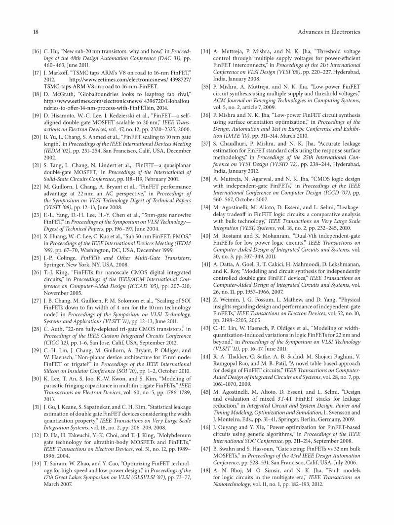
6.1. FinFET Based Caches. An integrated PVT variation-aware power-delay simulation framework, calledFinCANON [69], has been developed for FinFET basedcaches and NoCs. It has two components: CACTI-PVTfor caches and ORION-PVT for NoCs. CACTI-PVT isan extension of CACT-FinFET [67]. CACTI-PVT canbe used to obtain the delay and leakage distributions ofFinFET based caches with varying sizes, SRAM cell types,and back-gate biases. The block diagram of CACTI-PVTis shown in Figure 30. It uses a FinFET design libraryconsisting of FinFET logic gates of various sizes and typesand different types of FinFET SRAM cells. This library ischaracterized using accurate device simulation. The processvariation models used in CACTI-PVT are calibrated usingQMC simulations, along with the rectangular grid-basedmethod tomodel spatial correlations. Peripheral componentsimplemented with SG FinFETs and SRAM cells implementedwith some IG FinFETs or ASG FinFETs provide the bestbalance between delay and leakage of the FinFET caches.
6.2. FinFET Based NoCs. With increasing number of coresin chip multiprocessors (CMPs), NoCs have emerged as an
16 Advances in Electronics
Target technology node
FinFET design library
ORION-PVT
CACTI-PVT
Delay estimationmodel
Power estimationmodel
PVT variation model
SSTA delay model
Leakage macromodel
NOC component model
Routerconfiguration
Input buffermodel
Crossbarmodel
Arbitermodel
Clockmodel
Linkmodel
Routerdelay/power
profile
Clock/linkdelay/power
profile
Cellconfigurations
Environmentparameters
PVT variationparameters
Spatial gridparameterassignment
GEMSperformance
simulation
Network trafficprofile
Networkconfiguration
Figure 31: ORION-PVT block diagram [69].
effective communication mechanism among the cores. Fin-CANON also includes a performance/power simulation tool,called ORION-PVT, aimed at FinFET NoCs [69]. ORION-PVT, whose block diagram is shown in Figure 31, is anextension of ORION-FinFET [68]. Here, an SSTA techniqueand a macromodel based methodology are used to model thePVT variations in delay and leakage. It also provides a powerbreakdown of an on-chip router. Leakage power is found todominate the total power of the router at higher temperatures.
A FinFET based implementation of a variable-pipeline-stage router (VPSR) is proposed in [70]. VPSR enablesdynamic adjustment of the number of pipeline stages inthe router based on incoming network traffic. As a result,different flow control digits (flits) may traverse pipelinestages of varying lengths while passing through the router.This leads to enhanced router performance because VPSRadapts its throughput to the network traffic requirement atruntime. VPSR also enables significant savings in leakagepower through reverse-biasing (called adaptive back-gatebiasing) of the back gates of IG FinFETs in infrequentlyaccessed components of the router.
6.3. FinFET Based Multicore Processors. In the computerarchitecture domain, the trend has shifted in recent yearsfrom uniprocessors to CMPs and multicore systems in orderto serve the ever-increasing performance demand. Tools likeFinCANON have paved the way for a more powerful tool forcharacterizing multicore processors. McPAT-PVT is a PVT
variation-aware integrated power-delay simulation tool forFinFET based multicore processors [71]. Figure 32 shows theblock diagram of McPAT-PVT. It has two key components:processor model and yield analyzer. The processor modelcontains power/delay macromodels of various functionalunits (e.g., arithmetic-logic unit, floating-point unit, memorymanagement unit, etc.) of the processor core. The yieldanalyzer can predict the yield of a specified processor con-figuration under PVT variations. Figure 33 zooms into thecomponents of the processor model. The efficacy of thistool has been demonstrated on an alpha-like processor coreand multicore simulations based on Princeton ApplicationRepository for Shared-Memory Computer (PARSEC) bench-marks.
7. Conclusion
In this paper, we have explored the impact of FinFETsfrom the device to architecture level. We learnt about theshortcomings of planar MOSFETs in today’s deeply scaledtechnologies and the advantages of FinFETs as suitablereplacements for planar MOSFETs. We looked into FinFETdevice characteristics and evaluated tradeoffs among SG, IG,and ASG FinFETs, along with other FinFET asymmetries,such as drain-spacer extension, source/drain doping, gate-oxide thickness, and finheight.We learnt about the detrimen-tal impact of PVT variations on FinFET chip performance
and power. We surveyed techniques for characterizing Fin-FET devices and circuits and explored FinFET based logicgates, flip-flops, and memory cells. Finally, we also reviewedPVT variation-aware FinFET circuit- and architecture-levelsimulation tools.Weobserved leakage-delay tradeoffs that arepossible at each level of the design hierarchy. The availabilityof a plethora of FinFET styles opens up new design opportu-nities at each level, which we hope some of the readers will bewilling to explore.
Conflict of Interests
The authors declare that there is no conflict of interestsregarding the publication of this paper.
Acknowledgment
This work was supported by NSF under Grant nos. CCF-1217076 and CCF-1318603.
References
[1] K. J. Kuhn, “CMOS scaling for the 22nm node and beyond:Device physics and technology,” in Proceedings of the Interna-tional Symposium on VLSI Technology, Systems and Applications(VLSI-TSA ’11), pp. 1–2, April 2011.
[2] K. Roy, S.Mukhopadhyay, andH.Mahmoodi-Meimand, “Leak-age current mechanisms and leakage reduction techniques indeep-submicrometer CMOS circuits,” Proceedings of the IEEE,vol. 91, no. 2, pp. 305–327, 2003.
[3] D. J. Frank, R. H. Dennard, E. Nowak, P. M. Solomon, Y. Taur,and H.-S. P. Wong, “Device scaling limits of Si MOSFETs andtheir application dependencies,” Proceedings of the IEEE, vol. 89,no. 3, pp. 259–288, 2001.
[4] C. Hu, “Gate oxide scaling limits and projection,” in Proceedingsof the IEEE International Electron Devices Meeting, pp. 319–322,December 1996.
[5] Y.-C. Yeo, T.-J. King, and C. Hu, “MOSFET gate leakagemodeling and selection guide for alternative gate dielectricsbased on leakage considerations,” IEEE Transactions on ElectronDevices, vol. 50, no. 4, pp. 1027–1035, 2003.
[6] J. Chen, T. Y. Chan, I. C. Chen, P. K. Ko, and C. Hu, “Subbreak-down drain leakage current inMOSFET,” Electron device letters,vol. 8, no. 11, pp. 515–517, 1987.
[7] “International technology roadmap for semiconductors,” 2011,http://www.itrs.net.
[8] T. Skotnicki, J. A. Hutchby, T.-J. King, H.-S. P. Wong, and F.Boeuf, “The end of CMOS scaling: toward the introductionof new materials and structural changes to improve MOSFETperformance,” IEEE Circuits and Devices Magazine, vol. 21, no.1, pp. 16–26, 2005.
[9] H.-S. P. Wong, D. J. Franks, and P. M. Solomon, “Device designconsiderations for double-gate, ground-plane, and single-gatedultra-thin SOI MOSFET’s at the 25 nm channel length genera-tion,” in Proceedings of the IEEE International Electron DevicesMeeting (IEDM ’98), pp. 407–410, San Francisco, Calif, USA,December 1998.
[10] P. M. Solomon, K. W. Guarini, Y. Zhang et al., “Two gates arebetter than one,” IEEE Circuits and Devices Magazine, vol. 19,no. 1, pp. 48–62, 2003.
[11] K. Suzuki, T. Tanaka, Y. Tosaka,H.Horie, andY.Arimoto, “Scal-ing theory for double-gate SOI MOSFET’s,” IEEE Transactionson Electron Devices, vol. 40, no. 12, pp. 2326–2329, 1993.
[12] E. J. Nowak, I. Aller, T. Ludwig et al., “Turning silicon on itsedge [double gate CMOS/FinFET technology],” IEEE Circuitsand Devices Magazine, vol. 20, no. 1, pp. 20–31, 2004.
[13] R.-H. Yan, A. Ourmazd, and K. F. Lee, “Scaling the Si MOSFET:from bulk to SOI to bulk,” IEEE Transactions on ElectronDevices, vol. 39, no. 7, pp. 1704–1710, 1992.
[14] Y.-K. Choi, K. Asano, N. Lindert et al., “Ultrathin-body SOIMOSFET for deep-sub-tenth micron era,” IEEE Electron DeviceLetters, vol. 21, no. 5, pp. 254–255, 2000.
[15] B. Doris, K. Cheng, A. Khakifirooz, Q. Liu, and M. Vinet,“Device design considerations for next generation CMOS tech-nology: planar FDSOI and FinFET (Invited),” in Proceedings ofthe International Symposium on VLSI Technology, Systems, andApplications (VLSI-TSA ’13), pp. 1–2, April 2013.
18 Advances in Electronics
[16] C. Hu, “New sub-20 nm transistors: why and how,” in Proceed-ings of the 48th Design Automation Conference (DAC ’11), pp.460–463, June 2011.
[17] J. Markoff, “TSMC taps ARM's V8 on road to 16-nm FinFET,”2012, http://www.eetimes.com/electronicsnews/ 4398727/TSMC-taps-ARM-V8-in-road to-16-nm-FinFET.
[18] D. McGrath, “Globalfoundries looks to leapfrog fab rival,”http://www.eetimes.com/electronicsnews/ 4396720/Globalfoundries-to-offer-14-nm-process-with-FinFETsin, 2014.
[19] D. Hisamoto, W.-C. Lee, J. Kedzierski et al., “FinFET—a self-aligned double-gate MOSFET scalable to 20 nm,” IEEE Trans-actions on Electron Devices, vol. 47, no. 12, pp. 2320–2325, 2000.
[20] B. Yu, L. Chang, S. Ahmed et al., “FinFET scaling to 10 nm gatelength,” in Proceedings of the IEEE International DevicesMeeting(IEDM '02), pp. 251–254, San Francisco, Calif, USA, December2002.
[21] S. Tang, L. Chang, N. Lindert et al., “FinFET—a quasiplanardouble-gate MOSFET,” in Proceedings of the International ofSolid-State Circuits Conference, pp. 118–119, February 2001.
[22] M. Guillorn, J. Chang, A. Bryant et al., “FinFET performanceadvantage at 22 nm: an AC perspective,” in Proceedings ofthe Symposium on VLSI Technology Digest of Technical Papers(VLSIT ’08), pp. 12–13, June 2008.
[23] F.-L. Yang, D.-H. Lee, H.-Y. Chen et al., “5nm-gate nanowireFinFET,” in Proceedings of the Symposium on VLSI Technology—Digest of Technical Papers, pp. 196–197, June 2004.
[24] X.Huang,W.-C. Lee, C. Kuo et al., “Sub 50-nmFinFET: PMOS,”in Proceedings of the IEEE International Devices Meeting (IEDM'99), pp. 67–70, Washington, DC, USA, December 1999.
[25] J.-P. Colinge, FinFETs and Other Multi-Gate Transistors,Springer, New York, NY, USA, 2008.
[26] T.-J. King, “FinFETs for nanoscale CMOS digital integratedcircuits,” in Proceedings of the IEEE/ACM International Con-ference on Computer-Aided Design (ICCAD ’05), pp. 207–210,November 2005.
[27] J. B. Chang, M. Guillorn, P. M. Solomon et al., “Scaling of SOIFinFETs down to fin width of 4 nm for the 10 nm technologynode,” in Proceedings of the Symposium on VLSI Technology,Systems and Applications (VLSIT ’11), pp. 12–13, June 2011.
[28] C. Auth, “22-nm fully-depleted tri-gate CMOS transistors,” inProceedings of the IEEE Custom Integrated Circuits Conference(CICC '12), pp. 1–6, San Jose, Calif, USA, September 2012.
[29] C.-H. Lin, J. Chang, M. Guillorn, A. Bryant, P. Oldiges, andW. Haensch, “Non-planar device architecture for 15 nm node:FinFET or trigate?” in Proceedings of the IEEE InternationalSilicon on Insulator Conference (SOI ’10), pp. 1–2, October 2010.
[30] K. Lee, T. An, S. Joo, K.-W. Kwon, and S. Kim, “Modeling ofparasitic fringing capacitance inmultifin trigate FinFETs,” IEEETransactions on Electron Devices, vol. 60, no. 5, pp. 1786–1789,2013.
[31] J. Gu, J. Keane, S. Sapatnekar, and C. H. Kim, “Statistical leakageestimation of double gate FinFET devices considering the widthquantization property,” IEEE Transactions on Very Large ScaleIntegration Systems, vol. 16, no. 2, pp. 206–209, 2008.
[32] D. Ha, H. Takeuchi, Y.-K. Choi, and T.-J. King, “Molybdenumgate technology for ultrathin-body MOSFETs and FinFETs,”IEEE Transactions on Electron Devices, vol. 51, no. 12, pp. 1989–1996, 2004.
[33] T. Sairam, W. Zhao, and Y. Cao, “Optimizing FinFET technol-ogy for high-speed and low-power design,” in Proceedings of the17th Great Lakes Symposium on VLSI (GLSVLSI ’07), pp. 73–77,March 2007.
[34] A. Muttreja, P. Mishra, and N. K. Jha, “Threshold voltagecontrol through multiple supply voltages for power-efficientFinFET interconnects,” in Proceedings of the 21st InternationalConference on VLSI Design (VLSI '08), pp. 220–227, Hyderabad,India, January 2008.
[35] P. Mishra, A. Muttreja, and N. K. Jha, “Low-power FinFETcircuit synthesis using multiple supply and threshold voltages,”ACM Journal on Emerging Technologies in Computing Systems,vol. 5, no. 2, article 7, 2009.
[36] P. Mishra and N. K. Jha, “Low-power FinFET circuit synthesisusing surface orientation optimization,” in Proceedings of theDesign, Automation and Test in Europe Conference and Exhibi-tion (DATE ’10), pp. 311–314, March 2010.
[37] S. Chaudhuri, P. Mishra, and N. K. Jha, “Accurate leakageestimation for FinFET standard cells using the response surfacemethodology,” in Proceedings of the 25th International Con-ference on VLSI Design (VLSID '12), pp. 238–244, Hyderabad,India, January 2012.
[38] A. Muttreja, N. Agarwal, and N. K. Jha, “CMOS logic designwith independent-gate FinFETs,” in Proceedings of the IEEEInternational Conference on Computer Design (ICCD ’07), pp.560–567, October 2007.
[39] M. Agostinelli, M. Alioto, D. Esseni, and L. Selmi, “Leakage-delay tradeoff in FinFET logic circuits: a comparative analysiswith bulk technology,” IEEE Transactions on Very Large ScaleIntegration (VLSI) Systems, vol. 18, no. 2, pp. 232–245, 2010.
[40] M. Rostami and K. Mohanram, “Dual-Vth independent-gateFinFETs for low power logic circuits,” IEEE Transactions onComputer-Aided Design of Integrated Circuits and Systems, vol.30, no. 3, pp. 337–349, 2011.
[41] A. Datta, A. Goel, R. T. Cakici, H. Mahmoodi, D. Lekshmanan,and K. Roy, “Modeling and circuit synthesis for independentlycontrolled double gate FinFET devices,” IEEE Transactions onComputer-Aided Design of Integrated Circuits and Systems, vol.26, no. 11, pp. 1957–1966, 2007.
[42] Z. Weimin, J. G. Fossum, L. Mathew, and D. Yang, “Physicalinsights regarding design and performance of independent-gateFinFETs,” IEEE Transactions on Electron Devices, vol. 52, no. 10,pp. 2198–2205, 2005.
[43] C.-H. Lin, W. Haensch, P. Oldiges et al., “Modeling of width-quantization-induced variations in logic FinFETs for 22 nm andbeyond,” in Proceedings of the Symposium on VLSI Technology(VLSIT ’11), pp. 16–17, June 2011.
[44] R. A. Thakker, C. Sathe, A. B. Sachid, M. Shojaei Baghini, V.Ramgopal Rao, and M. B. Patil, “A novel table-based approachfor design of FinFET circuits,” IEEE Transactions on Computer-AidedDesign of Integrated Circuits and Systems, vol. 28, no. 7, pp.1061–1070, 2009.
[45] M. Agostinelli, M. Alioto, D. Esseni, and L. Selmi, “Designand evaluation of mixed 3T-4T FinFET stacks for leakagereduction,” in Integrated Circuit and System Design. Power andTimingModeling, Optimization and Simulation, L. Svensson andJ. Monteiro, Eds., pp. 31–41, Springer, Berlin, Germany, 2009.
[46] J. Ouyang and Y. Xie, “Power optimization for FinFET-basedcircuits using genetic algorithms,” in Proceedings of the IEEEInternational SOC Conference, pp. 211–214, September 2008.
[47] B. Swahn and S. Hassoun, “Gate sizing: FinFETs vs 32 nm bulkMOSFETs,” in Proceedings of the 43rd IEEE Design AutomationConference, pp. 528–531, San Francisco, Calif, USA, July 2006.
[48] A. N. Bhoj, M. O. Simsir, and N. K. Jha, “Fault modelsfor logic circuits in the multigate era,” IEEE Transactions onNanotechnology, vol. 11, no. 1, pp. 182–193, 2012.
Advances in Electronics 19
[49] A. N. Bhoj and N. K. Jha, “Design of logic gates and flip-flopsin high-performance FinFET technology,” IEEETransactions onVery Large Scale Integration (VLSI) Systems, vol. 21, no. 11, pp.1975–1988, 2013.
[50] S. A. Tawfik and V. Kursun, “Characterization of new staticindependent-gate-biased FinFET latches and flip-flops underprocess variations,” in Proceedings of the 9th InternationalSymposium on Quality Electronic Design (ISQED ’08), pp. 311–316, San Jose, Calif, USA, March 2008.
[51] S. A. Tawfik and V. Kursun, “Low-power and compact sequen-tial circuits with independent-gate FinFETs,” IEEE Transactionson Electron Devices, vol. 55, no. 1, pp. 60–70, 2008.
[52] A. Bansal, S. Mukhopadhyay, and K. Roy, “Device-optimizationtechnique for robust and low-power FinFET SRAM design inNanoScale era,” IEEE Transactions on Electron Devices, vol. 54,no. 6, pp. 1409–1419, 2007.
[53] A. N. Bhoj and R. V. Joshi, “Transport-analysis-based 3-DTCADcapacitance extraction for sub-32-nmSRAMstructures,”IEEE Electron Device Letters, vol. 33, no. 2, pp. 158–160, 2012.
[54] A. N. Bhoj, R. V. Joshi, and N. K. Jha, “Efficient methodologiesfor 3-DTCADmodeling of emerging devices and circuits,” IEEETransactions on Computer-Aided Design of Integrated Circuitsand Systems, vol. 32, no. 1, pp. 47–58, 2013.
[55] A. N. Bhoj and N. K. Jha, “Parasitics-aware design of symmetricand asymmetric gate-workfunction FinFET SRAMs,” IEEETransactions on Very Large Scale Integration Systems, vol. 22, no.3, pp. 548–561, 2014.
[56] K. Endo, S.-I. O’Uchi, T. Matsukawa, Y. Liu, and M. Masa-hara, “Independent double-gate FinFET SRAM technology,”in Proceedings of the 4th IEEE International NanoelectronicsConference (INEC ’11), pp. 1–2, June 2011.
[57] A. Goel, S. K. Gupta, and K. Roy, “Asymmetric drain spacerextension (ADSE) FinFETs for low-power and robust SRAMs,”IEEE Transactions on Electron Devices, vol. 58, no. 2, pp. 296–308, 2011.
[58] F. Moradi, S. K. Gupta, G. Panagopoulos, D. T. Wisland,H. Mahmoodi, and K. Roy, “Asymmetrically doped FinFETsfor low-power robust SRAMs,” IEEE Transactions on ElectronDevices, vol. 58, no. 12, pp. 4241–4249, 2011.
[59] Z. Guo, S. Balasubramanian, R. Zlatanovici, T.-J. King, and B.Nikolic, “FinFET-based SRAM design,” in Proceedings of theInternational Symposium on Low Power Electronics and Design,pp. 2–7, August 2005.
[60] A. Carlson, Z. Guo, S. Balasubramanian, R. Zlatanovici, T. J. K.Liu, and B. Nikolic, “SRAM read/write margin enhancementsusing FinFETs,” IEEE Transactions on Very Large Scale Integra-tion (VLSI) Systems, vol. 18, no. 6, pp. 887–900, 2010.
[61] A. B. Sachid and C. Hu, “Denser and more stable SRAMusing FinFETs with multiple fin heights,” IEEE Transactions onElectron Devices, vol. 59, no. 8, pp. 2037–2041, 2012.
[62] S. A. Tawfik, Z. Liu, andV. Kursun, “Independent-gate and tied-gate FinFET SRAM circuits: design guidelines for reduced areaand enhanced stability,” in Proceedings of the 19th InternationalConference on Microelectronics (ICM ’07), pp. 171–174, Cairo,Egypt, December 2007.
[63] A. N. Bhoj, R. V. Joshi, S. Polonsky et al., “Hardware-assisted3D TCAD for predictive capacitance extraction in 32 nm SOISRAMs,” in Proceedings of the IEEE International ElectronDevices Meeting (IEDM ’11), pp. 34.7.1–34.7.4, Washington, DC,USA, December 2011.
[64] R. Joshi, K. Kim, and R. Kanj, “FinFET SRAM design,” inProceedings of the 23rd International Conference on VLSI Design(VLSID ’10), pp. 440–445, Bangalore, India, January 2010.
[65] R. V. Joshi, K. Kim, R. Q. Williams, E. J. Nowak, and C.-T.Chuang, “A high-performance, low leakage, and stable SRAMrow-based back-gate biasing scheme in FinFET technology,” inProceedings of the 20th International Conference on VLSI Designheld jointly with 6th International Conference on EmbeddedSystems (VLSID ’07), pp. 665–670, January 2007.
[66] A. N. Bhoj, R. V. Joshi, and N. K. Jha, “3-D-TCAD-basedparasitic capacitance extraction for emerging multigate devicesand circuits,” IEEE Transactions on Very Large Scale IntegrationSystems, vol. 21, no. 11, pp. 2094–2105, 2013.
[67] C. Y. Lee and N. K. Jha, “CACTI-FinFET: an integrateddelay and power modeling framework for FinFET-basedcaches under process variations,” in Proceedings of the 48thACM/EDAC/IEEEDesignAutomation Conference (DAC ’11), pp.866–871, June 2011.
[68] C.-Y. Lee and N. K. Jha, “FinFET-based power simulator forinterconnectionnetworks,”ACMJournal onEmergingTechnolo-gies in Computing Systems, vol. 6, no. 1, article 2, 2008.
[69] C.-Y. Lee and N. K. Jha, “FinCANON: a PVT-aware integrateddelay and power modeling framework for FinFET-based cachesand on-chip networks,” IEEE Transactions on Very Large ScaleIntegration Systems, vol. 22, no. 5, pp. 1150–1163, 2014.
[70] C.-Y. Lee and N. K. Jha, “Variable-pipeline-stage router,” IEEETransactions on Very Large Scale Integration, vol. 21, no. 9, pp.1669–1681, 2013.
[71] A. Tang, Y. Yang, C.-Y. Lee, and N. K. Jha, “McPAT-PVT:delay and power modeling framework for FinFET processorarchitectures under PVT variations,” IEEE Transactions on VeryLarge Scale Integration Systems. In press.
[72] X. Chen and N. K. Jha, “Ultra-low-leakage chip multiprocessordesign with hybrid FinFET logic styles,” ACM Journal onEmerging Technologies in Computing Systems. In press.
[73] A. Tang and N. K. Jha, “Thermal characterization of testtechniques for FinFET and 3D integrated circuits,”ACMJournalon Emerging Technologies in Computing Systems, vol. 9, no. 1,article 6, 2013.
[74] A. Tang and N. K. Jha, “Design space exploration of FinFETcache,” ACM Journal on Emerging Technologies in ComputingSystems, vol. 9, no. 3, pp. 20:1–20:16, 2013.
[75] P. Mishra, A. Muttreja, and N. K. Jha, “FinFET circuit design,”in Nanoelectronic Circuit Design, N. K. Jha and D. Chen, Eds.,pp. 23–54, Springer, New York, NY, USA, 2011.
[76] D. Hisamoto, T. Kaga, Y. Kawamoto, and E. Takeda, “A fullydepleted lean-channel transistor (DELTA)—a novel verticalultra thin SOI MOSFET,” in Proceedings of the InternationalElectron Devices Meeting (IEDM ’89), pp. 833–836,Washington,DC, USA, December 1989.
[77] M. Alioto, “Comparative evaluation of layout density in 3T,4T, and MT FinFET standard cells,” IEEE Transactions on VeryLarge Scale Integration (VLSI) Systems, vol. 19, no. 5, pp. 751–762,2011.
[78] N. Collaert, M. Demand, I. Ferain et al., “Tall triple-gate deviceswith TiN/HfO
2
gate stack,” in Proceedings of the Symposium onVLSI Technology, pp. 108–109, June 2005.
[79] T.-S. Park, H. J. Cho, J. D. Choe et al., “Characteristics of thefull CMOS SRAM cell using body-tied TG MOSFETs (BulkFinFETS),” IEEE Transactions on Electron Devices, vol. 53, no.3, pp. 481–487, 2006.
20 Advances in Electronics
[80] H. Kawasaki, K. Okano, A. Kaneko et al., “Embedded bulkFinFET SRAM cell technology with planar FET peripheralcircuit for hp32 nm node and beyond,” in Proceedings of theSymposium on VLSI Technology (VLSIT ’06), pp. 70–71, June2006.
[81] S. Y. Kim and J. H. Lee, “Hot carrier-induced degradation inbulk FinFETs,” IEEE Electron Device Letters, vol. 26, no. 8, pp.566–568, 2005.
[82] J.Markoff, “Intel increases transistor speed by building upward,”May 2011, http://www.nytimes.com/2011/05/05/science/05chip.html.
[83] J.-W. Yang and J. G. Fossum, “On the feasibility of nanoscaletriple-gate CMOS transistors,” IEEE Transactions on ElectronDevices, vol. 52, no. 6, pp. 1159–1164, 2005.
[84] L. Chang, M. Ieong, and M. Yang, “CMOS circuit performanceenhancement by surface orientation optimization,” IEEE Trans-actions on Electron Devices, vol. 51, no. 10, pp. 1621–1627, 2004.
[85] M. Kang, S. C. Song, S. H. Woo et al., “FinFET SRAMoptimization with fin thickness and surface orientation,” IEEETransactions on Electron Devices, vol. 57, no. 11, pp. 2785–2793,2010.
[86] J. Kedzierski, D.M. Fried, E. J. Nowak et al., “High-performancesymmetric-gate and CMOS-compatible Vt asymmetric-gateFinFET devices,” in Proceedings of the IEEE InternationalElectron Devices Meeting (IEDM ’01), pp. 437–440, December2001.
[87] L. Mathew, M. Sadd, B. E. White, and et al, “FinFET withisolated n+ and p+ gate regions strappedwithmetal and polysil-icon,” in Proceedings of the IEEE International SOI ConferenceProceedings, pp. 109–110, October 2003.
[88] M. Masahara, R. Surdeanu, L. Witters et al., “Demonstration ofasymmetric gateoxide thickness four-terminal FinFETs havingflexible threshold voltage and good subthreshold slope,” IEEEElectron Device Letters, vol. 28, no. 3, pp. 217–219, 2007.
[89] M. Masahara, R. Surdeanu, L. Witters et al., “Demonstration ofasymmetric gate oxide thickness 4-terminal FinFETs,” in Pro-ceedings of the IEEE International Silicon on Insulator Conference(SOI ’06), pp. 165–166, October 2006.
[90] Y. Liu, T. Matsukawa, K. Endo et al., “Advanced FinFET CMOStechnology: TiN-Gate, fin-height control and asymmetric gateinsulator thickness 4T-FinFETs,” in Proceedings of the Inter-national Electron Devices Meeting (IEDM '06), pp. 1–4, SanFrancisco, Calif, USA, December 2006.
[91] S. Xiong and J. Bokor, “Sensitivity of double-gate and FinFET-devices to process variations,” IEEE Transactions on ElectronDevices, vol. 50, no. 11, pp. 2255–2261, 2003.
[92] X. Wang, A. R. Brown, B. Cheng, and A. Asenov, “Statisticalvariability and reliability in nanoscale FinFETs,” in Proceedingsof the IEEE International Electron Devices Meeting (IEDM ’11),pp. 541–544, Washington, DC, USA, December 2011.
[93] E. Baravelli, L. de Marchi, and N. Speciale, “VDD scalability ofFinFET SRAMs: robustness of different design options againstLER-induced variations,” Solid-State Electronics, vol. 54, no. 9,pp. 909–918, 2010.
[94] P. Mishra, A. N. Bhoj, and N. K. Jha, “Die-level leakage poweranalysis of FinFET circuits considering process variations,” inProceedings of the 11th International Symposium on QualityElectronic Design (ISQED ’10), pp. 347–355, March 2010.
[95] T. Matsukawa, S. O’uchi, K. Endo et al., “Comprehensiveanalysis of variability sources of FinFET characteristics,” inProceedings of the Symposium on VLSI Technology (VLSIT '09),pp. 118–119, Honolulu, Hawaii, USA, June 2009.
[96] S. Chaudhuri and N. K. Jha, “3D vs. 2D analysis of FinFET logicgates under process variations,” in Proceedings of the 29th IEEEInternational Conference on Computer Design (ICCD ’11), pp.435–436, Amherst, Mass, USA, November 2011.
[97] S. M. Chaudhuri and N. K. Jha, “3D vs. 2D device simulationof FinFET logic gates under PVT variations,” ACM Journal onEmerging Technologies in Computing Systems, vol. 10, no. 3, 2014.
[98] J. H. Choi, J.Murthy, andK. Roy, “The effect of process variationon device temperature in FinFET circuits,” in Proceedings of theIEEE/ACM International Conference on Computer-Aided Design(ICCAD ’07), pp. 747–751, November 2007.
[99] Sentaurus TCAD tool suite, http://www.synopys.com.[100] M. Nawaz, W. Molzer, P. Haibach et al., “Validation of 30
nm process simulation using 3D TCAD for FinFET devices,”Semiconductor Science and Technology, vol. 21, no. 8, pp. 1111–1120, 2006.
[101] D. Vasileska and S. M. Goodnick, Computational Electronics,Morgan & Claypool, 2006.
[102] N. Paydavosi, S. Venugopalan, Y. S. Chauhan et al., “BSIM—SPICE models enable FinFET and UTB IC designs,” IEEEAccess, vol. 1, pp. 201–215, 2013.
[103] S. Venugopalan, D. D. Lu, Y. Kawakami, P. M. Lee, A. M.Niknejad, and C. Hu, “BSIM-CG: a compact model of cylindri-cal/surround gate MOSFET for circuit simulations,” Solid-StateElectronics, vol. 67, no. 1, pp. 79–89, 2012.
[104] J. G. Fossum, L. Ge, M.-H. Chiang et al., “A process/physics-based compactmodel for nonclassical CMOS device and circuitdesign,” Solid-State Electronics, vol. 48, no. 6, pp. 919–926, 2004.
[105] J. G. Fossum, M. M. Chowdhury, V. P. Trivedi et al., “Physicalinsights on design and modeling of nanoscale FinFETs,” inProceedings of the IEEE International Electron Devices Meeting(IEDM ’03), pp. 29.1.1–29.1.4,Washington, DC, USA, December2003.
[106] Y. N. Patt, S. J. Patel, M. Evers, D. H. Friendly, and J. Stark, “Onebillion transistors, one uniprocessor, one chip,” Computer, vol.30, no. 9, pp. 51–57, 1997.
[107] E. Yoshida andT. Tanaka, “A design of a capacitorless 1T-DRAMcell using gate-induced drain leakage (GIDL) current for low-power and high-speed embedded memory,” in Proceedings ofthe IEEE International Electron Devices Meeting, pp. 3761–3764,Washington, DC, USA, December 2003.
[108] L. C. Tran, “Challenges of DRAM and flash scaling—potentialsin advanced emerging memory devices,” in Proceedings ofthe 7th International Conference on Solid-State and IntegratedCircuits Technology Proceedings (ICSICT ’04), vol. 1, pp. 668–672, October 2004.
[109] A. N. Bhoj andN. K. Jha, “Gated-diode FinFETDRAMs: deviceand circuit design-considerations,” ACM Journal on EmergingTechnologies in Computing Systems, vol. 6, no. 4, pp. 12:1–12:32,2010.
[110] T. Tanaka, E. Yoshida, and T. Miyashita, “Scalability study ona capacitorless 1T-DRAM: from single-gate PD-SOI to double-gate FinDRAM,” in Proceedings of the IEEE International Elec-tron Devices Meeting, pp. 919–922, December 2004.
[111] M. Bawedin, S. Cristoloveanu, and D. Flandre, “A capacitorless1T-DRAM on SOI based on dynamic coupling and double-gateoperation,” IEEE Electron Device Letters, vol. 29, no. 7, pp. 795–798, 2008.
[112] E. Yoshida, T. Miyashita, and T. Tanaka, “A study of highlyscalable DG-FinDRAM,” IEEE Electron Device Letters, vol. 26,no. 9, pp. 655–657, 2005.
Advances in Electronics 21
[113] Y. Yang and N. K. Jha, “FinPrin: analysis and optimization ofFinFET logic circuits under PVT variations,” in Proceedings ofthe 26th International Conference on VLSI Design, pp. 350–355,January 2013.
[114] H. Chang and S. S. Sapatnekar, “Statistical timing analysisunder spatial correlations,” IEEE Transactions on Computer-Aided Design of Integrated Circuits and Systems, vol. 24, no. 9,pp. 1467–1482, 2005.
[115] A. Agarwal, D. Blaauw, and V. Zolotov, “Statistical timing anal-ysis for intra-die process variations with spatial correlations,” inProceedings of the International Conference on Computer AidedDesign (ICCAD ’03), pp. 900–907, November 2003.
[116] A. Singhee and R. A. Rutenbar, “From finance to flip flops: astudy of fast Quasi-Monte Carlo methods from computationalfinance applied to statistical circuit analysis,” in Proceedings ofthe 8th International Symposium on Quality Electronic Design(ISQED ’07), pp. 685–692, March 2007.
[117] A. Singhee and R. A. Rutenbar, “Why quasi-Monte Carlo isbetter than Monte Carlo or Latin hypercube sampling forstatistical circuit analysis,” IEEE Transactions on Computer-Aided Design of Integrated Circuits and Systems, vol. 29, no. 11,pp. 1763–1776, 2010.