Using the materials and processes of microelectronics,researchers have long been fashioning microscopicmachines—beams, cantilevers, gears, and membranes. Thesemechanical elements and the microelectronic circuits thatcontrol them are generally referred to as microelectrome-chanical systemssMEMSd. MEMS have been deployed toperform mundane tasks in present day technology—such asopening and closing valves, turning mirrors, regulating elec-tric current, or light flow. Today, numerous companies, fromthe semiconductor giants to fledgling startups, are makingMEMS devices for a wide range of consumers. With micro-electronics technology now pushing deep into the submicron,time is ripe to embark upon a concerted exploration of na-noelectromechanical systemssNEMSd.1,2
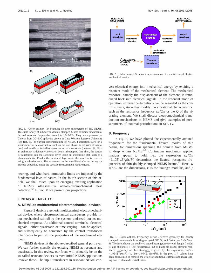
Figure 1 shows a family of semiconductor NEMS andoutlines their generic fabrication steps. This process for pat-terning freely suspended nanometer scale semiconductorstructures is referred to as surface nanomachining—as op-posed to the bulk micromachining of MEMS. These tech-niques apply to silicon on insulator structures,3 galliumarsenide/aluminum arsenidesGaAs/AlGaAsd systems,4 sili-con carbidesSiCd on silicon,5 aluminum nitride on silicon,6
nanocrystalline diamond films,7 and amorphous silicon ni-tride films.8 Most of these materials are available with high
purity, grown with a precise control of the layer thicknesses.This latter aspect yields dimensional control in the verticalsout-of-planed dimension at the monolayer level. This isnicely compatible with the lateral dimensional precision ofelectron beam lithography that approaches the atomic scale.
NEMS have a host of intriguing attributes. They offeraccess to a parameter space that is unprecedented: fundamen-tal resonance frequencies in the microwaves,9 mechanicalquality sQd factors in the tens of thousands,10 active massesin the femtograms, heat capacities far below a yoctocalorie11—this list goes on. These attributes spark the imagi-nation, and a flood of ideas for exciting experiments andapplications ensues—but a multitude of unanticipated ques-tions and concerns accompanies: How shall transducers berealized at the nanoscale? How shall surface properties becontrolled? How can reproducible nanofabrication be at-tained? To what extent can continuum theory be pushed intothe nanoregime to describe the mechanics of NEMS?Clearly, the characteristic parameters of NEMS are extremeby any measure. Those who would develop the next genera-tion NEMS must advance into the frontiers of physics andengineering in several directions at once.
This review is in four main sections. In the followingtwo sections, we shall attempt to convey a balanced intro-duction to NEMS. We shall not only discuss the excitingattributes of NEMS, but also give a survey of the existingtechnological and fundamental challenges in the field. As wemove forward, it will become increasingly apparent which ofthese challenges will be negotiable through systematic engi-
adAuthor to whom correspondence should be addressed; electronic mail:[email protected]
neering, and what hard, immutable limits are imposed by thefundamental laws of nature. In the fourth section of this ar-ticle, we shall touch upon an emerging exciting applicationof NEMS: ultrasensitive nanoelectromechanical massdetection.12 In Sec. V we present our projections.
II. NEMS ATTRIBUTES
A. NEMS as multiterminal electromechanical devices
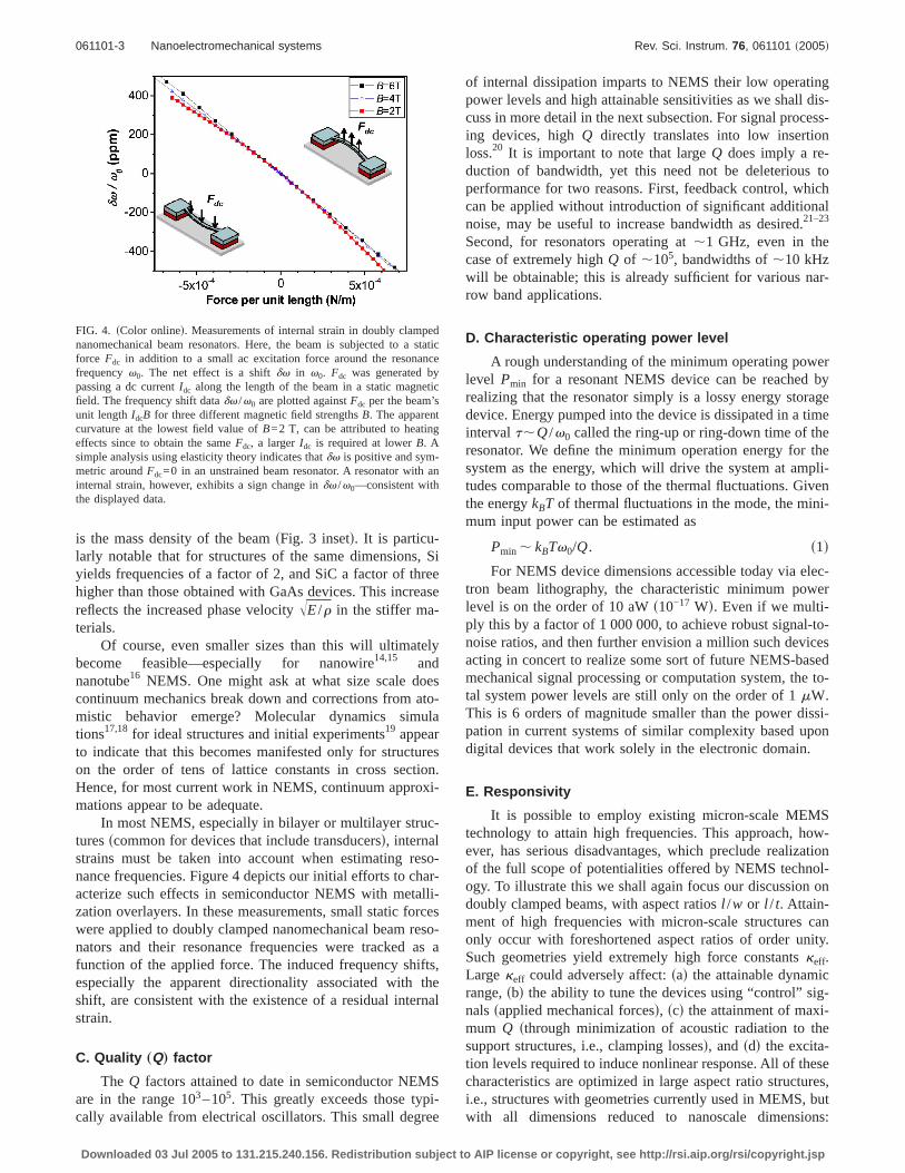
Figure 2 depicts a generic multiterminal electromechani-cal device, where electromechanical transducers provide in-put mechanical stimuli to the system, and read out its me-chanical response. At additional control terminals, electricalsignals—either quasistatic or time varying—can be applied,and subsequently be converted by the control transducersinto forces to perturb the properties of the mechanical ele-ment.
NEMS devices fit the above-described general portrayal.We can further classify the existing NEMS as resonant andquasistatic. In this review, our focus will primarily be on theso-called resonant devices as most initial NEMS applicationsinvolve these. The input transducers in resonant NEMS con-
vert electrical energy into mechanical energy by exciting aresonant mode of the mechanical element. The mechanicalresponse, namely the displacement of the element, is trans-duced back into electrical signals. In the resonant mode ofoperation, external perturbations can be regarded as the con-trol signals, since they modify the vibrational characteristics,such as the resonance frequencyv0/2p or the Q of the vi-brating element. We shall discuss electromechanical trans-duction mechanisms in NEMS and give examples of mea-surements of external perturbations in Sec. IV.
B. Frequency
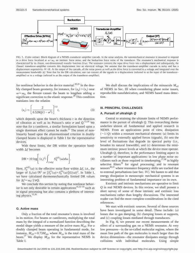
In Fig. 3, we have plotted the experimentally attainedfrequencies for the fundamental flexural modes of thinbeams, for dimensions spanning the domain from MEMSto deep within NEMS.5,9 Continuum mechanics approximations appear to hold, i.e., the expressionv0/2p=s1.05dÎE/rst / l2d determines the flexural resonance fre-quencies of thin doubly clamped NEMS beams.13 Here, w3 t3 l are the dimensions,E is the Young’s modulus, andr
FIG. 1. sColor onlined. sad Scanning electron micrograph of SiC NEMS.This first family of submicron doubly clamped beams exhibits fundamentalflexural resonant frequencies from 2 to 134 MHz. They were patterned atCaltech from 3C–SiC epilayers grown at Case Western Reserve Universityssee Ref. 5d. sbd Surface nanomachining of NEMS. Fabrication starts on asemiconductor heterostructure such as the one shown insid with structuralstopd and sacrificialsmiddled layers on top of a substratesbottomd. sii d Firstan etch mask is defined via electron beam lithography.siii d Then, the patternis transferred into the sacrificial layer using an anisotropic etch such as aplasma etch.sivd Finally, the sacrificial layer under the structure is removedusing a selective etch. The structures can be metallized after or during theprocess depending upon the specific measurement requirements.
FIG. 2. sColor onlined. Schematic representation of a multiterminal electro-mechanical device.
FIG. 3. sColor onlined. Frequency versus effective geometry for doublyclamped beams made from single-crystal SiC, Si, and GaAsssee Refs. 5 and9d. The inset shows the doubly clamped beam geometry with lengthl, widthw, and thicknesst. The fundamental out-of-planesin-planed flexural reso-nance frequency of this structure is given by the expression,v0/2p
=1.05ÎE/rst / l2d sv0/2p=1.05ÎE/rsw/ l2dd. In the plot, t / l2 values havebeen normalized to remove the effect of additional stiffness and mass load-ing due to electrode metallization.
061101-2 K. L. Ekinci and M. L. Roukes Rev. Sci. Instrum. 76, 061101 ~2005!
Downloaded 03 Jul 2005 to 131.215.240.156. Redistribution subject to AIP license or copyright, see http://rsi.aip.org/rsi/copyright.jsp
is the mass density of the beamsFig. 3 insetd. It is particu-larly notable that for structures of the same dimensions, Siyields frequencies of a factor of 2, and SiC a factor of threehigher than those obtained with GaAs devices. This increasereflects the increased phase velocityÎE/r in the stiffer ma-terials.
Of course, even smaller sizes than this will ultimatelybecome feasible—especially for nanowire14,15 andnanotube16 NEMS. One might ask at what size scale doescontinuum mechanics break down and corrections from ato-mistic behavior emerge? Molecular dynamics simulations17,18 for ideal structures and initial experiments19 appearto indicate that this becomes manifested only for structureson the order of tens of lattice constants in cross section.Hence, for most current work in NEMS, continuum approxi-mations appear to be adequate.
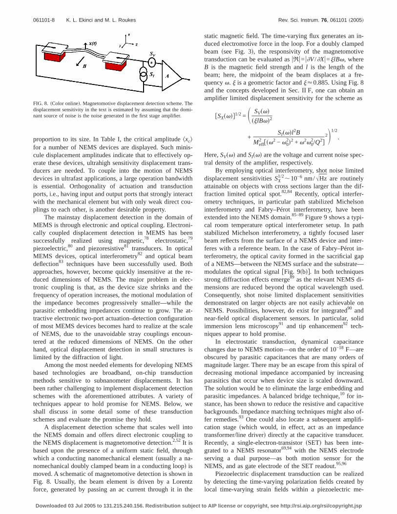
In most NEMS, especially in bilayer or multilayer struc-turesscommon for devices that include transducersd, internalstrains must be taken into account when estimating reso-nance frequencies. Figure 4 depicts our initial efforts to char-acterize such effects in semiconductor NEMS with metalli-zation overlayers. In these measurements, small static forceswere applied to doubly clamped nanomechanical beam reso-nators and their resonance frequencies were tracked as afunction of the applied force. The induced frequency shifts,especially the apparent directionality associated with theshift, are consistent with the existence of a residual internalstrain.
C. Quality „Q… factor
The Q factors attained to date in semiconductor NEMSare in the range 103–105. This greatly exceeds those typi-cally available from electrical oscillators. This small degree
of internal dissipation imparts to NEMS their low operatingpower levels and high attainable sensitivities as we shall dis-cuss in more detail in the next subsection. For signal process-ing devices, highQ directly translates into low insertionloss.20 It is important to note that largeQ does imply a re-duction of bandwidth, yet this need not be deleterious toperformance for two reasons. First, feedback control, whichcan be applied without introduction of significant additionalnoise, may be useful to increase bandwidth as desired.21–23
Second, for resonators operating at,1 GHz, even in thecase of extremely highQ of ,105, bandwidths of,10 kHzwill be obtainable; this is already sufficient for various nar-row band applications.
D. Characteristic operating power level
A rough understanding of the minimum operating powerlevel Pmin for a resonant NEMS device can be reached byrealizing that the resonator simply is a lossy energy storagedevice. Energy pumped into the device is dissipated in a timeintervalt,Q/v0 called the ring-up or ring-down time of theresonator. We define the minimum operation energy for thesystem as the energy, which will drive the system at ampli-tudes comparable to those of the thermal fluctuations. Giventhe energykBT of thermal fluctuations in the mode, the mini-mum input power can be estimated as
Pmin , kBTv0/Q. s1d
For NEMS device dimensions accessible today via elec-tron beam lithography, the characteristic minimum powerlevel is on the order of 10 aWs10−17 Wd. Even if we multi-ply this by a factor of 1 000 000, to achieve robust signal-to-noise ratios, and then further envision a million such devicesacting in concert to realize some sort of future NEMS-basedmechanical signal processing or computation system, the to-tal system power levels are still only on the order of 1mW.This is 6 orders of magnitude smaller than the power dissi-pation in current systems of similar complexity based upondigital devices that work solely in the electronic domain.
E. Responsivity
It is possible to employ existing micron-scale MEMStechnology to attain high frequencies. This approach, how-ever, has serious disadvantages, which preclude realizationof the full scope of potentialities offered by NEMS technol-ogy. To illustrate this we shall again focus our discussion ondoubly clamped beams, with aspect ratiosl /w or l / t. Attain-ment of high frequencies with micron-scale structures canonly occur with foreshortened aspect ratios of order unity.Such geometries yield extremely high force constantskeff.Largekeff could adversely affect:sad the attainable dynamicrange,sbd the ability to tune the devices using “control” sig-nalssapplied mechanical forcesd, scd the attainment of maxi-mum Q sthrough minimization of acoustic radiation to thesupport structures, i.e., clamping lossesd, andsdd the excita-tion levels required to induce nonlinear response. All of thesecharacteristics are optimized in large aspect ratio structures,i.e., structures with geometries currently used in MEMS, butwith all dimensions reduced to nanoscale dimensions:
FIG. 4. sColor onlined. Measurements of internal strain in doubly clampednanomechanical beam resonators. Here, the beam is subjected to a staticforce Fdc in addition to a small ac excitation force around the resonancefrequencyv0. The net effect is a shiftdv in v0. Fdc was generated bypassing a dc currentIdc along the length of the beam in a static magneticfield. The frequency shift datadv /v0 are plotted againstFdc per the beam’sunit lengthIdcB for three different magnetic field strengthsB. The apparentcurvature at the lowest field value ofB=2 T, can be attributed to heatingeffects since to obtain the sameFdc, a largerIdc is required at lowerB. Asimple analysis using elasticity theory indicates thatdv is positive and sym-metric aroundFdc=0 in an unstrained beam resonator. A resonator with aninternal strain, however, exhibits a sign change indv /v0—consistent withthe displayed data.
061101-3 Nanoelectromechanical systems Rev. Sci. Instrum. 76, 061101 ~2005!
Downloaded 03 Jul 2005 to 131.215.240.156. Redistribution subject to AIP license or copyright, see http://rsi.aip.org/rsi/copyright.jsp
NEMS. Calculatedkeff and other important parameters forseveral NEMS along with their dimensions are presented inTable I.
F. Available dynamic range
The linear dynamic rangesDRd is a widely used conceptin amplifier characterization, expressing the window of inputpower in which the amplifier behaves linearly. The bottom ofthe DR is determined by the noise power generated withinthe amplifiersreferred back to its inputd, and the top by thesinputd power level at which 1 dB compression occurs.
Similarly, we shall attempt to define a DR for a NEMSresonator as the ratio of its maximum vibration amplitudesatthe onset of nonlinearityd to its rms displacement noise floorwithin the operation bandwidthDf. In general, a NEMSresonator is always followed by a transducer-amplifier cas-cade. In most narrowband operation,Df is determined bythis transducer-amplifier cascade. One might sometimes de-sire to use the entire resonant response in which case themeasurement bandwidth becomes the naturalsnoised band-width of the resonatorDf <v0/2pQ.
The block diagram for a generic NEMS resonator oper-ated in its fundamental mode and coupled to a noisytransducer-amplifier cascade is shown in Fig. 5. The me-chanical response for the fundamental mode of the resonatorcan be approximated by that of a one-dimensional dampedharmonic oscillator with the following parameters: an effec-tive massMeff; an effective force constantsstiffnessd keff
=Meffv02; and a quality factorQ. The transfer functionGsvd
for the resonator then becomes
Gsvd =1
Meffsv02 − v2 + ivv0/Qd
. s2d
To retain the generality of the discussion, we shall as-sume that the resonator is driven by a noiseless drive force atv=v0, a dominant intrinsic noise and by the backactionforce of the transducer–amplifier. The drive has a force spec-tral densitykxdl2 dsv−v0d / uGsv0du2. kxdl is the rms vibrationamplitude to which the resonator is driven andkxdl is as-sumed to be within the linear regime of the resonator. Thepower spectral densitySF
sidsvd swith units N2/Hzd of the in-trinsic force noise term is determined by the dominant physi-cal noise mechanism. We shall have more to say about in-trinsic noise sources in NEMS in Sec. III B.SF
sbdsvdquantifies the force noise resulting from the backaction of thetransducer–amplifier cascade. The backaction force24 repre-
sents the reverse coupling and drives the mechanical elementas electrical impulses are generated in the transducer–amplifier cascade.
Apparently, the displacement noise floor, hence, the DRof the NEMS–transducer–amplifier cascade of Fig. 5 will bedetermined by the larger of the two distinct classes ofmechanisms—intrinsic noise processes fundamental to thenanomechanical resonator itself25,26 or extrinsic processesthat originate from the transducer–amplifier circuitry.27 Wenow obtain general expressions for the displacement noisefloor due to each process. The noise in the drive force gen-erates the rms displacement noise,
FE2pDf
fSFsidsvd + SF
sbdsvdguGsvdu2dvG1/2
.
Similarly, the voltage noise generated within the transducer–amplifier cascade withswhited spectral power densitySVsvdappears as a displacement noise at the input of the cascadewith an rms magnitude
FE2pDf
SVsvdR2 dvG1/2
.
Here, R=]V/]X is the cascade responsivityswith unitsV/md.
A very important conclusion can be reached based uponthe above discussion: the bottom segment of the availableDR will be forfeited unless optimal transducer–amplifier cas-cades are employed to read out the NEMS motion. To utilizethe full potential of NEMS, displacement transductionschemes are required that can provide resolution at the levelof the intrinsic displacement fluctuations without introducingsignificant backaction noise.
When extremely low noise transducer–amplifiers areavailable, the operation limits are usually set by the thermo-mechanical displacement fluctuations in the mechanical ele-ment. In Table I, we present the thermomechanical noiselevels for representative NEMS.SX
sthdsv0d is obtained23 bysetting SF
sidsvd=4Meffv0kBT/Q and evaluating SXsthdsv0d
=SFsidsv0duGsv0du2.Having established the noise floor or the bottom end of
the DR, we turn to the top end. The top end will be deter-mined by the critical drive amplitudekxcl at the onset ofnonlinearity. The source of nonlinearities in mechanical sys-tems can be geometric, inertial, or material in nature. There-fore, to establish this power level requires specific knowl-edge of the device geometry and the dominant mechanism
TABLE I. Important attributes for a family of doubly clamped Si beams withQ=10 000 atT=300 K. The effective force constantkeff=32Et3w/ l3 is definedfor point loading at the beam’s center. Nonlinear onset amplitudekxcl has been characterized using the criterion described in the text. The thermomechanicallylimited linear dynamic rangesDRd is calculated for the natural bandwidth of the beamDf <v0/2pQ and DR=20 logskxcl / kxthld, wherekxthl=skBT/keffd1/2.Effective mass for the fundamental mode isMeff<0.73Mtot whereMtot is the total mass of the beam.
061101-4 K. L. Ekinci and M. L. Roukes Rev. Sci. Instrum. 76, 061101 ~2005!
Downloaded 03 Jul 2005 to 131.215.240.156. Redistribution subject to AIP license or copyright, see http://rsi.aip.org/rsi/copyright.jsp
for nonlinear behavior in the device material.28,29 In the dou-bly clamped beam geometry, for instance, forkxdl. kxcl nearv<v0, the flexure causes the beam to lengthen adding asignificant correction to the elastic response.28 This conditiontranslates into the relation
kxcl < F 2
0.528Qs1 − s2dG1/2
t, s3d
which depends upon the beam’s thicknesst in the directionof vibration as well as its Poisson’s ratios and Q.15,30 Wenote that for a cantilever, a similar formulation based upon asingle dominant effect cannot be made.31 The onset of non-linearity based upon the aforementioned criterion in doublyclamped beams is displayed in Table I for the representativedevices.
With these limits, the DR within the operation band-width Df becomes
DR = 10 logFkxcl2/E2pDf
SXseffdsvddvG . s4d
Here,SXseffdsvd is the effective noise floor withinDf, i.e., the
larger of SVsvd /R2 or fSFsidsvd+SF
sbdsvdguGsvdu2. In Table I,we have calculated thermomechanically limited DR valuesfor Df <v0/2pQ.
We conclude this section by noting that nonlinear behav-ior is not only desirable in certain applications14,32–34such asin signal processing but also contains a plethora of interest-ing physics.35,36
G. Active mass
Only a fraction of the total resonator’s mass is involvedin its motion. For beams or cantilevers, multiplying the totalmass by the integral of a normalized function describing themodal shape yields a measure of the active massMeff. For adoubly clamped beam operating in fundamental mode, forinstance,Meff<0.73Mtot, whereMtot is the total mass of thebeam.37 We display Meff for the representative NEMS inTable I.
We shall discuss the implications of the minusculeMeff
of NEMS in Sec. III when considering phase noise issues,reproducible nanofabrication, and NEMS based mass detec-tion.
III. PRINCIPAL CHALLENGES
A. Pursuit of ultrahigh Q
Central to attaining the ultimate limits of NEMS perfor-mance is the pursuit of ultrahighQ. This overarching themeunderlies almost all fundamental and applied research inNEMS. From an applications point of view, dissipations,1/Qd within a resonant mechanical element:sad limits itssensitivity to externally applied forcesssignalsd, sbd sets thelevel of fluctuations that degrade its spectral puritysi.e.,broaden its natural linewidthd, and scd determines the mini-mum intrinsic power levels at which the device must operate.Ultrahigh Q, therefore, is the performance limiting aspect ina number of important applications: in low phase noise os-cillators such as those required in timekeeping;27,38 in highlyselective filters39 for signal processing; and in resonantsensors40,41where resonance frequency shifts are tracked dueto external perturbationsssee Sec. IVd. We hasten to add thatenergy dissipation in mesoscopic mechanical systems is aninteresting problem of fundamental importance on its own.
Extrinsic and intrinsic mechanisms are operative to limitQ in real NEMS devices. In this review, we shall present ashort survey of some of these intrinsic and extrinsic lossmechanisms rather than lengthy discussions. The interestedreader can find the more complete considerations in the citedreferences.
We start with extrinsic sources. Several of these sourceshave been investigated in some detail. These include:sadlosses due to gas damping,sbd clamping losses at supports,and scd coupling losses mediated through transducers.
In Fig. 6, we present our recent measurements of theeffect of a surrounding gas on a NEMS resonator. At verylow pressures—in the so-called molecular regime, where themean free path of the gas molecules is much larger than thedevice dimensions—the resonator dissipates energy throughcollisions with individual molecules. Using simple
FIG. 5. sColor onlined. Block diagram of a NEMS–transducer–amplifier cascade. In the noise analysis, the nanomechanical resonator is assumed to respondto a drive force localized atv=v0, an intrinsic force noise, and the backaction force noise of the transducer. The resonator’s mechanical response ischaracterized by itsslinear, one-dimensionald transfer functionGsvd. The resonator converts the input drive force into a displacement and subsequently, theslineard transducer–amplifier converts this displacement into an electrical voltage. We assume that the transducer–amplifier cascade is noisy and has adisplacement responsivity]V/]X. At the output of the cascade, all the noise power as well as the drive force is converted to a voltage and integrated over themeasurement bandwidthDf. Note that for the DR calculation, one can convert all the signals to a displacementsreferred to as the input of the transducer–amplifierd or to a voltagesreferred to as the output of the transducer–amplifierd.
061101-5 Nanoelectromechanical systems Rev. Sci. Instrum. 76, 061101 ~2005!
Downloaded 03 Jul 2005 to 131.215.240.156. Redistribution subject to AIP license or copyright, see http://rsi.aip.org/rsi/copyright.jsp
arguments,42–45a quality factor due to the gas dissipation canbe determined asQgas<Meffv0y /pA. Here,y=ÎkBT/m is thethermal velocity of the gas molecules each with massm, p isthe surrounding the gas pressure, andA is the surface area ofthe resonator. The so-called loadedQ of the device can thenbe determined asQL=sQi
−1+Qgas−1 d−1, whereQi is the intrinsic
Q. In Fig. 6sad, we plotQgas−1 as a function ofp. At low p, Qgas
−1
depends linearly onp. At high p, a crossover into a viscousdissipation regime46 is apparent;Qgas
−1 ~p1/2. The same cross-over is also manifest in the resonance frequency shift,dv /v0, displayed in Fig. 6sbd. In the molecular regime, neg-ligible frequency shift is observed; in the viscous regime,mass loading reducesv0. This crossover pressure can bedetermined by comparing the sound wavelength in the me-dium to the mean free path of the gas molecules.47
A resonator can lose the energy in its resonant modes viathe acoustic coupling to its clamps.48–50Most high frequencyNEMS have been realized in the doubly clamped beam con-figuration ssee Fig. 3d. One of the possible reasons for thedecrease ofQ factor in these devices is the clamping lossintrinsic to the doubly clamped boundary condition. Recentdemonstration of augmented clamping loss in doublyclamped NEMS beam resonators agrees with this claim.Huang et al.51 have compared theQ factor from identicalnanomechanical beams with free–free and doubly clampedboundary conditions, clearly showing a,2.5-fold enhance-ment in theQ of the free–free beam.
The possibility exists that displacement transduction pro-cess itself may contribute to the dissipation,52,53 causing ap-parent changes in the observedQ—sometimes also called theloadedQ, QL. Cleland and Roukes,52 for instance, quantifiedthe contribution of the magnetomotive transduction circuitryto the observed dissipation in NEMS. They developed a tech-nique whereby the external electrical damping could be mea-sured and controlled locally, enabling the manipulation ofQL.
In looking at intrinsic dissipation sources, it is essentialto discriminate between energy dissipation that occurs in aperfect crystal lattice and energy dissipation that occurs in areal, imperfect crystal with bulk and surface defects. The lossmechanisms in a perfect crystal are fundamental. These im-pose the ultimate upper bounds to attainableQs; such pro-cesses include thermoelastic damping arising from anhar-monic coupling between mechanical modes and the phononreservoir,54 and losses due to electron–phonon and phonon–phonon interactions. The intrinsic mechanisms due to imper-fections in the crystal may be suppressed by careful choice ofmaterials, processes, and handling. These include anelasticlosses involving defects in the bulk55,56 and surfaces.
NEMS devices patterned from single crystal, ultrapureheterostructures can contain very fewseven zerod crystallo-graphic defects and impurities. Hence, the initial hope wasthat within small enough structures bulk acoustic energy lossprocesses should be suppressed and ultrahighQ factorsthereby attained. Surprisingly, to date, a wide collection ofNEMS resonators—fabricated from different materials andprocessed using different surface nanomachiningtechniques—have yielded relatively lowQ factors in the103–105 range.
There is overwhelming experimental evidence that sur-faces contribute to the energy dissipation in NEMS in adominant fashion. Surface treatment experiments in ultrahighvacuumsUHVd on nano- and micromechanical devices haveshown that surface oxides, defects, and adsorbates augmentthe energy dissipation. Annealing nanometrically thin Si can-tilevers in UHV,57,58for instance, increased theirQ factors by1 order of magnitude. In subsequent x-ray photoelectronspectroscopy experiments,59,60 removal of oxygen fromnanoscale cantilever surfaces was correlated with improve-ments in the mechanicalQ factor. More recently, methylmonolayers were shown to suppress dissipation in siliconmicromechanical devices.61 Figure 7 displays the rough trendthat seems to be manifest in mechanical resonators ingeneral—from those that are truly macroscopic in size, tothose well within the domain of NEMS. The maximum at-tainableQs seem to scale downward with linear dimension,i.e., volume-to-surface ratio. We note that theQ measure-
FIG. 6. sColor onlined. Effect of surrounding gas pressure upon the reso-nance parameters of a GaAs doubly clamped NEMS beam withv0/2p<4.38 MHz. The intrinsicQ of the device wasQi <104. QL anddv of thebeam were measured as a function of the gas pressure in the measurementchamber.Qgaswas later extracted usingQi. The measurement was done withHe3 and He4 gases. Note the crossover in the plots from the ideal gas regimeto the viscous regime.
FIG. 7. sColor onlined. Maximum reportedQ factors in monocrystallinemechanical resonators varying in size from the macroscale to nanoscale. Thedata follow a trend showing a decrease inQ factor that occurs roughly withlinear dimension, i.e., with increasing volume-to-surface ratio.
061101-6 K. L. Ekinci and M. L. Roukes Rev. Sci. Instrum. 76, 061101 ~2005!
Downloaded 03 Jul 2005 to 131.215.240.156. Redistribution subject to AIP license or copyright, see http://rsi.aip.org/rsi/copyright.jsp
ments in resonators compiled in Fig. 7 were done at differenttemperatures.62–68,3,2,69
Given what is known from electronic and photonic de-vice physics regarding oxidation and reconstruction of the Sisurface, it seems clear that the mechanical properties of thesmallest NEMS devices will deviate greatly from those inbulk. It may prove quite difficult to achieve ultrahighQ withsuch extreme surface-to-volume ratios, if only conventionalpatterning approaches are utilized. Surface passivation willundoubtedly become imperative for nanometer scale devices.
One might project that structures such as nanotubes andnanowires may well represent the ideal for NEMS, giventheir perfectly terminated surfaces. So far, however, the ex-isting technology of manipulating, anchoring, and measuringthe mechanical properties of nanotube16,70,71 andnanowire14,15 devices is still quite primitive. Hence, there iscurrently insufficient information available even to permit acrude extrapolation of theQs that might ultimately be attain-able at high frequencies with nanotube and nanowire basedNEMS.
B. Phase noise
As mentioned above, resonant NEMS devices are envi-sioned in most initial applications—as high stability oscilla-tors in frequency clocks,26,27as highly selective filters in sig-nal processing,39 and as ultrasensitive sensors.12 In all ofthese, the short- and long-term resonance frequency stabilityof the resonator is central in establishing the operationlimits.72 Here, we turn to a discussion of the phase noiseprocesses and frequency stability in NEMS resonators.
The frequency stability of a resonator–transducer–amplifier cascadessee the discussion in Sec. II F and Fig. 5d
is determined by extrinsic processes in the transducercircuitry27,23 and intrinsic processes fundamental to the reso-nator itself.25,38The frequency stability in macro- and micro-mechanical resonators have, in most cases to date, been lim-ited by extrinsic elements, such as the transducer–amplifiercascade. In the domain of NEMS, however, given the en-hanced sensitivity that is attainable as devices becomesmaller and as ultrasensitive displacement transduction tech-niques emerge, fundamental fluctuation processes are in-creasingly likely to determine the outcome.
In a recent article,25 Cleland and Roukes have obtainedexpressions for phase noise in NEMS originating from a va-riety of intrinsic physical processes. In a subsequent article,Ekinci et al.37 converted the phase noise in Ref. 25 intofrequency fluctuations for specific measurement schemes.Later, the formalism was extended to extrinsic processes.12
Table II summarizes these recent results of the functionalforms of the spectral density of the frequency fluctuationssphase noised Svsvd and the corresponding frequency fluc-tuationsdv0<fe2pDfSvsvddvg1/2 for these processes. In thefirst row of Table II, amplifier transducer dominated fre-quency stability is presented. The intrinsic processes consid-ered in the subsequent rows include the thermomechanicalnoise generated by the internal loss mechanisms in the reso-nator, temperature fluctuations caused by the finite thermalconductance of the resonator,25 adsorption–desorptionnoise,73–75 and momentum exchange noise76,77 from sur-rounding gas molecules.
C. Development of transducers
The rms vibration amplitude for a mechanical devicesoperating within its linear ranged scales downward in direct
TABLE II. Expressions for NEMS phase noiseSvsvd and frequency fluctuationsdv0 for different noise mechanisms.dv0 are given for a measurementbandwidthDf. The resonator is assumed to be driven to its critical drive amplitudekxcl characterized by an energyEc=Meffv0
2kxc2l. In the first row, theswhited
voltage noise generated in the transducer–amplifier cascade is the dominant noise source; the symbols used have been defined in Sec. II F. The DR here isamplifier limited, and DR=10 logfkxcl2/ sSVDf /R2dg. In the second row, we present frequency fluctuations due to thermomechanical noise. Here, the mea-surement scheme effectively determinesSvsvd, although the obtaineddv0 is scheme independent. In the third row, temperature fluctuations are considered.Here,cs is the temperature dependent speed of sound;aT=s1/ld]l /]T is the linear thermal expansion coefficient; andg andtT are the thermal conductance andthe thermal time constant for the nanostructure, respectively. In the fourth row, the noise presented arises from the adsorption–desorption of gas moleculesupon the resonator. To determine the adsorption–desorption noise, the surface is modeled as comprisingNa sites for the adsorption of molecules of massmwith socc
2 representing the variance in the occupation probability of a site;tr is the correlation time for an adsorption–desorption cycle. In the bottom row, themomentum exchange noise from impinging gas molecules has been calculated for the low pressure limit with the parameters defined in Sec. III A.
061101-7 Nanoelectromechanical systems Rev. Sci. Instrum. 76, 061101 ~2005!
Downloaded 03 Jul 2005 to 131.215.240.156. Redistribution subject to AIP license or copyright, see http://rsi.aip.org/rsi/copyright.jsp
proportion to its size. In Table I, the critical amplitudekxclfor a number of NEMS devices are displayed. Such minis-cule displacement amplitudes indicate that to effectively op-erate these devices, ultrahigh sensitivity displacement trans-ducers are needed. To couple into the motion of NEMSdevices in ultrafast applications, a large operation bandwidthis essential. Orthogonality of actuation and transductionports, i.e., having input and output ports that strongly interactwith the mechanical element but with only weak direct cou-plings to each other, is another desirable property.
The mainstay displacement detection in the domain ofMEMS is through electronic and optical coupling. Electroni-cally coupled displacement detection in MEMS has beensuccessfully realized using magnetic,78 electrostatic,79
piezoelectric,80 and piezoresistive81 transducers. In opticalMEMS devices, optical interferometry82 and optical beamdeflection83 techniques have been successfully used. Bothapproaches, however, become quickly insensitive at the re-duced dimensions of NEMS. The major problem in elec-tronic coupling is that, as the device size shrinks and thefrequency of operation increases, the motional modulation ofthe impedance becomes progressively smaller—while theparasitic embedding impedances continue to grow. The at-tractive electronic two-port actuation–detection configurationof most MEMS devices becomes hard to realize at the scaleof NEMS, due to the unavoidable stray couplings encoun-tered at the reduced dimensions of NEMS. On the otherhand, optical displacement detection in small structures islimited by the diffraction of light.
Among the most needed elements for developing NEMSbased technologies are broadband, on-chip transductionmethods sensitive to subnanometer displacements. It hasbeen rather challenging to implement displacement detectionschemes with the aforementioned attributes. A variety oftechniques appear to hold promise for NEMS. Below, weshall discuss in some detail some of these transductionschemes and evaluate the promise they hold.
A displacement detection scheme that scales well intothe NEMS domain and offers direct electronic coupling tothe NEMS displacement is magnetomotive detection.2,52 It isbased upon the presence of a uniform static field, throughwhich a conducting nanomechanical elementsusually a na-nomechanical doubly clamped beam in a conducting loopd ismoved. A schematic of magnetomotive detection is shown inFig. 8. Usually, the beam element is driven by a Lorentzforce, generated by passing an ac current through it in the
static magnetic field. The time-varying flux generates an in-duced electromotive force in the loop. For a doubly clampedbeam ssee Fig. 3d, the responsivity of the magnetomotivetransduction can be evaluated asuRu= u]V/]Xu=jlBv, whereB is the magnetic field strength andl is the length of thebeam; here, the midpoint of the beam displaces at a fre-quencyv. j is a geometric factor andj<0.885. Using Fig. 8and the concepts developed in Sec. II F, one can obtain anamplifier limited displacement sensitivity for the scheme as
fSXsvdg1/2 = S SVsvdsjlBvd2
+SIsvdl2B
Meff2 fsv2 − v0
2d2 + v2v02/Q2g
2D1/2
.
Here,SVsvd andSIsvd are the voltage and current noise spec-tral density of the amplifier, respectively.
By employing optical interferometry, shot noise limiteddisplacement sensitivitiesSX
1/2,10−6 nm/ÎHz are routinelyattainable on objects with cross sections larger than the dif-fraction limited optical spot.82,84 Recently, optical interfer-ometry techniques, in particular path stabilized Michelsoninterferometry and Fabry–Pérot interferometry, have beenextended into the NEMS domain.85–89Figure 9 shows a typi-cal room temperature optical interferometer setup. In pathstabilized Michelson interferometry, a tightly focused laserbeam reflects from the surface of a NEMS device and inter-feres with a reference beam. In the case of Fabry–Pérot in-terferometry, the optical cavity formed in the sacrificial gapof a NEMS—between the NEMS surface and the substrate—modulates the optical signalfFig. 9sbdg. In both techniquesstrong diffraction effects emerge89 as the relevant NEMS di-mensions are reduced beyond the optical wavelength used.Consequently, shot noise limited displacement sensitivitiesdemonstrated on larger objects are not easily achievable onNEMS. Possibilities, however, do exist for integrated90 andnear-field optical displacement sensors. In particular, solidimmersion lens microscopy91 and tip enhancement92 tech-niques appear to hold promise.
In electrostatic transduction, dynamical capacitancechanges due to NEMS motion—on the order of 10−18 F—areobscured by parasitic capacitances that are many orders ofmagnitude larger. There may be an escape from this spiral ofdecreasing motional impedance accompanied by increasingparasitics that occur when device size is scaled downward.The solution would be to eliminate the large embedding andparasitic impedances. A balanced bridge technique,10 for in-stance, has been shown to reduce the resistive and capacitivebackgrounds. Impedance matching techniques might also of-fer remedies.93 One could also locate a subsequent amplifi-cation stageswhich would, in effect, act as an impedancetransformer/line driverd directly at the capacitive transducer.Recently, a single-electron-transistorsSETd has been inte-grated to a NEMS resonator69,94 with the NEMS electrodeserving a dual purpose—as both motion sensor for theNEMS, and as gate electrode of the SET readout.95,96
Piezoelectric displacement transduction can be realizedby detecting the time-varying polarization fields created bylocal time-varying strain fields within a piezoelectric me-
FIG. 8. sColor onlined. Magnetomotive displacement detection scheme. Thedisplacement sensitivity in the text is estimated by assuming that the domi-nant source of noise is the noise generated in the first stage amplifier.
061101-8 K. L. Ekinci and M. L. Roukes Rev. Sci. Instrum. 76, 061101 ~2005!
Downloaded 03 Jul 2005 to 131.215.240.156. Redistribution subject to AIP license or copyright, see http://rsi.aip.org/rsi/copyright.jsp
dium se.g., at points of high strain within a mechanical reso-natord. These polarization fields can be detected by placingthe gate of a field effect transistor97 or a single electrontransistor98 where the time-varying electric polarization islargest. Suspended high mobility electron structures havealso been exploited in the piezoelectric detection of nanos-cale motion.4,99 Piezoresistive detection100 is closely relatedto the piezoelectric detection scheme.
Electron tunneling is a technique that scales well, evendown to extremely small dimensions.101,102 However, be-cause the impedance of a tunnel junction is quite high, thebandwidth of such detectors is minimal in the presence ofunavoidable parasitic capacitance. We emphasize that thesebandwidth shortcomings are due to technological reasons,not fundamental ones. Quantum mechanical electron tunnel-ing in an atomic scale junction is an inherently fast phenom-enon with speeds much greater than 1 GHz.103 The nonlineardependence of the tunnel current upon the tunnel gap may
prove extremely useful for down conversion schemes100,104
in high frequency NEMS.
D. Reproducible nanofabrication
Surface nanomachining processes produce NEMS de-vices with large error margins in fundamental deviceparameters—even when identical processing parameters areemployed.9,10 This, in part, is an adverse consequence of theminiscule NEMS effective massesssee Table Id. Device trim-ming is ubiquitous in quartz frequency control technology. Itis clear that such techniques will also be required for NEMS.
IV. AN EMERGING APPLICATION
Even at this early stage of development, it seems clearthat NEMS will ultimately find use in a broad range of ap-plications. Recent demonstrations of NEMS basedelectrometry,105 optomechanical,106 and electromechanicalsignal processing,107 and mass detection12,108–111 have at-tracted much attention. From a fundamental science point ofview, NEMS are opening up investigations of phonon medi-ated mechanical processes112–115and of the quantum behav-ior of mesoscopic mechanical systems.69,94,116In the remain-der of this section, we shall focus on a particular NEMSapplication: nanoelectromechanical mass detection. Our dis-cussion of NEMS based mass detection has several differentfacets. First, it outlines the ubiquitous resonant sensing con-cept. Second, it puts NEMS based mass detection into per-spective by demonstrating its sensitivity limits. Third, it pro-poses avenues for NEMS based mass spectrometry.
Resonant mass sensors operate by providing a frequencyshift dv that is directly proportional to the inertial massdmof the analyte accreted upon them. Given the mass respon-sivity RM =]v0/]Meff, dm can be determined as
dm< U ]Meff
]v0Udv = uRMu−1dv. s5d
Here, we assume that the system parameters are weaklycoupled for small changes, i.e.,]Meff /]keff<0. We can fur-ther determine thatRM =−sv0/2Meffd, and
dm< 2Meff
v0dv. s6d
Mass sensors with exquisite mass sensitivities basedupon the simple relation described by Eq.s6d have beendemonstrated and employed in many diverse fields of sci-ence and technology. Among the most sensitive are thosebased upon the acoustic vibratory modes of crystals,117,118
thin films,119 and micron-sized cantilevers.120–122 In all ofthese, the effective vibratory mass of the resonatorMeff andthe minimum resolvable frequency shiftdvmin by the mea-surement circuitry determine the ultimate mass sensitivitydmmin. The minusculeMeff of NEMS ssee Table Id, in con-junction with their highQs, translates into opportunities forunprecedented mass sensitivity at high operationalsreso-nanced frequencies—as demonstrated in our recentexperiments.12
Here, we shall briefly review these experiments in aneffort to facilitate further discussion. These initial
FIG. 9. sColor onlined. sad Schematic diagram of the free space optical setupin use at Boston Universityssee Ref. 89d. The optical interferometer ismounted on aXYZ translation stagesnot shownd. The interferometer com-prises various beamsplitterssBSsd, a reference mirrorsRMd, and a photode-tector sPDd. The probe beam used for NEMS displacement detection istightly focused on the device by a 503 objective lenssOLd with numericalaperturesNA=0.5d. The light reflecting from the NEMS is collected by thesame lens and interferes with the reference beam on the PD. A constantreference path length is maintained by using a low-pass filtersLPFd and apiezoelectric actuatorsPZAd. The dashed line indicates the portion of thesetup used for the Fabry–Perot cavity measurements; the reference arm ofthe optics is simply blocked in the measurements.sbd Top view and centercross section of a doubly clamped NEMS beam in relation to the optical spotwith Gaussian profile.
061101-9 Nanoelectromechanical systems Rev. Sci. Instrum. 76, 061101 ~2005!
Downloaded 03 Jul 2005 to 131.215.240.156. Redistribution subject to AIP license or copyright, see http://rsi.aip.org/rsi/copyright.jsp
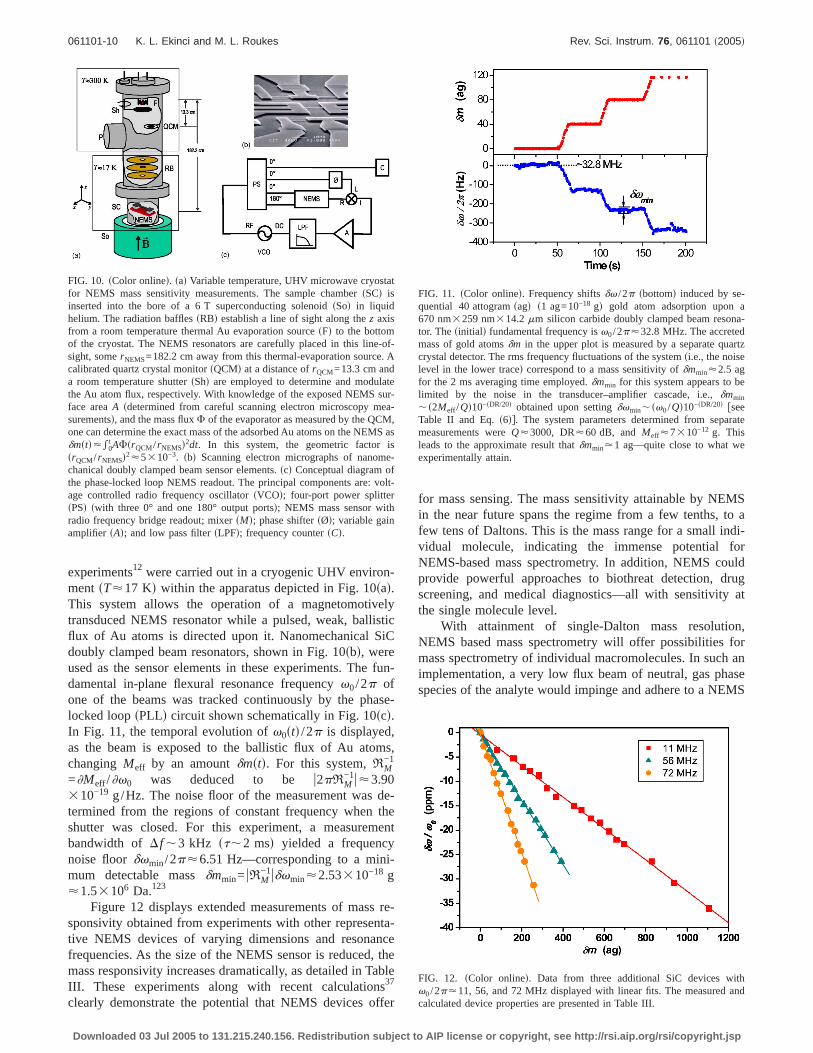
experiments12 were carried out in a cryogenic UHV environ-mentsT<17 Kd within the apparatus depicted in Fig. 10sad.This system allows the operation of a magnetomotivelytransduced NEMS resonator while a pulsed, weak, ballisticflux of Au atoms is directed upon it. Nanomechanical SiCdoubly clamped beam resonators, shown in Fig. 10sbd, wereused as the sensor elements in these experiments. The fun-damental in-plane flexural resonance frequencyv0/2p ofone of the beams was tracked continuously by the phase-locked loopsPLLd circuit shown schematically in Fig. 10scd.In Fig. 11, the temporal evolution ofv0std /2p is displayed,as the beam is exposed to the ballistic flux of Au atoms,changingMeff by an amountdmstd. For this system,RM
−1
=]Meff /]v0 was deduced to be u2pRM−1u<3.90
310−19 g/Hz. The noise floor of the measurement was de-termined from the regions of constant frequency when theshutter was closed. For this experiment, a measurementbandwidth of Df ,3 kHz st,2 msd yielded a frequencynoise floordvmin/2p<6.51 Hz—corresponding to a mini-mum detectable massdmmin= uRM
−1udvmin<2.53310−18 g<1.53106 Da.123
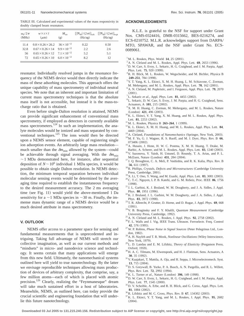
Figure 12 displays extended measurements of mass re-sponsivity obtained from experiments with other representa-tive NEMS devices of varying dimensions and resonancefrequencies. As the size of the NEMS sensor is reduced, themass responsivity increases dramatically, as detailed in TableIII. These experiments along with recent calculations37
clearly demonstrate the potential that NEMS devices offer
for mass sensing. The mass sensitivity attainable by NEMSin the near future spans the regime from a few tenths, to afew tens of Daltons. This is the mass range for a small indi-vidual molecule, indicating the immense potential forNEMS-based mass spectrometry. In addition, NEMS couldprovide powerful approaches to biothreat detection, drugscreening, and medical diagnostics—all with sensitivity atthe single molecule level.
With attainment of single-Dalton mass resolution,NEMS based mass spectrometry will offer possibilities formass spectrometry of individual macromolecules. In such animplementation, a very low flux beam of neutral, gas phasespecies of the analyte would impinge and adhere to a NEMS
FIG. 10. sColor onlined. sad Variable temperature, UHV microwave cryostatfor NEMS mass sensitivity measurements. The sample chambersSCd isinserted into the bore of a 6 T superconducting solenoidsSod in liquidhelium. The radiation bafflessRBd establish a line of sight along thez axisfrom a room temperature thermal Au evaporation sourcesFd to the bottomof the cryostat. The NEMS resonators are carefully placed in this line-of-sight, somerNEMS=182.2 cm away from this thermal-evaporation source. Acalibrated quartz crystal monitorsQCMd at a distance ofrQCM=13.3 cm anda room temperature shuttersShd are employed to determine and modulatethe Au atom flux, respectively. With knowledge of the exposed NEMS sur-face areaA sdetermined from careful scanning electron microscopy mea-surementsd, and the mass fluxF of the evaporator as measured by the QCM,one can determine the exact mass of the adsorbed Au atoms on the NEMS asdmstd<e0
t AFsrQCM/ rNEMSd2dt. In this system, the geometric factor issrQCM/ rNEMSd2<5310−3. sbd Scanning electron micrographs of nanome-chanical doubly clamped beam sensor elements.scd Conceptual diagram ofthe phase-locked loop NEMS readout. The principal components are: volt-age controlled radio frequency oscillatorsVCOd; four-port power splittersPSd swith three 0° and one 180° output portsd; NEMS mass sensor withradio frequency bridge readout; mixersMd; phase shiftersØd; variable gainamplifier sAd; and low pass filtersLPFd; frequency countersCd.
FIG. 11. sColor onlined. Frequency shiftsdv /2p sbottomd induced by se-quential 40 attogramsagd s1 ag=10−18 gd gold atom adsorption upon a670 nm3259 nm314.2mm silicon carbide doubly clamped beam resona-tor. Thesinitiald fundamental frequency isv0/2p<32.8 MHz. The accretedmass of gold atomsdm in the upper plot is measured by a separate quartzcrystal detector. The rms frequency fluctuations of the systemsi.e., the noiselevel in the lower traced correspond to a mass sensitivity ofdmmin<2.5 agfor the 2 ms averaging time employed.dmmin for this system appears to belimited by the noise in the transducer–amplifier cascade, i.e.,dmmin
,s2Meff /Qd10−sDR/20d obtained upon settingdvmin,sv0/Qd10−sDR/20d fseeTable II and Eq.s6dg. The system parameters determined from separatemeasurements wereQ<3000, DR<60 dB, and Meff<7310−12 g. Thisleads to the approximate result thatdmmin<1 ag—quite close to what weexperimentally attain.
FIG. 12. sColor onlined. Data from three additional SiC devices withv0/2p<11, 56, and 72 MHz displayed with linear fits. The measured andcalculated device properties are presented in Table III.
061101-10 K. L. Ekinci and M. L. Roukes Rev. Sci. Instrum. 76, 061101 ~2005!
Downloaded 03 Jul 2005 to 131.215.240.156. Redistribution subject to AIP license or copyright, see http://rsi.aip.org/rsi/copyright.jsp
resonator. Individually resolved jumps in the resonance fre-quency of the NEMS device would then directly indicate themass of these adsorbing molecules. This approach offers theunique capability of mass spectrometry of individual neutralspecies. We note that an inherent and important limitation ofcurrent mass spectrometry techniques is that the absolutemass itself is not accessible, but instead it is the mass-to-charge ratio that is obtained.
Even before single-Dalton resolution is attained, NEMScan provide significant enhancement of conventional massspectrometry, if employed as detectors in currently availablemass spectrometers.124 In such an implementation, the ana-lyte molecules would be ionized and mass separated by con-ventional techniques.125 The ions would then be directedupon a NEMS sensor element, capable of registering singleion adsorption events. An arbitrarily large mass resolution—much smaller than thedmmin allowed by the system—couldbe achievable through signal averaging. With thedmmin
,1 MDa demonstrated here, for instance, after sequentialdeposition ofN,106 individual 1 MDa species, it would bepossible to obtain single Dalton resolution. In NEMS detec-tion, the minimum temporal separation between individualmolecular sensing events would be determined by the aver-aging time required to establish the instantaneous frequencyto the desired measurement accuracy. The 2 ms averagingtime ssee Fig. 11d would yield the above-mentioned 1 Dasensitivity for a,1 MDa species in,30 m. Finally, the im-mense mass dynamic range of a NEMS device would be amuch desired attribute in mass spectrometry.
V. OUTLOOK
NEMS offer access to a parameter space for sensing andfundamental measurements that is unprecedented and in-triguing. Taking full advantage of NEMS will stretch ourcollective imagination, as well as our current methods and“mindsets” in micro- and nanodevice science and technol-ogy. It seems certain that many applications will emergefrom this new field. Ultimately, the nanomechanical systemsoutlined here will yield to true nanotechnology. By the latterwe envisage reproducible techniques allowing mass produc-tion of devices of arbitrary complexity, that comprise, say, afew million atoms—each of which is placed with atomicprecision.126 Clearly, realizing the “Feynmanesque” dreamwill take much sustained effort in a host of laboratories.Meanwhile, NEMS, as outlined here, can today provide thecrucial scientific and engineering foundation that will under-lie this future nanotechnology.
ACKNOWLEDGMENTS
K.L.E. is grateful to the NSF for support under GrantNos. CMS-0324416, DMR-0315662, BES-0216274, andECS-0210752. M.L.R. acknowledges support from DARPA/MTO, SPAWAR, and the NSF under Grant No. ECS-0089061.
1M. L. Roukes, Phys. World14, 25 s2001d.2A. N. Cleland and M. L. Roukes, Appl. Phys. Lett.69, 2653s1996d.3D. W. Carr, S. Evoy, L. Sekaric, H. G. Craighead, and J. M. Parpia, Appl.Phys. Lett. 75, 920 s1999d.
4R. H. Blick, M. L. Roukes, W. Wegscheider, and M. Bichler, Physica B249–251, 784 s1998d.
5Y. T. Yang, K. L. Ekinci, X. M. H. Huang, L. M. Schiavone, C. Zorman,M. Mehregany, and M. L. Roukes, Appl. Phys. Lett.78, 162 s2001d.
6A. N. Cleland, M. Pophristic, and I. Ferguson, Appl. Phys. Lett.79, 2070s2001d.
7L. Sekaricet al., Appl. Phys. Lett.81, 4455s2002d.8L. Sekaric, D. W. Carr, S. Evoy, J. M. Parpia, and H. G. Craighead, Sens.Actuators, A 101, 215 s2002d.
9X. M. H. Huang, C. Zorman, M. Mehregany, and M. L. Roukes, NaturesLondond 421, 496 s2003d.
10K. L. Ekinci, Y. T. Yang, X. M. Huang, and M. L. Roukes, Appl. Phys.Lett. 81, 2253s2002d.
11M. L. Roukes, Physica B263–264, 1 s1999d.12K. L. Ekinci, X. M. H. Huang, and M. L. Roukes, Appl. Phys. Lett.84,
4469 s2004d.13A. Cleland,Foundations of NanomechanicssSpringer, New York, 2003d.14M. F. Yu, G. J. Wagner, R. S. Ruoff, and M. J. Dyer, Phys. Rev. B66,
073406s2002d.15A. Husain, J. Hone, H. W. C. Postma, X. M. H. Huang, T. Drake, M.
Barbic, A. Scherer, and M. L. Roukes, Appl. Phys. Lett.83, 1240s2003d.16V. Sazonova, Y. Yaish, H. Ustunel, D. Roundy, T. A. Arias, and P. L.
McEuen, NaturesLondond 431, 284 s2004d.17J. Q. Broughton, C. A. Meli, P. Vashishta, and R. K. Kalia, Phys. Rev. B
56, 611 s1997d.18R. Phillips,Crystals, Defects and MicrostructuressCambridge University
Press, Cambridge, 2001d.19X. Li, T. Ono, Y. Wang, and M. Esashi, Appl. Phys. Lett.83, 3081s2003d.20C. T.-C. Nguyen, L P. B. Katehi, and G. M. Rebeiz, Proc. IEEE86, 1756
s1998d.21J. L. Garbini, K. J. Bruland, W. M. Dougherty, and J. A. Sidles, J. Appl.
Phys. 80, 1951s1996d.22K. J. Bruland, J. L. Garbini, W. M. Dougherty, and J. A. Sidles, J. Appl.
Phys. 83, 3972s1998d.23T. R. Albrecht, P. Grutter, D. Horne, and D. Rugar, J. Appl. Phys.69, 668
s1991d.24V. B. Braginsky and F. Y. Khalili,Quantum MeasurementsCambridge
University Press, Cambridge, 1992d.25A. N. Cleland and M. L. Roukes, J. Appl. Phys.92, 2758s2002d.26F. L. Walls and J. Vig, IEEE Trans. Ultrason. Ferroelectr. Freq. Control
42, 576 s1995d.27W. P. Robins,Phase Noise in Signal SourcessPeter Pelegrinus Ltd., Lon-
don, 1982d.28A. H. Nayfeh and T. R. Mook,Nonlinear OscillationssWiley Interscience,
New York, 1979d.29L. D. Landau and E. M. Lifshitz,Theory of ElasticitysPergamon Press,
Oxford, 1959d.30H. A. C. Tilmans, M. Elwenspoek, and H. J. Flutiman, Sens. Actuators, A
30, 35 s1992d.31V. Kaajakari, T. Mattila, A. Oja, and H. Seppa, J. Microelectromech. Syst.
13, 715 s2004d.32D. S. Greywall, B. Yurke, P. A. Busch, A. N. Pargellis, and R. L. Willett,
Phys. Rev. Lett.72, 2992s1994d.33K. L. Turner et al., NaturesLondond 396, 149 s1998d.34D. W. Carr, S. Evoy, L. Sekaric, H. G. Craighead, and J. M. Parpia, Appl.
Phys. Lett. 77, 1545s2000d.35D. V. Scheible, A. Erbe, and R. H. Blick, and G. Corso, Appl. Phys. Lett.
81, 1884s2002d.36R. Lifshitz and M. C. Cross, Phys. Rev. B67, 134302s2003d.37K. L. Ekinci, Y. T. Yang, and M. L. Roukes, J. Appl. Phys.95, 2682
s2004d.
TABLE III. Calculated and experimental values of the mass responsivity indoubly clamped beam resonators.
061101-11 Nanoelectromechanical systems Rev. Sci. Instrum. 76, 061101 ~2005!
Downloaded 03 Jul 2005 to 131.215.240.156. Redistribution subject to AIP license or copyright, see http://rsi.aip.org/rsi/copyright.jsp
38J. R. Vig and Y. Kim, IEEE Trans. Ultrason. Ferroelectr. Freq. Control46,1558s1999d.
39K. Wang and C. T.-C. Nguyen, Proceedings, 1997 IEEE InternationalMicro Electro Mechanical Systems Workshop, Nagoya, Japan, Jan. 26–30,1997, pp. 25–30.
40T. D. Stowe, K. Yasumura, T. W. Kenny, D. Botkin, K. Wago, and D.Rugar, Appl. Phys. Lett.71, 288 s1997d.
41M. M. Midzor et al., J. Appl. Phys.87, 6493s2000d.42K. Kokubun, M. Hirata, M. Ono, H. Murakami, and Y. Toda, J. Vac. Sci.
Technol. A 5, 2450s1987d.43F. R. Blom, S. Bouwstra, M. Elwenspoek, and J. H. J. Fluitman, J. Vac.
Sci. Technol. B10, 19 s1992d.44K. Yum et al., J. Appl. Phys.96, 3933s2004d.45R. B. Bhiladvala and Z. J. Wang, Phys. Rev. E69, 036307s2004d.46L. D. Landau,Fluid MechanicssPergamon, Oxford, 1982d.47V. B. Braginsky, V. P. Mitrofanov, and V. I. Panov,Systems with Small
DissipationsThe University of Chicago Press, Chicago, 1985d.48M. C. Cross and R. Lifshitz, Phys. Rev. B64, 085324s2001d.49D. M. Photiadis and J. A. Judge, Appl. Phys. Lett.85, 482 s2004d.50H. Jiang, M.-F. Yu, B. Liu, and Y. Huang, Phys. Rev. Lett.93, 185501
s2004d.51X. M. H. Huang, M. K. Prakash, C. A. Zorman, M. Mehregany, and M. L.
Roukes, TRANSDUCERS ’03 Proceedings 12th International Conferenceon Solid State Sensors, Actuators and Microsystems, Boston, June 8–12,2003.
52A. N. Cleland and M. L. Roukes, Sens. Actuators, A72, 256 s1999d.53K. C. Schwab, Appl. Phys. Lett.80, 1276s2002d.54R. Lifshitz and M. L. Roukes, Phys. Rev. B61, 5600s2000d.55A. B. Hutchinson, P. A. Truitt, K. C. Schwab, L. Sekaric, J. M. Parpia, H.
G. Craighead, and J. E. Butler, Appl. Phys. Lett.84, 972 s2004d.56S. Evoy, A. Olkhovets, L. Sekaric, J. M. Parpia, H. G. Craighead, and D.
W. Carr, Appl. Phys. Lett.77, 2397s2000d.57K. Y. Yasumura, T. D. Stowe, E. M. Chow, T. Pfafman, T. W. Kenny, B.
C. Stipe, and D. Rugar, J. Microelectromech. Syst.9, 117 s2000d.58K. Y. Yasumura, T. D. Stowe, E. M. Chow, T. Pfafman, T. W. Kenny, and
D. Rugar,Proceedings Technical Digest of the 1998 Solid-State Sensorand Actuator Workshop, Hilton Head Island, SC, June 8–11, 1998sTrans-ducer Research Foundation, Cleveland, 1998d.
59J. Yang, T. Ono, and M. Esashi, Appl. Phys. Lett.77, 3860s2000d.60J. Yang, T. Ono, and M. Esashi, J. Vac. Sci. Technol. B19, 551 s2001d.61Y. Wang, J. A. Henry, D. Sengupta, and M. A. Hines, Appl. Phys. Lett.
85, 5736s2004d.62D. F. Mcguigan, C. C. Lam, R. Q. Gram, A. W. Hoffman, D. H. Douglass,
and H. W. Gutche, J. Low Temp. Phys.30, 621 1978.63R. N. Kleiman, G. Agnolet, and D. J. Bishop, Phys. Rev. Lett.59, 2079
s1987d.64T. Klistner and R. O. Pohl, Phys. Rev. B36, 6551s1987d.65William Duffy, Jr., J. Appl. Phys.68, 5601s1990d.66R. A. Buser and N. F. de Rooij, Sens. Actuators, A21, 323 s1990d.67D. S. Greywall, B. Yurke, P. A. Busch, and S. C. Arney, Europhys. Lett.
34, 37 s1996d.68R. E. Mihailovich and J. M. Parpia, Phys. Rev. Lett.68, 3052s1992d.69M. D. LaHaye, O. Buu, B. Camarota, and K. C. Schwab, Science304, 74
s2004d.70H. Dai, Phys. World13, 43 s2000d.71J. Chung, K.-H. Lee, J. Lee, and R. S. Ruoff, Langmuir20, 3011s2004d.72T. H. Lee and A. Hajimiri, IEEE J. Solid-State Circuits35, 326 s2000d.73Y. K. Yong and J. R. Vig, IEEE Trans. Ultrason. Ferroelectr. Freq. Control
36, 452 s1989d.74Y. K. Yong and J. R. Vig, IEEE Trans. Ultrason. Ferroelectr. Freq. Control
s2002d.76W. Gerlach, Naturwiss.15, 15 s1927d.77G. E. Uhlenbeck and S. Goudsmit, Phys. Rev.34, 145 s1929d.78D. S. Greywall, B. Yurke, P. A. Busch, A. N. Pargellis, and R. L. Willett,
Phys. Rev. Lett.72, 2992s1992d.79W. C. Tang, T. C. H. Nguyen, M. W. Judy, and R. T. Howe, Sens. Actua-
tors, A 21, 328 s1990d.80J. Soderkvist and K. Hjort, J. Micromech. Microeng.4, 28 s1994d.81M. Tortonese, R. C. Barret, and C. F. Quate, Appl. Phys. Lett.62, 834
s1993d.82J. W. Wagner, Phys. Acoust.19, 201 s1990d.
83T. G. Bifano, J. Perreault, R. K. Mali, and M. N. Horenstein, IEEE J. Sel.Top. Quantum Electron.5, 83 s1999d.
84T. R. Albrecht, P. Grütter, D. Rugar, and D. P. E. Smith, Ultramicroscopy42, 1638s1992d.
85D. W. Carr, L. Sekaric, and H. G. Craighead, J. Vac. Sci. Technol. B16,3821 s1998d.
86D. W. Carr, S. Evoy, L. Sekaric, A. Olkhovets, J. M. Parpia, and H. G.Craighead, Appl. Phys. Lett.77, 1545s2000d.
87C. Meyer, H. Lorenz, and K. Karrai, Appl. Phys. Lett.83, 2420s2003d.88B. E. N. Keeler, D. W. Carr, J. P. Sullivan, T. A. Friedmann, and J. R.
Wendt, Opt. Lett.29, 1182s2004d.89T. Kouh, D. Karabacak, D. H. Kim, and K. L. Ekinci, Appl. Phys. Lett.
86, 013106s2005d.90E. Ollier, IEEE J. Sel. Top. Quantum Electron.8, 155 s2002d.91S. B. Ippolito, B. B. Goldberg, and M. S. Unlu, Appl. Phys. Lett.78, 4071
s2001d.92E. J. Sánchez, L. Novotny, and X. S. Xie, Phys. Rev. Lett.82, 4014
s1999d.93P. A. Truitt, J. Hertzberg, and K. C. Schwab, Bull. Am. Phys. Soc.50,
1307 s2005d.94R. G. Knobel and A. N. Cleland, NaturesLondond 424, 291 s2003d.95M. P. Blencowe, Proc. SPIE5115, 64 s2003d.96M. P. Blencowe and M. N. Wybourne, Appl. Phys. Lett.77, 3845s2000d.97R. G. Beck, M. A. Eriksson, and R. M. Westervelt, Appl. Phys. Lett.73,
1149 s1998d.98R. Knobel and A. N. Cleland, Appl. Phys. Lett.81, 2258s2002d.99H. X. Tang, X. M. H. Huang, M. L. Roukes, M. Bichler, and W. Wegsc-
heider, Appl. Phys. Lett.81, 3879s2002d.100I. Bargatin, E. B. Myers, J. Arlett, B. Gudlewski, and M. L. Roukes,
Appl. Phys. Lett.86, 133109s2005d.101M. F. Bocko, Rev. Sci. Instrum.61, 3763s1990d.102T. W. Kennyet al., J. Vac. Sci. Technol. A10, 2114s1992d.103G. Nunes, Jr. and M. R. Freeman, Science262, 1029s1993d.104A. N. Cleland, J. S. Aldridge, D. C. Driscoll, and A. C. Gossard, Appl.
Phys. Lett. 81, 1699s2002d.105A. N. Cleland and M. L. Roukes, NaturesLondond 392, 160 s1998d.106L. Sekaric, M. Zalalutdinov, S. W. Turner, A. T. Zehnder, J. M. Parpia,
and H. G. Craighead, Appl. Phys. Lett.80, 3617s2002d.107A. Erbe, H. Krömmer, A. Kraus, R. H. Blick, G. Corso, and K. Richter,
Appl. Phys. Lett.77, 3102s2000d.108M. L. Roukes and K. L. Ekinci, U. S. Patent 6,722,200s20 April 2004d.109B. Ilic, H. G. Craighead, S. Krylov, W. Senaratne, C. Ober, and P. Neuzil,
J. Appl. Phys.95, 3694s2004d.110N. V. Lavrik and P. G. Datskos, Appl. Phys. Lett.82, 2697s2003d.111A. Gupta, D. Akin, and R. Bashir, Appl. Phys. Lett.84, 1976s2004d.112T. S. Tighe, J. M. Worlock, and M. L. Roukes, Appl. Phys. Lett.70, 2687
s1997d.113K. C. Schwab, E. A. Henriksen, J. M. Worlock, and M. L. Roukes, Nature
sLondond 404, 974 s2000d.114C. S. Yung, D. R. Schmidt, and A. N. Cleland, Appl. Phys. Lett.81, 31
sElsevier, London, 1984d.118S. S. Narine and A. J. Slavin, J. Vac. Sci. Technol. A16, 1857s1998d.119M. Thompson and D. C. Stone,Surface-Launched Acoustic Wave Sen-
sors: Chemical Sensing and Thin-Film CharacterizationsWiley, NewYork, 1997d.
120T. Thundat, E. A. Wachter, S. L. Sharp, and R. J. Warmack, Appl. Phys.Lett. 66, 1695s1995d.
121B. Ilic et al., Appl. Phys. Lett.77, 450 s2000d.122Z. J. Daviset al., J. Vac. Sci. Technol. B18, 612 s2000d.123The SI defines 1 Da as 1/12 the mass of the C12 atom. 1 Da=1.66
310−27 kg124W. K. Hibert, X. L. Feng, and M. L. Roukes, Am. Phys. Soc.50, 1132
s2005d.125E. de Hoffmann and V. Stroobant,Mass Spectrometry Principles and
ApplicationssWiley, New York, 2002d.126R. P. Feynman,Proceeding of American Physical Society Meeting, Pasa-
dena, CA, December 29, 1959soriginally published in Caltech’sEngi-neering and Science magazine, Feb. 1960d; reprinted as R. P. Feynman, J.Microelectromech. Syst.2, 1 s1993d.
061101-12 K. L. Ekinci and M. L. Roukes Rev. Sci. Instrum. 76, 061101 ~2005!
Downloaded 03 Jul 2005 to 131.215.240.156. Redistribution subject to AIP license or copyright, see http://rsi.aip.org/rsi/copyright.jsp