Page 1/22 Design and Analysis of Various Solar Cell Technologies for Improvements in Eciencies: A Review Divya Sharma ( [email protected]) National Institute of Technical Teachers' Training and Research Chandigarh Rajesh Mehra National Institute of Technical Teachers' Training and Research Chandigarh Balwinder Raj National Institute of Technical Teachers' Training and Research Chandigarh Research Article Keywords: Current photovoltaic technologies, eciency, solar cells, thin lm solar cells, wafer silicon based solar cells Posted Date: May 6th, 2021 DOI: https://doi.org/10.21203/rs.3.rs-469458/v1 License: This work is licensed under a Creative Commons Attribution 4.0 International License. Read Full License
Transcript
Page 1/22
Design and Analysis of Various Solar CellTechnologies for Improvements in Eciencies: AReviewDivya Sharma ( [email protected] )
National Institute of Technical Teachers' Training and Research ChandigarhRajesh Mehra
National Institute of Technical Teachers' Training and Research ChandigarhBalwinder Raj
National Institute of Technical Teachers' Training and Research Chandigarh
Research Article
Keywords: Current photovoltaic technologies, eciency, solar cells, thin lm solar cells, wafer siliconbased solar cells
Posted Date: May 6th, 2021
DOI: https://doi.org/10.21203/rs.3.rs-469458/v1
License: This work is licensed under a Creative Commons Attribution 4.0 International License. Read Full License
AbstractSolar energy is an inexhaustible source of energy existing on earth. Sun annually delivers approximately10,000 times of energy that human race currently exploits. Being neat and clean, solar energy has steeredpath to redeem utilization of conventional resources of energy by birth of solar cells. Solar cells, modulesand Photovoltaic systems have been industrialized substantially since race to conquer outer space startedduring 1960s. Further, oil crisis in 1970s forced the nations to embrace solar technologies as alternativemeans for conventional sources of energy. Developments in cost ecacy, compact constructions,consistency and lifetime enabled photovoltaics to be the rst option for extensive range of uses in day today life. Photovoltaics are widely used in telecommunications, remote power and cathodic protection.Objective of this paper is to review developments of solar cells since its origin, with comprehensivedescription of manufacturing processes, implementations and power conversion eciencies of solar cellsof various generations including their future trends and aspects.
1. IntroductionPhotovoltaic is essentially an intensive technological approach to transform sunlight into electrical energy.Electricity, being the direct current, may be used as alternating current by converting it and can be storedfor further exploitation. Hypothetically, a photovoltaic cell is a device that only ingests sunlight and yieldselectricity. Absence of moving parts, at least not in the atomic way; makes its operation appropriate for theenvironment. Photovoltaic devices, being eco-friendly and non-toxic, are benecial and suitable forinhabitants of earth. Photovoltaic systems being exible by design, their power output may be engineeredfor almost every application i.e. from low powered consumer uses e.g. wrist-watches, toys calculators andbattery chargers to high power consumer uses e.g. solar panels of space satellites [1].
The vital parameters required to examine the capability of a solar cell are short-circuit current density(JSC), ll factor (FF), open-circuit voltage (VOC) & power conversion eciency (PCE). Figure 1 illustratesJSC-V aspects of a solar cell in dark and illuminated ambience. Short-circuit current density (JSC) iselaborated as the current generated by a solar cell under illuminated ambience in the absence of anyexternal load. Open circuit voltage (VOC) can be stated as the difference in potential across two terminalsof a solar cell under illuminated condition while no current passes across the terminals [2]. In Eq. 1, FillFactor (FF) can be elaborated as the ratio of maximum power (PMax) generated to the product of short-circuit current density (JSC) and open-circuit voltage (VOC) i.e.
FF = PMax / (JSC) × (VOC) (1)
Power conversion eciency of a PV cell is calculated as ratio of the maximum power generated by thesolar cell and the incident radiant energy.
2. Technologies Implemented In Solar Cells
Page 3/22
It has been experienced that present solar cells have some disadvantages but these would likely toastound with the advancement of new technologies. Subsequently, the cost of solar cells along withinstallation will decrease so that these cells will be within the reach of common man. Presently, search fornew materials with properties like low specic gravity, malleable, inexpensive and non-toxic are in progressto manufacture cheaper and reliable solar cells which have higher eciencies.
The journey of manufacturing processes w.r.t solar cells has seen numerous transformations startingfrom wafer silicon based to new emerging technology of third generation which is illustrated throughFig. 2 [3]. Developments of next generation solar cells have boosted the eciencies of these cells. Solarcells have been differentiated into a number of classes as per materials utilized which are elaborated inthe succeeding sections.
2.1 First Generation Solar Cells (Wafer Silicon Based)These cells can also be recognized as conventional/ traditional solar cells which are fabricated on thinsilicon layers called wafers. These cells are the most geriatric, also involve eminent technology due to itshigh energy conversion rates. These cells are further classied into-
2.1.1 Mono-crystalline/Single crystalline silicon solar cell
2.1.2 Polycrystalline/Multi-crystalline silicon solar cell
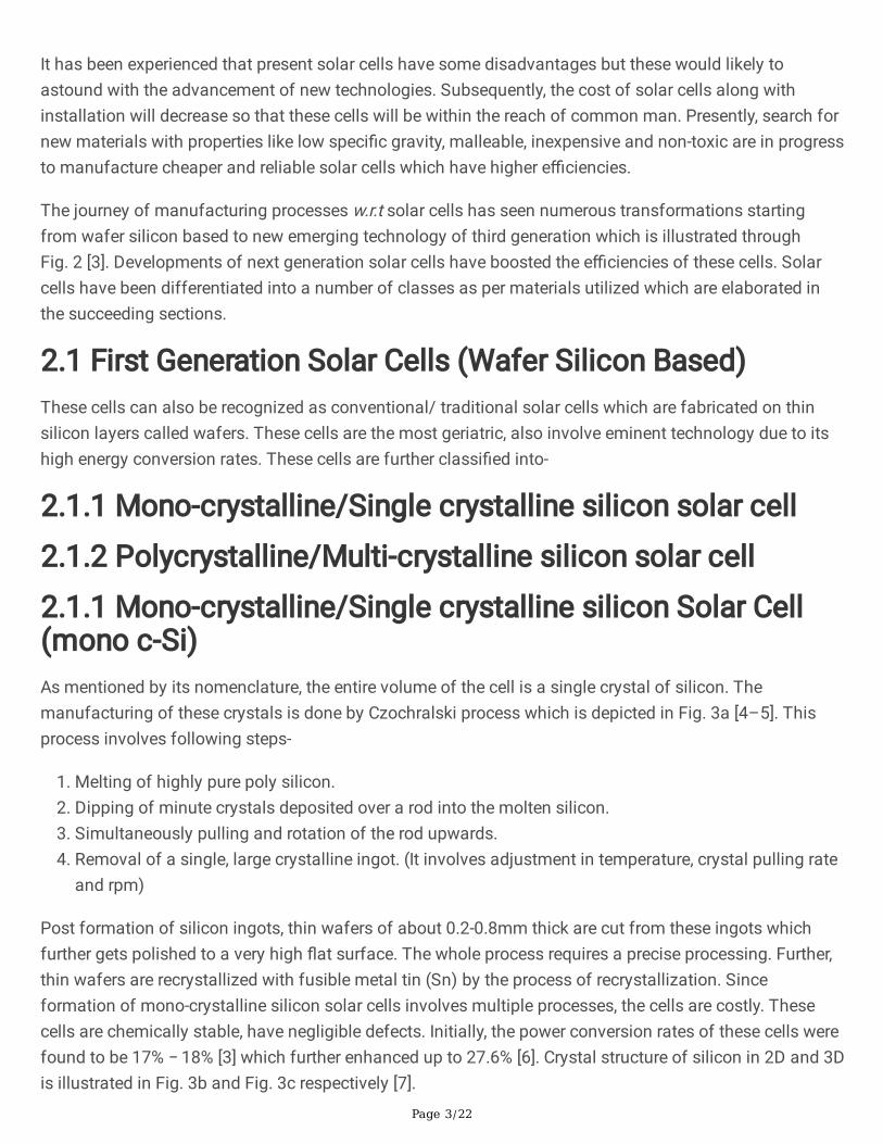
2.1.1 Mono-crystalline/Single crystalline silicon Solar Cell(mono c-Si)As mentioned by its nomenclature, the entire volume of the cell is a single crystal of silicon. Themanufacturing of these crystals is done by Czochralski process which is depicted in Fig. 3a [4–5]. Thisprocess involves following steps-
1. Melting of highly pure poly silicon.2. Dipping of minute crystals deposited over a rod into the molten silicon.3. Simultaneously pulling and rotation of the rod upwards.4. Removal of a single, large crystalline ingot. (It involves adjustment in temperature, crystal pulling rate
and rpm)
Post formation of silicon ingots, thin wafers of about 0.2-0.8mm thick are cut from these ingots whichfurther gets polished to a very high at surface. The whole process requires a precise processing. Further,thin wafers are recrystallized with fusible metal tin (Sn) by the process of recrystallization. Sinceformation of mono-crystalline silicon solar cells involves multiple processes, the cells are costly. Thesecells are chemically stable, have negligible defects. Initially, the power conversion rates of these cells werefound to be 17% − 18% [3] which further enhanced up to 27.6% [6]. Crystal structure of silicon in 2D and 3Dis illustrated in Fig. 3b and Fig. 3c respectively [7].
Page 4/22
Major drawback of these cells is that these cells do not operate eciently whenever the ambienttemperature rises above 25oC. Therefore, an effective air circulation system surrounding the panel must beinstalled for heat exchanging to avoid unnecessary heating. Subsequently, the eciency of these cells isalso increased [8].
2.1.2 Polycrystalline/ Multi-crystalline Silicon Solar Cell(Poly-Si or Mc-Si)Poly/ Multi-crystalline silicon solar cell is usually manufactured by heating trichlorosilane sedimentationover the silicon rods to maximum temperatures. Distinct crystalline congurations are moulded postmolten silicon solidies [5, 9]. Polycrystalline silicon solar cells are comparatively inexpensive to fabricatethan that of mono-crystalline silicon solar panels because of low processing cost, but the former werecomparatively lesser ecient viz 12% − 14% [3] which further enhanced up to 23.2% [6]. Almost 50% of thetotal solar cells manufactured worldwide in 2008 were limited to these cells only. Even today, these cellsare high in demand among various nations. Ribbon Silicon is very good example of these cells.
2.2 Second Generation Solar Cells (Thin Film based)Synthesis of thin lm solar cell involves stacking up of very thin layers of the order of 1 µm (1 micrometer) of light absorbing materials on a substrates of plastic, glass or metals. Whereas the thickness ofsilicon wafers is 300 µm (micro meter). Therefore, it may be appreciated that thickness of these cells isnearly 300 times thinner than the silicon wafers [3]. In addition to lower thickness, these cells arecomparatively exible and attain lower weight than the conventional rst generation cell. For synthesis ofthin lm solar cell, copper based ternary chalcogenides (here chalcogens refer to elements of group16 inthe periodic table) with general formula CuaBXb where B is Tin (Sn), Antimony (Sb), Bismuth (Bi) and X isSelenium (Se), Tellurium (Te), Suphur (S) is intensely used as p-type materials. Copper antimony sulphide(CuSbS2) is abundantly available on earth. Subsequently, cost of this sulphate is very low. CuSbS2 ispreferred to CuInS2 as the former occupies direct band gap of 1.5 eV while the latter sustains 1.02 eV. Also,for nearly equal ionic radii, Antimony is economical to Indium. Presently, hot injection method is indemand for manufacturing nanoplates and nanoparticles of copper antimony sulphide (CuSbS2) withcommensurate optical and structural properties. Subsequently, this method resulted in maintaining shapeand size uniformity.
Thin lm group of solar cells can be listed as mentioned below [10]-
2.2.1 Amorphous silicon cell (a-Si)
2.2.2 Cadmium Telluride cell (CdTe)
2.2.3 Copper Indium Gallium Selenium cell (CIGS)
Page 5/22
2.2.1 Amorphous Silicon Solar Cell (a-Si)Amorphous Silicon i.e. a-Si (a non-crystalline structure) solar cells are fabricated by cladding the dopedsilicon over a exible or a glass substrate. This is done by highly sophisticated Plasma EnhancedChemical Vapour Deposition (PECVD) [7]. The visible light incidented on the uppermost layer of a-Si and apart of incidented light lands on the bottom of cell while rest of the light is reected back. AmorphousSilicon constitutes a band gap of 1.7 eV, comparatively greater than that of c-Si. Schematic representationof chemical bonding in a-Si and a-Si: Hydrogen is illustrated in Fig. 4a and Fig. 4b respectively [7].Schematic stacking of different layers in a typical a-Si cell is illustrated through Fig. 4c [7]. Main demeritof a-Si cells is that their conversion eciencies are almost unstable uctuating from 4–8%. However,these cells can also perform satisfactorily at higher temperatures. Furthermore, these cells are adapted tovariable weather conditions where intensity of sunlight is not optimum. The eciency improvement of a-Sihas seen a leap from 2.4% to 14 % between 1976 and 2020 which is depicted through Table 1 [11–14, 6].
c Schematic arrangement of various lms in a typical amorphous Si solar cell.
Table 1Development of a-Si solar cells & their
conversion eciencies between 1976–2020Sr. No. Eciency (%) Year Ref. No.
1 2.4 1976 11
2 9.3 1986 12
3 11.8 1996 13
4 13.6 2015 14
5 14 2020 6
2.2.2 Cadmium Telluride Solar Cell (CdTe)Though Cadmium (Cd) is a highly toxic element and tellurium is available in scarcity yet CadmiumTelluride (CdTe) is a better selection for advancement of low cost photovoltaic device. Its manufacturingtechnology is inexpensive as well it provides the optimum band gap of approx. 1.45 eV which permits theabsorption of light easily, resulting in increased eciency of solar cell. Since cadmium and telluriumbelong to group 12 and group 16 element of the periodic table respectively, these elements possess highoptical absorption and chemical stability. Crystal structure (zinc blend cubic) of CdTe solar cell isillustrated in Fig. 5a [7]. Schematic illustration of CdTe solar cell with requisite layers of materials isillustrated in Fig. 5b [7]. Subsequently, these elements are the most appropriate for processing thin lmsolar cell [15]. The eciency improvement of CdTe cell has seen a jump from 6% to 22.1 % between 1972[16] and 2020 [6].
b Standard Structure of CdTe/CdS Solar Cell.
Page 6/22
2.2.3 Copper Indium Gallium Di-Selenide Solar Cell (CIGS)Copper (Cu), Indium (In), Gallium (Ga) and Selenium (Se) are the main building blocks of CIGS cells whichrepresents the group 11, group 13, group 13 and group 16 respectively of the periodic table. CIGS hasgeneral molecular formula of [CuInxGa1−xSe2]. Copper Indium di Selenide i.e. x = 1 was initially developedwhich had favourable optical and electrical properties with band gap 1.04 eV. On further investigation, itwas found that its energy level can further be increased to 1.68 eV by replacing indium with gallium [7].However, only a partial replacement of indium with gallium is done to keep the resistivity of material atoptimum level. Therefore, by changing the ratio of quantity of indium to gallium one can tune theforbidden gap between 1.04 eV-1.68 eV as per requirement. Further, CIGS materials have an opticalabsorption coecient of 1015per cm for 1.5 eV. Crystal structure of CIGS is illustrated through Fig. 6a [7].CIGS structure and various layers of described cell is illustrated in the Fig. 6b [8] and Fig. 6c [7]respectively. The eciency improvement of CIGS cell has seen a jump from 4.5% to 23.3 % between 1976[17] and 2020 [6].
c Layer sequence in CIGS Solar Cell.
2.3 Third Generation Solar Cells (New EmergingTechnologies)Third Generation also known as multi-junction solar cells improved electrical conductivity while retainingvery low manufacturing costs. Recent researches are aiming the eciencies of 30–60% with low-pricedmaterials and manufacturing techniques. Types of various third generation cells are as mentioned-
2.3.1 Organic solar cells (OSC)
2.3.2 Quantum dots (QD) solar cells
2.3.3 Concentrated solar cells (CPV)
2.3.4 Transparent solar cells (TSC)
2.3.5 Perovskite solar cells (PSC)
2.3.1 Organic Solar Cells (OSC)Organic solar cells comprise of carbon & hydrogen compounds along with halogens, chalcogens andpnictogens. These cells are manufactured using organic polymers. Organic polymers behave likeconductors by displacing π electrons and adding of sulphur as doping agent e.g. P3HT poly(3-hexylthiophene-2,5-diyl) & PCBM [6, 6]-Phenyl-C61-butyric acid methyl ester behaves as donor andacceptor respectively [18]. Architecture and working of various organic solar cells are as follows-
Page 7/22
Architecture and working:
1. Single Layer
The single layer OSC has a single lm of photosensitive material. This cell’s conguration ops to touchthe standard energy eciencies because of limitations of organic constituents & demand of energy forsplitting of excitons is quite high as depicted in Fig. 7a and 7b [19].
1. Multiple layer or Hetero-Junction
Tang, in 1986, observed materials with lower Ionization Potential (IP/LUMO) effortlessly provide electronswhereas materials with higher Electron Anity (EA/HOMO) receive electrons without any diculty.Subsequently, he discovered a dramatic increase in eciency introducing a donor & an acceptorsimultaneously in one cell and introduced the rst heterojunction photovoltaic cell [19]. In these devices,photocurrent generation process include the following steps-
Formation of excitons (electron-hole pair) followed by absorption of light packets.
Diffusion of excitons towards the junction.
The splitting of excitons into separate holes & electrons.
Transportation and accumulation of holes & electrons at respective electrodes.
Various edices of heterojunction cells are Bi-layer hetero junction, Bulk Heterojunction (BHJ), TandemHeterojunction structures.
i. Bilayer or Planar Heterojunction structure- The bilayer heterojunction solar cell also named as planarOSC consists of two closely connected thin lms of donor & acceptor materiel packed between twoelectrodes as depicted in Fig. 7c [19]. The main drawback of planar OSC is that excitons formed near thejunction ( < ~ 20nm) dissociate only, at larger distances ( > ~ 20nm) w.r.t junction, the electrons and holesproduced is recombined prior reaching donor-acceptor junction because of low mobility and shortdiffusion length. Consequently, the planar heterojunction fail to achieve higher eciency.
To ameliorate the prociency of bilayer organic heterojunction, efforts were made to reduce the lmthickness of photosensitive layer to the order of diffusion length of excitons. However, the same wereresulted in the formation of ultra-thin lm with lower light absorption, subsequently; lesser number ofexcitons was produced as depicted in Fig. 7d [19].
ii. Bulk or Dispersed Heterojunction (BHJ)- The Bulk Heterojunction (BHJ) solar cell also dened asDispersed Heterojunction consists of blended donor-acceptor semiconductor materials as shown in Fig. 7e[19]. Consequent to this arrangement, the excitons can easily dissociate into separate electrons & holesand can be simply diffused to adjoining interface. This conguration has shown much higher PCEs thanthe Bilayer/ Planar Heterojunctions. Normally, both congurations viz small-molecule based bulkHeterojunction & polymer based bulk Heterojunction exhibit highest PCEs. In recent time, researchers aremore enthusiastic in P3HT:PCBM based BHJ OSC [19].
Page 8/22
iii. Tandem Heterojunction- As it is well known that light absorption in single layer, planar heterojunctionand BHJ OSCs are restricted, Tandem Heterojunction cells can absorb energy packets from the shortwavelength zone as well as from the long wavelength zone. Tandem OSCs are well known for its uniquefeature of maximising the solar spectrum absorption. As depicted in Fig. 7f and 7g, Tandem congurationcomprises of two BHJ cells with corresponding photo absorption spectrum, parted by an interconnectinglayer designed to gather charged particles created within the cells. This interconnecting layer results in theadjustment of the quasi-Fermi levels of the bottom & the top cell [19].
Due to Van der Waal bonding, an organic tandem solar cell overcomes the problem of photo-voltage losswhich occurs because of thermalization of hot charge carriers, produced when photons possessing energyhigher than that of band gap are consumed. Consequently, these cells are inexpensive and possess highereciency.
Power conversion rate of organic solar cells has been shooted drastically during recent years. Since thematerials used in these cells are degradable, these cells enjoy smaller life. Consequently, introduction ofthese cells in market is a cumbersome job. The progress in energy conversion rate of organic solar cell hasbeen recorded 18.22% till 2020 [20].
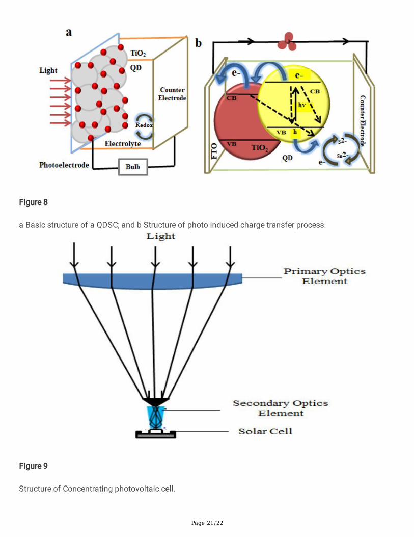
2.3.2 Nano Crystal based or Quantum dots (QDs) basedSolar CellsBurnham and Duggan (1990) used Quantum dots (QDs) for the rst time in solar cells for ebbingundesirable energy losses with involvement of semiconductors of varying energy levels [21]. QDs aresemiconductor nano-particles, usually selected from transition metals of the size of few nanometersequivalent to exciton Bohr radius. Energy levels of QDs can be regulated by altering the dimensions ofparticles which is not feasible with energy level of same semiconductor of larger size. Subsequently, QDsare undoubtly the favourable candidate for multi-junction solar cells because of its exibility in tuning ofband gaps. Formerly, QDs were manufactured using MCVD technique [21]. Later on, these were preparedby wet chemical processing which was an inexpensive and simpler process. Working procedure of aquantum dot solar cell is described through Fig. 8a [22].
Chuang et al. manufactured single-junction PbS Quantum Dot solar cells. Initially, a glass substrate islayered with ITO. Further, a very thin coating of ZnO was coated over ITO coated glass substrate usingspin coating technique followed by deposition of PbS Quantum dots coated with oalic acid using solutionprocessing with tetrabutyl-ammonium iodide (TBAI) and 1,2-ethanedithiol (EDT). At last, gold wasdeposited to the resultant stack as an anode using thermal evaporation technique in vacuum. Photonabsorption by quantum dots results in production of free charged particles which gets collected atrespective electrodes because of internal electric eld generated due to Fermi level orientation of twoelectrodes. The cell with twelve layers of TBAI processed QDs displayed 6% energy eciency. However,substituting the two upper layers of PbS-TbAI with PbS-EDT layers enhanced the energy eciency to 9%because these PbS-EDT layers operated as hole transport and e− blocking layer. Interestingly, QDSCsejects more electrons compared to rst generation cells at the cost of each photon. Production of these
Page 9/22
cells is inexpensive comparing to other photovoltaics because these are processed process from solution.The practical energy eciency of these cells is approximately 2.5% against hypothetical energy eciencywhich is observed to be 45% [7]. Schematic diagram of QDs solar cell is depicted vide Fig. 8b [22]. Theeciency of QD has been upgraded from 1.46–16.6% during the period 2009 [23] − 2020 [6].
2.3.3 Concentrating Solar Cells (CPV)Concentrated PV cell is a cell which is illumined by sunlight that usually converged by employing convexlens or concave mirror. The concentration of sunbeam is vital for actualizing solar cells, exhibiting energyconversion eciencies above 45%, in particular those aiming at 50%. Figure 9 depicts the simplearrangement of a concentrator PV cell [24].Concentrated solar cell was rst come into light in 70s. Thiscell functions on the fundamentals of ray optics. It consists of assembly of big converging mirrors andlenses that intend a surge in the power conversion eciency by converging sunlight that usually fails tofall on the cell surface. Subsequently, a signicant amount of thermal energy is generated. In the domainof solar cells, the concentrated solar cell technology has revealed its boosting persona. Based on thearrangement of lenses and mirrors, these cells are categorized into low, medium & high concentrated PVcells. These cells have exhibited PCE of 38.9 % [3]. Devoid of moving accessories, swift riposte, lowoperating charge and performance at atmospheric temperature are signicant features of these cells.
2.3.4 Transparent Solar Cell (TSC)Earth receives plenty of sunrays but a large portion of its goes in vain and the balance energy is limited tosolar farms and panels of rooftops. Currently, TSCs have attracted the consideration of scientists due totheir increased utilization in society. These cells have been commercialized in many countries while somenations are considering for its utilization in forthcoming years post signicant enhancement of theireciency. TSCs exhibit the capability to yield the energy equal to 40% of energy exploitation of buildingsprovided the availability of TSCs possessing 90% of glass over exterior of each structures/ buildings.Notwithstanding, many developed and developing countries including India are utilizing transparent solarcell technology in automobiles and electronic gadgets. Transparent solar cell consists of an ITO or FTOlm coated on a glass substrate, having 10Ω per square resistance along with a layer thickness ofapproximately 20nm. In addition to intrinsic optical reductions of glass itself, these lms decrease thetransparency of cell by 15% − 20% prior another layer is piled. Till date nearly 80% of transparency isattained [25].
Figure 10 Illustrate the compostions of the TSC [25–26]. An ultra-sensitive layer against UV and NIRradiations is sandwiched between both electrodes which are transparent. The cell includes PBDTT-DPPand PCBM as e- donor and e-acceptor respectively, and both are combined to form a proactive PBDTT-DPP:PCBM layer. 73% and 68% are the maximum and average transmission respectively for thephotoactive material w.r.t visible region (400nm to 650nm). Nonetheless, a UV alongwith NIR regionsturdily engrosses light. To modify the cell, the anode substrate, ITO; coated with PEDOT: PSS ispositioned as the bottommost layer. Since the organic materials are quite sensitive, the electrode needs to
Page 10/22
be positioned at the topmost though this may not sustain the lm sedimentation procedure. To prevailover the scenario, a thin coat of AgNW is layered by spraying technique over the resultant stack. AgNW isstuck to the photosensitive lm in existence of TiO2 sol-gel solution. It needs minute processing [26]. Theeciency of TSC cells has been increased from 4–8.02% within the period from 2012 [26] − 2014 [27].Scientists are now working towards the boosting of the eciency of TSC without compromising itstransparency; the same will be probably achieved in the forthcoming ve years.
2.3.5 Perovskite Based Solar Cell (PSC)LA Perovski, a Russian scientist, discovered Calcium Titanate, CaTiO3, in 1839, having an orthorhombic
crystal symmetry in which larger Ca2+ ions were positioned at the corners while smaller sized Ti4+ werepositioned at the body cubic centre and O2− were situated at face centre in the structure hence was namedperovskite in honour of the Russian scientist. Post this discovery, materials with chemical compositionCDX3 & crystal structure identical to CaTiO3 are identied as perovskites where C, D and X and analogous
to Ca2+, Ti4+ and O2−[7].The perovskites exhibit a highly stable three dimensional network structure. Somecommon perovskites are CsSnI3, FAPbI3, CaTiO3, MAPbI3, MAPbBr3 and MASnI3. The perovskites possessmany magnicent properties viz superconductivity, spintronics & magnetoresistance. Miyasaka et al. werethe rst to use perovskites as a photoactive material in a DSSC [28]. In 2009, they utilized MAPbI3 &MAPbBr3 as photoactive materials, mesoporous TiO2 (m-TiO2) as ETM. LiI/I2 in CH3OCH2CN and LiBr/Br2
in CH3CN had been taken as electrolytes i.r.o MAPbI & MAPbBr respectively for two separate DSSCs.However, they exhibited lower eciencies 3.81% and 3.13% respectively. In addition these cells wereunstable. In 2012, Gratzel et al. were the rst to synthesize MAPbI3 sensitized solar cells using spiro-OMeTAD as HTM in solid form [7]. Surprisingly, this cell exhibited the energy eciency of 9.7% whichprovoked the scientists for perovskite materials that led to the rise to unique type of solar cells termed asperovskite solar cells.
The initial perovskite solar cell used FTO shielded with glass substrates. Further, the substrate wasdeposited with thin lm TiO2 using spin coating method followed by annealing at nearly 500oC for theduration of 20 minutes. The compact layer developed, acted like ETM and constrained the hole activity.Additionally, it behaved like a barrier between FTO and perovskite layer. Thereafter, a layer of m-TiO2 wasencrusted upon compact deposition of TiO2 through the process of doctor blading, followed by sintering
carried out for the duration 45 minutes at 550oC. After that, the resultant compound was layered byemploying MAPbI3, accompanied by heat treatment at 100°C for the duration of 10 minutes. Subsequentlynanocrystal MAPbI3 developed over m-TiO2 coating. Further, a lm of spiro-OMeTAD was coated ontoMAPbI3 using spin coating technique [28]. This lm acted as HTL. At last, the cell was accomplished withnal sedimentation of thin layer of gold (Au) by employing thermal evaporation process. Crystal andSchematic view of Perovskite cell is depicted in Fig. 11a and Fig. 11b respectively [7].
Gratzel et al. in 2013, elaborated an advance procedure for built-up of perovskite lm onto m-TiO2 layerthat gave rise to controlled conguration of perovskite lm. Moreover, this resultant perovskite lm had the
Page 11/22
ability to be adsorbed deeply in m-TiO2 lm which previsiously was not feasible. As a result, PCE of thecell touched the limit of 15% [29]. Over the past few years, Yang et al. exalted the ecacy of ETL byaddition of yttrium (Y) in the compact TiO2 layer that led to increase in cell eciency upto19.3% [30].Ultimately, the energy eciency rate of perovskite cells shoot up to 25.2% from 3.8% [31] till 2020 asshown in Table 2 [32–35, 6]. On the other hand, durability and stability of perovskite cells need notableimprovement. Nonetheless, scientists are highly optimistic to fabricate the perovskite cells of higher powereciencies with very low cost.
Table 2Progress in perovskite cells w.r.t. eciencies during 2001–2020
3. ConclusionAs described in the preceding paragraphs, it has been concluded that recognition of solar cells depend oncost-ecacy, lifespan and eciency. First generation solar cells are undoubtedly the rst choice ofconsumers due to their low cost and best available eciency of 27.6% in spite of various researches onadvanced solar cells of second generation and third generation. Further, cells of second generation arealso promising due to their low cost. In addition, synthesis of these cells is inexpensive than the rstgeneration cells. However, availability of raw material is an issue and lots of efforts are required toimprove their eciencies which are maximum 23.3% till date. It can be seen that while moving from rstgeneration to second generation eciency of solar cell have decreased by 4.3%. Solar cells of thirdgeneration are the most advanced devices. Raw materials used in rst generation are monocrystalline andpolycrystalline Silicon. The materials utilized for second generation cells are CdTe and CIGS. Whileshifting to third generation of solar cells organic materials, perovskites and nano-sized Quantum Dots are
Page 12/22
used. Subsequently, eciency of solar cell has been increased by 11.3% while switching from rstgeneration of solar cells to third generation. Commercialization of cells of third generation is miles awaydue to degradation of the material in short span. However, scientists are putting their best efforts forexploring advance techniques to eradicate the deciency pertaining to commercialization of thirdgeneration solar cells.
DeclarationsFunding statement:
The authors declare that they have no funding available for the publication chargers of open
access. Consider the paper as regular paper.
Conict of Interest:
Authors declare that there is no conict of Interest.
Availability of data and material:
Data used for the results are available in the manuscript in tabular and graphical form.
Compliance with ethical standards:
Not applicable
Consent to participate:
We here give our consent to participate and communicate paper in this journal.
Consent for Publication:
We here give our consent to publish paper in the journal of Silicon, Springer.
Acknowledgment
Research Scholar is thankful to faculty of CDC Department, Department of Electronics andCommunication Engineering NITTTR Chandigarh for their interest in this work and useful comments todraft the nal form of the paper. We would like to thank NITTTR Chandigarh for lab facilities and researchenvironment to carry out this work.
References[1] Rathore, N., Panwar, N.L., Yettou, F., & Gama, A. 2019. A Comprehensive review on different types ofsolar photovoltaic cells and their applications. International J. of Ambient Energy: 1-50,
Page 13/22
https://doi.org/10.1080/01430750.2019.1592774
[2] Solar Cell: Working Principle & Construction. Source: Electrical4U, Oct. 28, 2020,https://www.electrical4u.com/solar-cell.
[3] Sharma, S., Jain, K.K., & Sharma, A.2015.Solar Cells: In Research and Applications-A Review. Mater. Sci.and Appl. 6: 1145-1155, https://doi.org/10.4236/msa.2015.612113
[5] Jiang, L., Cui, S., Sun, P., Wang, Y., & Yang, C. 2020. Comparison of Monocrystalline and PolycrystallineSolar Modules. Proceedings of 5th IEEE Information Technology and Mechatronics EngineeringConference: 341- 344, https://doi.org/10.1109/ITOEC49072.2020.9141722
[6] National Renewable Energy Laboratory, Best research-cell eciencies.https://www.nrel.gov/pv/assets/images/best-research-cell-eciencies.20200406.
[7] Kumar, P., 2017. Handbook of Organic Solar Cells- Device Physics. Processing, Degradation, andPrevention, CRC Press, Taylor & Francis Group, New York. Pp. 1-136, http://lccn.loc.gov/2016008260
[8] Eldin, A.H., Refaey, M., & Farghly, A. 2015. A Review on Photovoltaic Solar Energy Technology and itseciency. Proceedings of 17th International Middle-East Power Sys. Conference (Egypt): 1-8,https://www.academia.edu/15643835
[9] Fujiwara, K., Pan, W., Usami, N., Sawada, K., Tokairin, M., Nose, Y., Nomura, A., Shishido, T., & Nakajima,K. 2016. Growth of structure-controlled polycrystalline silicon ingots for solar cells by casting. ActaMaterialia. 54(12): 3191-3197, https://doi.org/10.1016/j.actamat.2006.03.014
[10] Lee, T.D., & Ebong, A.U. 2017. A review of thin lm solar cell technologies and challenges. Ren. andSus. Energy Reviews. 70: 1286-1297, https://doi.org/10.1016/j.rser.2016.12.028
[11] Carlson, D.E., & Wronski, C.R. 1976. Amorphous silicon solar cell. Appl. Phys. Lett. 28(11): 671- 673,https://doi.org/10.1063/1.88617
[12] Yamazaki, S., Abe, M., Nagayama, S., Shibata, K., Susukida, M., Fukada, T., Kinka, M., Kobayashi, I.,Inushima, T., & Suzuki, K. 1986. Fabrication of the Large-Area Integrated α-Si Solar Cells. MRSProceedings. Cambridge University Press. 70: 487-492, https://doi.org/10.1557/PROC-70-487
[13] Yang, J., Xu, X., Banerjee, A., & Guha, S. 1996. Proceedings of 25th IEEE PVSC. 1041.
[14] Sai, H., Matsui, T., Koida, T., Matsubara, K., Konda, M., Sugiyama, S., Katayama, H., Takeuchi, Y., &Yoshida, I. 2015. Triple-junction thin-lm silicon solar cell fabricated on periodically textured substrate witha stabilized eciency of 13.6%. Appl. Phys. Lett. 106(21): 213902, https://doi.org/10.1063/1.4921794
Page 14/22
[15] Bosio, A., Rosa, G., & Romeo, N. 2018. Past, present and future of the thin lm CdTe/CdS solar cells.Solar Energy. 175: 31-43, https://doi.org/10.1016/j.solener.2018.01.018
[16] Bonnet, D., & Rabenhorst, H. 1972. New results on the development of a thin-lm p-CdTe-n-CdSheterojunction solar cell. Proceedings of 9th IEEE Photovoltaic Specialists Conference: 129-131.
[17] Kazmerski, L.L., White, F.R., & Morgan, G.K. 1976. Thin-lm CuInSe2/CdS heterojunction solar cells.Applied Phys. Lett. 29(4): 268-270, https://doi.org/10.1063/1.89041
[18] Sharma, D., Mehra, R., & Raj B. 2021. Comparative Analysis of Photovoltaic Technologies for HighEciency Solar Cell Design. Superlattices and Microstructures. 153: 106861,https://doi.org/10.1016/j.spmi.2021.106861
[19] Khalil, A., Ahmed, Z., Touati, F., & Masmoudi, M. 2016. Review on organic solar cells. 13th InternationalMulti-Conf. on Sys., Signals & Devices (SSD): 342-353, https://doi.org/10.1109/SSD.2016.7473760
[20] Liu, Q., Jiang, Y., Jin, K., Qin, J., Xu, J., Li, W., Xiong, J., Liu, J., Xiao, Z., Sun, K., Yang, S., Zhang, X., Ding,L. 2020. 18% eciency organic solar cells. Sci. Bull. 65(4): 272-275,https://doi.org/10.1016/j.scib.2020.01.001
[21] Barnham, K.W.J., & Duggan, G. 1990. A new approach to high-eciency multi-band-gap solar cells. J.of App. Phys. 67(7): 3490-3493, https://doi.org/10.1063/1.345339
[22] Baker, D.R., & Kamat, P.V. 2009. Photosensitization of TiO2 nanotubes with CdS quantum dots:Particulate versus tubular support architectures. Adv. Funct. Mater. 19: 805-811,https://doi.org/10.1002/adfm.200801173
[23] Lee, H., Leventis, H.C., Moon, S.J., Chen, P., Ito, S., Haque, S.A., Torres, T., Nuesch, F., Geiger, T.,Zakeeruddin, S.M., Graetzel, M., & Nazeeruddin, M.K. 2009. PbS and CdSquantum dot-sensitized solid-state solar cells: old concepts, new results. Adv. Funct. Mater. 19(17): 2735-2742,https://doi.org/10.1002/adfm.200900081
[24] High eciency concentrated photovoltaic system, http://www.oejournal.org/item/news2020006.html
[25] Husain, A.A.F., Hasan, W.Z.W., Shae, S., Hamidon, M.N., & Pandey, S.S. 2018. A review of transparentsolar photovoltaic technologies. Renew. Sustain. Energy Rev. 94: 779-791,https://doi.org/10.1016/j.rser.2018.06.031
[26] Chen, C.C., Dou, L., Zhu, R., Chung, C.H., Song, T.B., Zheng, Y.B., Hawks, S., Li, G., Weiss, P.S., & Yang, Y.2012. Visibly transparent polymer solar cells produced by solutionprocessing, ACS Nano. 6(8): 7185-7190,https://doi.org/10.1021/nn3029327
[27] Yusoff, A.R.b.M., Lee, S.J., Shneider, F.K., Silva, W.J.d., & Jang, J. 2014. High-performance semi-transparent tandem solar cell of 8.02% conversion eciency withsolution-processed graphene mesh and
Page 15/22
laminated Ag nanowire top electrodes. Adv. Energy Mater. 4(12): 1301989,https://doi.org/10.1002/aenm.201301989
[28] Sharma, D., Mehra, R., & Raj, B. 2020. Recent Advances in Power Systems. In: Gupta, O.H. (Ed.).Materials and Methods for Performance Enhancement of Perovskite Photovoltaic Solar Cells: A Review,EPREC. 699. Pp. 531-542, Springer Nature, Singapore Pte Ltd. https://doi.org/10.1007/978-981-15-7994-3_49
[29] Burschka, J., Pellet, N., Moon, S.J., Baker, R.H., Gao, P., Nazeeruddin, M.K., & Gratzel, M.2013.Sequential deposition as a route to high-performance perovskite-sensitized solar cells. Nature. 499(316):316-320, https://doi.org/10.1038/nature12340
[31] Kojima, A., Teshima, K., Shirai, Y., & Miyasaka, T. 2009. Organometal halide perovskites as visible-lightsensitizers for photovoltaic cells. J. Am. Chem. Soc. 131(17): 6050-6051,https://doi.org/10.1021/ja809598r
[33] Mandadapu, U., Vedanayakam, S.V., & Thyagarajan, K. 2017. Simulation and Analysis of Lead basedPerovskite Solar Cell using SCAPS-1D. Indian J. of Sci. and Tech. 10(11): 1-8,https://doi.org/10.17485/ijst/2017/v11i10/110721
[34] Salah, M.M., Hassan, K.M., Abouelatta, M., & Shaker, A. 2018. A Comparative Study of Different ETMsin Perovskite Solar Cell with Inorganic Copper Iodide as HTM. Optik. 178: 958-963,https://doi.org/10.1016/j.ijleo.2018.10.052
[35] Kaur, P., Pandey, V., & Raj, B. 2020. Comparative Study of Ecient Design, Control and Monitoring ofSolar Power using IoT. Sensor Letter. 18(5): 419-426, https://doi.org/10.1166/sl.2020.4225
Figures
Page 16/22
Figure 1
Voltage / Current Characteristics.
Figure 2
Various solar cell technologies and trending developments.
Page 17/22
Figure 3
a Czochralski Process; b Crystal Structure of Si in 2-D; and c Crystal Structure of Si in 3-D.
Page 18/22
Figure 4
Schematic representation of chemical bonding in a a-Si and b a-Si:H; and c Schematic arrangement ofvarious lms in a typical amorphous Si solar cell.
Page 19/22
Figure 5
a Crystal structure (zinc blend cubic) of CdTe; and b Standard Structure of CdTe/CdS Solar Cell.
Figure 6
Page 20/22
a Crystal structure of CIGS chalcopyrite; b CIGS Solar Cell [8]; and c Layer sequence in CIGS Solar Cell.
Figure 7
a Simplied Energy Diagram of a single Layer OSC & b Single layer OSC. c Simplied Energy Diagram of aBilayer Heterojunction Solar Cell; and d Bilayer Heterojunction Solar Cell. e Bulk Heterojunction; and fTandem Heterojunction Solar Cell. g Simplied Energy Diagram of a Tandem OSC.
Page 21/22
Figure 8
a Basic structure of a QDSC; and b Structure of photo induced charge transfer process.
Figure 9
Structure of Concentrating photovoltaic cell.
Page 22/22
Figure 10
Schematic architecture of a visibly transparent cell [25]
Figure 11
a Perovskite Crystal; & b Schematic presentation of Perovskite solar cell.