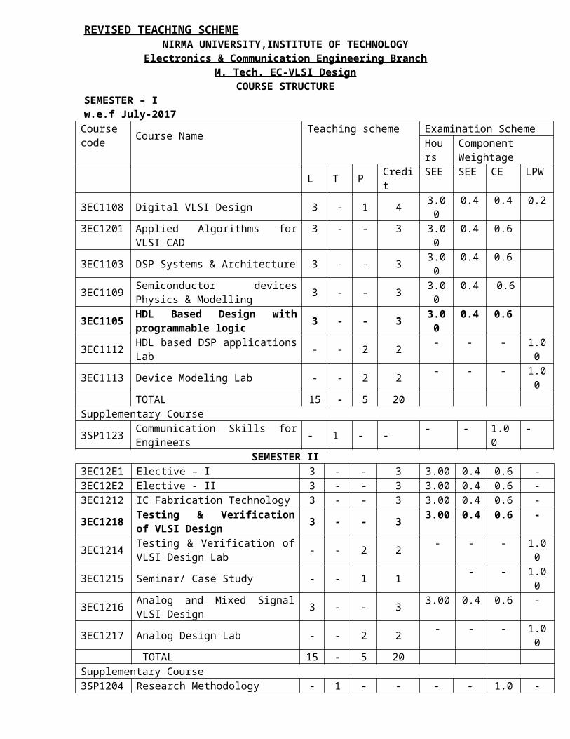
Analog and Mixed Signal VLSI Design 3 - - 3 3.00 0.4 0.6 -
3EC1217 Analog Design Lab - - 2 2 - - - 1.00
TOTAL 15 - 5 20Supplementary Course3SP1204 Research Methodology - 1 - - - - 1.00 -3SP1126 Cyber Security * 1 - - - - - 1.00 -* No sessional exam
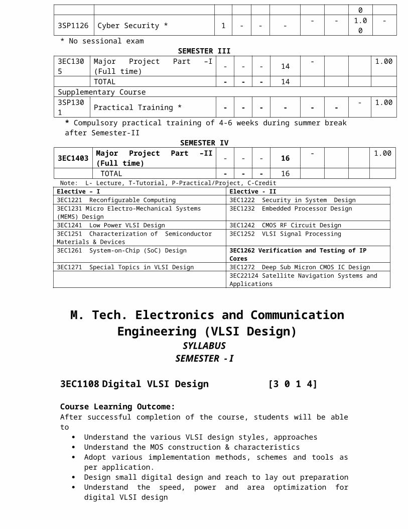
SEMESTER III3EC1305 Major Project Part –I (Full time) - - - 14 - 1.00
TOTAL - - - 14Supplementary Course3SP130 Practical Training * - - - - - - - 1.00
1* Compulsory practical training of 4-6 weeks during summer break after Semester-II
SEMESTER IV3EC1403
Major Project Part –II (Full time) - - - 16 - 1.00
TOTAL - - - 16Note: L- Lecture, T-Tutorial, P-Practical/Project, C-Credit
Elective – I Elective - II3EC1221 Reconfigurable Computing 3EC1222 Security in System Design3EC1231 Micro Electro-Mechanical Systems (MEMS) Design
3EC1232 Embedded Processor Design
3EC1241 Low Power VLSI Design 3EC1242 CMOS RF Circuit Design3EC1251 Characterization of Semiconductor Materials & Devices
3EC1252 VLSI Signal Processing
3EC1261 System-on-Chip (SoC) Design 3EC1262 Verification and Testing of IP Cores3EC1271 Special Topics in VLSI Design 3EC1272 Deep Sub Micron CMOS IC Design
3EC22124 Satellite Navigation Systems and Applications
M. Tech. Electronics and Communication Engineering (VLSI Design)
SYLLABUSSEMESTER - I
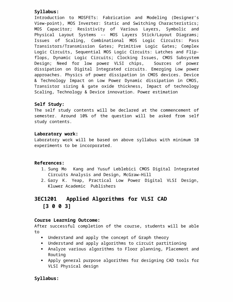
3EC1108 Digital VLSI Design [3 0 1 4]
Course Learning Outcome:After successful completion of the course, students will be able to
Understand the various VLSI design styles, approaches Understand the MOS construction & characteristics Adopt various implementation methods, schemes and tools as per
application. Design small digital design and reach to lay out preparation Understand the speed, power and area optimization for digital VLSI
design
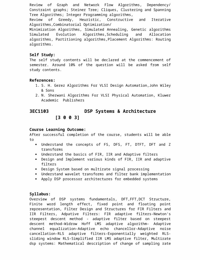
Syllabus:Introduction to MOSFETs: Fabrication and Modeling (Designer’s View-point), MOS Inverter: Static and Switching Characteristics; MOS Capacitor; Resistivity of Various Layers, Symbolic and Physical Layout Systems -- MOS Layers Stick/Layout Diagrams; Issues of Scaling, Combinational MOS Logic Circuits: Pass Transistors/Transmission Gates; Primitive Logic Gates; Complex Logic Circuits, Sequential MOS Logic Circuits: Latches and Flip-flops, Dynamic Logic Circuits; Clocking Issues, CMOS Subsystem Design; Need for low power VLSI chips, Sources of power dissipation on Digital Integrated circuits. Emerging Low power approaches. Physics of power dissipation in CMOS devices. Device & Technology Impact on Low Power Dynamic dissipation in CMOS, Transistor sizing & gate oxide thickness, Impact of technology Scaling, Technology & Device innovation. Power estimation
Self Study:The self study contents will be declared at the commencement of semester. Around 10% of the question will be asked from self study contents.
Laboratory work:
Laboratory work will be based on above syllabus with minimum 10 experiments to be incorporated.
References:1. Sung Mo Kang and Yusuf Leblebici CMOS Digital Integrated Circuits
Analysis and Design, McGraw-Hill2. Gary K. Yeap, Practical Low Power Digital VLSI Design, Kluwer
Academic Publishers
3EC1201 Applied Algorithms for VLSI CAD [3 0 0 3]
Course Learning Outcome:After successful completion of the course, students will be able to
Understand and apply the concept of Graph theory Understand and apply algorithms to circuit partitioning Analyze various algorithms to Floor planning, Placement and Routing Apply general purpose algorithms for designing CAD tools for VLSI
Physical design
Syllabus:Review of Graph and Network Flow Algorithms, Dependency/ Constraint graphs; Steiner Tree; Cliques, Clustering and Spanning Tree Algorithms; Integer Programming algorithms, Review of Greedy, Heuristic, Constructive and Iterative Algorithms,Combinatorial Optimization/ Minimization Algorithms, Simulated Annealing, Genetic algorithms Simulated Evolution Algorithms,Scheduling and Allocation algorithms, Partitioning algorithms,Placement Algorithms: Routing algorithms.
Self Study:The self study contents will be declared at the commencement of semester. Around 10% of the question will be asked from self study contents.
References:1. S. H. Gerez Algorithms For VLSI Design Automation,John Wiley & Sons2. N. Sherwani Algorithms For VLSI Physical Automation, Kluwer Academic
Publishers
3EC1103 DSP Systems & Architecture [3 0 0 3]
Course Learning Outcome:After successful completion of the course, students will be able to
Understand the concepts of FS, DFS, FT, DTFT, DFT and Z transforms Understand the basics of FIR, IIR and Adaptive filters Design and Implement various kinds of FIR, IIR and adaptive filters Design System based on multirate signal processing Understand wavelet transforms and filter bank implementation Apply DSP processor architectures for embedded systems
Syllabus:
Overview of DSP systems fundamentals, DFT,FFT,DCT Structure, Finite word length effect, fixed point and floating point representation, Filter Design and Structures for FIR Filters and IIR Filters, Adpative Filters: FIR adaptive filters-Newton's steepest descent method - adaptive filter based on steepest descent method-Widrow Hoff LMS adaptive algorithm- Adaptive channel equalization-Adaptive echo chancellor-Adaptive noise cancellation-RLS adaptive filters-Exponentially weighted RLS-sliding window RLS-Simplified IIR LMS adaptive filter, Multirate dsp systems: Mathematical description of change of sampling rate - Interpolation and Decimation - continuous time model - Direct digital domain approach - Decimation by an integer factor - Interpolation by an integer factor - Single and multistage realization –CIC Filter- poly phase realization - Application to sub band coding - Wavelet transform and filter bank implementation of wavelet expansion of signals,Programmable DSP architecture: Memory structure and Addressing, Pipelining, VLIW architecture, Superscalar processor, RISC, CISC.
Self Study:The self study contents will be declared at the commencement of semester. Around 10% of the question will be asked from self study contents.
References:1. John G. Proakis , Digital Signal Processing,Prentice Hall of India2. Sanjit Mitra ,Digital Signal Processing, A computer based Approach,
Tata McGraw-Hill3. Peter Pirsch , Architectures for Digital Signal Processing, John Wiley &
Sons
3EC1109 Semiconductor Devices Physics and Modeling [3 0 0 3]
Course Learning Outcome:After successful completion of the course, students will be able to
Apply the basic knowledge of science and mathematics to understand the physics of semiconductor
Apply the fundamentals for understanding of scaled MOS circuits Design MOSFET's of different gate lengths with lambda rules using
TCAD tools for VLSI circuits Understand the different Models of MOSFET's for VLSI circuits Implement the different MOSFET's for VLSI circuit
Syllabus:Basic Semiconductor Physics; Energy Bands and Charge Carriers; MOS Capacitor. MOSFET and Compound Semiconductor FET and modeling, Schottky Barriers and Ohmic Contacts, Bipolar Junction Transistors and modeling, Recent Developments in Microelectronic Devices.
Self Study:The self study contents will be declared at the commencement of semester. Around 10% of the question will be asked from self study contents.
References:1. S. M. Sze, Modern Semiconductor Device Physics,John Wiley & Sons2. D. Nagchoudhuri, Microelectronic Devices, Pearson Education
Course Code 3EC1105L T P C3 - - 3
Course Title HDL Based Design with programmable logic
Course Learning Outcomes (CLO):At the end of the course, students will be able to -
1. Use the Hardware Description Languages like VHDL and Verilog2. Implement the design from specification to net list level3. Design and Implement the digital designs on FPGA in context of
synthesis, device utilization and speed and power optimization
4. Optimize the design using the concepts of simulation, synthesis and Place & Route.
Syllabus: Teaching hours: 45
Introduction to Design Automation, Tools for Design and Analysis of Digital Systems
08
Concepts of Verilog HDL for Behavioural, RTL, Data-flow, Structural and switch level Modeling
15
Designing using using HDLs - VHDL and Verilog 08Programmable Logic Devices, CPLD and FPGA Architectures and Technology,
12
Realization of Digital Design on FPGA 02
Suggested Readings:1. Brown Vranesic, Fundamentals of Digital Logic with Verilog Design.
Tata McGrawHill2. Wyane Wolf, FPGA Based System Design, Pearson3. C. H. Roth, Digital System Design with VHDL, Brookscole
3EC1112 HDL Based DSP Application Lab [0 0 2 2]
Course Learning Outcome:After successful completion of the course, students will be able to
Apply Hardware Description Languages like Verilog and VHDL for higher level applications of digital system design
Effectively use HDL design tools and techniques for implementation of digital system design
Simulate, synthesize and optimize the digital design Design and implement the applications of Digital Signal Processing.
Syllabus:The laboratory work consists of exercise/ assignments based on designing of various applications related to Communication, Digital Signal Processing etc. like Advance multipliers, Direct Digital Synthesizer, dividers, Interface protocols, ALU, memory, Filtering, FFT, Random Number and other function generation algorithms, IP Core Development (System Design). The exercise involves designing of circuits, writing of VHDL/Verilog codes, simulation, synthesis and implementation on FPGA/CPLD boards.
Self Study:The self study contents will be declared at the commencement of semester. Around 10% of the question will be asked from self study contents.
Laboratory work:Laboratory work will be based on above syllabus with minimum 6 experiments to be incorporated. 3EC1113 Device Modeling Lab [0 0 2 2]
Course Learning Outcome:After successful completion of the course, students will be able to
Design, draw and simulate various Semiconductor devices like Diode, nMOS, pMOS, CMOS Process
Understand the impact of material used and device geometry on I/V characteristic of devices
Syllabus:Models for MOS Devices, Parameter Extraction, Noise modelling in CMOS, Drift Diffusion, Lattice Temperature, Energy balance model, 2D and 3D modelling, Mixed mode circuit and device, Device Characterization
Self Study:The self study contents will be declared at the commencement of semester. Around 10% of the question will be asked from self study contents.
Laboratory work: Laboratory work will be based on above syllabus with minimum 6 experiments to be incorporated.
3SP1123 Communication Skills for Engineers [0 1 0 0]
Course Learning Outcome:After successful completion of the course, student will be able to
Learn verbal and non-verbal communication skills Understand types of listening and learn to improve listening skills Learn to draft letters, agenda and minutes of meeting, memo, resume
and job application Learn and develop speaking skills for Group Discussion, Personal
Interview and Seminar Presentation Learn to compose and effectively write Abstract, Research paper and
Dissertation, Summarizing technical material, References and styling, Writing Business Proposal and Report Writing
Syllabus:Communication Skills: Communication cycle, types and flows of Communication, barriers to communication.Non-verbal Communication and Cross-cultural communication Listening Skills: Types of listening, Barriers to effective listening, tips to improve listening skills.
Business Communication: Various types of Letters and format, agenda and minutes of meeting, types of memo and Resume and job application, Email etiquettes Speaking Skills: Group Discussion, Personal Interview, Seminar Presentation Writing Abstract, Research paper and Dissertation, Summarizing technical material References and styling, Writing Business Proposal, Report Writing
Tutorial Work:Tutorial work will be based on above syllabus with minimum 10 tutorials to be incorporated.
References:1. Andrea J Rutherford, Basic Communication Skills for Technology,
Pearson Education2. Shron J. Gerson, Technical Writing Process and Product, Pearson
Education3. Lesiker and Petit, Business Communication, MCGraw Hill4. R.C. Sharma, Krishna Mohan, Business Correspondence and Report
Writing, Tata McGraw Hill
SEMESTER - IIELECTIVE 1
3EC1221 Reconfigurable Computing [3 0 0 3]
Course Learning Outcome:After successful completion of the course, students will be able to
Understand the concept of reconfigurable computing, architectures and types of reconfigurations
Apply the concepts of reconfiguration on the systems design Evaluate the digital systems designed using reconfigurable
architectures for their performance Implement embedded systems of reconfigurable hardware
Syllabus:Computing requirements, Area, Technology scaling, Instructions, Custom Computing Machine, Overview, Comparison of Computing Machines. Fine-grained & Coarse-grained structures, Comparison of different architectures viz. PDSPs, RALU, VLIW, Vector Processors, Memories, Arrays for fast computations, CPLDs, FPGAs, Multi context, Multi FPGA, Partial Reconfigurable Devices, HDL to reconfigurable hardware, Reconfigurable computing systems, Software challenges in System on chip, Testability challenges, Case studies. Modeling and Embedded System Design using FPGA
Self Study:The self study contents will be declared at the commencement of semester. Around 10% of the question will be asked from self study contents.
References:
1. Scott Hauck, Andre Dehon, Reconfigurable Computing, Morgan Kauffman
2. Christophe Bobda, Introduction to Reconfigurable Computing, Springer
3. Maya Gokhale, Paul Ghaham, Reconfigurable Computing, Springer4. IEEE Journal papers on Reconfigurable Architectures, High
Performance Computing Architecture ( HPCA ) Society papers
3EC1231 Micro Electro-Mechanical System (MEMS) Design [3 0 0 3]
Course Learning Outcome:After successful completion of the course, students will be able to
Apply and analyze the concepts advanced Micro/Nano fabrication technologies
Design different techniques and process for microsensor Design application of MEMS in area of optical, modulators, switches,
Self Study:The self study contents will be declared at the commencement of semester. Around 10% of the question will be asked from self study contents.
References:1. G. Kovacs, Micromachined Transducers Sourcebook, McGraw-Hill2. S. Senturia, Microsystem Design, Kluwer Academic Publishers3. M. Madou, Fundamentals of Microfabrication,Chemical Rubber
Company Press4. G. Rebeiz, RF MEMS: Theory, Design and Technology, John Wiley &
Sons5. B. Bouma and G. Tearney, Handbook of Optical Coherence
Tomography, Marcel Dekker Inc
3EC1241 Low Power VLSI Design [3 0 0
3]
Course Learning Outcome:After successful completion of the course, students will be able to
Apply the basic knowledge of science and mathematics to understand the issues related with the power dissipation in VLSI
Apply the fundamentals for understanding of High Speed VLSI from power point of view
Design low power VLSI circuits and to understand the technology associated with it
Understand the different techniques of designing low power VLSI circuits for high density VLSI
Implement the different techniques of low power VLSI Design for different technologies
Syllabus:Need for low power VLSI chips, Sources of power dissipation on Digital Integrated circuits. Emerging Low power approaches. Physics of power dissipation in CMOS devices. Device & Technology Impact on Low Power,Dynamic dissipation in CMOS, Transistor sizing & gate oxide thickness, Impact of technology Scaling, Technology & Device innovation. Power estimation ,Simulation Power analysis: SPICE circuit simulators, gate level logic simulation, capacitive power estimation, static state power, gate level capacitance estimation, architecture level analysis, data correlation analysis in DSP systems. Monte Carlo simulation. Probabilistic power analysis: Random logic signals, probability & frequency, probabilistic power analysis techniques, signal entropy. Low Power Design ,Circuit level: Power consumption in circuits. Flip Flops & Latches design, high capacitance nodes, low power digital cells library Logic level: Gate reorganization, signal gating, logic encoding, state machine encoding, pre-computation logic ,Low power Architecture & Systems: Power & performance management, switching activity reduction, parallel architecture with voltage reduction, flow graph transformation, low power arithmetic components, low power memory design. Low power Clock Distribution : Power dissipation in clock distribution, single driver Vs distributed buffers, Zero skew Vs tolerable skew, chip & package co design of clock network ,Algorithm & architectural level methodologies : Introduction, design flow, Algorithmic level analysis & optimization, Architectural level estimation & synthesis
Self Study:The self study contents will be declared at the commencement of semester. Around 10% of the question will be asked from self study contents.
References:1. Gary K. Yeap, Practical Low Power Digital VLSI Design, Kluwer
Academic Publishers2. Rabaey, Pedram, Low power design methodologies, Kluwer Academic
Course Learning Outcome:After successful completion of the course, students will be able to
Understand the concept of material science and impact on device current voltage characteristic
Understand and apply the knowledge to perform device characterization
Understand the importance of device parasitic and learn techniques to reduce it
Syllabus:Resistivity, four point probe method, resistivity profiling, contact less methods, Carrier and Doping concentration, capacitance measurement, current voltage measurements, optical techniques, Contact resistance and Schottky barrier hight, metal semiconductor contacts, contact resistance measurement techniques, Series resistance channel length and Threshold voltage, Schottky barrier diodes, MOSFETs, Deep level impurities, generation recombination statastics, current measurement and charge measurement, Chemical and physical characterization, Electron beam techniques, ion beam techniques, Xray and gamma ray techniques
Self Study:The self study contents will be declared at the commencement of semester. Around 10% of the question will be asked from self study contents.
References:1. Dieter K.Schroder, Semiconductor Material and Device
characterization, John Wiley & Sons2. S. M. Sze, Modern Semiconductor Device Physics, John Wiley & Sons3. D. Nagchoudhuri, Microelectronic Devices, Pearson Education
3EC1261 System on Chip (SoC) Design [3 0 0 3]
Course Learning Outcome:After successful completion of the course, students will be able to
Understand the various components of system on chip Analyze various system modeling styles Understand various data path architectures and intra-chip
communication issues Analyze partitioning and floor planning algorithms Analyze various modeling and testing languages like System Verilog,
TLM, System C Understand the concept of physical verification and hardware software
co-simulation
Syllabus:System on Chip Technology Challenges, System-level and SoC design methodologies and tools, System On a Chip (SOC) components, System-on-a-chip Peripheral Cores, SoC and interconnect centric Architectures, System level design Representations Virtual platform models, co-simulation and FPGAs for prototyping of HW/SW systems, Intra-chip communication, Architecture selection, Partitioning, scheduling, and communication, Simulation, Task time measurement, Transaction-Level Modeling (TLM), Electronic System-Level (ESL) languages: SystemC Hardware/software
implementation, Performance analysis and optimization, High-Level Synthesis (HLS): allocation, scheduling, binding, resource sharing, Memory & IP Design, pipelining SoC and IP integration, Selfcheck
Self Study:The self study contents will be declared at the commencement of semester. Around 10% of the question will be asked from self study contents.
References:1. D. Black, J. Donovan, SystemC: From the Ground Up, Springer2. D. Gajski, S. Abdi, A. Gerstlauer, G. Schirner, Embedded System
Design: Modeling, Synthesis, Verification, Springer3. T. Noergaard, Embedded Systems Architecture: A Comprehensive
Guide for Engineers and Programmers, Newnes4. Wayone Wolf - Modern VLSI Design: SOC Design, Pearson Education5. Daniel Gajski, Frank Vahid, Sanjiv Narayan, Jie Gong – Specification and
Design of Embedded Systems, Prentice Hall of Indi
3EC1271 Special topics in VLSI Design [3 0 0 3]
Course Learning Outcome:After successful completion of the course, students will be able to
Understand research issues in transistor level design Understand current trends in high performance reliability aware
system level design Understand current trends in testing and verifications
Syllabus:Research issues in CMOS Design, FINFET, Low Power VLSI circuits, Reconfigurable Architecture, Parallel architectures for high performance Systems, Reliability aware System Level Design and Test, Design and implementation of Data converter circuits and applications, Current trends in VLSI design
Self Study:The self study contents will be declared at the commencement of semester. Around 10% of the question will be asked from self study contents.
References:1. IEEE Transaction on VLSI Design2. IEEE Transaction on Circuits and Systems3. Hindawi journal on Reconfigurable Computing4. Other relevant journals
ELECTIVE 2
3EC1222 Security in System Design [3 0 0 3]
Course Learning Outcome:After successful completion of the course, students will be able to
Understand the Cryptography principles Understand the Cryptography analysis in terms of requirements,
design, and implementation Understand Security issues at system design Apply a security concepts to a digital systems project Evaluate and implement the Security requirement from Circuits to
System level
Syllabus:Random Number Generators (Principles of Design), Random Number Generators (Testing and Examples) , Prime Field Arithmetic, Montgomery Multiplication & Exponentiation, Binary Field Arithmetic, Faster Multiplication, Elliptic Curve Cryptography, Efficient Implementation, Hash Functions: Design, Block Ciphers, AES, Basics of Side-channel Analysis, Advanced Side-channel Analysis, Fault Attacks, Countermeasures against SCA, Hiding, Side Channel Countermeasures, Masking, Fault-Attacks and Side-channel Analysis on ECC, Secure Processors Examples
Self Study:The self study contents will be declared at the commencement of semester. Around 10% of the question will be asked from self study contents.
References:1. C. Paar and J. Pelzl, Understanding Cryptography, Springer2. Stefan Mangard, Elisabeth Oswald, Thomas Popp, Power Analysis
Attacks: Revealing the secrets of smartcards, Springer3. Niels Ferguson, Bruce Schneier, and Tadayoshi Kohno, Cryptography
Engineering, John Wiley & Sons4. A.J. Menezes, P.C. van Oorschot, S.A. Vanstone, Handbook of Applied
Cryptography, Chemical Rubber Company Press5. F. Rodriguez-Henriquez, N. A. Saqib, A. Diaz-Perez, and C. K. Koc,
Cryptographic Algorithms on Reconfigurable Hardware, Springer
3EC1232 Embedded Processor Design [3 0 0 3]
Course Learning Outcome:After successful completion of the course, students will be able to
Understand basic architecture of Reduced Instruction Set Computing Apply basic concept of Parallelism and Memory Hierarchy to improve
processor performance Analyze embedded processor peripherals and bus standards Evaluate advanced processor platforms
Syllabus:Review of Processor, Systems and Applications, DSP Implementations, DSP Architectures, ASIP Design Flow, Code Profiling of ASIP Design, Assembly instruction set design, Design of : Micro architecture, ALU, Control path, Memory subsystems, peripheral core, interface to IP cores, Functional acceleration
Self Study:The self study contents will be declared at the commencement of semester. Around 10% of the question will be asked from self study contents.
References:
1. Dake Liu, Embedded DSP Processor Design, Application Specific Instruction set Processors, Morgan Kaufmann
2. Phil Lapsley, Jeff Bier, Amit Shoham, Edward A. Lee, DSP Processor Fundamentals: Architectures and Features, Wiley-IEEE Press
3. Paolo Ienne, Rainer Leupers Customizable Embedded Processors: Design Technologies and Applications, Morgan Kauffman
4. Jean-Pierre Deschamps, Gery J.A. Bioul, Synthesis of Arithmetic Circuits: FPGA, ASIC, John Wiley & Sons
EC1242 CMOS RF Circuit Design [3 0 0 3]
Course Learning Outcome:After successful completion of the course, students will be able to
Understand the concept of RF circuits various receiver architectures Apply the concepts of RF circuit design using active and passive
components Apply the fundamentals of Noise, non linearity and related issues at RF
frequencies Implement circuits like amplifiers, mixers, oscillators, filters, matching
networks etc.
Syllabus:RF systems – basic architectures, Transmission media and reflections, Maximum power transfer, Introduction to MOS.,Parallel RLC tank, Q, Series RLC networks, Matching, Pi match, T match, Interconnects and skin effect, Resistors, capacitors, Inductors design on IC.Noise: Type of Noise, Noise in MOSFETs, Noise Modeling for CMOS, Intrinsic MOS noise parameters, Noise figure. LNA Design: Power match versus noise match, Large signal performance, design examples & Multiplier based mixers. Mixers: Type of Mixers, Mixer Design Examples. RF Power Amplifiers: Class A, AB, B, C amplifiers, Class D, E, F amplifiers, RF Power amplifier design examples.Phase Lock Loops: Linearized PLL models, Phase detectors, charge pumps, Loop filters, PLL design examples.Oscillators and Frequency Synthesizers: Resonators, Negative resistance, Oscillators, Frequency division, Integer-N synthesis, Fractional frequency synthesis, NCO and DDS.Broadband Radio Architectures: GSM radio architectures, CDMA, UMTS radio architectures
Self Study:The self study contents will be declared at the commencement of semester. Around 10% of the question will be asked from self study contents.
References:1. Thomas H. Lee, The Design of CMOS Radio-Frequency Integrated
Circuits, Cambridge University Press2. Behzad Razavi, RF Microelectronics, Prentice Hall of India3. Bosco Lenug , VLSI for Wireless Communication, Prentice Hall of India 4. Robert Caverly, CMOS RF IC Design Principles, Artech House. 5. M. Jamal Deen, Tor A. Fjeldly, CMOS RF Modeling characterization and
application, World Scientific Publication
3EC1252 VLSI Signal Processing [3 0 0 3]
Course Learning Outcome:After successful completion of the course, students will be able to
Understand the concept and requirements of iteration bound Apply basics of pipelining and parallel processing and able design the
system for high speed and low power requirements Perform folding, unfolding and retiming operations on the given
systems Implement various algorithms based on strength reduction of filter,
systolic architectures and fast Fourier transforms Evaluate bit level arithmetic, redundant arithmetic and numerical
strength reduction techniques Syllabus:Introduction to DSP systems, Iteration Bound, Pipelined and parallel processing, Retiming – folding-Unfolding - Algorithmic strength reduction in filters and transforms, Systolic architecture design - fast convolution - Pipelined and parallel recursive and adaptive filters, Scaling and round off noise - Digital lattice filter structures, Bit level arithmetic architecture, Redundant arithmetic, Numerical strength reduction, Synchronous, wave and asynchronous pipe lines, low power design, Programmable digital signal processors.
Self Study:The self study contents will be declared at the commencement of semester. Around 10% of the question will be asked from self study contents.
References:1. Keshab K.Parthi, "VLSI Digital Signal processing systems, Design and
implementation",Wiley2. Uwe, Meyer-Bease,Digital Signal Processing with FPGA , Springer
Course Code 3EC1262Course Title Verification and Testing of IP
CoresCourse Learning Outcomes (CLO):At the end of the course, students will be able to -
1. Analyze the need of specialized verification and testing for FPGA, ASIC, IP Cores and SoC
2. Implement various memory testing methods3. Effectively solve the issues like power, area and time overhead in case
of testing4. Choose the effective methods for analog and mixed mode testing
Syllabus: Teaching hours: 45
Static and Dynamic Timing Analysis 05Logic Level Diagnosis, System Level Diagnosis, BIST with Diagnostic Support
06
Core Based Testing And Test Wrapper, SoC and Embedded System Testing
06
Power Related Reliability Issues, High Speed Low Power Testing Issues
05
Analog and Mixed Signal Testing 04Memory Testing , Memory Fault Modeling, Memory Testing Algorithms, Built-In-Self-Test for Memory, Memory Testing for Nanometer Age
08
Self Checking Design, Built-In-Self-Repair 06I/O Testing, Testing and reliability of FPGAs/ASICs for Space Applications
05
Suggested Readings:1. Malvin A Breuer, Diagnosis and Reliable Design of Digital System,
Computer Science Press2. Laung-Terng Wang et al.,VLSI Test Principals and Architecture:, Morgan
Kaufman3. Stanlay L. Hurst, VLSI Testing : Digital and Mixed Analogue/Digital
Techniques, Institution of Engineering and Technology4. Michael L. Bushnell and Vishwani D. Agrawal Essential of Electronic
Testing for Digital, Memory and Mixed Signal VLSI Circuits, Kluwer Academic Publishers
5. Ashok K Sharma, Semiconductor Memories : Technology, Testing and Reliability, John Wiley & Sons
3EC1272 Deep Submicron CMOS IC Design [3 0 0 3]
Course Learning Outcome:After successful completion of the course, students will be able to
Apply the basic knowledge of science and mathematics to understand the Physics of Deep Sub Micron in MOS Devices
L T P C3 - - 3
Apply the fundamentals for designing scaled MOS digital circuits and cells
Design the Digital MOSFET's of different gate lengths with lambda rules using EDA tools for VLSI circuits at DSM Level
Understand the issues related with DSM IC Deign and fabrication Implement the VLSI circuits with DSM Approach
Syllabus:Deep Sub-micron MOS Transistor Theory & impact of device scaling, Deep Sub-micron Transistor Models, Subthreshold current and ubthreshold swing, Drain Induced Barrier Lowering (DIBL),Punch through, Gate Induced Drain Leakage (GIDL),Deep Sub-micron Noise & Noise Tolerant Designs, Crosstalk, Leakage, Supply Noise & Process Variations, Noise Tolerant Circuit Design Styles (skewed CMOS, noise tolerant domino, layout styles for high noise immunity)CMOS Deep Submicron Fabrication Technology, Silicon Processing Technology Steps ( n-Well CMOS Technology, p-Well, Twin Tub, and Triple Well Technologies), Deep submicron, Fabrication technology, Trench Isolation, Antenna Rules, CMP Rules, Design Margin, Supply Voltage, Temperature, Process Variation, Design Corners, Matching, Delay Tracking, Latch up and Reliability Reliability (Electromigration, Electrostatic discharge (ESD), Electrical overstress (EOS), Self-heating, Hot Carriers), Latchup, Latchup Prevention, Overvoltage, Time-Dependent Dialectric Breakdown (TDDB),Testing for DSM VLSI design,S chmoo Plots, Automatic Test Equipment, Additional JTAG Instructions, Iddq testing of circuits with high intrinsic leakage: delta Iddq, two parameter tests. Idd waveform analysis
Self Study:The self study contents will be declared at the commencement of semester. Around 10% of the question will be asked from self study contents.
References:1. Harry Veendric, Deep Sub micron CMOS ICs, Springer2. Christian Piguet, Low power Electronics Design, Chemical Rubber
Company Press
3EC22124 Satellite Navigation Systems and Applications [ 3 0 0 3] Course Learning Outcome:After successful completion of the course, the students will be able to
understand the principles of satellite navigation systems and compare different navigation systems
learn about the coordinate systems, Navigational signal structure and Vulnerabilities
know the sources of errors with satellite based Navigation systems and solutions
learn about GNSS receiver architecture, chipset design and testing aspects
learn about emerging fields of applications of satellite based navigation system
Syllabus :
Overview of GNSS : A Brief History of Navigation, Evolution of GPS, Development of NAVSTAR GPS, Basic Concepts, GNSS Working Principle, GNSS System Architectute: Space Segment, User Segment, Control Segment. Brief idea of existing Satellite based Navigation System: GPS, GLONASS, Galileo, Compass, QZSS, IRNSS
Coordinate System and Satellite Orbital Dynamics: Geoid, Ellipsoid, Coordinate Systems, Transformation between Cartesian Coordinate Frames, Datums, Conversion between Cartesian and Geodetic Coordinate Frames, Map Projections. GPS coordinate frames, Geodetic and Geo centric coordinate systems, ECEF coordinates, world geodetic 1984 (WGS 84), Kepler’s Laws and Orbital Dynamics, Satellite Orbits, Satellite orbital Parameters, Orbital Perturbations, Ephemeris, Almanac, Satellite Position Determination, GPS Observables, Description of Receiver Independent Exchange Format (RINEX)
Time References and Position Determination: Time Scales: Astronomical and Atomic. Solar and Sidereal Times, Atomic Time, Definition of Time Epoch, Stability Measures of Frequency Sources, Oscillators and their Stability, GPS TimeGNSS Signals and range determination, Trilateration technique, Brief Equations for finding User Position, Pseudorange Measurements in Receiver, User Position Determination from Pseudorange, Concepts of Code Phase Measurements and Carrier Phase Measurements, Differential Positioning
GNSS Satellites and Signal Structure: Introduction to CDMA, PRN Codes, Modulation Types: BPSK, BOC (1,1), BOC(5,2), BOC(m,n), Generation of Codes, GNSS Signals, GNSS Signal Generation, GNSS Signal Characteristics, Signal Power Levels, Navigation Data Structures: Subframes, Frames, Messages, Signal and Message Authentication GNSS Error Sources and Accuracy Issues: Impact of error in pseudorange, Error sources – satellite clock error, receiver clock error, receiver noise, atmospheric error: ionospheric error and tropospheric error, multipath, orbital/ephemeris error, anti spoofing (AS), Selective availability (SA), dilution of precision and estimation of error budget, Ionospheric Error Correction Models (Klobuchar Model, IRNSS Grid Model)GNSS Receivers and its implementation aspects: Signal Components, Receiver Architecture, Signal Conditioning, Signal Acquisition, Acquisition Techniques: Serial Search, Parallel Search, Carrier and Code Tracking Algorithms, Navigation Message Extraction, Positioning Algorithms, Classifications of GNSS receivers, RINEX format, choosing GNSS receivers and selection, GNSS Antennas, Interference Handling, Positioning methods: point positioning, relative positioning, code based relative positioning, carrier based positioning system, processing algorithms, Ne- Quick Model, Tropospheric Corrections, INS Integrated Positioning, GNSS Vulnerabilities : Jamming, Spoofing, Mitigation Techniques and algorithms, Implementation of Acquisition, Tracking and Navigation Processor, testing of GNSS receivers, GNSS Chipset: RFIC and Baseband ASIC and its design aspectsNavigation satellite systems and its Classification: Global systems: GPS, Galileo, GLONASS, Regional systems: COMPASS (Beidou), IRNSS, QZSS, Basic Concept of Differential GPS, Local Area DGPS, Real Time and Post Processing DGPS, Satellite based augmentation system (SBAS-EGNOS, WAAS, MSAS, GAGAN), ground based augmentation system: LAAS, DGPS, Pseudo-lite, Inertial navigation system, integrity of GNSS, e-LORANGNSS Applications: Surveying and Mapping: geodetic control network, GIS mapping, structural deformation survey, construction stack out and grading, coastal engineering survey etc. Navigation: automobile, air craft, maritime,
heavy equipments etc. Tracking: delivery system, precision farming, personal emergencies, fleet management, tracking people etc. Geodynamics: regional and global crustal motion, GIS mapping, ground deformation, mining, research, and other commercial applications; strategic Applications, Geo-fencing etc.Introduction to geodesy: Kinematics, gravity field, size and shape of the Earth; temporal deformations of the Earth., Geodetic control in India, History of geodesy, Geodetic heighten, Terrestrial, celestial Reference, Spherical and ellipsoidal Earth, geodetic datum, datum transformation, Geodetic position determination, coordinate system; coordinate transformations; positioning in 3 dimensions, on the ellipsoid and on a conformal mapping plane. Height systems, Map and Map Projections, Development of global surveying techniques
Self Study:The self study contents will be declared at the commencement of semester. Around 10% of the questions will be asked from self-study contents.
References:1. Bradford W. Parkinson, James J, Spiker Jr. “Global Positioning System:
Theory and Applications” Volume I and Volume II , American Institute of Aeronautics and Astronautics, Inc, Washington
2. Pratap Misra and Per Enge, “Global Positioning System Signals, Mea-surements, and Performance”, Second Edition, Ganga – Jamuna Press, 2006
3. Elliot D. Kaplan & Christopher Hegarty, “Understanding GPS Principles and Applications”, Artech House
4. G S RAO, Global Navigation Satellite Systems, McGraw-Hill publica-tions, New Delhi, 2010
5. B. Hoffman – Wellenhof, H. Liehtenegger and J. Collins, ‘GPS – Theory and Practice’, Springer – Wien, New York (2001).
6. James Ba – Yen Tsui, ‘Fundamentals of GPS receivers – A software ap-proach’, John Wiley & Sons (2001).
Course Learning Outcome:After successful completion of the course, students will be able to
Apply the basic knowledge of science to understand the silicon as a material and its reaction with different gases and chemicals
Apply the fundamentals for understanding the different process involved in the fabrication of VLSI circuits
Understand the fabrication of MOSFET's, BJT and CMOS circuits on silicon wafer
Understand the whole VLSI fabrication flow with multi level metal scheme to solve the power, space and speed problem of circuits on silicon
Develop the skill to implement digital and analog circuits on the different diameter of silicon
Syllabus:
Material properties; Crystal growth; Doping; Diffusion; Oxidation; Epitaxy; Ion Implantation, Deposition of films using CVD, LPCVD and Sputtering Techniques, Wet and Dry Etching and Cleaning; Lithographic Process; Device and Circuit Fabrication, Process Modeling and Simulation.
Self Study:The self study contents will be declared at the commencement of semester. Around 10% of the question will be asked from self study contents.
References:1. S. M. Sze, VLSI Technology, Second Edition, McGraw-Hill2. S. K. Gandhi, VLSI Fabrication Principles, Second Edition, John Wiley &
Sons
Course Code 3EC1218Course Title Testing & Verification of VLSI
Design
Course Learning Outcomes (CLO):At the end of the course, students will be able to -
1. Apply the concepts of testing and verification for VLSI Designs2. Use various EDA tools of testing and verification effectively3. Analyse the various fault models and develop the test patterns for
them.4. Optimize the testing process using Design-for-Test and Built-In-Self-
Test Concepts.
Syllabus: Teaching hours: 45
Verification methods and Advance Tools 04Functional and Formal Verification 04System Verilog – A higher level Verification Language 07Testing Concepts 04Testing Combinatorial and Sequential Circuit 12Random Pattern Testing, Delay Testing, IDDQ Testing 07DFT Techniques, Built-In-Self-Test Techniques 07
Suggested Readings:1. M. L. Bushnell and V. D. Agrawal, Essentials of Electronic Testing for
Digital, Memory and Mixed Signal VLSI Circuits, Kluwer Academic Publishers
2. M. Abramovici, M. A. Breuer and A. D. Friedman, Digital Systems Test-ing and Testable Design, IEEE Press
3. Spear, Chris, Tumbush, Greg, SystemVerilog for Verification-A Guide to Learning the Testbench Language Features, Springer
L T P C3 - - 3
3EC1214 Testing and Verification of VLSI Design Lab [0 0 2 2]
Course Learning Outcome:After successful completion of the course, students will be able to
Develop verification architecture for given design Verify the given design with effective use of simulators Prepare the exhaustive list of possible faults for given design and also
able to prepare necessary test set for them Effectively use the various EDA tools for testing and verifications and
also understand the basic fundamentals involved with them
Syllabus:Functional Verification Tools Bus functional model ( BFM ), Test Bench generation using HDL based simulators, PLI / FLI ,TCL / Tk, Test Pattern Generator, Scan-Chain Insertion, DFT and BIST software Tools, code coverage and functional coverage, Timing Verification.
Self Study:The self study contents will be declared at the commencement of semester. Around 10% of the question will be asked from self study contents.Laboratory work:Laboratory work will be based on above syllabus with minimum 10 experiments to be incorporated.
3EC1215 Seminar /Case Study [0 0 1 1]Course Learning Outcome:After successful completion of the course, students will be able to
Carry out intense study on a specific topic related to current development in their field of specialization
Collect, interpret and analyze the information Compare and evaluate the existing solutions for a specific cases study Develop skills of presentation and report writing Develop a skill to work in a team
A student is required to select advance topic relevant to subject studies. The student should refer and review literature from IEEE and equivalent journals/proceedings, prepare and present report based on this.Each student will be assign at least one case study for each will make a presentation and submit a report based on this.
3EC1216 Analog & Mixed Signal VLSI Design [3 0 0 3] Course Learning Outcome:After successful completion of the course, students will be able to
Understand and Design different Analog circuits for various applications as per the user specifications
Understand and Design different Mixed circuits for various applications as per the user specifications
Understand and Design circuit of Operational amplifier for various applications as per the user specifications
Syllabus:Analog VLSI Design:Analog VLSI issues in CMOS technologies, Basic MOS Models, SPICE Models and frequency dependent parameters, Basic NMOS/CMOS Gain stage, and cascade circuits, Frequency response, stability and Noise issues in amplifiers, CMOS analog blocks: Current Sources and Voltage references, Differential amplifier, OPAMP and OTA design, High performance CMOS op-amps, Non-linear analog blocks: Comparator Design, Charged-pump circuits and Multipliers, Switched capacitor circuits, Analog Interconnects, Analog Testing and Layout Mixed Signal Design:Mixed signal issues in CMOS technologies, Sample-and-Hold Circuits, Analog-to-DigitalConverters; Digital-to-Analog Converters, Sigma-Delta Converters.
Self Study:The self study contents will be declared at the commencement of semester. Around 10% of the question will be asked from self study contents.
References:1. Philip E.Allen, Douglas R.Holberg, CMOS Analog Circuit Design, Oxford2. B. Razavi, Design of Analog CMOS Integrated Circuits, McGraw-Hill
3EC1217 Analog Design Lab [0 0 2 2] Course Learning Outcome:After successful completion of the course, students will be able to
Understand Learn CAD tools for layout design and circuit simulation at transistor level
Design and verify analog circuits Design and verify Mixed signal circuits
Syllabus:Experiments based on Design simulation and Lay out preparation of various analog circuits blocks like current mirror and voltage References ,differential amp, cascade amp, OTA, High Performance and high GB amplifiers, Sigma delta ADC using Tanner EDA tool and Micro wind tool ELDO AMS.
Self Study:The self study contents will be declared at the commencement of semester. Around 10% of the question will be asked from self study contents.
Laboratory work:Laboratory work will be based on above syllabus with minimum 10 experiments to be incorporated. 3SP1204 Research Methodology [0 1 0 0]
Course Learning Outcome: After successful completion of the course, student will be able to
Appreciate the importance of literature survey and problem identification for formulating an effective research topic
Integrate the functionality of Mathematical modeling and Statistical analysis for understanding intricacies of the research work
Prepare research plan inclusive of experimental design Effectively communicate with peer groups and technical diaspora using
technical research papers and thesis or reports
Syllabus:Introduction: Objective of research, motivation in research, types of research, interdisciplinary research, scientific methods of research, criteria of good re-search, characteristics of a good researcher.Defining Research Problem: Art of literature review, user of ICT in effective lit-erature review, formulation of problem, formulation of hypothesis, developing research plan, meaning of research design, types of research design, basic principles of experimental design, selection of relevant variables, validity of experiments.Data Collection and Utilization: Types of data, methods & techniques of data collection, sampling, characteristic of a good sample design, methods used in sampling, sampling errors, tests of hypothesis.Quantitative Methods: Data presentation, statistical analysis and interpreta-tion of data, types of analysis, simple regression analysis, correlation, coeffi-cient of determination (r2), z-test, t-test, ANOVA, Chi-square test, multi-vari-ate analysis of data, multiple regression.Computer Application: Role of computer in research, data organization, soft-ware selection and its applications, solving problems by using scientific soft-ware & tools, sample programmes for analysis of data.Thesis Writing and Presentation: Significance of writing thesis, different types of research writing; conference paper, journal paper, patents, thesis etc., dif-ferent steps in writing thesis, layout of thesis, guidelines for writing good thesis, precautions in writing thesis, presentations skills, defending the thesis.
Tutorial Work:Tutorial work will be based on above syllabus with minimum 10 tutorials to be incorporated.
References:1. C R Kothari, Research Methodology: Methods & Techniques Wishwa
Publication2. D K Bhattacharyya, Research Methodology , Excel Books3. Loraine Blaxter, Christina Hughes and Molcolm Tight, How to Research,
Viva Books Pvt. Ltd.4. Paul Oliver, Writing Your Thesis, Vistaar Pulication5. Pat Cryer, The Research Student’s Guide to Success, Viva Books Pvt.
Ltd.
SEMESTER - III
3EC1305 Major Project: Part – I [0 0 0 14]
Course Learning Outcome:After successful completion of the course, students will be able to
Understand the issues related with the recent trends in the field of engineering and its applications
Formulate the problem definition, analyze and do functional simulation of the same
Design, Implement, test and verify the engineering solution related to problem definition
Compile, Comprehend and Present the work carried out Manage Project
A student is required to carry out elaborated project work. The project may be either design and fabrication work or a simulation and synthesis of a problem/system, develop algorithms and verify the feasibility on a computer. At the end of the semester student will be required to submit a detailed report of literature survey, design problem formulation, analysis, functional simulation and synthesis, work plan and work done and will defend his/her work carried out before examiners.
3SP1301 Practical Training
Course Learning Outcome: After successful completion of the course, student will be able to
explore the preferred field of specialization and develop analytical / hardware / software / experimental skills
manage the technical content and work prepare and present technical report
During practical training of 4-6 weeks, students will learn required software tools/ methodologies, either in industry/research organizations/academic institutions etc or there will be a planned in-house training by our faculty members/experts from other organizations, that will help them in their PG dissertation work.
SEMESTER - IV 3EC1403 Major Project: Part II [0 0 0 16]
Course Learning Outcome:After successful completion of the course, students will be able to
Understand the issues related with the recent trends in the field of engineering and its applications
Formulate the problem definition, analyze and do functional simulation of the same
Design, Implement, test and verify the engineering solution related to problem definition
Compile, Comprehend and Present the work carried out Manage Project
A student is required to carry out elaborated project work. The project may be either design and fabrication work or a simulation and synthesis of a problem/system, develop algorithms and verify the feasibility on a computer. At the end of the semester student will be required to submit a detailed report of literature survey, design problem formulation, analysis, functional simulation and synthesis, work plan and work done and will defend his/her work carried out before examiners.