153
Revision Guide for AMD Family 10h Processors 41322 Publication # 3.92 Revision: March 2012 Issue Date:
Revision Guide forAMD Family 10h
Processors
41322Publication # 3.92 Revision:March 2012Issue Date:
© 2006-2012 Advanced Micro Devices, Inc. All rights reserved.The contents of this document are provided in connection with Advanced Micro Devices,Inc. (“AMD”) products. AMD makes no representations or warranties with respect to theaccuracy or completeness of the contents of this publication and reserves the right to makechanges to specifications and product descriptions at any time without notice. The informa-tion contained herein may be of a preliminary or advance nature and is subject to changewithout notice. No license, whether express, implied, arising by estoppel or otherwise, toany intellectual property rights is granted by this publication. Except as set forth in AMD’sStandard Terms and Conditions of Sale, AMD assumes no liability whatsoever, and dis-claims any express or implied warranty, relating to its products including, but not limitedto, the implied warranty of merchantability, fitness for a particular purpose, or infringementof any intellectual property right.
AMD’s products are not designed, intended, authorized or warranted for use as compo-nents in systems intended for surgical implant into the body, or in other applicationsintended to support or sustain life, or in any other application in which the failure ofAMD’s product could create a situation where personal injury, death, or severe property orenvironmental damage may occur. AMD reserves the right to discontinue or make changesto its products at any time without notice.
Trademarks
AMD, the AMD Arrow logo, AMD Athlon, AMD Opteron, AMD Phenom, AMD Sempron, AMD Turion, and combinations thereof, are trademarks of Advanced Micro Devices, Inc.
HyperTransport is a licensed trademark of the HyperTransport Technology Consortium.
Other product names used in this publication are for identification purposes only and may be trademarks of their respective companies.
Revision History 3
Revision Guide for AMD Family 10h Processors41322 Rev. 3.92 March 2012
Revision History
Date Revision Description
March 2012 3.92 Added errata #721-#722 and #725; Updated Suggested Workaround in erratum #417, due to the overlap in affected silicon revision and workaround of erratum #722.
January 2012 3.90 Added erratum #706.December 2011 3.88 Simplified Tables 28-30; Added erratum #700.October 2011 3.86 Clarified erratum #418; Added erratum #573.August 2011 3.84 Clarified erratum #406; Added errata #625, #643, #669 and #670; Updated
erratum #400 and #610 and MSRC001_0141 OS Visible Work-around MSR1 (OSVW_Status) due to the addition of erratum #669.
February 2011 3.82 Updated Tables 14-17, 20-21 and 24-25 for branding; Updated Processor Identification and F4x164 Fixed Errata Register; Updated embedded processors in Tables 4-6 and updated Table 28; Table 28 no longer has specific columns for Embedded AMD Opteron™ Processors; Added AMD Athlon™ II XL Processor, AMD Athlon™ II XLT Processor and AMD Phenom™ II XLT Processor to Overview, Tables 8 and 28; Updated Table 25; Updated errata #263 and #441; Added errata #550 and #610.
August 2010 3.76 Updated Register References and Mnemonics; Updated Tables 18 and 23; Clarified erratum #361; Added erratum #521.
June 2010 3.74 Added Arithmetic and Logical Operators; Split Table 28 into Tables 28 and 29; Added package ASB2, AMD V-Series Mobile Processor, AMD V-Series Dual-Core Mobile Processor, AMD Athlon™ II Neo Mobile Processor, AMD Athlon™ II Neo Dual-Core Mobile Processor and AMD Turion™ II Neo Dual-Core Mobile Processor to Overview and Tables 11, 13, 22, 23, 29 and 30; Added package S1g4, AMD V-Series Mobile Processor, AMD Athlon™ II Mobile Dual-Core Processor, AMD Turion™ II Dual-Core Mobile Processor, AMD Phenom™ II Dual-Core Mobile Processor, AMD Phenom™ II Triple-Core Mobile Processor and AMD Phenom™ II Quad-Core Mobile Processor to Overview and Tables 10, 13, 18, 19, 29 and 30; Added package C32r1 and AMD Opteron™ 4100 Series Processor to Overview and Tables 8, 13, 20, 21, 28, 30 and erratum #405; Added AMD Sempron™ X2 Processor to Overview and Tables 8, 16 and 28; Corrected erratum #319 marking in Tables 27 and 28; Corrected erratum #327 Fix Plan; Updated erratum #383 Suggested Workaround; Added erratum #419 and #486.
April 2010 3.72 Added AMD Phenom™ II X6 Processor and PH-E0 silicon information to Overview, Tables 8, 16, 17, 26, and 27-30; Updated Table 8; Added errata #438 and #459.
4 Revision History
41322 Rev. 3.92 March 2012Revision Guide for AMD Family 10h Processors
March 2010 3.70 Added AMD Opteron™ 6100 Series Processor, HY-D1 silicon information and G34r1 package information to Overview, Tables 5, 12-13 and 20-30; Corrected marking for errata #351, #355 and #383 in Table 28; Updated Table 8; Updated Potential Effect on System and expanded application of Suggested Workaround to additional processor types for erratum #405; Corrected and clarified erratum #383 Suggested Workaround; Added errata #406, #411, #417, #439-#441 and #443.
January 2010 3.66 Added AMD Athlon™ Processor to Tables 7 and 28; Updated Table 8; Updated Constructing the Processor Name String; Added BL-C3 and DA-C3 silicon information to Tables 8, 26 and 27; Added erratum #383 and updated MSRC001_0140 OS Visible Work-around MSR0 (OSVW_ID_Length) and MSRC001_0141 OS Visible Work-around MSR1 (OSVW_Status) for OSVW[3]; Added errata #408 and #437.
December 2009 3.64 Added AMD Athlon™ II Processor to Overview, Tables 8, 16-17 and 28; Updated Tables 16-17 for branding; Updated MSRC001_0140 OS Visible Work-around MSR0 (OSVW_ID_Length) and Table 26; Removed asterisk for errata #351 in Table 27; Updated erratum #319; Updated and clarified erratum #378 in Description, Suggested Workaround and in Table 28; Updated Suggested Workaround for erratum #384; Added erratum #405; Added errata #414-#415, #418, #420 and #421.
September 2009 3.60 Added AMD Athlon™ II Dual-Core Mobile Processor, AMD Sempron™ Mobile Processor, AMD Turion™ II Dual-Core Mobile Processor, AMD Turion™ II Ultra Dual-Core Mobile Processor and S1g3 package information to Overview, Programming and Displaying the Processor Name String, Tables 9, 13, 18, 19, 28 and 30; Added AMD Athlon™ II X3 Processor, AMD Athlon™ II X4 Processor, and AMD Sempron™ Processor to Overview, Tables 8, and 28; Added BL-C2 and RB-C3 silicon information to Tables 8 and 27; Updated Tables 3, 15-17 and 28; Corrected Tables 26 and 30; Updated erratum #350 Fix Planned; Updated erratum #372. Clarified erratum #400 Suggested Workaround; Added erratum #407.
June 2009 3.52 Corrected Table 4; Updated MSRC001_0140 OS Visible Work-around MSR0 (OSVW_ID_Length) and MSRC001_0141 OS Visible Work-around MSR1 (OSVW_Status); Updated erratum #339; Added errata #396-#400; Updated Documentation Support.
June 2009 3.50 Added HY-D0, Fr6 package and Six-Core AMD Opteron™ Processor information in Overview, Tables 4, 12, 14 and 26-30; Added DA-C2, and AMD Athlon™ II X2 Processor information in Overview, Tables 8 and 16-30; Updated Tables 7 and 17; Updated erratum #372 in Table 28; Updated Suggested Workaround in erratum #389; Added errata #373, #374, #384-#386, #388 and #395.
April 2009 3.46 Updated Programming and Displaying the Processor Name String; Updated Table 17; Added Fr5 (1207) package processors to Tables 3, 14-15 and 30; Updated Table 28 for errata #344 and #354 due to Fr5 (1207) processors; Updated erratum #337; Clarified erratum #382; Added errata #387, #389, #391 and #393.
Date Revision Description
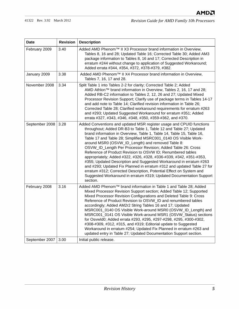
Revision History 5
Revision Guide for AMD Family 10h Processors41322 Rev. 3.92 March 2012
February 2009 3.40 Added AMD Phenom™ II X3 Processor brand information in Overview, Tables 8, 16 and 28; Updated Table 16; Corrected Table 30; Added AM3 package information to Tables 8, 16 and 17; Corrected Description in erratum #244 without change to application of Suggested Workaround; Added errata #344, #354, #372, #378-#379, #382.
January 2009 3.38 Added AMD Phenom™ II X4 Processor brand information in Overview, Tables 7, 16, 17 and 28.
November 2008 3.34 Split Table 1 into Tables 2-2 for clarity; Corrected Table 2; Added AMD Athlon™ brand information in Overview, Tables 2, 16, 17 and 28; Added RB-C2 information to Tables 2, 12, 26 and 27; Updated Mixed Processor Revision Support; Clarify use of package terms in Tables 14-17 and add note to Table 14; Clarified revision information in Table 26; Corrected Table 28; Clarified workaround requirements for erratum #263 and #293; Updated Suggested Workaround for erratum #351; Added errata #327, #343, #346, #348, #350, #359-#362, and #370.
September 2008 3.28 Added Conventions and updated MSR register usage and CPUID functions throughout; Added DR-B3 to Table 1, Table 12 and Table 27; Updated brand information in Overview, Table 1, Table 14, Table 15, Table 16, Table 17 and Table 28; Simplified MSRC001_0140 OS Visible Work-around MSR0 (OSVW_ID_Length) and removed Table 8: OSVW_ID_Length Per Processor Revision; Added Table 26: Cross Reference of Product Revision to OSVW ID; Renumbered tables appropriately; Added #322, #326, #328, #336-#339, #342, #351-#353, #355; Updated Description and Suggested Workaround in erratum #263 and #293; Updated Fix Planned in erratum #312 and updated Table 27 for erratum #312; Corrected Description, Potential Effect on System and Suggested Workaround in erratum #319; Updated Documentation Support section.
February 2008 3.16 Added AMD Phenom™ brand information in Table 1 and Table 28; Added Mixed Processor Revision Support section; Added Table 12; Supported Mixed Processor Revision Configurations and Deleted Table 9: Cross Reference of Product Revision to OSVW_ID and renumbered tables accordingly; Added AM2r2 String Tables 16 and 17; Updated MSRC001_0140 OS Visible Work-around MSR0 (OSVW_ID_Length) and MSRC001_0141 OS Visible Work-around MSR1 (OSVW_Status) sections for OsvwId0; Added errata #293, #295, #297-#298, #295, #300-#302, #308-#309, #312, #315, and #319; Editorial update to Suggested Workaround in erratum #254; Updated Fix Planned in erratum #263 and updated entry in Table 27; Updated Documentation Support section.
September 2007 3.00 Initial public release.
Date Revision Description
6 Overview
Revision Guide for AMD Family 10h Processors 41322 Rev. 3.92 March 2012
Revision Guide for AMD Family 10h Processors
Overview
The purpose of the Revision Guide for AMD Family 10h Processors is to communicate updated product information to designers of computer systems and software developers. This revision guide includes information on the following products:
• AMD Athlon™ Dual-Core Processor• AMD Athlon II Processor• AMD Athlon II Dual-Core Mobile Processor• AMD Athlon II Neo Mobile Processor• AMD Athlon II Neo Dual-Core Mobile Processor• AMD Athlon II X2 Processor• AMD Athlon II XL Processor• AMD Athlon II XLT Processor• AMD Athlon II X3 Processor• AMD Athlon II X4 Processor• Quad-Core AMD Opteron™ Processor• Six-Core AMD Opteron Processor• AMD Opteron 4100 Series Processor• AMD Opteron 6100 Series Processor• Embedded AMD Opteron Processor• AMD Phenom™ Triple-Core Processor• AMD Phenom Quad-Core Processor• AMD Phenom II X2 Processor
Overview 7
Revision Guide for AMD Family 10h Processors41322 Rev. 3.92 March 2012
• AMD Phenom II X3 Processor• AMD Phenom II X4 Processor• AMD Phenom II X6 Processor• AMD Phenom II XLT Processor• AMD Phenom II Dual-Core Mobile Processor• AMD Phenom II Triple-Core Mobile Processor• AMD Phenom II Quad-Core Mobile Processor• AMD Sempron™ Processor• AMD Sempron X2 Processor• AMD Sempron Mobile Processor• AMD Turion™ II Dual-Core Mobile Processor• AMD Turion II Ultra Dual-Core Mobile Processor• AMD Turion II Neo Dual-Core Mobile Processor• AMD V-Series Mobile Processor• AMD V-Series Dual-Core Mobile Processor
This guide consists of these major sections:
• Processor Identification: This section, starting on page 11, shows how to determine the processor revision and workaround requirements, and to construct, program and display the processor name string.
• Product Errata: This section, starting on page 30, provides a detailed description of product errata, including potential effects on system operation and suggested workarounds. An erratum is defined as a deviation from the product’s specification, and as such may cause the behavior of the processor to deviate from the published specifications.
• Documentation Support: This section, starting on page 153, provides a listing of available technical support resources.
Revision Guide PolicyOccasionally, AMD identifies product errata that cause the processor to deviate from published specifications. Descriptions of identified product errata are designed to assist system and software designers in using the processors described in this revision guide. This revision guide may be updated periodically.
8 Conventions
41322 Rev. 3.92 March 2012Revision Guide for AMD Family 10h Processors
Conventions
Numbering• Binary numbers. Binary numbers are indicated by appending a “b” at the end, e.g., 0110b.
• Decimal numbers. Unless specified otherwise, all numbers are decimal. This rule does not apply to the register mnemonics.
• Hexadecimal numbers. Hexadecimal numbers are indicated by appending an “h” to the end, e.g., 45F8h.
• Underscores in numbers. Underscores are used to break up numbers to make them more readable. They do not imply any operation. e.g., 0110_1100b.
• Undefined digit. An undefined digit, in any radix, is notated as a lower case “x”.
Register References and MnemonicsIn order to define errata workarounds it is sometimes necessary to reference processor registers. References to registers in this document use a mnemonic notation consistent with that defined in the BIOS and Kernel Developer’s Guide (BKDG) for AMD Family 10h Processors, order# 31116. Each mnemonic is a concatenation of the register-space indicator and the offset of the register. The mnemonics for the various register spaces are as follows:
• IOXXX: x86-defined input and output address space registers; XXX specifies the byte address of the I/O register in hex (this may be 2 or 3 digits). This space includes the I/O-Space Configuration Address Register (IOCF8) and the I/O-Space Configuration Data Port (IOCFC) to access configuration registers.
• FYxXXX: PCI-defined configuration space; XXX specifies the byte address of the configuration register (this may be 2 or 3 digits) in hex; Y specifies the function number. For example, F3x40 specifies the register at function 3, address 40h. Each processor node includes five functions, 0 through 4.
• FYxXXX_xZZZZZ: Port access through the PCI-defined configuration space; XXX specifies the byte address of the data port configuration register (this may be 2 or 3 digits) in hex; Y specifies the function number; ZZZZZ specifies the port address (this may be 2 to 7 digits) in hex. For example, F2x9C_x1C specifies the port 1Ch register accessed using the data port register at function 2, address 9Ch. Refer to the BIOS and Kernel Developer’s Guide (BKDG) for AMD Family 10h Processors, order# 31116 for access properties.
Conventions 9
Revision Guide for AMD Family 10h Processors41322 Rev. 3.92 March 2012
• APICXXX: APIC memory-mapped registers; XXX is the byte address offset from the base address in hex (this may be 2 or 3 digits). The base address for this space is specified by the APIC Base Address Register (APIC_BAR) at MSR0000_001B.
• CPUID FnXXXX_XXXX_RRR_xYYY: processor capability information returned by the CPUID instruction where the CPUID function is XXXX_XXXX (in hex) and the ECX input is YYY (if specified). When a register is specified by RRR, the reference is to the data returned in that register. For example, CPUID Fn8000_0001_EAX refers to the data in the EAX register after executing CPUID instruction function 8000_0001h.
• MSRXXXX_XXXX: model specific registers; XXXX_XXXX is the MSR number in hex. This space is accessed through x86-defined RDMSR and WRMSR instructions.
Many register references use the notation “[]” to identify a range of registers. For example, F2x[1,0][4C:40] is a shorthand notation for F2x40, F2x44, F2x48, F2x4C, F2x140, F2x144, F2x148, and F2x14C.
Arithmetic and Logical OperatorsIn this document, formulas follow some Verilog conventions as shown in Table 1.
Table 1. Arithmetic and Logic OperatorsOperator Definition
{} Curly brackets are used to indicate a group of bits that are concatenated together. Each set of bits is separated by a comma. E.g., {Addr[3:2], Xlate[3:0]} represents a 6-bit value; the two MSBs are Addr[3:2] and the four LSBs are Xlate[3:0].
| Bitwise OR operator. E.g. (01b | 10b == 11b).
|| Logical OR operator. E.g. (01b || 10b == 1b); logical treats multibit operand as 1 if >=1 and produces a 1-bit result.
& Bitwise AND operator. E.g. (01b & 10b == 00b).
&& Logical AND operator. E.g. (01b && 10b == 1b); logical treats multibit operand as 1 if >=1 and produces a 1-bit result.
^ Bitwise exclusive-OR operator; sometimes used as “raised to the power of” as well, as indicated by the context in which it is used. E.g. (01b ^ 10b == 11b). E.g. (2^2 == 4).
~ Bitwise NOT operator (also known as one’s complement). E.g. (~10b == 01b).
! Logical NOT operator. E.g. (!10b == 0b); logical treats multibit operand as 1 if >=1 and produces a 1-bit result.
== Logical “is equal to” operator.
!= Logical “is not equal to” operator.
<= Less than or equal operator.
>= Greater than or equal operator.
* Arithmetic multiplication operator.
/ Arithmetic division operator.
10 Conventions
41322 Rev. 3.92 March 2012Revision Guide for AMD Family 10h Processors
<< Shift left first operand by the number of bits specified by the 2nd operand. E.g. (01b << 01b == 10b).
>> Shift right first operand by the number of bits specified by the 2nd operand. E.g. (10b >> 01b == 01b).
Table 1. Arithmetic and Logic Operators (Continued)Operator Definition
Processor Identification 11
Revision Guide for AMD Family 10h Processors41322 Rev. 3.92 March 2012
Processor Identification
This section shows how to determine the processor revision, program and display the processor name string, and construct the processor name string.
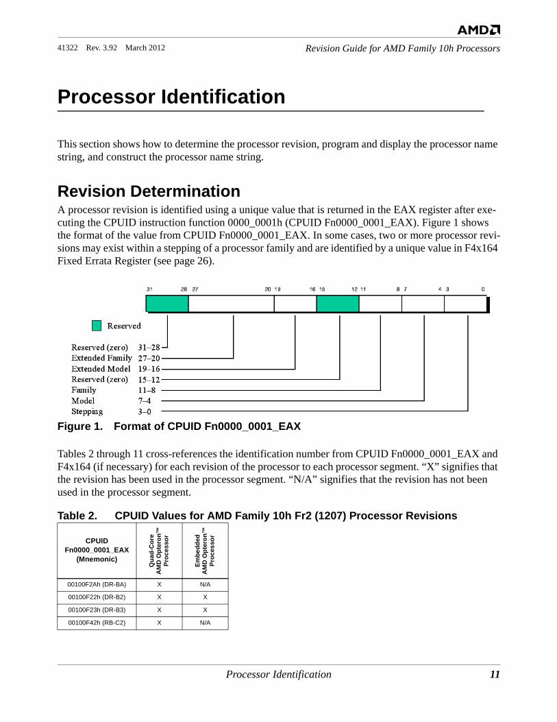
Revision DeterminationA processor revision is identified using a unique value that is returned in the EAX register after exe-cuting the CPUID instruction function 0000_0001h (CPUID Fn0000_0001_EAX). Figure 1 shows the format of the value from CPUID Fn0000_0001_EAX. In some cases, two or more processor revi-sions may exist within a stepping of a processor family and are identified by a unique value in F4x164 Fixed Errata Register (see page 26).
Figure 1. Format of CPUID Fn0000_0001_EAX
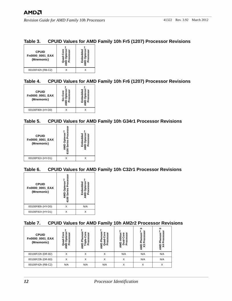
Tables 2 through 11 cross-references the identification number from CPUID Fn0000_0001_EAX and F4x164 (if necessary) for each revision of the processor to each processor segment. “X” signifies that the revision has been used in the processor segment. “N/A” signifies that the revision has not been used in the processor segment.
Table 2. CPUID Values for AMD Family 10h Fr2 (1207) Processor Revisions
CPUID Fn0000_0001_EAX
(Mnemonic)
Qua
d-C
ore
AM
DO
pter
on™
Proc
esso
r
Embe
dded
AM
DO
pter
on™
Proc
esso
r
00100F2Ah (DR-BA) X N/A
00100F22h (DR-B2) X X
00100F23h (DR-B3) X X
00100F42h (RB-C2) X N/A
12 Processor Identification
41322 Rev. 3.92 March 2012Revision Guide for AMD Family 10h Processors
Table 3. CPUID Values for AMD Family 10h Fr5 (1207) Processor Revisions
CPUID Fn0000_0001_EAX
(Mnemonic)Q
uad-
Cor
eA
MD
Opt
eron
™Pr
oces
sor
Embe
dded
AM
DO
pter
on™
Proc
esso
r
00100F42h (RB-C2) X X
Table 4. CPUID Values for AMD Family 10h Fr6 (1207) Processor Revisions
CPUID Fn0000_0001_EAX
(Mnemonic) Six-
Cor
eA
MD
Opt
eron
™Pr
oces
sor
Embe
dded
AM
DO
pter
on™
Proc
esso
r
00100F80h (HY-D0) X X
Table 5. CPUID Values for AMD Family 10h G34r1 Processor Revisions
CPUID Fn0000_0001_EAX
(Mnemonic)
AM
DO
pter
on™
6100
Ser
ies
Proc
esso
r
Embe
dded
AM
DO
pter
on™
Proc
esso
r
00100F91h (HY-D1) X X
Table 6. CPUID Values for AMD Family 10h C32r1 Processor Revisions
CPUID Fn0000_0001_EAX
(Mnemonic)
AM
DO
pter
on™
4100
Ser
ies
Proc
esso
r
Embe
dded
AM
DO
pter
on™
Proc
esso
r
00100F80h (HY-D0) X N/A
00100F81h (HY-D1) X X
Table 7. CPUID Values for AMD Family 10h AM2r2 Processor Revisions
CPUID Fn0000_0001_EAX
(Mnemonic)
Qua
d-C
ore
AM
DO
pter
on™
Proc
esso
r
AM
DPh
enom
™Tr
iple
-Cor
ePr
oces
sor
AM
DPh
enom
™Q
uad-
Cor
ePr
oces
sor
AM
DA
thlo
n™D
ual-C
ore
Proc
esso
r
AM
DPh
enom
™ II
X3 P
roce
ssor
AM
DPh
enom
™ II
X4 P
roce
ssor
00100F22h (DR-B2) X X X N/A N/A N/A
00100F23h (DR-B3) X X X X N/A N/A
00100F42h (RB-C2) N/A N/A N/A X X X
Processor Identification 13
Revision Guide for AMD Family 10h Processors41322 Rev. 3.92 March 2012
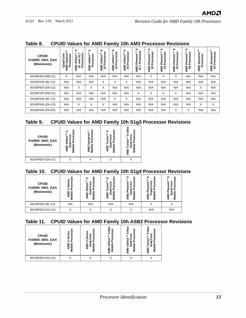
Table 8. CPUID Values for AMD Family 10h AM3 Processor Revisions
CPUID Fn0000_0001_EAX
(Mnemonic)Q
uad-
Cor
eA
MD
Opt
eron
™Pr
oces
sor
AM
DA
thlo
n™ II
XL a
nd X
LTPr
oces
sors
AM
DA
thlo
n™ II
Proc
esso
r
AM
DA
thlo
n™ II
X2 P
roce
ssor
AM
DA
thlo
n™ II
X3 P
roce
ssor
AM
DA
thlo
n™ II
X4 P
roce
ssor
AM
DPh
enom
™ II
XLT
Proc
esso
r
AM
DPh
enom
™ II
X2 P
roce
ssor
AM
DPh
enom
™ II
X3 P
roce
ssor
AM
DPh
enom
™ II
X4 P
roce
ssor
AM
DPh
enom
™ II
X6 P
roce
ssor
AM
DSe
mpr
on™
Proc
esso
r
AM
DSe
mpr
on™
X2 P
roce
ssor
00100F42h (RB-C2) X N/A N/A N/A N/A N/A N/A X X X N/A N/A N/A
00100F52h (BL-C2) N/A N/A N/A X X X N/A N/A N/A N/A N/A N/A N/A
00100F62h (DA-C2) N/A X X X N/A N/A N/A N/A N/A N/A N/A X N/A
00100F43h (RB-C3) N/A N/A N/A N/A N/A N/A X X X X N/A N/A N/A
00100F53h (BL-C3) N/A N/A N/A N/A X X N/A N/A N/A N/A N/A N/A N/A
00100F63h (DA-C3) N/A X X X N/A N/A N/A N/A N/A N/A N/A X X
00100FA0h (PH-E0) N/A N/A N/A N/A N/A N/A N/A N/A N/A X X N/A N/A
Table 9. CPUID Values for AMD Family 10h S1g3 Processor Revisions
CPUID Fn0000_0001_EAX
(Mnemonic)
AM
DA
thlo
n™ II
Dua
l-Cor
eM
obile
Pro
cess
or
AM
DSe
mpr
on™
Mob
ile P
roce
ssor
AM
DTu
rion™
IID
ual-C
ore
Mob
ile P
roce
ssor
AM
DTu
rion™
II U
ltra
Dua
l-Cor
eM
obile
Pro
cess
or
00100F62h (DA-C2) X X X X
Table 10. CPUID Values for AMD Family 10h S1g4 Processor Revisions
CPUID Fn0000_0001_EAX
(Mnemonic)
AM
D V
-Ser
ies
Mob
ile P
roce
ssor
AM
DA
thlo
n™ II
Dua
l-Cor
eM
obile
Pro
cess
or
AM
DTu
rion™
IID
ual-C
ore
Mob
ile P
roce
ssor
AM
DPh
enom
™ II
Dua
l-Cor
eM
obile
Pro
cess
or
AM
DPh
enom
™ II
Trip
le-C
ore
Mob
ile P
roce
ssor
AM
DPh
enom
™ II
Qua
d-C
ore
Mob
ile P
roce
ssor
00100F53h (BL-C3) N/A N/A N/A N/A X X
00100F63h (DA-C3) X X X X N/A N/A
Table 11. CPUID Values for AMD Family 10h ASB2 Processor Revisions
CPUID Fn0000_0001_EAX
(Mnemonic)
AM
D V
-Ser
ies
Mob
ile P
roce
ssor
AM
D V
-Ser
ies
Dua
l-Cor
eM
obile
Pro
cess
or
AM
DA
thlo
n™ II
Neo
Mob
ile P
roce
ssor
AM
DA
thlo
n™ II
Neo
Dua
l-Cor
eM
obile
Pro
cess
or
AM
DTu
rion™
II N
eoD
ual-C
ore
Mob
ile P
roce
ssor
00100F63h (DA-C3) X X X X X
14 Processor Identification
41322 Rev. 3.92 March 2012Revision Guide for AMD Family 10h Processors
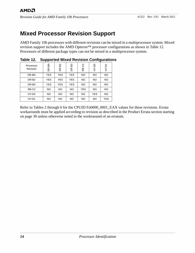
Mixed Processor Revision SupportAMD Family 10h processors with different revisions can be mixed in a multiprocessor system. Mixed revision support includes the AMD Opteron™ processor configurations as shown in Table 12. Processors of different package types can not be mixed in a multiprocessor system.
Refer to Tables 2 through 6 for the CPUID Fn0000_0001_EAX values for these revisions. Errata workarounds must be applied according to revision as described in the Product Errata section starting on page 30 unless otherwise noted in the workraound of an erratum.
Table 12. Supported Mixed Revision ConfigurationsProcessor Revision
DR
-BA
DR
-B2
DR
-B3
RB
-C2
HY-
D0
HY-
D1
DR-BA YES YES YES NO NO NO
DR-B2 YES YES YES NO NO NO
DR-B3 YES YES YES NO NO NO
RB-C2 NO NO NO YES NO NO
HY-D0 NO NO NO NO YES NO
HY-D1 NO NO NO NO NO YES
Processor Identification 15
Revision Guide for AMD Family 10h Processors41322 Rev. 3.92 March 2012
Programming and Displaying the Processor Name StringThis section, intended for BIOS programmers, describes how to program and display the 48-character processor name string that is returned by CPUID Fn8000_000[4:2]. The hardware or cold reset value of the processor name string is 48 ASCII NUL characters, so the BIOS must program the processor name string before any general purpose application or operating system software uses the extended functions that read the name string. It is common practice for the BIOS to display the processor name string and model number whenever it displays processor information during boot up.Note: Motherboards that do not program the proper processor name string and model number will not pass
AMD validation and will not be posted on the AMD Recommended Motherboard Web site.
The name string must be ASCII NUL terminated and the 48-character maximum includes that NUL character.
The processor name string is programmed by MSR writes to the six MSR addresses covered by the range MSRC001_00[35:30]h. Refer to the BIOS and Kernel Developer’s Guide (BKDG) for AMD Family 10h Processors, order# 31116, for the format of how the 48-character processor name string maps to the 48 bytes contained in the six 64-bit registers of MSRC001_00[35:30].
The processor name string is read by CPUID reads to a range of CPUID functions covered by CPUID Fn8000_000[4:2]. Refer to CPUID Fn8000_000[4:2] in the BIOS and Kernel Developer’s Guide (BKDG) for AMD Family 10h Processors, order# 31116, for the 48-character processor name string mapping to the 48 bytes contained in the twelve 32-bit registers of CPUID Fn8000_000[4:2].
Constructing the Processor Name StringThis section describes how to construct the processor name string. BIOS uses the following fields to create the name string:
• BrandId[15:0] is from CPUID Fn8000_0001_EBX[15:0].• String1[3:0] is defined to be BrandID[14:11]. This field is an index to a string value used to
create the processor name string. The definitions of the String1 values are provided in Tables 14, 16, 18, 20, 22 and 24.
• String2[3:0] is defined to be BrandID[3:0]. This field is an index to a string value used to create the processor name string. The definitions of the String2 values are provided in Tables 15, 17, 19, 21, 23 and 25.
• PartialModel[6:0] is defined to be BrandID[10:4]. This field is normally used to create some or all of the model number in the name string. This field represents a number which should be converted to ASCII for display. This field may be decremented by one before use.
• Pg[0] is defined to be BrandID[15]. This field is used to index the appropriate page for the tables.
16 Processor Identification
41322 Rev. 3.92 March 2012Revision Guide for AMD Family 10h Processors
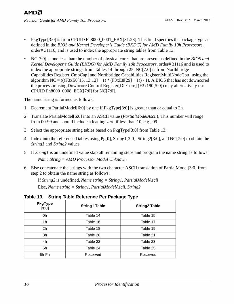
• PkgType[3:0] is from CPUID Fn8000_0001_EBX[31:28]. This field specifies the package type as defined in the BIOS and Kernel Developer’s Guide (BKDG) for AMD Family 10h Processors, order# 31116, and is used to index the appropriate string tables from Table 13.
• NC[7:0] is one less than the number of physical cores that are present as defined in the BIOS and Kernel Developer’s Guide (BKDG) for AMD Family 10h Processors, order# 31116 and is used to index the appropriate strings from Tables 14 through 25. NC[7:0] is from Northbridge Capabilities Register[CmpCap] and Northbridge Capabilities Register[MultiNodeCpu] using the algorithm NC = (((F3xE8[15, 13:12] + 1) * (F3xE8[29] + 1)) - 1). A BIOS that has not downcored the processor using Downcore Control Register[DisCore] (F3x190[5:0]) may alternatively use CPUID Fn8000_0008_ECX[7:0] for NC[7:0].
The name string is formed as follows:
1. Decrement PartialModel[6:0] by one if PkgType[3:0] is greater than or equal to 2h.
2. Translate PartialModel[6:0] into an ASCII value (PartialModelAscii). This number will range from 00-99 and should include a leading zero if less than 10, e.g., 09.
3. Select the appropriate string tables based on PkgType[3:0] from Table 13.
4. Index into the referenced tables using Pg[0], String1[3:0], String2[3:0], and NC[7:0] to obtain the String1 and String2 values.
5. If String1 is an undefined value skip all remaining steps and program the name string as follows:Name String = AMD Processor Model Unknown
6. Else concatenate the strings with the two character ASCII translation of PartialModel[3:0] from step 2 to obtain the name string as follows:
If String2 is undefined, Name string = String1, PartialModelAsciiElse, Name string = String1, PartialModelAscii, String2
Table 13. String Table Reference Per Package TypePkgType
[3:0] String1 Table String2 Table
0h Table 14 Table 15
1h Table 16 Table 17
2h Table 18 Table 19
3h Table 20 Table 21
4h Table 22 Table 23
5h Table 24 Table 25
6h-Fh Reserved Reserved
Processor Identification 17
Revision Guide for AMD Family 10h Processors41322 Rev. 3.92 March 2012
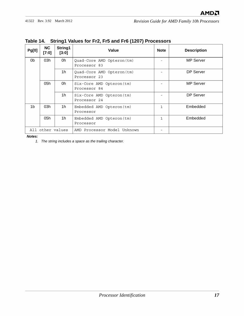
Table 14. String1 Values for Fr2, Fr5 and Fr6 (1207) Processors
Pg[0] NC[7:0]
String1[3:0] Value Note Description
0b 03h 0h Quad-Core AMD Opteron(tm) Processor 83
- MP Server
1h Quad-Core AMD Opteron(tm) Processor 23
- DP Server
05h 0h Six-Core AMD Opteron(tm) Processor 84
- MP Server
1h Six-Core AMD Opteron(tm) Processor 24
- DP Server
1b 03h 1h Embedded AMD Opteron(tm) Processor
1 Embedded
05h 1h Embedded AMD Opteron(tm) Processor
1 Embedded
All other values AMD Processor Model Unknown -
Notes:1. The string includes a space as the trailing character.
18 Processor Identification
41322 Rev. 3.92 March 2012Revision Guide for AMD Family 10h Processors
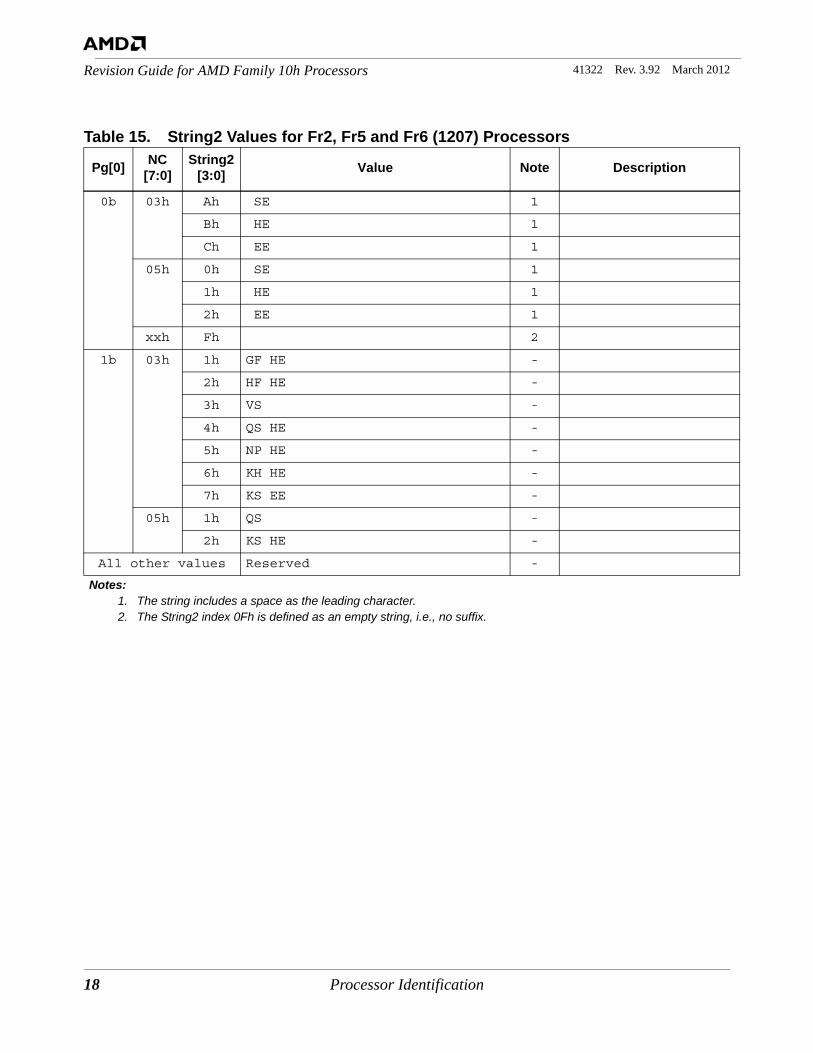
Table 15. String2 Values for Fr2, Fr5 and Fr6 (1207) Processors
Pg[0] NC[7:0]
String2[3:0] Value Note Description
0b 03h Ah SE 1
Bh HE 1
Ch EE 1
05h 0h SE 1
1h HE 1
2h EE 1
xxh Fh 2
1b 03h 1h GF HE -
2h HF HE -
3h VS -
4h QS HE -
5h NP HE -
6h KH HE -
7h KS EE -
05h 1h QS -
2h KS HE -
All other values Reserved -
Notes:1. The string includes a space as the leading character.2. The String2 index 0Fh is defined as an empty string, i.e., no suffix.
Processor Identification 19
Revision Guide for AMD Family 10h Processors41322 Rev. 3.92 March 2012
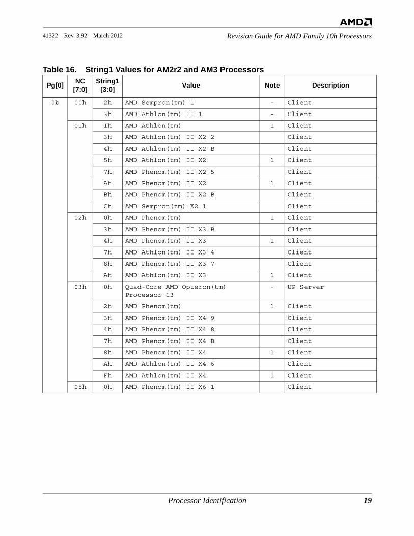
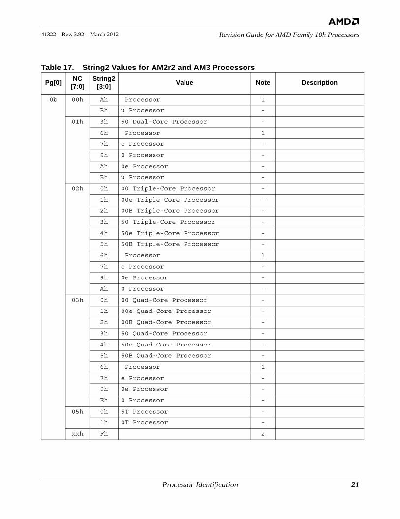
Table 16. String1 Values for AM2r2 and AM3 Processors
Pg[0] NC[7:0]
String1[3:0] Value Note Description
0b 00h 2h AMD Sempron(tm) 1 - Client
3h AMD Athlon(tm) II 1 - Client
01h 1h AMD Athlon(tm) 1 Client
3h AMD Athlon(tm) II X2 2 Client
4h AMD Athlon(tm) II X2 B Client
5h AMD Athlon(tm) II X2 1 Client
7h AMD Phenom(tm) II X2 5 Client
Ah AMD Phenom(tm) II X2 1 Client
Bh AMD Phenom(tm) II X2 B Client
Ch AMD Sempron(tm) X2 1 Client
02h 0h AMD Phenom(tm) 1 Client
3h AMD Phenom(tm) II X3 B Client
4h AMD Phenom(tm) II X3 1 Client
7h AMD Athlon(tm) II X3 4 Client
8h AMD Phenom(tm) II X3 7 Client
Ah AMD Athlon(tm) II X3 1 Client
03h 0h Quad-Core AMD Opteron(tm) Processor 13
- UP Server
2h AMD Phenom(tm) 1 Client
3h AMD Phenom(tm) II X4 9 Client
4h AMD Phenom(tm) II X4 8 Client
7h AMD Phenom(tm) II X4 B Client
8h AMD Phenom(tm) II X4 1 Client
Ah AMD Athlon(tm) II X4 6 Client
Fh AMD Athlon(tm) II X4 1 Client
05h 0h AMD Phenom(tm) II X6 1 Client
20 Processor Identification
41322 Rev. 3.92 March 2012Revision Guide for AMD Family 10h Processors
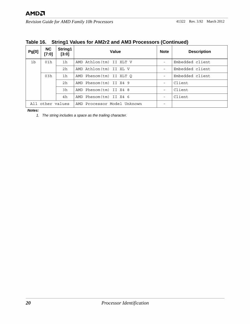
1b 01h 1h AMD Athlon(tm) II XLT V - Embedded client
2h AMD Athlon(tm) II XL V - Embedded client
03h 1h AMD Phenom(tm) II XLT Q - Embedded client
2h AMD Phenom(tm) II X4 9 - Client
3h AMD Phenom(tm) II X4 8 - Client
4h AMD Phenom(tm) II X4 6 - Client
All other values AMD Processor Model Unknown -
Notes:1. The string includes a space as the trailing character.
Table 16. String1 Values for AM2r2 and AM3 Processors (Continued)
Pg[0] NC[7:0]
String1[3:0] Value Note Description
Processor Identification 21
Revision Guide for AMD Family 10h Processors41322 Rev. 3.92 March 2012
Table 17. String2 Values for AM2r2 and AM3 Processors
Pg[0] NC[7:0]
String2[3:0] Value Note Description
0b 00h Ah Processor 1
Bh u Processor -
01h 3h 50 Dual-Core Processor -
6h Processor 1
7h e Processor -
9h 0 Processor -
Ah 0e Processor -
Bh u Processor -
02h 0h 00 Triple-Core Processor -
1h 00e Triple-Core Processor -
2h 00B Triple-Core Processor -
3h 50 Triple-Core Processor -
4h 50e Triple-Core Processor -
5h 50B Triple-Core Processor -
6h Processor 1
7h e Processor -
9h 0e Processor -
Ah 0 Processor -
03h 0h 00 Quad-Core Processor -
1h 00e Quad-Core Processor -
2h 00B Quad-Core Processor -
3h 50 Quad-Core Processor -
4h 50e Quad-Core Processor -
5h 50B Quad-Core Processor -
6h Processor 1
7h e Processor -
9h 0e Processor -
Eh 0 Processor -
05h 0h 5T Processor -
1h 0T Processor -
xxh Fh 2
22 Processor Identification
41322 Rev. 3.92 March 2012Revision Guide for AMD Family 10h Processors
1b 01h 1h L Processor -
2h C Processor -
03h 1h L Processor -
4h T Processor -
All other values Reserved -
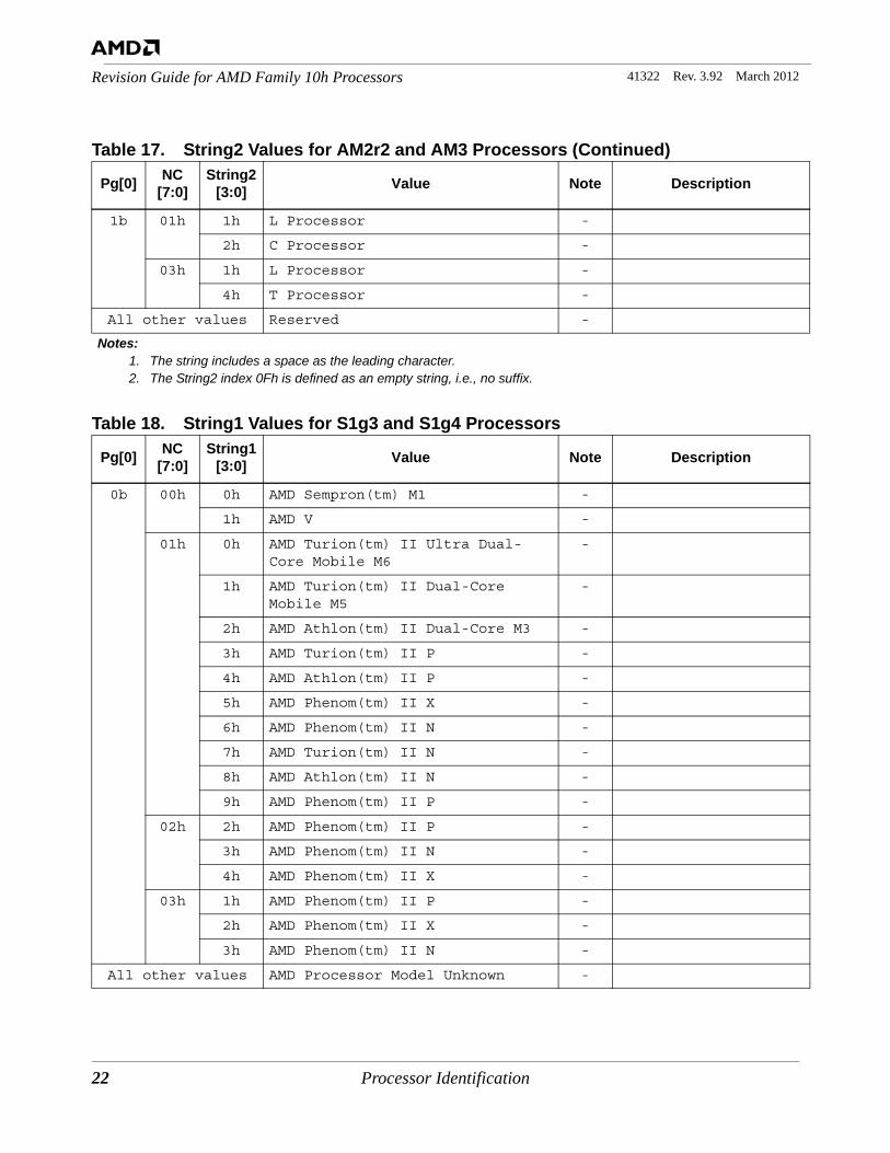
Notes:1. The string includes a space as the leading character.2. The String2 index 0Fh is defined as an empty string, i.e., no suffix.
Table 18. String1 Values for S1g3 and S1g4 Processors
Pg[0] NC[7:0]
String1[3:0] Value Note Description
0b 00h 0h AMD Sempron(tm) M1 -
1h AMD V -
01h 0h AMD Turion(tm) II Ultra Dual-Core Mobile M6
-
1h AMD Turion(tm) II Dual-Core Mobile M5
-
2h AMD Athlon(tm) II Dual-Core M3 -
3h AMD Turion(tm) II P -
4h AMD Athlon(tm) II P -
5h AMD Phenom(tm) II X -
6h AMD Phenom(tm) II N -
7h AMD Turion(tm) II N -
8h AMD Athlon(tm) II N -
9h AMD Phenom(tm) II P -
02h 2h AMD Phenom(tm) II P -
3h AMD Phenom(tm) II N -
4h AMD Phenom(tm) II X -
03h 1h AMD Phenom(tm) II P -
2h AMD Phenom(tm) II X -
3h AMD Phenom(tm) II N -
All other values AMD Processor Model Unknown -
Table 17. String2 Values for AM2r2 and AM3 Processors (Continued)
Pg[0] NC[7:0]
String2[3:0] Value Note Description
Processor Identification 23
Revision Guide for AMD Family 10h Processors41322 Rev. 3.92 March 2012
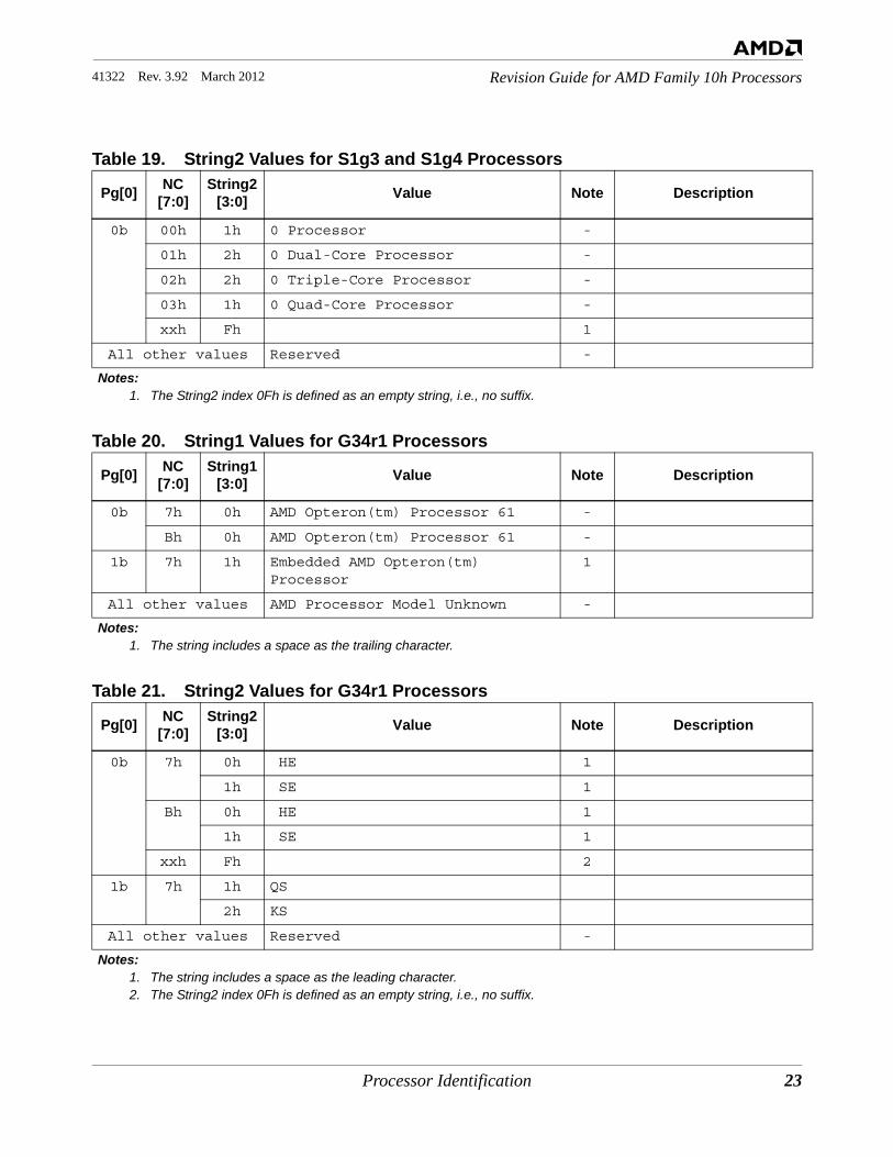
Table 19. String2 Values for S1g3 and S1g4 Processors
Pg[0] NC[7:0]
String2[3:0] Value Note Description
0b 00h 1h 0 Processor -
01h 2h 0 Dual-Core Processor -
02h 2h 0 Triple-Core Processor -
03h 1h 0 Quad-Core Processor -
xxh Fh 1
All other values Reserved -
Notes:1. The String2 index 0Fh is defined as an empty string, i.e., no suffix.
Table 20. String1 Values for G34r1 Processors
Pg[0] NC[7:0]
String1[3:0] Value Note Description
0b 7h 0h AMD Opteron(tm) Processor 61 -
Bh 0h AMD Opteron(tm) Processor 61 -
1b 7h 1h Embedded AMD Opteron(tm) Processor
1
All other values AMD Processor Model Unknown -
Notes:1. The string includes a space as the trailing character.
Table 21. String2 Values for G34r1 Processors
Pg[0] NC[7:0]
String2[3:0] Value Note Description
0b 7h 0h HE 1
1h SE 1
Bh 0h HE 1
1h SE 1
xxh Fh 2
1b 7h 1h QS
2h KS
All other values Reserved -
Notes:1. The string includes a space as the leading character.2. The String2 index 0Fh is defined as an empty string, i.e., no suffix.
24 Processor Identification
41322 Rev. 3.92 March 2012Revision Guide for AMD Family 10h Processors
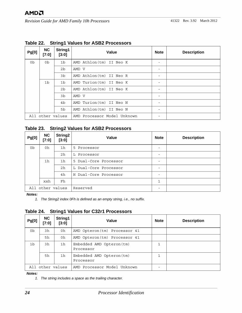
Table 22. String1 Values for ASB2 Processors
Pg[0] NC[7:0]
String1[3:0] Value Note Description
0b 0b 1b AMD Athlon(tm) II Neo K -
2b AMD V -
3b AMD Athlon(tm) II Neo R -
1b 1b AMD Turion(tm) II Neo K -
2b AMD Athlon(tm) II Neo K -
3b AMD V -
4b AMD Turion(tm) II Neo N -
5b AMD Athlon(tm) II Neo N -
All other values AMD Processor Model Unknown -
Table 23. String2 Values for ASB2 Processors
Pg[0] NC[7:0]
String2[3:0] Value Note Description
0b 0h 1h 5 Processor -
2h L Processor -
1h 1h 5 Dual-Core Processor -
2h L Dual-Core Processor -
4h H Dual-Core Processor -
xxh Fh 1
All other values Reserved -
Notes:1. The String2 index 0Fh is defined as an empty string, i.e., no suffix.
Table 24. String1 Values for C32r1 Processors
Pg[0] NC[7:0]
String1[3:0] Value Note Description
0b 3h 0h AMD Opteron(tm) Processor 41
5h 0h AMD Opteron(tm) Processor 41
1b 3h 1h Embedded AMD Opteron(tm) Processor
1
5h 1h Embedded AMD Opteron(tm) Processor
1
All other values AMD Processor Model Unknown -
Notes:1. The string includes a space as the trailing character.
Processor Identification 25
Revision Guide for AMD Family 10h Processors41322 Rev. 3.92 March 2012
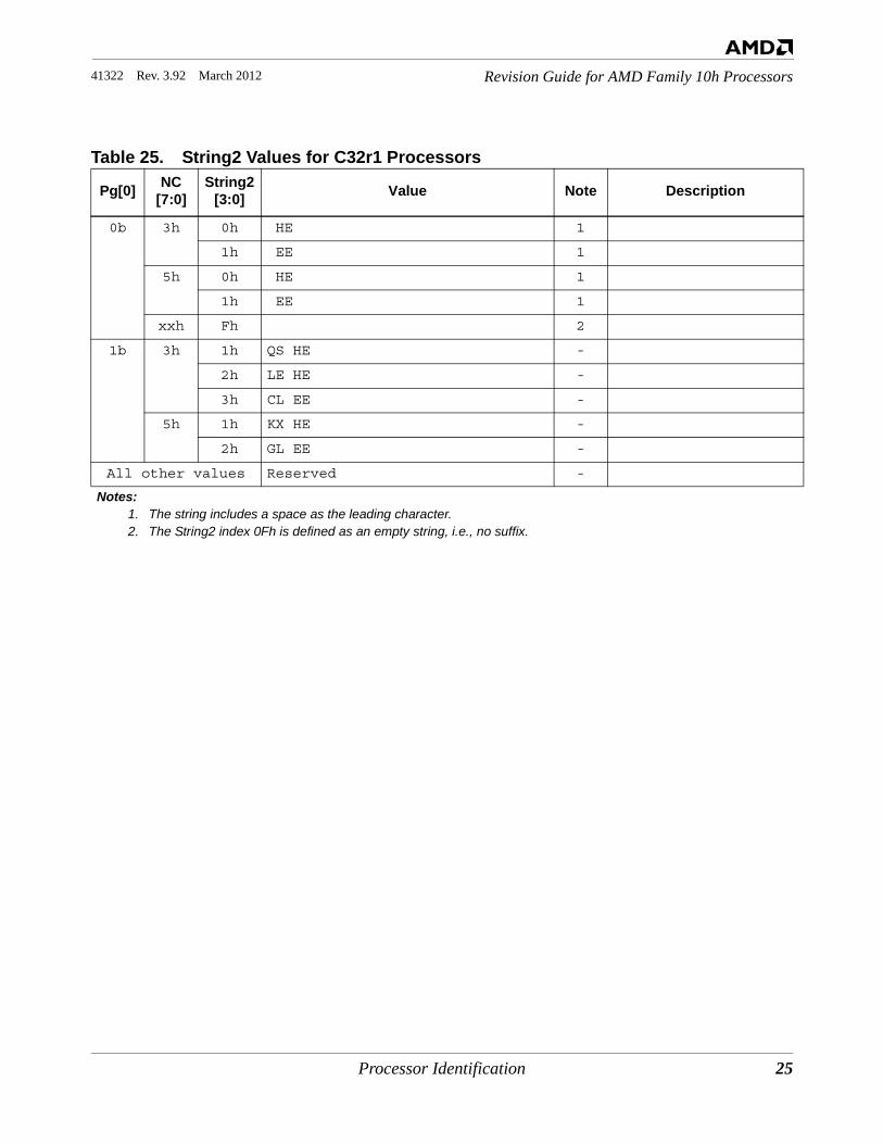
Table 25. String2 Values for C32r1 Processors
Pg[0] NC[7:0]
String2[3:0] Value Note Description
0b 3h 0h HE 1
1h EE 1
5h 0h HE 1
1h EE 1
xxh Fh 2
1b 3h 1h QS HE -
2h LE HE -
3h CL EE -
5h 1h KX HE -
2h GL EE -
All other values Reserved -
Notes:1. The string includes a space as the leading character.2. The String2 index 0Fh is defined as an empty string, i.e., no suffix.
26 F4x164 Fixed Errata Register
41322 Rev. 3.92 March 2012Revision Guide for AMD Family 10h Processors
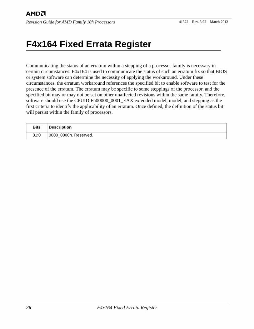
F4x164 Fixed Errata Register
Communicating the status of an erratum within a stepping of a processor family is necessary in certain circumstances. F4x164 is used to communicate the status of such an erratum fix so that BIOS or system software can determine the necessity of applying the workaround. Under these circumstances, the erratum workaround references the specified bit to enable software to test for the presence of the erratum. The erratum may be specific to some steppings of the processor, and the specified bit may or may not be set on other unaffected revisions within the same family. Therefore, software should use the CPUID Fn00000_0001_EAX extended model, model, and stepping as the first criteria to identify the applicability of an erratum. Once defined, the definition of the status bit will persist within the family of processors.
Bits Description
31:0 0000_0000h. Reserved.
MSRC001_0140 OS Visible Work-around MSR0 (OSVW_ID_Length) 27
Revision Guide for AMD Family 10h Processors41322 Rev. 3.92 March 2012
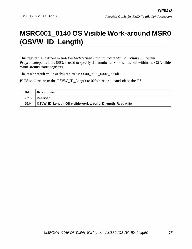
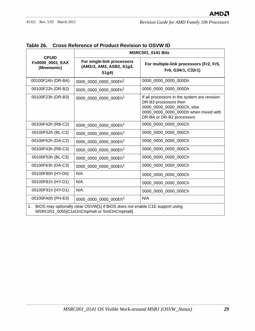
MSRC001_0140 OS Visible Work-around MSR0 (OSVW_ID_Length)
This register, as defined in AMD64 Architecture Programmer’s Manual Volume 2: System Programming, order# 24593, is used to specify the number of valid status bits within the OS Visible Work-around status registers.
The reset default value of this register is 0000_0000_0000_0000h.
BIOS shall program the OSVW_ID_Length to 0004h prior to hand-off to the OS.
Bits Description
63:16 Reserved.
15:0 OSVW_ID_Length: OS visible work-around ID length. Read-write
28 MSRC001_0141 OS Visible Work-around MSR1 (OSVW_Status)
41322 Rev. 3.92 March 2012Revision Guide for AMD Family 10h Processors
MSRC001_0141 OS Visible Work-around MSR1 (OSVW_Status)
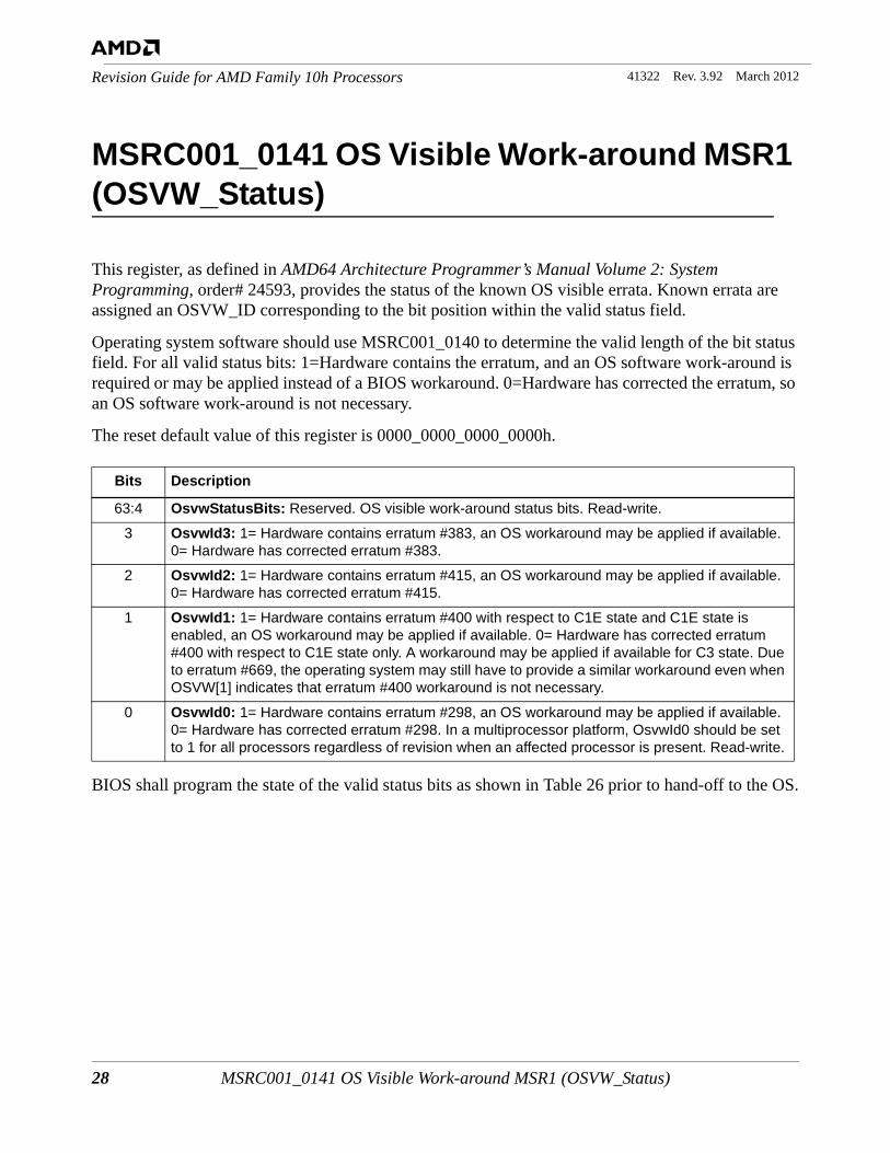
This register, as defined in AMD64 Architecture Programmer’s Manual Volume 2: System Programming, order# 24593, provides the status of the known OS visible errata. Known errata are assigned an OSVW_ID corresponding to the bit position within the valid status field.
Operating system software should use MSRC001_0140 to determine the valid length of the bit status field. For all valid status bits: 1=Hardware contains the erratum, and an OS software work-around is required or may be applied instead of a BIOS workaround. 0=Hardware has corrected the erratum, so an OS software work-around is not necessary.
The reset default value of this register is 0000_0000_0000_0000h.
BIOS shall program the state of the valid status bits as shown in Table 26 prior to hand-off to the OS.
Bits Description
63:4 OsvwStatusBits: Reserved. OS visible work-around status bits. Read-write.
3 OsvwId3: 1= Hardware contains erratum #383, an OS workaround may be applied if available. 0= Hardware has corrected erratum #383.
2 OsvwId2: 1= Hardware contains erratum #415, an OS workaround may be applied if available. 0= Hardware has corrected erratum #415.
1 OsvwId1: 1= Hardware contains erratum #400 with respect to C1E state and C1E state is enabled, an OS workaround may be applied if available. 0= Hardware has corrected erratum #400 with respect to C1E state only. A workaround may be applied if available for C3 state. Due to erratum #669, the operating system may still have to provide a similar workaround even when OSVW[1] indicates that erratum #400 workaround is not necessary.
0 OsvwId0: 1= Hardware contains erratum #298, an OS workaround may be applied if available. 0= Hardware has corrected erratum #298. In a multiprocessor platform, OsvwId0 should be set to 1 for all processors regardless of revision when an affected processor is present. Read-write.
MSRC001_0141 OS Visible Work-around MSR1 (OSVW_Status) 29
Revision Guide for AMD Family 10h Processors41322 Rev. 3.92 March 2012
Table 26. Cross Reference of Product Revision to OSVW ID
CPUID Fn0000_0001_EAX
(Mnemonic)
MSRC001_0141 Bits
For single-link processors (AM2r2, AM3, ASB2, S1g3,
S1g4)
For multiple-link processors (Fr2, Fr5, Fr6, G34r1, C32r1)
00100F2Ah (DR-BA) 0000_0000_0000_000Fh1 0000_0000_0000_000Dh
00100F22h (DR-B2) 0000_0000_0000_000Fh1 0000_0000_0000_000Dh
00100F23h (DR-B3) 0000_0000_0000_000Eh1 If all processors in the system are revision DR-B3 processors then 0000_0000_0000_000Ch, else 0000_0000_0000_000Dh when mixed with DR-BA or DR-B2 processors
00100F42h (RB-C2) 0000_0000_0000_000Eh1 0000_0000_0000_000Ch
00100F52h (BL-C2) 0000_0000_0000_000Eh1 0000_0000_0000_000Ch
00100F62h (DA-C2) 0000_0000_0000_000Eh1 0000_0000_0000_000Ch
00100F43h (RB-C3) 0000_0000_0000_000Eh1 0000_0000_0000_000Ch
00100F53h (BL-C3) 0000_0000_0000_000Eh1 0000_0000_0000_000Ch
00100F63h (DA-C3) 0000_0000_0000_000Eh1 0000_0000_0000_000Ch
00100F80h (HY-D0) N/A 0000_0000_0000_000Ch
00100F81h (HY-D1) N/A 0000_0000_0000_000Ch
00100F91h (HY-D1) N/A 0000_0000_0000_000Ch
00100FA0h (PH-E0) 0000_0000_0000_000Eh1 N/A
1. BIOS may optionally clear OSVW[1] if BIOS does not enable C1E support using MSRC001_0055[C1eOnCmpHalt or SmiOnCmpHalt].
30 Product Errata
41322 Rev. 3.92 March 2012Revision Guide for AMD Family 10h Processors
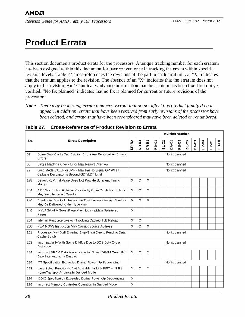
Product Errata
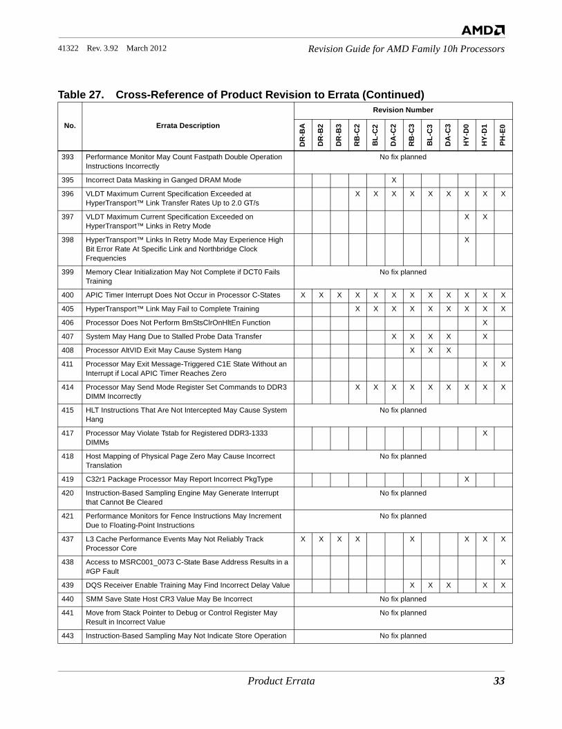
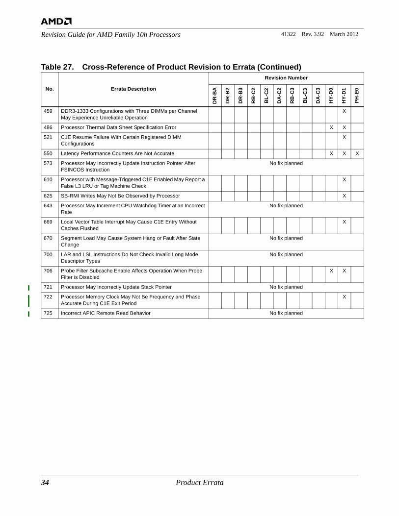
This section documents product errata for the processors. A unique tracking number for each erratum has been assigned within this document for user convenience in tracking the errata within specific revision levels. Table 27 cross-references the revisions of the part to each erratum. An “X” indicates that the erratum applies to the revision. The absence of an “X” indicates that the erratum does not apply to the revision. An “*” indicates advance information that the erratum has been fixed but not yet verified. “No fix planned” indicates that no fix is planned for current or future revisions of the processor.
Note: There may be missing errata numbers. Errata that do not affect this product family do not appear. In addition, errata that have been resolved from early revisions of the processor have been deleted, and errata that have been reconsidered may have been deleted or renumbered.
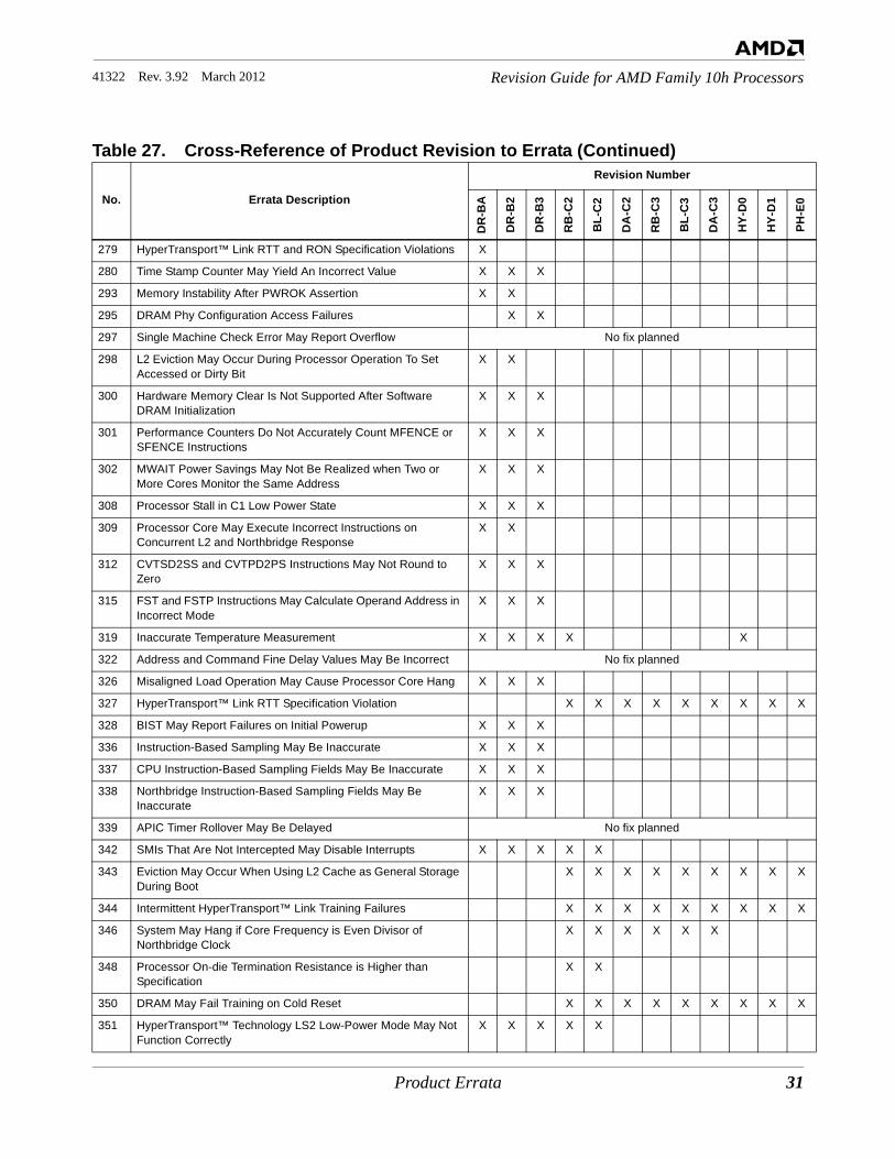
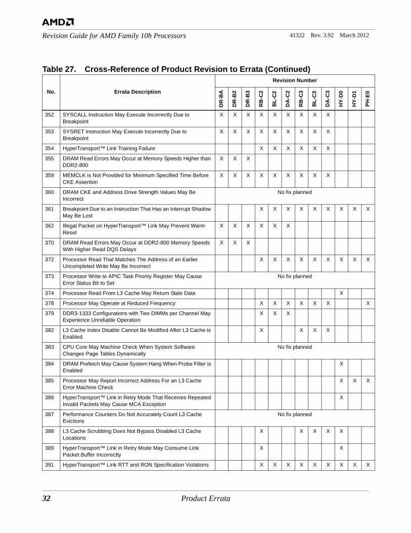
Table 27. Cross-Reference of Product Revision to Errata
No. Errata Description
Revision NumberD
R-B
A
DR
-B2
DR
-B3
RB
-C2
BL-
C2
DA
-C2
RB
-C3
BL-
C3
DA
-C3
HY-
D0
HY-
D1
PH-E
0
57 Some Data Cache Tag Eviction Errors Are Reported As Snoop Errors
No fix planned
60 Single Machine Check Error May Report Overflow No fix planned
77 Long Mode CALLF or JMPF May Fail To Signal GP When Callgate Descriptor is Beyond GDT/LDT Limit
No fix planned
178 Default RdPtrInit Value Does Not Provide Sufficient Timing Margin
X X X
244 A DIV Instruction Followed Closely By Other Divide Instructions May Yield Incorrect Results
X X X
246 Breakpoint Due to An Instruction That Has an Interrupt Shadow May Be Delivered to the Hypervisor
X X X
248 INVLPGA of A Guest Page May Not Invalidate Splintered Pages
X
254 Internal Resource Livelock Involving Cached TLB Reload X X
260 REP MOVS Instruction May Corrupt Source Address X X X
261 Processor May Stall Entering Stop-Grant Due to Pending Data Cache Scrub
No fix planned
263 Incompatibility With Some DIMMs Due to DQS Duty Cycle Distortion
No fix planned
264 Incorrect DRAM Data Masks Asserted When DRAM Controller Data Interleaving Is Enabled
X X X
269 ITT Specification Exceeded During Power-Up Sequencing No fix planned
273 Lane Select Function Is Not Available for Link BIST on 8-Bit HyperTransport™ Links In Ganged Mode
X X X
274 IDDIO Specification Exceeded During Power-Up Sequencing X
278 Incorrect Memory Controller Operation In Ganged Mode X
Product Errata 31
Revision Guide for AMD Family 10h Processors41322 Rev. 3.92 March 2012
279 HyperTransport™ Link RTT and RON Specification Violations X
280 Time Stamp Counter May Yield An Incorrect Value X X X
293 Memory Instability After PWROK Assertion X X
295 DRAM Phy Configuration Access Failures X X
297 Single Machine Check Error May Report Overflow No fix planned
298 L2 Eviction May Occur During Processor Operation To Set Accessed or Dirty Bit
X X
300 Hardware Memory Clear Is Not Supported After Software DRAM Initialization
X X X
301 Performance Counters Do Not Accurately Count MFENCE or SFENCE Instructions
X X X
302 MWAIT Power Savings May Not Be Realized when Two or More Cores Monitor the Same Address
X X X
308 Processor Stall in C1 Low Power State X X X
309 Processor Core May Execute Incorrect Instructions on Concurrent L2 and Northbridge Response
X X
312 CVTSD2SS and CVTPD2PS Instructions May Not Round to Zero
X X X
315 FST and FSTP Instructions May Calculate Operand Address in Incorrect Mode
X X X
319 Inaccurate Temperature Measurement X X X X X
322 Address and Command Fine Delay Values May Be Incorrect No fix planned
326 Misaligned Load Operation May Cause Processor Core Hang X X X
327 HyperTransport™ Link RTT Specification Violation X X X X X X X X X
328 BIST May Report Failures on Initial Powerup X X X
336 Instruction-Based Sampling May Be Inaccurate X X X
337 CPU Instruction-Based Sampling Fields May Be Inaccurate X X X
338 Northbridge Instruction-Based Sampling Fields May Be Inaccurate
X X X
339 APIC Timer Rollover May Be Delayed No fix planned
342 SMIs That Are Not Intercepted May Disable Interrupts X X X X X
343 Eviction May Occur When Using L2 Cache as General Storage During Boot
X X X X X X X X X
344 Intermittent HyperTransport™ Link Training Failures X X X X X X X X X
346 System May Hang if Core Frequency is Even Divisor of Northbridge Clock
X X X X X X
348 Processor On-die Termination Resistance is Higher than Specification
X X
350 DRAM May Fail Training on Cold Reset X X X X X X X X X
351 HyperTransport™ Technology LS2 Low-Power Mode May Not Function Correctly
X X X X X
Table 27. Cross-Reference of Product Revision to Errata (Continued)
No. Errata Description
Revision Number
DR
-BA
DR
-B2
DR
-B3
RB
-C2
BL-
C2
DA
-C2
RB
-C3
BL-
C3
DA
-C3
HY-
D0
HY-
D1
PH-E
0
32 Product Errata
41322 Rev. 3.92 March 2012Revision Guide for AMD Family 10h Processors
352 SYSCALL Instruction May Execute Incorrectly Due to Breakpoint
X X X X X X X X X
353 SYSRET Instruction May Execute Incorrectly Due to Breakpoint
X X X X X X X X X
354 HyperTransport™ Link Training Failure X X X X X X
355 DRAM Read Errors May Occur at Memory Speeds Higher than DDR2-800
X X X
359 MEMCLK is Not Provided for Minimum Specified Time Before CKE Assertion
X X X X X X X X X
360 DRAM CKE and Address Drive Strength Values May Be Incorrect
No fix planned
361 Breakpoint Due to an Instruction That Has an Interrupt Shadow May Be Lost
X X X X X X X X X
362 Illegal Packet on HyperTransport™ Link May Prevent Warm Reset
X X X X X X
370 DRAM Read Errors May Occur at DDR2-800 Memory Speeds With Higher Read DQS Delays
X X X
372 Processor Read That Matches The Address of an Earlier Uncompleted Write May Be Incorrect
X X X X X X X X X
373 Processor Write to APIC Task Priority Register May Cause Error Status Bit to Set
No fix planned
374 Processor Read From L3 Cache May Return Stale Data X
378 Processor May Operate at Reduced Frequency X X X X X X X
379 DDR3-1333 Configurations with Two DIMMs per Channel May Experience Unreliable Operation
X X X
382 L3 Cache Index Disable Cannot Be Modified After L3 Cache is Enabled
X X X X
383 CPU Core May Machine Check When System Software Changes Page Tables Dynamically
No fix planned
384 DRAM Prefetch May Cause System Hang When Probe Filter is Enabled
X
385 Processor May Report Incorrect Address For an L3 Cache Error Machine Check
X X X
386 HyperTransport™ Link in Retry Mode That Receives Repeated Invalid Packets May Cause MCA Exception
X
387 Performance Counters Do Not Accurately Count L3 Cache Evictions
No fix planned
388 L3 Cache Scrubbing Does Not Bypass Disabled L3 Cache Locations
X X X X X
389 HyperTransport™ Link in Retry Mode May Consume Link Packet Buffer Incorrectly
X X
391 HyperTransport™ Link RTT and RON Specification Violations X X X X X X X X X
Table 27. Cross-Reference of Product Revision to Errata (Continued)
No. Errata Description
Revision Number
DR
-BA
DR
-B2
DR
-B3
RB
-C2
BL-
C2
DA
-C2
RB
-C3
BL-
C3
DA
-C3
HY-
D0
HY-
D1
PH-E
0
Product Errata 33
Revision Guide for AMD Family 10h Processors41322 Rev. 3.92 March 2012
393 Performance Monitor May Count Fastpath Double Operation Instructions Incorrectly
No fix planned
395 Incorrect Data Masking in Ganged DRAM Mode X
396 VLDT Maximum Current Specification Exceeded at HyperTransport™ Link Transfer Rates Up to 2.0 GT/s
X X X X X X X X X
397 VLDT Maximum Current Specification Exceeded on HyperTransport™ Links in Retry Mode
X X
398 HyperTransport™ Links In Retry Mode May Experience High Bit Error Rate At Specific Link and Northbridge Clock Frequencies
X
399 Memory Clear Initialization May Not Complete if DCT0 Fails Training
No fix planned
400 APIC Timer Interrupt Does Not Occur in Processor C-States X X X X X X X X X X X X
405 HyperTransport™ Link May Fail to Complete Training X X X X X X X X X
406 Processor Does Not Perform BmStsClrOnHltEn Function X
407 System May Hang Due to Stalled Probe Data Transfer X X X X X
408 Processor AltVID Exit May Cause System Hang X X X
411 Processor May Exit Message-Triggered C1E State Without an Interrupt if Local APIC Timer Reaches Zero
X X
414 Processor May Send Mode Register Set Commands to DDR3 DIMM Incorrectly
X X X X X X X X X
415 HLT Instructions That Are Not Intercepted May Cause System Hang
No fix planned
417 Processor May Violate Tstab for Registered DDR3-1333 DIMMs
X
418 Host Mapping of Physical Page Zero May Cause Incorrect Translation
No fix planned
419 C32r1 Package Processor May Report Incorrect PkgType X
420 Instruction-Based Sampling Engine May Generate Interrupt that Cannot Be Cleared
No fix planned
421 Performance Monitors for Fence Instructions May Increment Due to Floating-Point Instructions
No fix planned
437 L3 Cache Performance Events May Not Reliably Track Processor Core
X X X X X X X X
438 Access to MSRC001_0073 C-State Base Address Results in a #GP Fault
X
439 DQS Receiver Enable Training May Find Incorrect Delay Value X X X X X
440 SMM Save State Host CR3 Value May Be Incorrect No fix planned
441 Move from Stack Pointer to Debug or Control Register May Result in Incorrect Value
No fix planned
443 Instruction-Based Sampling May Not Indicate Store Operation No fix planned
Table 27. Cross-Reference of Product Revision to Errata (Continued)
No. Errata Description
Revision Number
DR
-BA
DR
-B2
DR
-B3
RB
-C2
BL-
C2
DA
-C2
RB
-C3
BL-
C3
DA
-C3
HY-
D0
HY-
D1
PH-E
0
34 Product Errata
41322 Rev. 3.92 March 2012Revision Guide for AMD Family 10h Processors
459 DDR3-1333 Configurations with Three DIMMs per Channel May Experience Unreliable Operation
X
486 Processor Thermal Data Sheet Specification Error X X
521 C1E Resume Failure With Certain Registered DIMM Configurations
X
550 Latency Performance Counters Are Not Accurate X X X
573 Processor May Incorrectly Update Instruction Pointer After FSINCOS Instruction
No fix planned
610 Processor with Message-Triggered C1E Enabled May Report a False L3 LRU or Tag Machine Check
X
625 SB-RMI Writes May Not Be Observed by Processor X
643 Processor May Increment CPU Watchdog Timer at an Incorrect Rate
No fix planned
669 Local Vector Table Interrupt May Cause C1E Entry Without Caches Flushed
X
670 Segment Load May Cause System Hang or Fault After State Change
No fix planned
700 LAR and LSL Instructions Do Not Check Invalid Long Mode Descriptor Types
No fix planned
706 Probe Filter Subcache Enable Affects Operation When Probe Filter is Disabled
X X
721 Processor May Incorrectly Update Stack Pointer No fix planned
722 Processor Memory Clock May Not Be Frequency and Phase Accurate During C1E Exit Period
X
725 Incorrect APIC Remote Read Behavior No fix planned
Table 27. Cross-Reference of Product Revision to Errata (Continued)
No. Errata Description
Revision Number
DR
-BA
DR
-B2
DR
-B3
RB
-C2
BL-
C2
DA
-C2
RB
-C3
BL-
C3
DA
-C3
HY-
D0
HY-
D1
PH-E
0
Product Errata 35
Revision Guide for AMD Family 10h Processors41322 Rev. 3.92 March 2012
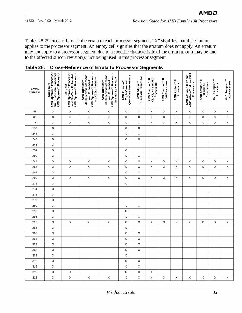
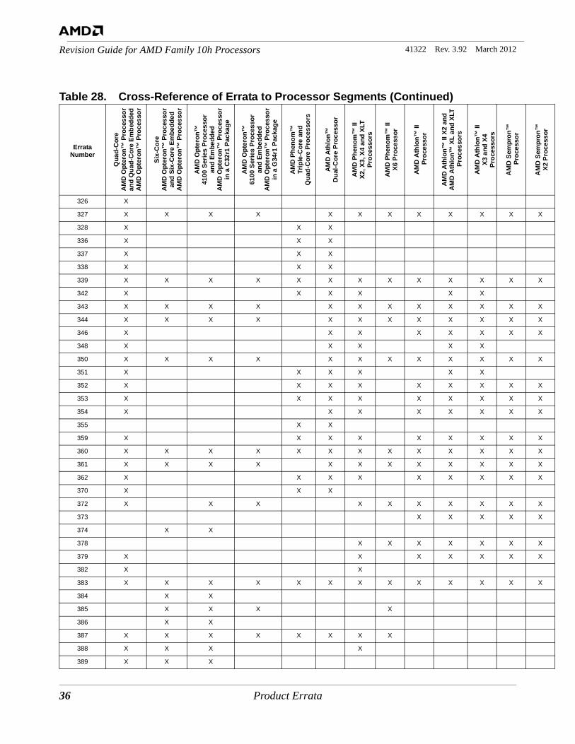
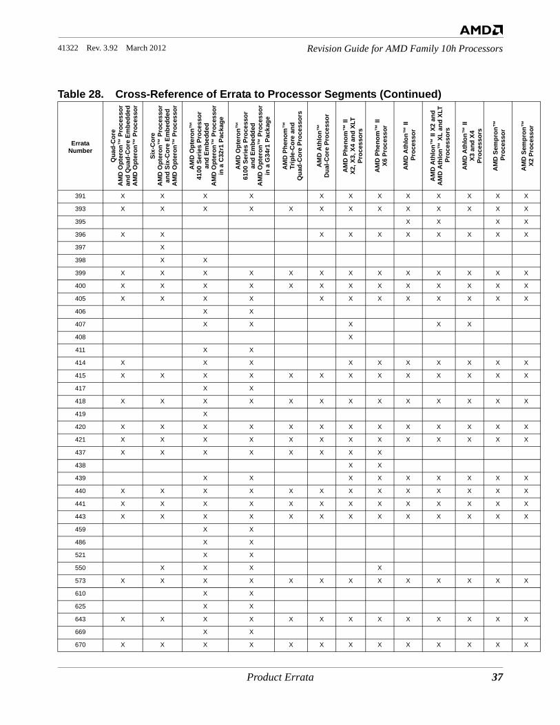
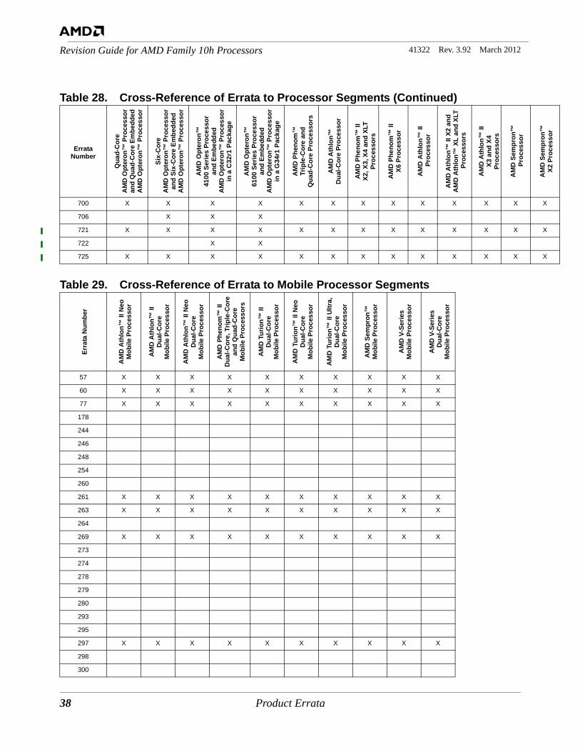
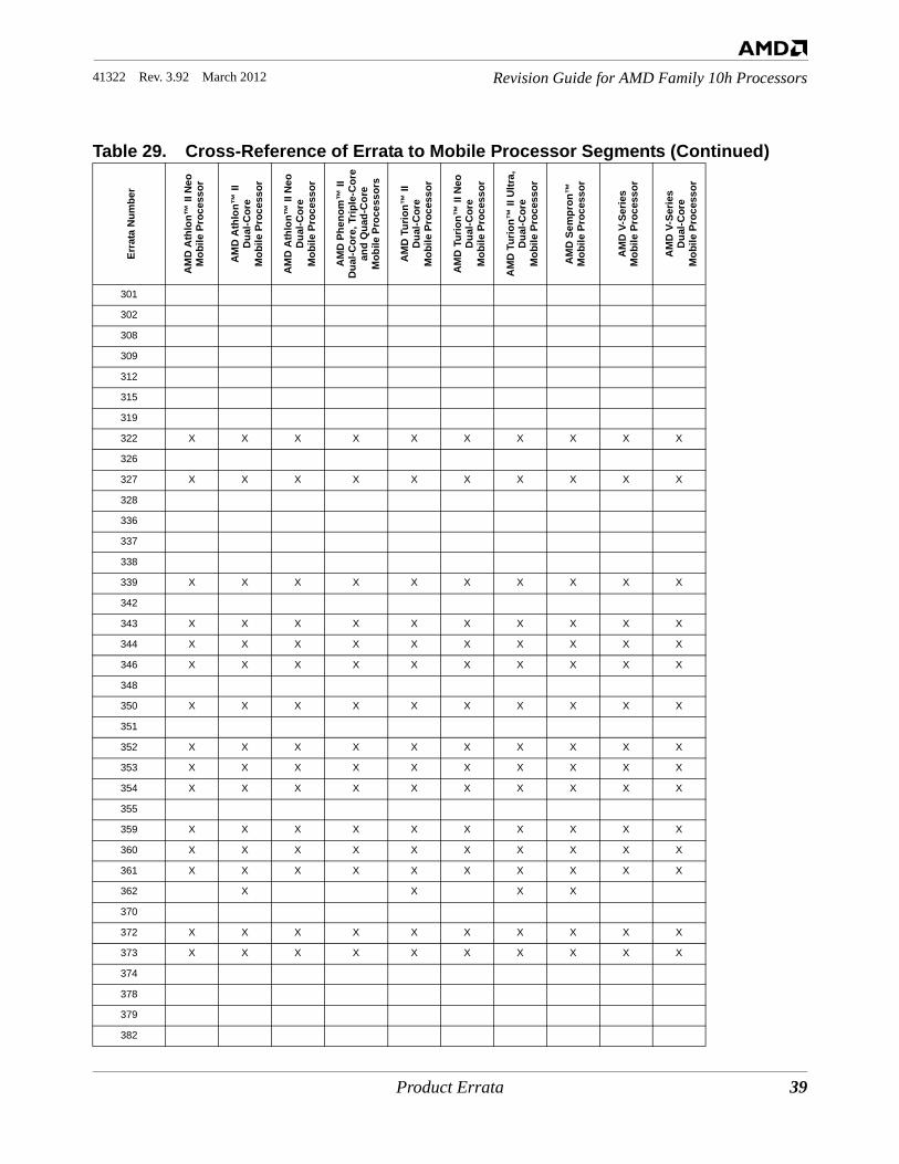
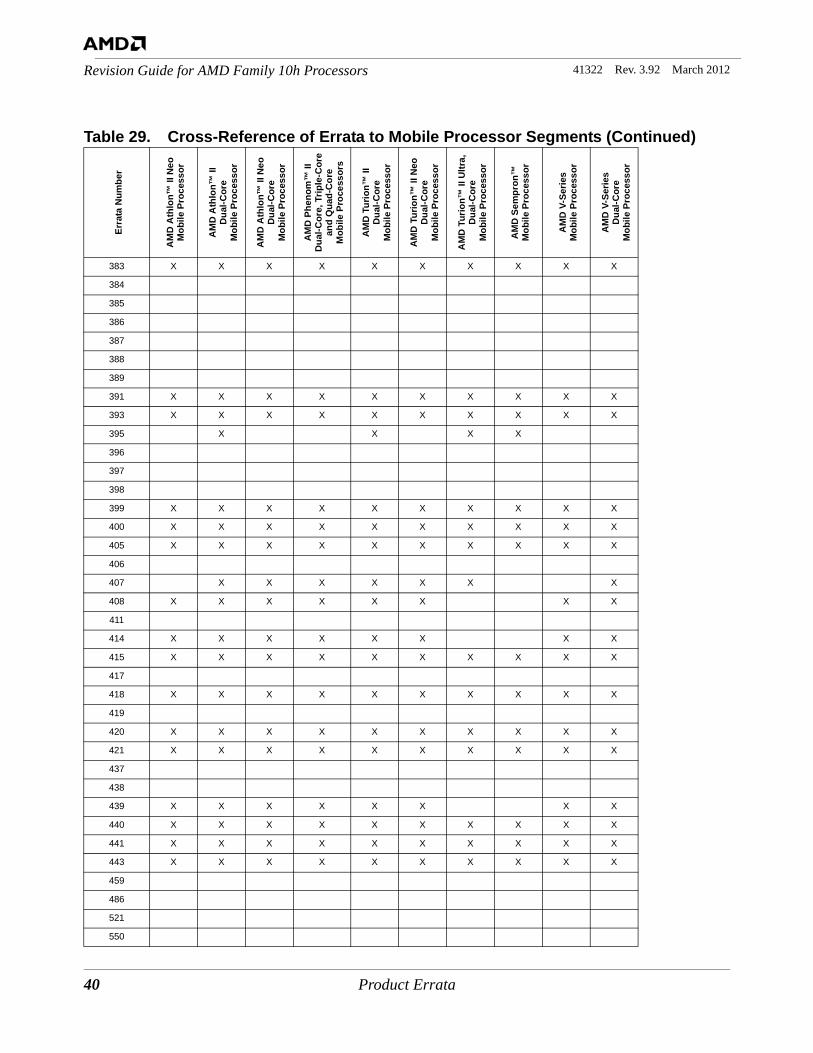
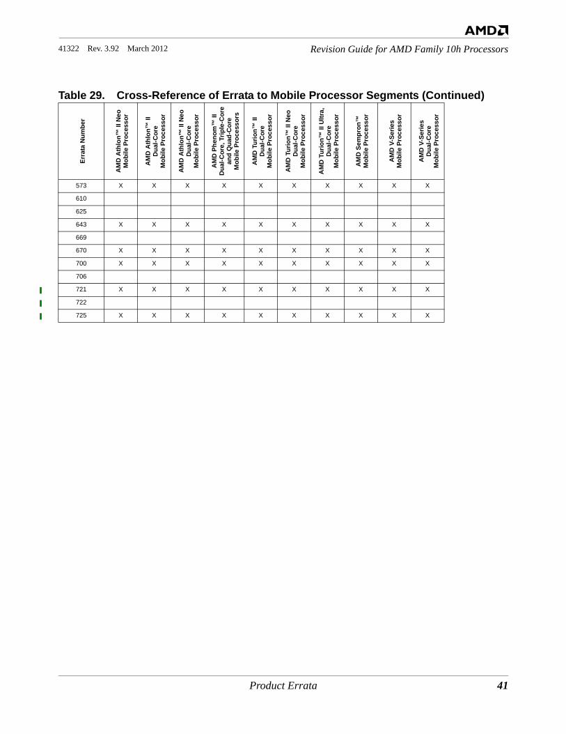
Tables 28-29 cross-reference the errata to each processor segment. “X” signifies that the erratum applies to the processor segment. An empty cell signifies that the erratum does not apply. An erratum may not apply to a processor segment due to a specific characteristic of the erratum, or it may be due to the affected silicon revision(s) not being used in this processor segment.
Table 28. Cross-Reference of Errata to Processor Segments
Errata Number
Qua
d-C
ore
AM
DO
pter
on™
Pro
cess
oran
d Q
uad-
Cor
e Em
bedd
edA
MD
Opt
eron
™ P
roce
ssor
Six-
Cor
eA
MD
Opt
eron
™ P
roce
ssor
and
Six-
Cor
e Em
bedd
edA
MD
Opt
eron
™ P
roce
ssor
AM
DO
pter
on™
4100
Ser
ies
Proc
esso
ran
d Em
bedd
edA
MD
Opt
eron
™ P
roce
ssor
in a
C32
r1 P
acka
ge
AM
DO
pter
on™
6100
Ser
ies
Proc
esso
ran
d Em
bedd
edA
MD
Opt
eron
™ P
roce
ssor
in a
G34
r1 P
acka
ge
AM
DPh
enom
™Tr
iple
-Cor
e an
dQ
uad-
Cor
e Pr
oces
sors
AM
DA
thlo
n™D
ual-C
ore
Proc
esso
r
AM
DPh
enom
™ II
X2, X
3, X
4 an
d XL
TPr
oces
sors
AM
DPh
enom
™ II
X6 P
roce
ssor
AM
DA
thlo
n™ II
Pro
cess
or
AM
DA
thlo
n™ II
X2
and
AM
DA
thlo
n™ X
L an
d XL
T P
roce
ssor
s
AM
DA
thlo
n™ II
X3 a
nd X
4Pr
oces
sors
AM
DSe
mpr
on™
Pro
cess
or
AM
DSe
mpr
on™
X2 P
roce
ssor
57 X X X X X X X X X X X X X
60 X X X X X X X X X X X X X
77 X X X X X X X X X X X X X
178 X X X
244 X X X
246 X X X
248 X
254 X X
260 X X X
261 X X X X X X X X X X X X X
263 X X X X X X X X X X X X X
264 X X X
269 X X X X X X X X X X X X X
273 X X X
274 X
278 X
279 X
280 X X X
293 X X
295 X X X
297 X X X X X X X X X X X X X
298 X X
300 X X X
301 X X X
302 X X X
308 X X X
309 X X
312 X X X
315 X X X
319 X X X X X
322 X X X X X X X X X X X X X
36 Product Errata
41322 Rev. 3.92 March 2012Revision Guide for AMD Family 10h Processors
326 X
327 X X X X X X X X X X X X
328 X X X
336 X X X
337 X X X
338 X X X
339 X X X X X X X X X X X X X
342 X X X X X X
343 X X X X X X X X X X X X
344 X X X X X X X X X X X X
346 X X X X X X X X
348 X X X X X
350 X X X X X X X X X X X X
351 X X X X X X
352 X X X X X X X X X
353 X X X X X X X X X
354 X X X X X X X X
355 X X
359 X X X X X X X X X
360 X X X X X X X X X X X X X
361 X X X X X X X X X X X X
362 X X X X X X X X X
370 X X X
372 X X X X X X X X X X
373 X X X X X
374 X X
378 X X X X X X X
379 X X X X X X X
382 X X
383 X X X X X X X X X X X X X
384 X X
385 X X X X
386 X X
387 X X X X X X X X
388 X X X X
389 X X X
Table 28. Cross-Reference of Errata to Processor Segments (Continued)
Errata Number
Qua
d-C
ore
AM
DO
pter
on™
Pro
cess
oran
d Q
uad-
Cor
e Em
bedd
edA
MD
Opt
eron
™ P
roce
ssor
Six-
Cor
eA
MD
Opt
eron
™ P
roce
ssor
and
Six-
Cor
e Em
bedd
edA
MD
Opt
eron
™ P
roce
ssor
AM
DO
pter
on™
4100
Ser
ies
Proc
esso
ran
d Em
bedd
edA
MD
Opt
eron
™ P
roce
ssor
in a
C32
r1 P
acka
ge
AM
DO
pter
on™
6100
Ser
ies
Proc
esso
ran
d Em
bedd
edA
MD
Opt
eron
™ P
roce
ssor
in a
G34
r1 P
acka
ge
AM
DPh
enom
™Tr
iple
-Cor
e an
dQ
uad-
Cor
e Pr
oces
sors
AM
DA
thlo
n™D
ual-C
ore
Proc
esso
r
AM
DPh
enom
™ II
X2, X
3, X
4 an
d XL
TPr
oces
sors
AM
DPh
enom
™ II
X6 P
roce
ssor
AM
DA
thlo
n™ II
Pro
cess
or
AM
DA
thlo
n™ II
X2
and
AM
DA
thlo
n™ X
L an
d XL
T P
roce
ssor
s
AM
DA
thlo
n™ II
X3 a
nd X
4Pr
oces
sors
AM
DSe
mpr
on™
Pro
cess
or
AM
DSe
mpr
on™
X2 P
roce
ssor
Product Errata 37
Revision Guide for AMD Family 10h Processors41322 Rev. 3.92 March 2012
391 X X X X X X X X X X X X
393 X X X X X X X X X X X X X
395 X X X X
396 X X X X X X X X X X
397 X
398 X X
399 X X X X X X X X X X X X X
400 X X X X X X X X X X X X X
405 X X X X X X X X X X X X
406 X X
407 X X X X X
408 X
411 X X
414 X X X X X X X X X X
415 X X X X X X X X X X X X X
417 X X
418 X X X X X X X X X X X X X
419 X
420 X X X X X X X X X X X X X
421 X X X X X X X X X X X X X
437 X X X X X X X X
438 X X
439 X X X X X X X X X
440 X X X X X X X X X X X X X
441 X X X X X X X X X X X X X
443 X X X X X X X X X X X X X
459 X X
486 X X
521 X X
550 X X X X
573 X X X X X X X X X X X X X
610 X X
625 X X
643 X X X X X X X X X X X X X
669 X X
670 X X X X X X X X X X X X X
Table 28. Cross-Reference of Errata to Processor Segments (Continued)
Errata Number
Qua
d-C
ore
AM
DO
pter
on™
Pro
cess
oran
d Q
uad-
Cor
e Em
bedd
edA
MD
Opt
eron
™ P
roce
ssor
Six-
Cor
eA
MD
Opt
eron
™ P
roce
ssor
and
Six-
Cor
e Em
bedd
edA
MD
Opt
eron
™ P
roce
ssor
AM
DO
pter
on™
4100
Ser
ies
Proc
esso
ran
d Em
bedd
edA
MD
Opt
eron
™ P
roce
ssor
in a
C32
r1 P
acka
ge
AM
DO
pter
on™
6100
Ser
ies
Proc
esso
ran
d Em
bedd
edA
MD
Opt
eron
™ P
roce
ssor
in a
G34
r1 P
acka
ge
AM
DPh
enom
™Tr
iple
-Cor
e an
dQ
uad-
Cor
e Pr
oces
sors
AM
DA
thlo
n™D
ual-C
ore
Proc
esso
r
AM
DPh
enom
™ II
X2, X
3, X
4 an
d XL
TPr
oces
sors
AM
DPh
enom
™ II
X6 P
roce
ssor
AM
DA
thlo
n™ II
Pro
cess
or
AM
DA
thlo
n™ II
X2
and
AM
DA
thlo
n™ X
L an
d XL
T P
roce
ssor
s
AM
DA
thlo
n™ II
X3 a
nd X
4Pr
oces
sors
AM
DSe
mpr
on™
Pro
cess
or
AM
DSe
mpr
on™
X2 P
roce
ssor
38 Product Errata
41322 Rev. 3.92 March 2012Revision Guide for AMD Family 10h Processors
700 X X X X X X X X X X X X X
706 X X X
721 X X X X X X X X X X X X X
722 X X
725 X X X X X X X X X X X X X
Table 29. Cross-Reference of Errata to Mobile Processor Segments
Erra
ta N
umbe
r
AM
DA
thlo
n™ II
Neo
Mob
ile P
roce
ssor
AM
DA
thlo
n™ II
Dua
l-Cor
eM
obile
Pro
cess
or
AM
DA
thlo
n™ II
Neo
Dua
l-Cor
eM
obile
Pro
cess
or
AM
DPh
enom
™ II
Dua
l-Cor
e, T
riple
-Cor
ean
d Q
uad-
Cor
eM
obile
Pro
cess
ors
AM
DTu
rion™
IID
ual-C
ore
Mob
ile P
roce
ssor
AM
DTu
rion™
II N
eoD
ual-C
ore
Mob
ile P
roce
ssor
AM
DTu
rion™
II U
ltra,
Dua
l-Cor
eM
obile
Pro
cess
or
AM
DSe
mpr
on™
Mob
ile P
roce
ssor
AM
D V
-Ser
ies
Mob
ile P
roce
ssor
AM
D V
-Ser
ies
Dua
l-Cor
eM
obile
Pro
cess
or
57 X X X X X X X X X X
60 X X X X X X X X X X
77 X X X X X X X X X X
178
244
246
248
254
260
261 X X X X X X X X X X
263 X X X X X X X X X X
264
269 X X X X X X X X X X
273
274
278
279
280
293
295
297 X X X X X X X X X X
298
300
Table 28. Cross-Reference of Errata to Processor Segments (Continued)
Errata Number
Qua
d-C
ore
AM
DO
pter
on™
Pro
cess
oran
d Q
uad-
Cor
e Em
bedd
edA
MD
Opt
eron
™ P
roce
ssor
Six-
Cor
eA
MD
Opt
eron
™ P
roce
ssor
and
Six-
Cor
e Em
bedd
edA
MD
Opt
eron
™ P
roce
ssor
AM
DO
pter
on™
4100
Ser
ies
Proc
esso
ran
d Em
bedd
edA
MD
Opt
eron
™ P
roce
ssor
in a
C32
r1 P
acka
ge
AM
DO
pter
on™
6100
Ser
ies
Proc
esso
ran
d Em
bedd
edA
MD
Opt
eron
™ P
roce
ssor
in a
G34
r1 P
acka
ge
AM
DPh
enom
™Tr
iple
-Cor
e an
dQ
uad-
Cor
e Pr
oces
sors
AM
DA
thlo
n™D
ual-C
ore
Proc
esso
r
AM
DPh
enom
™ II
X2, X
3, X
4 an
d XL
TPr
oces
sors
AM
DPh
enom
™ II
X6 P
roce
ssor
AM
DA
thlo
n™ II
Pro
cess
or
AM
DA
thlo
n™ II
X2
and
AM
DA
thlo
n™ X
L an
d XL
T P
roce
ssor
s
AM
DA
thlo
n™ II
X3 a
nd X
4Pr
oces
sors
AM
DSe
mpr
on™
Pro
cess
or
AM
DSe
mpr
on™
X2 P
roce
ssor
Product Errata 39
Revision Guide for AMD Family 10h Processors41322 Rev. 3.92 March 2012
301
302
308
309
312
315
319
322 X X X X X X X X X X
326
327 X X X X X X X X X X
328
336
337
338
339 X X X X X X X X X X
342
343 X X X X X X X X X X
344 X X X X X X X X X X
346 X X X X X X X X X X
348
350 X X X X X X X X X X
351
352 X X X X X X X X X X
353 X X X X X X X X X X
354 X X X X X X X X X X
355
359 X X X X X X X X X X
360 X X X X X X X X X X
361 X X X X X X X X X X
362 X X X X
370
372 X X X X X X X X X X
373 X X X X X X X X X X
374
378
379
382
Table 29. Cross-Reference of Errata to Mobile Processor Segments (Continued)Er
rata
Num
ber
AM
DA
thlo
n™ II
Neo
Mob
ile P
roce
ssor
AM
DA
thlo
n™ II
Dua
l-Cor
eM
obile
Pro
cess
or
AM
DA
thlo
n™ II
Neo
Dua
l-Cor
eM
obile
Pro
cess
or
AM
DPh
enom
™ II
Dua
l-Cor
e, T
riple
-Cor
ean
d Q
uad-
Cor
eM
obile
Pro
cess
ors
AM
DTu
rion™
IID
ual-C
ore
Mob
ile P
roce
ssor
AM
DTu
rion™
II N
eoD
ual-C
ore
Mob
ile P
roce
ssor
AM
DTu
rion™
II U
ltra,
Dua
l-Cor
eM
obile
Pro
cess
or
AM
DSe
mpr
on™
Mob
ile P
roce
ssor
AM
D V
-Ser
ies
Mob
ile P
roce
ssor
AM
D V
-Ser
ies
Dua
l-Cor
eM
obile
Pro
cess
or
40 Product Errata
41322 Rev. 3.92 March 2012Revision Guide for AMD Family 10h Processors
383 X X X X X X X X X X
384
385
386
387
388
389
391 X X X X X X X X X X
393 X X X X X X X X X X
395 X X X X
396
397
398
399 X X X X X X X X X X
400 X X X X X X X X X X
405 X X X X X X X X X X
406
407 X X X X X X X
408 X X X X X X X X
411
414 X X X X X X X X
415 X X X X X X X X X X
417
418 X X X X X X X X X X
419
420 X X X X X X X X X X
421 X X X X X X X X X X
437
438
439 X X X X X X X X
440 X X X X X X X X X X
441 X X X X X X X X X X
443 X X X X X X X X X X
459
486
521
550
Table 29. Cross-Reference of Errata to Mobile Processor Segments (Continued)Er
rata
Num
ber
AM
DA
thlo
n™ II
Neo
Mob
ile P
roce
ssor
AM
DA
thlo
n™ II
Dua
l-Cor
eM
obile
Pro
cess
or
AM
DA
thlo
n™ II
Neo
Dua
l-Cor
eM
obile
Pro
cess
or
AM
DPh
enom
™ II
Dua
l-Cor
e, T
riple
-Cor
ean
d Q
uad-
Cor
eM
obile
Pro
cess
ors
AM
DTu
rion™
IID
ual-C
ore
Mob
ile P
roce
ssor
AM
DTu
rion™
II N
eoD
ual-C
ore
Mob
ile P
roce
ssor
AM
DTu
rion™
II U
ltra,
Dua
l-Cor
eM
obile
Pro
cess
or
AM
DSe
mpr
on™
Mob
ile P
roce
ssor
AM
D V
-Ser
ies
Mob
ile P
roce
ssor
AM
D V
-Ser
ies
Dua
l-Cor
eM
obile
Pro
cess
or
Product Errata 41
Revision Guide for AMD Family 10h Processors41322 Rev. 3.92 March 2012
573 X X X X X X X X X X
610
625
643 X X X X X X X X X X
669
670 X X X X X X X X X X
700 X X X X X X X X X X
706
721 X X X X X X X X X X
722
725 X X X X X X X X X X
Table 29. Cross-Reference of Errata to Mobile Processor Segments (Continued)Er
rata
Num
ber
AM
DA
thlo
n™ II
Neo
Mob
ile P
roce
ssor
AM
DA
thlo
n™ II
Dua
l-Cor
eM
obile
Pro
cess
or
AM
DA
thlo
n™ II
Neo
Dua
l-Cor
eM
obile
Pro
cess
or
AM
DPh
enom
™ II
Dua
l-Cor
e, T
riple
-Cor
ean
d Q
uad-
Cor
eM
obile
Pro
cess
ors
AM
DTu
rion™
IID
ual-C
ore
Mob
ile P
roce
ssor
AM
DTu
rion™
II N
eoD
ual-C
ore
Mob
ile P
roce
ssor
AM
DTu
rion™
II U
ltra,
Dua
l-Cor
eM
obile
Pro
cess
or
AM
DSe
mpr
on™
Mob
ile P
roce
ssor
AM
D V
-Ser
ies
Mob
ile P
roce
ssor
AM
D V
-Ser
ies
Dua
l-Cor
eM
obile
Pro
cess
or
42 Product Errata
41322 Rev. 3.92 March 2012Revision Guide for AMD Family 10h Processors
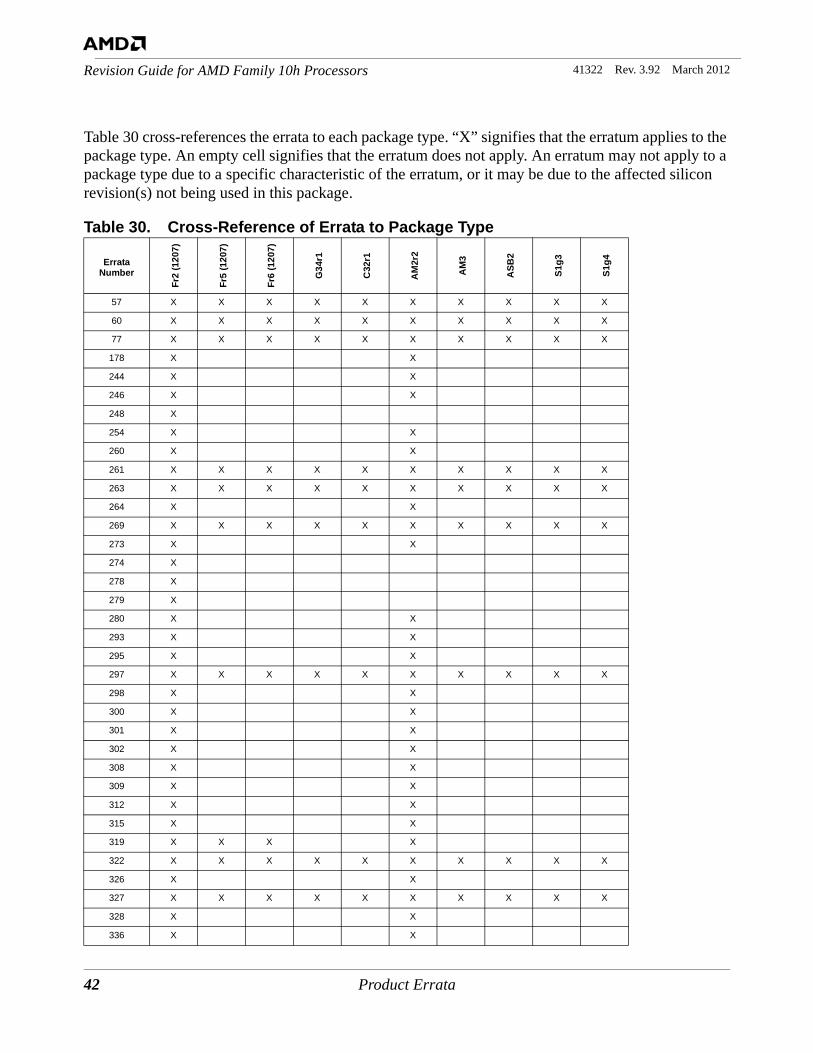
Table 30 cross-references the errata to each package type. “X” signifies that the erratum applies to the package type. An empty cell signifies that the erratum does not apply. An erratum may not apply to a package type due to a specific characteristic of the erratum, or it may be due to the affected silicon revision(s) not being used in this package.
Table 30. Cross-Reference of Errata to Package Type
Errata Number
Fr2
(120
7)
Fr5
(120
7)
Fr6
(120
7)
G34
r1
C32
r1
AM
2r2
AM
3
ASB
2
S1g3
S1g4
57 X X X X X X X X X X
60 X X X X X X X X X X
77 X X X X X X X X X X
178 X X
244 X X
246 X X
248 X
254 X X
260 X X
261 X X X X X X X X X X
263 X X X X X X X X X X
264 X X
269 X X X X X X X X X X
273 X X
274 X
278 X
279 X
280 X X
293 X X
295 X X
297 X X X X X X X X X X
298 X X
300 X X
301 X X
302 X X
308 X X
309 X X
312 X X
315 X X
319 X X X X
322 X X X X X X X X X X
326 X X
327 X X X X X X X X X X
328 X X
336 X X
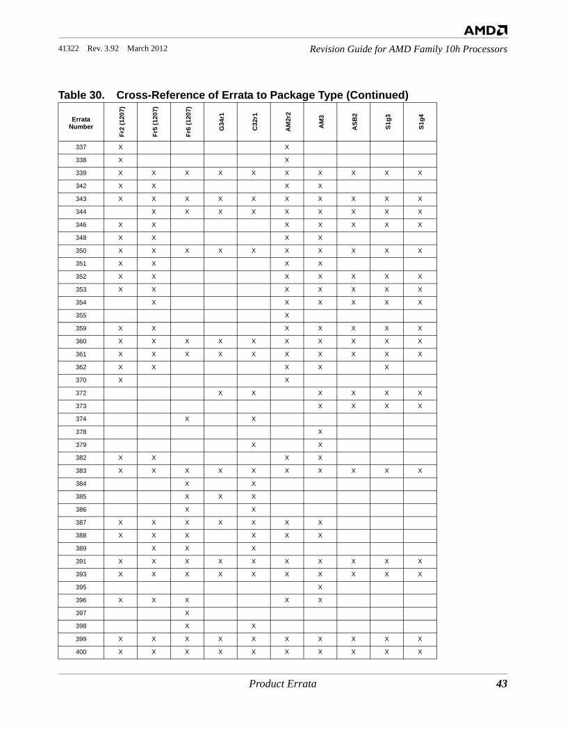
Product Errata 43
Revision Guide for AMD Family 10h Processors41322 Rev. 3.92 March 2012
337 X X
338 X X
339 X X X X X X X X X X
342 X X X X
343 X X X X X X X X X X
344 X X X X X X X X X
346 X X X X X X X
348 X X X X
350 X X X X X X X X X X
351 X X X X
352 X X X X X X X
353 X X X X X X X
354 X X X X X X
355 X
359 X X X X X X X
360 X X X X X X X X X X
361 X X X X X X X X X X
362 X X X X X
370 X X
372 X X X X X X
373 X X X X
374 X X
378 X
379 X X
382 X X X X
383 X X X X X X X X X X
384 X X
385 X X X
386 X X
387 X X X X X X X
388 X X X X X X
389 X X X
391 X X X X X X X X X X
393 X X X X X X X X X X
395 X
396 X X X X X
397 X
398 X X
399 X X X X X X X X X X
400 X X X X X X X X X X
Table 30. Cross-Reference of Errata to Package Type (Continued)
Errata Number
Fr2
(120
7)
Fr5
(120
7)
Fr6
(120
7)
G34
r1
C32
r1
AM
2r2
AM
3
ASB
2
S1g3
S1g4
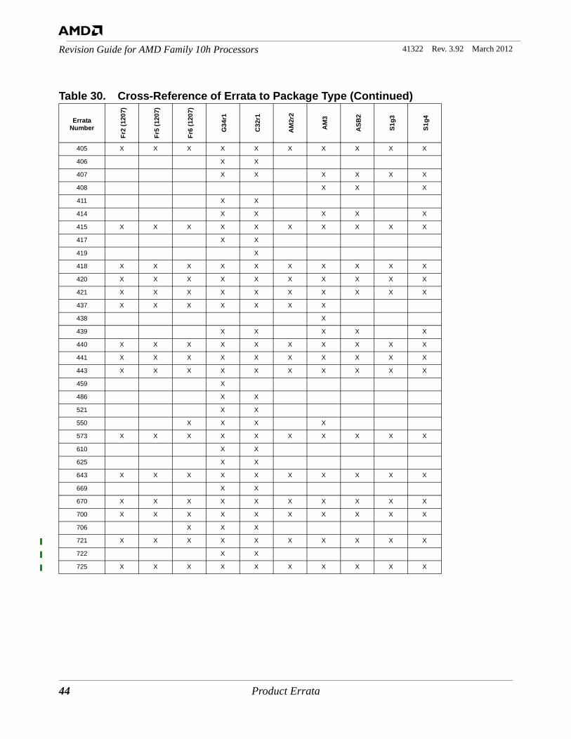
44 Product Errata
41322 Rev. 3.92 March 2012Revision Guide for AMD Family 10h Processors
405 X X X X X X X X X X
406 X X
407 X X X X X X
408 X X X
411 X X
414 X X X X X
415 X X X X X X X X X X
417 X X
419 X
418 X X X X X X X X X X
420 X X X X X X X X X X
421 X X X X X X X X X X
437 X X X X X X X
438 X
439 X X X X X
440 X X X X X X X X X X
441 X X X X X X X X X X
443 X X X X X X X X X X
459 X
486 X X
521 X X
550 X X X X
573 X X X X X X X X X X
610 X X
625 X X
643 X X X X X X X X X X
669 X X
670 X X X X X X X X X X
700 X X X X X X X X X X
706 X X X
721 X X X X X X X X X X
722 X X
725 X X X X X X X X X X
Table 30. Cross-Reference of Errata to Package Type (Continued)
Errata Number
Fr2
(120
7)
Fr5
(120
7)
Fr6
(120
7)
G34
r1
C32
r1
AM
2r2
AM
3
ASB
2
S1g3
S1g4
Product Errata 45
Revision Guide for AMD Family 10h Processors41322 Rev. 3.92 March 2012
57 Some Data Cache Tag Eviction Errors Are Reported As Snoop Errors
DescriptionIn some cases, the machine check error code on a data cache (DC) tag array parity error erroneously classifies an eviction error as a snoop error.
The common cases of cache line replacements and external probes are classified correctly (as eviction and snoop respectively). The erroneous cases occur when a tag error is detected during a DC eviction that was generated by a hardware prefetch, a cache line state change operation, or a number of other internal microarchitectural events. In such cases, the error code logged in the DC Machine Check Status register (MC0_STATUS, MSR0000_0401) erroneously indicates a snoop error.
Potential Effect on SystemInternally detected DC tag errors may be reported to software as having been detected by snoops. Depending upon machine check software architecture, the system response to such errors may be broader than necessary.
Suggested WorkaroundNone required.
Fix PlannedNo
46 Product Errata
41322 Rev. 3.92 March 2012Revision Guide for AMD Family 10h Processors
60 Single Machine Check Error May Report OverflowDescriptionA single parity error encountered in the data cache tag array may incorrectly report the detection of multiple errors, as indicated by the overflow bit of the DC Machine Check Status register (bit 62 of MSR0000_0401).
Potential Effect on SystemSystem software may be informed of a machine check overflow when only a single error was actually encountered.
Suggested WorkaroundDo not rely on the state of the OVER bit in the DC Machine Check Status register.
Fix PlannedNo
Product Errata 47
Revision Guide for AMD Family 10h Processors41322 Rev. 3.92 March 2012
77 Long Mode CALLF or JMPF May Fail To Signal GP When Callgate Descriptor is Beyond GDT/LDT Limit
DescriptionIf the target selector of a far call or far jump (CALLF or JMPF) instruction references a 16-byte long mode system descriptor where any of the last 8 bytes are beyond the GDT or LDT limit, the processor fails to report a General Protection fault.
Potential Effect on SystemNone expected, since the operating system typically aligns the GDT/LDT limit such that all descriptors are legal. However, in the case of erroneous operating system software, the above described GP fault will not be signaled, resulting in unpredictable system failure.
Suggested WorkaroundNone required, it is anticipated that long mode operating system software will ensure the GDT and LDT limits are set high enough to cover the larger (16-byte) long mode system descriptors.
Fix PlannedNo
48 Product Errata
41322 Rev. 3.92 March 2012Revision Guide for AMD Family 10h Processors
178 Default RdPtrInit Value Does Not Provide Sufficient Timing Margin
DescriptionInsufficient separation of the read pointer and write pointer in the synchronization FIFO can lead to setup violations in the transmit FIFO.
Potential Effect on SystemThe setup violations may lead to data corruption.
Suggested WorkaroundBIOS should program F2x[1, 0]78[3:0] (RdPtrInit) to 5h.
Fix PlannedYes
Product Errata 49
Revision Guide for AMD Family 10h Processors41322 Rev. 3.92 March 2012
244 A DIV Instruction Followed Closely By Other Divide Instructions May Yield Incorrect Results
DescriptionA DIV instruction with a dividend less than 64 that is followed in close proximity by a DIV, IDIV, or AAM instruction may produce incorrect results.
Potential Effect on SystemPossible data corruption.
Suggested WorkaroundContact your AMD representative for information on a BIOS update.
Fix PlannedYes
50 Product Errata
41322 Rev. 3.92 March 2012Revision Guide for AMD Family 10h Processors
246 Breakpoint Due to An Instruction That Has an Interrupt Shadow May Be Delivered to the Hypervisor
DescriptionA #DB exception occurring in guest mode may be delivered in the host context under the following conditions:
• A trap-type #DB exception is generated in guest mode during execution of an instruction with an interrupt shadow, and
• The instruction that generated the exception is immediately followed by an instruction resulting in #VMEXIT.
Potential Effect on SystemUnpredictable results due to an unexpected #DB exception.
Suggested WorkaroundThe hypervisor should have a valid interrupt gate in the IDT of the #DB handler entry and the handler must be able to determine that this event has occurred. If the event is detected, the handler should execute an IRET back to the hypervisor; one method that could be used to evaluate for this condition is to compare the RIP pushed on the stack to the RIP of the instruction following VMRUN, if they are equivalent then this event has occurred.
Fix PlannedYes
Product Errata 51
Revision Guide for AMD Family 10h Processors41322 Rev. 3.92 March 2012
248 INVLPGA of A Guest Page May Not Invalidate Splintered PagesDescriptionWhen an address mapped by a guest uses a larger page size than the host, the TLB entry created uses the size of the smaller page; this is referred to as page splintering. TLB entries that are the result of page splintering may not be invalidated when the large page is invalidated in the guest using INVLPGA.
Potential Effect on SystemUnpredictable system behavior may result due to inconsistent entries in the TLB.
Suggested WorkaroundThe hypervisor should always intercept INVLPGA instructions. On returning to the guest from the INVLPGA intercept the hypervisor should set TLB_Control = 1 in the VMCB to ensure correctness.
Fix PlannedYes
52 Product Errata
41322 Rev. 3.92 March 2012Revision Guide for AMD Family 10h Processors
254 Internal Resource Livelock Involving Cached TLB ReloadDescriptionUnder a highly specific and detailed set of conditions, an internal resource livelock may occur between a TLB reload and other cached operations.
Potential Effect on SystemThe system may hang.
Suggested WorkaroundBIOS should set MSRC001_1023[21] to 1b.
Fix PlannedYes

Product Errata 53
Revision Guide for AMD Family 10h Processors41322 Rev. 3.92 March 2012
260 REP MOVS Instruction May Corrupt Source AddressDescriptionThe processor may corrupt the source address for REP MOVS instructions using 16- or 32-bit addressing when a fault occurs on the first iteration and ECX is greater than 255 and EDI equals 0.
Potential Effect on SystemUnpredictable system behavior.
Suggested WorkaroundContact your AMD representative for information on a BIOS update.
Fix PlannedYes
54 Product Errata
41322 Rev. 3.92 March 2012Revision Guide for AMD Family 10h Processors
261 Processor May Stall Entering Stop-Grant Due to Pending Data Cache Scrub
DescriptionThe processor may stall if a correctable error is identified by the data cache scrubber within a small window of time before the processor enters a stop-grant state when another scrub is pending.
Potential Effect on SystemThe system may hang.
Suggested WorkaroundBIOS should set MSRC001_1022[24].
Fix PlannedNo
Product Errata 55
Revision Guide for AMD Family 10h Processors41322 Rev. 3.92 March 2012
263 Incompatibility With Some DIMMs Due to DQS Duty Cycle Distortion
DescriptionSome DIMMs exhibit a duty cycle distortion on the first DQS pulse of an incoming read request which may cause the processor's DRAM interface to miss a beat of data in a read burst.
Potential Effect on SystemUndefined system behavior due to incorrect read data.
Suggested WorkaroundIf the memory is DDR2-533 or DDR2-667 or DDR3-667 write 00000800h to F2x[1,0]9C_xD040F30, else write 00000000h to F2x[1,0]9C_xD040F30.
The write of 00000000h to F2x[1, 0]9C_xD040F30 is not necessary if BIOS can not change the memory clock speed without a cold reset or if BIOS does not support the above mentioned memory configurations.
When exiting from the S4 or S5 state, apply this workaround prior to setting DRAM Configuration Low Register[InitDram] (F2x[1,0]90[0]). In addition, for the above mentioned memory configurations, BIOS should set the DRAM read DQS timing control loop range to 32 during DQS position training.
When exiting from the S3 state, apply this workaround prior to setting DRAM Configuration Low Register[ExitSelfRef] (F2x[1,0]90[1]).
Fix PlannedNo
56 Product Errata
41322 Rev. 3.92 March 2012Revision Guide for AMD Family 10h Processors
264 Incorrect DRAM Data Masks Asserted When DRAM Controller Data Interleaving Is Enabled
DescriptionThe processor may incorrectly assert the DRAM data masks for writes less than a cache line when DRAM controller data interleaving is enabled.
Potential Effect on SystemData corruption.
Suggested WorkaroundBIOS should set MSRC001_001F[36] (DisDatMsk) to 1b when F2x110[5] (DctDatIntLv) is set to 1b.
Fix PlannedYes
Product Errata 57
Revision Guide for AMD Family 10h Processors41322 Rev. 3.92 March 2012
269 ITT Specification Exceeded During Power-Up SequencingDescriptionProcessor current consumption may exceed the ITT maximum specified for C0/S0 operation if the VTT voltage regulator is enabled before the VDDIO voltage regulator and the VDDIO regulator enables a low resistance path to VSS while VTT - VDDIO > 400 mV.
Potential Effect on SystemThe VTT voltage regulator may shut down if ITT exceeds the platform design limit.
Suggested WorkaroundNone required if either of the following are true:
• The VTT regulator is enabled at the same time or after the VDDIO regulator.• The VDDIO regulator does not enable a low resistance path to VSS while VTT - VDDIO >
400 mV.
For affected systems, the VTT voltage regulator should be enabled at the same time or after the VDDIO voltage regulator during power-up power sequencing. Existing specifications limiting the VDDIO to VTT relationship must be maintained.
Fix PlannedNo
58 Product Errata
41322 Rev. 3.92 March 2012Revision Guide for AMD Family 10h Processors
273 Lane Select Function Is Not Available for Link BIST on 8-Bit HyperTransport™ Links In Ganged Mode
DescriptionThe link BIST engine incorrectly initiates tests on sublink 1 rather than sublink 0 under the following conditions:
• The HyperTransport™ link is configured as an 8-bit link in ganged mode,• LaneSel[1], F0x[18C:170][13], is set to 1b,• BistEn, F0x[18C:170][10], is set to 1b, and• BIST is initiated by assertion of warm reset or a LDTSTOP_L disconnect.
Potential Effect on SystemNo impact to normal operational mode; however, the lane select function is not available for testing asymmetric links or isolation of errors to the uplink or downlink on symmetric links.
Suggested WorkaroundNone.
Fix PlannedYes
Product Errata 59
Revision Guide for AMD Family 10h Processors41322 Rev. 3.92 March 2012
274 IDDIO Specification Exceeded During Power-Up SequencingDescriptionProcessor current consumption may exceed the IDDIO maximum specified for C0/S0 operation during power-up sequencing.
Potential Effect on SystemNone expected if the VDDIO voltage regulator is sourced by a RUN (running) plane from the power supply during power-up sequencing. Otherwise, during power-up sequencing the VDDIO voltage regulator may shut down if IDDIO exceeds the platform budget or the power supply may shut down if the SUS (suspend) rail current capacity is exceeded.
Suggested WorkaroundThree options exist to ensure the VDDIO voltage regulator is sourced with sufficient current during processor power-up sequencing:
1. Enable the VDDIO voltage regulator after POWER_GOOD is asserted from the high-current (RUN) source rail.
2. Provide a path for a high-current (RUN) rail to source current to the VDDIO voltage regulator prior to POWER_GOOD assertion from the high-current (RUN) rail. This solution assumes the high-current (RUN) rail is enabled early enough relative to enabling the VDDIO voltage regulator.
3. Choose a power supply with increased capacity for the rail sourcing the VDDIO voltage regulator during power-up sequencing. The capacity required is system specific and should allocate 7 A per processor in the power budget. The following is an example of a supply current capacity calculation assuming a 5 V suspend rail and 3 W rest of system power for a single-processor system. Other platform-specific factors such as power supply or regulator efficiencies should also be considered.• Rest of system (non-processor) power = 3 W• Processor power = 7 A/processor * 1 processor * 1.8 V = 12.6 W• Source rail capacity = (rest of system power + processor power) / source rail voltage; (3 W +
12.6 W) / 5 V = 3.12 A
Fix PlannedYes
60 Product Errata
41322 Rev. 3.92 March 2012Revision Guide for AMD Family 10h Processors
278 Incorrect Memory Controller Operation In Ganged ModeDescriptionThe DRAM controller 0 (DCT0) and DRAM controller 1 (DCT1) refresh counters may not be initialized to the same value using hardware controlled DRAM initialization when operating in ganged mode.
Potential Effect on SystemIncorrect memory controller operation.
Suggested WorkaroundBIOS should apply the following workaround prior to DRAM training when using hardware-controlled DRAM initialization and F2x110[4] (DctGangEn) is set to 1b.
1. Disable automatic refresh cycles by setting F2x8C[18] (DisAutoRefresh) to 1b.
2. Begin DRAM initialization by setting F2x90[0] to 1b.
3. Poll F2x90[0] until it reads 0b then wait at least 50 microseconds.
4. Enable automatic refresh cycles by clearing F2x8C[18] (DisAutoRefresh) to 0b.
5. Disable automatic refresh cycles by setting F2x8C[18] (DisAutoRefresh) to 1b.
6. Enable automatic refresh cycles by clearing F2x8C[18] (DisAutoRefresh) to 0b.
7. Begin DRAM training.
In addition, when resuming from S3, BIOS should apply the following workaround.
1. Disable automatic refresh cycles by setting F2x8C[18] (DisAutoRefresh) to 1b.
2. Initiate exit from self-refresh by setting F2x90[1] to 1b.
3. Poll F2x90[1] until it reads 0b then wait at least 50 microseconds.
4. Enable automatic refresh cycles by clearing F2x8C[18] (DisAutoRefresh) to 0b.
5. Disable automatic refresh cycles by setting F2x8C[18] (DisAutoRefresh) to 1b.
6. Enable automatic refresh cycles by clearing F2x8C[18] (DisAutoRefresh) to 0b.
Fix PlannedYes
Product Errata 61
Revision Guide for AMD Family 10h Processors41322 Rev. 3.92 March 2012
279 HyperTransport™ Link RTT and RON Specification ViolationsDescriptionThe RTT and RON specifications for the HyperTransport™ link may be violated on some processor revisions.
Potential Effect on SystemThese violations do not result in any other HyperTransport™ link electrical specification violations. There are no known functional failures related to this problem.
Suggested WorkaroundNone required.
Fix PlannedYes
62 Product Errata
41322 Rev. 3.92 March 2012Revision Guide for AMD Family 10h Processors
280 Time Stamp Counter May Yield An Incorrect ValueDescriptionReads of the time stamp counter may yield an inconsistent result.
Potential Effect on SystemUndefined behavior for software that relies on a continuously increasing time stamp counter value.
Suggested WorkaroundContact your AMD representative for information on a BIOS upgrade.
Fix PlannedYes
Product Errata 63
Revision Guide for AMD Family 10h Processors41322 Rev. 3.92 March 2012
293 Memory Instability After PWROK AssertionDescriptionThe DRAM DQS DLL may not lock properly after PWROK is asserted.
Potential Effect on SystemThe system may have degraded memory margins leading to unreliable DRAM signaling. In some circumstances, this may cause BIOS to degrade the memory speed.
Suggested WorkaroundDuring DRAM controller (DCT) initialization, system software should perform the following workaround to every enabled DCT in the system:
1. Perform a dummy DRAM read to any address on any DIMM attached to the DCT.
2. Write 0000_8000h to register F2x[1, 0]9C_xD080F0C.
3. Wait at least 300 nanoseconds.
4. Write 0000_0000h to register F2x[1, 0]9C_xD080F0C.
5. Wait at least 2 microseconds.
When exiting from the S4 or S5 state, apply the workaround immediately prior to the Receiver Enable Training. During resume from the S3 state, apply the workaround after F2x[1, 0]90[ExitSelfRef] has been cleared and prior to restoring the F2x[1, 0]9C registers.
Fix PlannedYes
64 Product Errata
41322 Rev. 3.92 March 2012Revision Guide for AMD Family 10h Processors
295 DRAM Phy Configuration Access FailuresDescriptionUnder a highly specific set of asynchronous timing conditions established during cold boot (S5 to S0 transition) or resume (S4 or S3 to S0 transition), the skew between the DRAM controllers (DCTs) and DRAM phy may lead to unreliable communication for DRAM phy configuration accesses.
Potential Effect on SystemThe system may hang during DRAM configuration accesses when using DCT link ganged mode ([DRAM Controller Select Low Register] F2x110[DctGangEn] = 1b), or fail DRAM training in link ganged mode or in link unganged mode.
Suggested WorkaroundContact your AMD representative for information on a BIOS update.
Fix PlannedYes
Product Errata 65
Revision Guide for AMD Family 10h Processors41322 Rev. 3.92 March 2012
297 Single Machine Check Error May Report OverflowDescriptionA single tag snoop parity error encountered in the instruction cache tag array may incorrectly report the detection of multiple errors, as indicated by the overflow bit of the IC Machine Check Status register (MSR0000_0405[62]).
Potential Effect on SystemSystem software may be informed of a machine check overflow when only a single error was actually encountered.
Suggested WorkaroundNone required.
Fix PlannedNo
66 Product Errata
41322 Rev. 3.92 March 2012Revision Guide for AMD Family 10h Processors
298 L2 Eviction May Occur During Processor Operation To Set Accessed or Dirty Bit
DescriptionThe processor operation to change the accessed or dirty bits of a page translation table entry in the L2 from 0b to 1b may not be atomic. A small window of time exists where other cached operations may cause the stale page translation table entry to be installed in the L3 before the modified copy is returned to the L2.
In addition, if a probe for this cache line occurs during this window of time, the processor may not set the accessed or dirty bit and may corrupt data for an unrelated cached operation.
Potential Effect on SystemOne or more of the following events may occur:
• Machine check for an L3 protocol error. The MC4 status register (MSR0000_0410) is B2000000_000B0C0Fh or BA000000_000B0C0Fh. The MC4 address register (MSR0000_0412) is 26h.
• Loss of coherency on a cache line containing a page translation table entry.• Data corruption.
Suggested WorkaroundBIOS should set MSRC001_0015[3] (HWCR[TlbCacheDis]) to 1b and MSRC001_1023[1] to 1b.
In a multiprocessor platform, the workaround above should be applied to all processors regardless of revision when an affected processor is present.
Fix PlannedYes
Product Errata 67
Revision Guide for AMD Family 10h Processors41322 Rev. 3.92 March 2012
300 Hardware Memory Clear Is Not Supported After Software DRAM Initialization
DescriptionWhen using software-controlled DRAM device initialization using EnDramInit (F2x[1, 0]7C DRAM Initialization Register[31]), hardware memory clear using MemClrInit (F2x110 DRAM Controller Select Low Register[3]) does not function.
Potential Effect on SystemAfter BIOS sets MemClrInit (F2x110[3]), the hardware will not clear memory and will not set MemCleared (F2x110[10]). The BIOS will hang waiting for the operation to complete.
Suggested WorkaroundBIOS should use hardware initialization of DRAM using InitDram (F2x[1, 0]90 DRAM Configuration Low Register[0]). If BIOS uses software initialization, alternative methods to initialize ECC must be used.
Fix PlannedYes
68 Product Errata
41322 Rev. 3.92 March 2012Revision Guide for AMD Family 10h Processors
301 Performance Counters Do Not Accurately Count MFENCE or SFENCE Instructions
DescriptionMFENCE and SFENCE instructions are not accurately counted by the performance monitor when MSRC001_000[3:0][7:0] (EventSelect) is 1D4h, or 1D5h.
Potential Effect on SystemPerformance monitoring software will not be able to count MFENCE and SFENCE instructions.
Suggested WorkaroundNone.
Fix PlannedYes
Product Errata 69
Revision Guide for AMD Family 10h Processors41322 Rev. 3.92 March 2012
302 MWAIT Power Savings May Not Be Realized when Two or More Cores Monitor the Same Address
DescriptionExecution of the MONITOR instruction may cause another core to exit the monitor event pending state.
Potential Effect on SystemNo functional impact; however, the power savings associated with the MWAIT instruction may not be realized.
Suggested WorkaroundContact your AMD representative for information on a BIOS update.
Fix PlannedYes
70 Product Errata
41322 Rev. 3.92 March 2012Revision Guide for AMD Family 10h Processors
308 Processor Stall in C1 Low Power StateDescriptionUnder a highly specific set of internal timing conditions, an L3 eviction may stall for a processor core that has entered the C1 (halt) state. If the processor core has already entered the low power state and the CpuPrbEn bit in the C1 SMAF is 0b (F3x84[24]), the stall persists until the processor core comes out of the low power state.
Potential Effect on SystemThe system may hang.
Suggested WorkaroundContact your AMD representative for information on a BIOS update.
Fix PlannedYes
Product Errata 71
Revision Guide for AMD Family 10h Processors41322 Rev. 3.92 March 2012
309 Processor Core May Execute Incorrect Instructions on Concurrent L2 and Northbridge Response
DescriptionUnder a specific set of internal timing conditions, an instruction fetch may receive responses from the L2 and the northbridge concurrently. When this occurs, the processor core may execute incorrect instructions.
Potential Effect on SystemUnpredictable system behavior.
Suggested WorkaroundBIOS should set MSRC001_1023[23].
Fix PlannedYes
72 Product Errata
41322 Rev. 3.92 March 2012Revision Guide for AMD Family 10h Processors
312 CVTSD2SS and CVTPD2PS Instructions May Not Round to ZeroDescriptionThe Convert Scalar Double-Precision Floating-Point to Scalar Single-Precision Floating-Point (CVTSD2SS) and Convert Packed Double-Precision Floating-Point to Packed Single-Precision Floating-Point (CVTPD2PS) instructions do not round to zero when the Flush to Zero and Underflow Mask bits (MXCSR bits 15 and 11) are set to 1b and the double-precision operand is less than the smallest single-precision normal number.
Potential Effect on SystemThe conversion result will yield the smallest single-precision normalized number rather than zero. It is not expected that this will result in any anomalous software behavior since enabling flush to zero provides less precise results.
Suggested WorkaroundNone.
Fix PlannedYes
Product Errata 73
Revision Guide for AMD Family 10h Processors41322 Rev. 3.92 March 2012
315 FST and FSTP Instructions May Calculate Operand Address in Incorrect Mode
DescriptionA Floating-Point Store Stack Top (FST or FSTP) instruction in 64-bit mode that is followed shortly by an instruction that changes to compatibility mode may incorrectly calculate the operand address using compatibility mode. Also, an FST or FSTP instruction in compatibility mode that is followed shortly by an instruction that changes to 64-bit mode may incorrectly calculate the operand address using 64-bit mode.
The incorrect mode for address calculation is only used under a highly specific set of internal timing conditions when the Underflow Mask bit (FCW bit 4) is set and the data to be stored by the FST or FSTP instruction is a denormalized (tiny) number.
Potential Effect on SystemThe processor may store to an incorrect address. This may cause an unexpected page fault or unpredictable system behavior. This sequence has not been observed in any commercially available software.
Suggested WorkaroundContact your AMD representative for information on a BIOS update.
Fix PlannedYes
74 Product Errata
41322 Rev. 3.92 March 2012Revision Guide for AMD Family 10h Processors
319 Inaccurate Temperature MeasurementDescriptionThe internal thermal sensor used for CurTmp (F3xA4[31:21]), hardware thermal control (HTC), software thermal control (STC) thermal zone, and the sideband temperature sensor interface (SB-TSI) may report inconsistent values.
For CPUID Fn0000_0001_EAX[7:4] (Model) 4 and higher, this temperature inconsistency will occur only on AM2r2, Fr2, Fr5 and Fr6 package processors
Potential Effect on SystemHTC, STC thermal zone, and SB-TSI do not provide reliable thermal protection. This does not affect THERMTRIP or the use of the STC-active state using StcPstateLimit or StcPstateEn (F3x68[30:28, 5]).
Suggested WorkaroundNone. Platforms that accept AM2r2, Fr2 (1207), Fr5 (1207) or Fr6 (1207) package processors should be designed with conventional thermal control and throttling methods or utilize PROCHOT_L functionality based on temperature measurements from an analog thermal diode (THERMDA/THERMDC). These systems should not rely on the HTC features, STC thermal zone features, or use SB-TSI.
When (((CPUID Fn8000_0001_EBX[PkgType, bits 31:28] == 1 (AM2r2 or AM3)) && (F2x[1, 0]94[Ddr3Mode, bit 8] == 0)) || (CPUID Fn8000_0001_EBX[31:28] == 0 (F (1207)))), software should not modify HtcTmpLmt (F3x64[22:16]), utilize the value from CurTmp, or enable any of the STC thermal zone features by setting StcThrottEn, StcApcTmpLoEn, StcApcTmpHiEn, StcSbcTmpLoEn, or StcSpcTmpHiEn (F3x68[4,3:0]).
Fix PlannedYes
Product Errata 75
Revision Guide for AMD Family 10h Processors41322 Rev. 3.92 March 2012
322 Address and Command Fine Delay Values May Be IncorrectDescriptionThe DRAM phy uses the memory speed at the time of DRAM initialization or self-refresh exit to adjust the fine delay values based on internal DLL settings. Data written to fine delay registers prior to DRAM initialization or self-refresh exit may be adjusted incorrectly.
No effect is observed for all fine delays except those in the DRAM Address/Command Timing Control Register at F2x[1,0]9C_x04; these are written after DRAM initialization. However, F2x[1,0]9C_x04 may be written before DRAM initialization or self-refresh exit and may result in an incorrect adjustment.
This erratum only affects MEMCLK frequencies of 400 MHz and higher.
Potential Effect on SystemThe system may have degraded memory margins leading to unreliable DRAM signaling.
Suggested WorkaroundThe following workaround should be applied by BIOS prior to writing F2x[1,0]9C_x04 during DRAM controller (DCT) initialization and during the S3 resume sequence:
1. Write 00000000h to F2x[1,0]9C_xD08E000.
2. In unganged mode (DRAM Controller Select Low Register [DctGangEn] (F2x110[4]) = 0b), if DRAM Configuration Register[MemClkFreq] (F2x[1,0]94[2:0]) is greater than or equal to 011b, write 00000080h to F2x[1,0]9C_xD02E001, else write 00000090h to F2x[1,0]9C_xD02E001.
3. In ganged mode (DRAM Controller Select Low Register [DctGangEn] (F2x110[4]) = 1b), if DRAM Configuration Register[MemClkFreq] (F2x94[2:0]) is greater than or equal to 011b, write 00000080h to F2x9C_xD02E001 and F2x19C_xD02E001, else write 00000090h to F2x9C_xD02E001 and F2x19C_xD02E001.
The write of 00000090h to F2x[1,0]9C_xD02E001 is not necessary if BIOS can not change the memory clock speed without a cold reset.
Fix PlannedNo
76 Product Errata
41322 Rev. 3.92 March 2012Revision Guide for AMD Family 10h Processors
326 Misaligned Load Operation May Cause Processor Core HangDescriptionUnder a highly specific set of internal timing conditions, load operations with a misaligned operand may hang.
Any instruction loading data from memory without a LOCK prefix where the first byte and the last byte are in separate octal words may cause the condition mentioned above.
Potential Effect on SystemProcessor core hang.
Suggested WorkaroundBIOS should clear MSRC001_1022[43:42].
Fix PlannedYes
Product Errata 77
Revision Guide for AMD Family 10h Processors41322 Rev. 3.92 March 2012
327 HyperTransport™ Link RTT Specification ViolationDescriptionThe RTT specification for the HyperTransport™ link may be violated on some processor revisions.
Potential Effect on SystemThese violations do not result in any other HyperTransport™ link electrical specification violations. There are no known functional failures related to this problem.
Suggested WorkaroundBIOS should set the Link Phy Impedance Register[RttCtl] (F4x1[9C, 94, 8C, 84]_x[D0, C0][31:29]) to 010b and Link Phy Impedance Register[RttIndex] (F4x1[9C, 94, 8C, 84]_x[D0, C0][20:16]) to 00100b.
Fix PlannedNo
78 Product Errata
41322 Rev. 3.92 March 2012Revision Guide for AMD Family 10h Processors
328 BIST May Report Failures on Initial PowerupDescriptionWhen BIST is run after initial powerup, a non-zero (i.e., failing) value may be erroneously reported in EAX.
Subsequent BIST runs (induced by warm resets) are not affected by this erratum, and accurately report pass/fail as determined by the presence or absence of detectable defects in the structures tested.
Potential Effect on SystemThe processor may incorrectly represent itself as being defective on initial powerup. The system response to this is system software dependent.
Suggested WorkaroundOn initial powerup, system software should disregard the BIST result in EAX.
Fix PlannedYes
Product Errata 79
Revision Guide for AMD Family 10h Processors41322 Rev. 3.92 March 2012
336 Instruction-Based Sampling May Be InaccurateDescriptionThe processor may experience sampling inaccuracies when Instruction-Based Sampling (IBS) is enabled in the following cases:
• The IBS may not tag an operation when the current counter in IBS Execution Control Register[IbsOpCurCnt] (MSRC001_1033[51:32]) reaches the value in IBS Fetch Control Register[IbsOpMaxCnt] (MSRC001_1030[15:0], resulting in a missed sample. When this occurs, the IBS counter rolls over without an interrupt.
• The selection of instructions for IBS may be significantly skewed due to effects of instruction cache misses and branch prediction. As a result, certain instructions may be tagged less frequently than other instructions even when executed in the same code block.
Potential Effect on SystemInaccuracies in performance monitoring software may be experienced. Despite this erratum, IBS can be used effectively for identifying performance issues associated with specific instructions. The sampling bias makes IBS less effective for measuring statistical distribution of operations and events across a large code sequence on affected processor revisions.
Suggested WorkaroundNone.
Fix PlannedYes
80 Product Errata
41322 Rev. 3.92 March 2012Revision Guide for AMD Family 10h Processors
337 CPU Instruction-Based Sampling Fields May Be InaccurateDescriptionThe processor may experience sampling inaccuracies when Instruction-Based Sampling (IBS) is enabled in the following fields:
• IBS Op Data Register[IbsCompToRetCtr] (MSRC001_1035[15:0]) may be incorrect for floating-point instructions, when IBS Op Data 3 Register[IbsStOp] (MSRC001_1037[1]) is set, or when IBS Op Data 3 Register[IbsLdOp] (MSRC001_1037[0]) is set.
• IBS Op Data 3 Register[IbsDcMissLat] (MSRC001_1037[47:32]) may be incorrect if the processor tags a load instruction for IBS and the data for a retired store operation is in the process of being written to the data cache. As a result, IbsDcMissLat may start counting early when the load instruction is tagged and may be non-zero on a data cache hit.
• IBS Op Data 3 Register[IbsDcStToLdFwd, IbsDcL2TlbHit2M, IbsDcL2TlbMiss] (MSRC001_1037[11, 6, 3]) may be incorrect when IBS Op Data 3 Register[IbsDcStBnkCon] (bit 10) or IBS Op Data 3 Register[IbsDcLdBnkCon] (bit 9) are set.
• IBS Op Data 3 Register[IbsLdOp, IbsStOp] (MSRC001_1037[1:0]) may be set incorrectly for non load/store instructions that are tagged for IBS. Other fields in MSRC001_1037 may also be set based on an unrelated instruction. This occurs when a load/store instruction is tagged and then a branch misprediction causes it to be canceled. When a new instruction is tagged for IBS, it may trigger incorrect information if the same buffers are used for both instructions. This typically would not result in a statistically significant number of incorrect samples.
• IBS Op Logical Address Register (MSRC001_1034) may not point to the sampled instruction when highly specific conditions are met for the sampled and surrounding instructions. In these cases, the address reported may be 16 bytes past the sampled instruction and may not point to the beginning of an actual instruction.
Potential Effect on SystemInaccuracies in performance monitoring software may be experienced.
Suggested WorkaroundNone.
Fix PlannedYes
Product Errata 81
Revision Guide for AMD Family 10h Processors41322 Rev. 3.92 March 2012
338 Northbridge Instruction-Based Sampling Fields May Be Inaccurate
DescriptionThe IBS Op Data 2 Register[NbIbsReqDstProc] (MSRC001_1036[4]) may be incorrect when the northbridge is performing back-to-back operations while an instruction tagged for Instruction-Based Sampling (IBS) is executed and IBS Op Data 2 Register[NbIbsReqSrc] (MSRC001_1036[2:0]) is 011b or 111b. This typically would not result in a statistically significant number of incorrect samples.
Potential Effect on SystemInaccuracies in performance monitoring software may be experienced.
Suggested WorkaroundNone.
Fix PlannedYes
82 Product Errata
41322 Rev. 3.92 March 2012Revision Guide for AMD Family 10h Processors
339 APIC Timer Rollover May Be DelayedDescriptionThe APIC timer does not immediately rollover when it transitions to zero and Timer Local Vector Table Entry[Mode] (APIC320[17]) is configured to run in periodic mode. In addition, when Timer Local Vector Table Entry[Mask] (APIC320[16]) is configured to generate an interrupt, the interrupt is also delayed whether configured for periodic or one-shot mode.
The per rollover error that may be observed is between 35 and 90 ns.
Potential Effect on SystemNone expected. The standard use of the APIC timer and the level of accuracy required does not make the error significant.
Suggested WorkaroundNone required.
Fix PlannedNo
Product Errata 83
Revision Guide for AMD Family 10h Processors41322 Rev. 3.92 March 2012
342 SMIs That Are Not Intercepted May Disable InterruptsDescriptionDuring a resume from SMM that is due to an unintercepted SMI from a SVM guest context, the processor core does not restore the correct effective interrupt flag (IF) if the guest VMCB V_INTR_MASKING bit (offset 060h bit 24) is 1b. Under these conditions, the effective interrupt flag may be zero.
SMIs are not intercepted if VMCB offset 00Ch bit 2 is 0b or HWCR[SmmLock] (MSRC001_0015[0]) is 1b.
Potential Effect on SystemThe guest context may run with interrupts disabled until the next guest intercept. The hypervisor may not be able to regain control and the system may hang.
Suggested WorkaroundContact your AMD representative for information on a BIOS update.
Fix PlannedYes
84 Product Errata
41322 Rev. 3.92 March 2012Revision Guide for AMD Family 10h Processors
343 Eviction May Occur When Using L2 Cache as General Storage During Boot
DescriptionWhen system software is using the L2 cache as general storage before memory initialization, the processor may determine during speculative execution that data destined for the instruction cache is dirty. The processor will then evict these cache lines, resulting in lost data.
Potential Effect on SystemSystem software using L2 cache as general storage before memory initialization may experience unpredictable system behavior.
Suggested WorkaroundSystem software should set MSRC001_102A[35] to 1b prior to using L2 cache as general storage during boot. System software should clear MSRC001_102A[35] to 0b after the L2 cache is no longer used as general storage.
Fix PlannedNo
Product Errata 85
Revision Guide for AMD Family 10h Processors41322 Rev. 3.92 March 2012
344 Intermittent HyperTransport™ Link Training FailuresDescriptionThe HyperTransport™ link training may fail at speeds greater than 2.0 GT/s.
Potential Effect on SystemWhen exiting from S3, S4 or S5 state, the system may hang when a reset or LDTSTOP is applied and the link speed is greater than 2.0 GT/s. In addition, when F0x[18C:170][Ls2En] is set the system may hang exiting from LS2 link power state if the link speed is greater than 2.0 GT/s.
Suggested WorkaroundSystem software should set bit 6 of F4x1[9C, 94, 8C, 84]_x[78:70, 68:60]. The bits should be set before the link frequency is changed from the cold reset value.
Fix PlannedNo
86 Product Errata
41322 Rev. 3.92 March 2012Revision Guide for AMD Family 10h Processors
346 System May Hang if Core Frequency is Even Divisor of Northbridge Clock
DescriptionWhen one processor core is operating at a clock frequency that is higher than the northbridge clock frequency, and another processor core is operating at a clock frequency that is an even divisor of the northbridge clock frequency, the northbridge may fail to complete a cache probe.
Potential Effect on SystemSystem hang.
Suggested WorkaroundSystem software should set F3x188[22] to 1b.
Fix PlannedYes
Product Errata 87
Revision Guide for AMD Family 10h Processors41322 Rev. 3.92 March 2012
348 Processor On-die Termination Resistance is Higher than Specification
DescriptionThe actual processor on-die termination resistance for DDR2 mode differs from the values specified for F2x[1, 0]9C_x00[29:28] (ProcOdt) in the BIOS and Kernel Developer’s Guide (BKDG) for AMD Family 10h Processors, order# 31116 as shown in the table below:
Potential Effect on SystemIncreased ODT resistance may affect DDR2 memory margins.
Suggested WorkaroundNone.
Fix PlannedYes
ProcOdt Specification in DDR2 mode Silicon Implementation
00b 300 ohms +/- 20% 480 ohms +/- 20%
01b 150 ohms +/- 20% 240 ohms +/- 20%
10b 75 ohms +/- 20% 120 ohms +/- 20%
11b Reserved Reserved
88 Product Errata
41322 Rev. 3.92 March 2012Revision Guide for AMD Family 10h Processors
350 DRAM May Fail Training on Cold ResetDescriptionThe DRAM DQS DLL may not lock after PWROK is asserted, resulting in a DRAM training failure.
Potential Effect on SystemThe system may fail to boot.
Suggested WorkaroundDuring DRAM controller (DCT) initialization, system software should perform the following workaround to every enabled DCT in the system:
1. Perform a dummy DRAM read to any address on any DIMM attached to the DCT.
2. Write 0000_8000h to register F2x[1, 0]9C_xD080F0C.
3. Wait at least 300 nanoseconds.
4. Write 0000_0000h to register F2x[1, 0]9C_xD080F0C.
5. Wait at least 2 microseconds.
When exiting from the S4 or S5 state, apply the workaround immediately prior to the Receiver Enable Training. During resume from the S3 state, apply the workaround after F2x[1, 0]90[ExitSelfRef] has been cleared and prior to restoring the F2x[1, 0]9C registers.
Fix PlannedNo
Product Errata 89
Revision Guide for AMD Family 10h Processors41322 Rev. 3.92 March 2012
351 HyperTransport™ Technology LS2 Low-Power Mode May Not Function Correctly
DescriptionThe HyperTransport™ technology LS2 low-power state may not function correctly in all systems.
Potential Effect on SystemSystem hang or video distortion due to excessive latency.
Suggested WorkaroundSystem software should program the Link Extended Control Registers[LS2En] (F0x[18C:170][8]) to 0b for all links. This allows the LS1 low-power state to be used as an alternative to LS2. System software should also program Link Global Extended Control Register[ForceFullT0] (F0x16C[15:13]) to 000b.
Fix PlannedYes
90 Product Errata
41322 Rev. 3.92 March 2012Revision Guide for AMD Family 10h Processors
352 SYSCALL Instruction May Execute Incorrectly Due to Breakpoint
DescriptionA SYSCALL instruction executes incorrectly and an incorrect debug exception is taken when all of the following conditions are satisfied:
• An enabled instruction breakpoint address matches the RIP of the SYSCALL instruction.• The processor is in 64-bit mode or compatibility mode.• The instruction would not generate any other exception.• SYSCALL Flag Mask Register[16] (MSRC000_0084[16]) is set to 1b.• rFLAGS.RF is set to 1b.
Potential Effect on SystemNone expected during normal operation. Kernel debuggers may observe unpredictable system behavior.
Suggested WorkaroundOperating system software should clear SYSCALL Flag Mask Register[16] (MSRC000_0084[16]) to 0b during initialization.
Fix PlannedYes
Product Errata 91
Revision Guide for AMD Family 10h Processors41322 Rev. 3.92 March 2012
353 SYSRET Instruction May Execute Incorrectly Due to BreakpointDescriptionA SYSRET instruction executes incorrectly and an incorrect debug exception is taken when all of the following conditions are satisfied:
• An enabled instruction breakpoint address matches the RIP of the SYSRET instruction.• The processor is in 64-bit mode or compatibility mode.• The instruction would not generate any other exception.• R11[16] is cleared to 0b.• rFLAGS.RF is set to 1b.
Potential Effect on SystemNone expected during normal operation. Kernel debuggers may observe unpredictable system behavior.
Suggested WorkaroundSoftware should set R11[16] to 1b before executing the SYSRET instruction in 64-bit mode.
Fix PlannedYes
92 Product Errata
41322 Rev. 3.92 March 2012Revision Guide for AMD Family 10h Processors
354 HyperTransport™ Link Training FailureDescriptionSome processors may fail HyperTransport™ link training at speeds greater than 2.0 GT/s. The link training failure may be intermittent.
Potential Effect on SystemWhen exiting from S3, S4 or S5 state, the system may hang when a reset or LDTSTOP is applied and the link speed is greater than 2.0 GT/s. In addition, when F0x[18C:170][Ls2En] is set the system may hang exiting from LS2 link power state if the link speed is greater than 2.0 GT/s.
Suggested WorkaroundSystem software should set bit 6 of F4x1[9C,94,8C,84]_x[58:50, 48:40] for all links. The bits should be set before the link frequency is changed from the cold reset value.
Fix PlannedYes
Product Errata 93
Revision Guide for AMD Family 10h Processors41322 Rev. 3.92 March 2012
355 DRAM Read Errors May Occur at Memory Speeds Higher than DDR2-800
DescriptionThe processor DRAM interface may miss a beat of data under conditions of back-to-back read bursts to the same chip select using DDR2-1066 memory speed, resulting in incorrect data read by the DRAM interface until a processor reset occurs. This issue is sensitive to processor VDDIO and VTT voltage settings.
Potential Effect on SystemUndefined system behavior that usually results in a system hang due to a triple fault.
Suggested WorkaroundNone.
Fix PlannedYes
94 Product Errata
41322 Rev. 3.92 March 2012Revision Guide for AMD Family 10h Processors
359 MEMCLK is Not Provided for Minimum Specified Time Before CKE Assertion
DescriptionDuring hardware DDR2 device initialization, the processor does not provide a running MEMCLK for the specified minimum time of 200 microseconds before CKE is asserted.
Potential Effect on SystemNo adverse effects have been observed. The processor does not initiate a DRAM access for over 200 microseconds from the start of MEMCLK and the assertion of CKE. If a DDR2 DIMM is sensitive to this issue, the system may fail to boot.
Suggested WorkaroundNone required.
Fix PlannedYes
Product Errata 95
Revision Guide for AMD Family 10h Processors41322 Rev. 3.92 March 2012
360 DRAM CKE and Address Drive Strength Values May Be Incorrect
DescriptionThe processor does not correctly assign DRAM Output Driver Compensation Control Register[CkeDrvStren] (F2x[1,0]9C_x00[1:0]) and DRAM Output Driver Compensation Control Register[AddrCmdDrvStren] (F2x[1,0]9C_x00[9:8]) to the specified DRAM pins. Differences from the specified assignments are shown in the following table; other assignments are not affected:
This erratum applies only when programming two different settings to the CkeDrvStren and AddrCmdDrvStren register fields. Functionality is correct when the two register fields are programmed to identical values.
Potential Effect on SystemPin drive strengths that differ from those expected may affect memory margins.
Suggested WorkaroundNo workaround required for system designers using AMD recommended values in these fields. With the AMD recommended values, the erratum does not apply to any settings in 1T timing mode. A workaround is not necessary in 2T timing mode as the impact of this erratum to overall memory margins is minimal.
Fix PlannedNo
Register Field Extra Assigned DRAM Pins Missing Assigned DRAM Pins
CkeDrvStren DRAM address pins 1, 2 and 3 CKEAddrCmdDrvStren CKE DRAM address pins 1, 2 and 3
96 Product Errata
41322 Rev. 3.92 March 2012Revision Guide for AMD Family 10h Processors
361 Breakpoint Due to an Instruction That Has an Interrupt Shadow May Be Lost
DescriptionA #DB exception occurring in guest mode may be discarded under the following conditions:
• A trap-type #DB exception is generated in guest mode during execution of an instruction with an interrupt shadow, and
• The instruction that generated the exception is immediately followed by an instruction resulting in #VMEXIT.
Potential Effect on SystemNone expected under normal conditions. Debug exceptions may not be received for programs running under a hypervisor.
Suggested WorkaroundNone.
Fix PlannedNo
Product Errata 97
Revision Guide for AMD Family 10h Processors41322 Rev. 3.92 March 2012
362 Illegal Packet on HyperTransport™ Link May Prevent Warm Reset
DescriptionThe processor may fail to drive external pins to their reset pattern when warm reset is asserted, and may fail to restart after warm reset is subsequently deasserted, when both of the following conditions are satisfied:
• The processor has received an illegal packet from a non-coherent HyperTransport™ link with a specific encoding only used on coherent links. This packet may be detected near a warm reset as the processor may sample packets on the link for a brief time after warm reset is asserted. On some platforms, the conditions under which the processor may receive an illegal packet near a warm reset may not be observed. If link retry mode is enabled, this erratum applies only if the incoming illegal packet contains a valid CRC.
• One or more processor cores is in the C1 halt state with clocks ramped down. If C1 ACPI Power State Control Registers [CpuPrbEn] (F3x84[24]) = 1b, clocks are considered as ramped down for a processor core in the C1 halt state for any valid setting of F3x84[31:29] (ClkDivisor) other than 000b.
Potential Effect on SystemSystem hang during a warm reset. This erratum does not impact cold reset or INIT.
Suggested WorkaroundNone required for platforms that do not observe this issue. For other platforms, platform BIOS should set a global SMI trap on any write to a port that could cause warm reset to assert, and then execute the write from within the SMI handler. This ensures that no cores have clocks ramped down when warm reset is asserted. This workaround is not effective for warm resets that are initiated without a software write to a port that can be trapped.
Fix PlannedYes

98 Product Errata
41322 Rev. 3.92 March 2012Revision Guide for AMD Family 10h Processors
370 DRAM Read Errors May Occur at DDR2-800 Memory Speeds With Higher Read DQS Delays
DescriptionThe processor DRAM interface may miss a beat of data under conditions of back-to-back read bursts to the same chip select using DDR2-800 memory speeds, resulting in incorrect data read by the DRAM interface until a processor reset occurs. This issue is sensitive to higher levels of jitter on the read DQS inputs from DRAM in combination with higher settings of DRAM Read DQS Timing Control [High:Low] Registers[RdDqsTimeByte][7:0] at offsets F2x[1, 0]9C_x[3:0]0[6:5].
Potential Effect on SystemFor systems without ECC, undefined system behavior that usually results in a system hang due to a triple fault. Systems with ECC enabled may experience repeated multiple-bit ECC errors.
Suggested WorkaroundIf the system DRAM speed is DDR2-800, system software should constrain the settings of F2x[1, 0]9C_x[3:0]0[6:5][RdDqsTimeByte][7:0] obtained from DRAM training to values of 0Ch or less. Implementation of this workaround may have a nominal effect on DDR2-800 memory margins.
Fix PlannedYes
Product Errata 99
Revision Guide for AMD Family 10h Processors41322 Rev. 3.92 March 2012
372 Processor Read That Matches The Address of an Earlier Uncompleted Write May Be Incorrect
DescriptionUnder a highly specific and detailed set of internal timing conditions, processor data for a read may be corrupted when a read occurs that matches the address of an earlier uncompleted write or L3 eviction.
This erratum applies only when both of the following conditions are satisfied on any processor node:
• DRAM controllers are in DCT link unganged mode ([DRAM Controller Select Low Register] F2x110[DctGangEn] = 0b).
• The northbridge current operating frequency (COF) is less than 3 times the memory clock frequency.
Potential Effect on SystemUnpredictable system behavior.
Suggested WorkaroundOn systems supporting DDR3-1333 or northbridge P-state 1, and using DCT link unganged mode, system software should set MSRC001_001F[52:51] to 11b.
Fix PlannedNo
100 Product Errata
41322 Rev. 3.92 March 2012Revision Guide for AMD Family 10h Processors
373 Processor Write to APIC Task Priority Register May Cause Error Status Bit to Set
DescriptionThe processor may set Error Status Register[Send Accept Error] (APIC280[2]) after a write to a Task Priority Register (APIC080). This can occur only if a write to APIC080 follows a write to an Interrupt Command Register (APIC3[1, 0]0) that triggers an interprocessor interrupt (IPI).
This erratum does not apply if the IPI message type set on APIC3[1, 0]0[10:8] is 011b (remote read), or if an L3 cache is present.
Potential Effect on SystemSoftware may observe and report a false APIC error.
Suggested WorkaroundIf an L3 cache is not present as indicated by CPUID Fn8000_0006_EDX[L3Size] (CPUID Fn8000_0006_EDX[31:18]) being equal to zero, system software should set MSRC001_001F[57] to 1b.
Fix PlannedNo
Product Errata 101
Revision Guide for AMD Family 10h Processors41322 Rev. 3.92 March 2012
374 Processor Read From L3 Cache May Return Stale DataDescriptionUnder a highly specific and detailed set of internal timing conditions, a processor read from the L3 cache may return stale data.
Potential Effect on SystemUnpredictable system behavior due to incorrect read data.
Suggested WorkaroundSystem software should set F3x1B8[18] to 1b.
Fix PlannedYes
102 Product Errata
41322 Rev. 3.92 March 2012Revision Guide for AMD Family 10h Processors
378 Processor May Operate at Reduced FrequencyDescriptionWhen Product Information Register F3x1FC[31] is set, the reset values of the P-State Registers (MSRC001_00[68:64]) are not compliant with prior algorithms used to specify the P-state frequencies. Only one P-state register has bit 63 (PstateEn) set and the CPU frequency specified by this P-State register is below the maximum operating frequency for the processor.
Potential Effect on SystemAM3 package processors may experience performance degradation when installed in an AM2r2 or AM3 platform.
Suggested WorkaroundFor AM3 package processors, when F3x1FC[31] is not set, the system designer must consult the AMD Family 10h Desktop Processor Power and Thermal Datasheet, order# 43375 for correct single-plane TDP values.
On AM2r2 and AM3 platforms, if F3x1FC[31] is set BIOS must follow the updated algorithm to write MSRC001_00[68:64] with corrected values, as documented in revision 3.23 or later versions of the BIOS and Kernel Developer’s Guide (BKDG) for AMD Family 10h Processors, order# 31116. This updated algorithm is applicable only to AM2r2 and AM3 platforms, and is incompatible with AM2 platforms.
Fix PlannedNo
Product Errata 103
Revision Guide for AMD Family 10h Processors41322 Rev. 3.92 March 2012
379 DDR3-1333 Configurations with Two DIMMs per Channel May Experience Unreliable Operation
DescriptionIn systems with more than one DDR3-1333 unbuffered DIMM on a channel, the processor memory subsystem may exhibit unreliable operation over the allowable VDDIO voltage range.
This erratum does not apply to DDR3-1333 configurations when only one DIMM per channel is populated.
Potential Effect on SystemMemory system failure leading to unpredictable system behavior.
Suggested WorkaroundIn a configuration where two unbuffered DDR3-1333 DIMMs are populated on one channel, BIOS should derate DDR3-1333 system memory to 533 MHz operation (DDR3-1066) by setting the DRAM Configuration High Register[MemClkFreq] (F2x[1, 0]94[2:0]) to 100b and adjusting memory subsystem timing parameters accordingly.
Fix PlannedYes
104 Product Errata
41322 Rev. 3.92 March 2012Revision Guide for AMD Family 10h Processors
382 L3 Cache Index Disable Cannot Be Modified After L3 Cache is Enabled
DescriptionThe processor does not support the disabling of L3 indices using the L3 Cache Index Disable Registers (F3x[1C0, 1BC]) after the cache subsystem has been enabled (CR0[CD] = 0b).
Potential Effect on SystemIf software modifies F3x[1C0, 1BC] after the L3 cache has been enabled using CR0[CD], unpredictable system behavior may result.
Suggested WorkaroundNone.
Fix PlannedYes
Product Errata 105
Revision Guide for AMD Family 10h Processors41322 Rev. 3.92 March 2012
383 CPU Core May Machine Check When System Software Changes Page Tables Dynamically
DescriptionIf system software performs uncommon methods to change the page size of an active page table that is valid, the CPU core may, under a highly specific and detailed set of conditions, form duplicate TLB entries for a single linear address. The CPU core will machine check if this page is then accessed prior to it being invalidated from the TLB.
Potential Effect on SystemUncorrectable machine check exception for an L1 TLB Multimatch error. The MC0_STATUS register (MSR0000_0401) is B6000000_00010015h. Bit 62 (error overflow) of MC0_STATUS may or may not be set.
Suggested WorkaroundAffected software must ensure that page sizes are only increased or decreased after the entry is invalidated and flushed out of all TLBs. When flushing multiple entries from the TLB, software may wish to use a single MOV CR3 value to invalidate the TLB instead of repetitive INVLPG instructions.
Additionally, hypervisors should ensure that the effects of a nested paging guest that exposes the condition is limited to the guest virtual machine with the following steps:
1. During hypervisor initialization, the hypervisor should set MSRC001_1022[47].
2. The hypervisor should intercept machine-check exceptions (#MC) by setting VMCB offset 08h bit 12h.
3. When a VM_EXIT occurs with exit code 52h, the hypervisor must perform all the functions of a #MC exception handler. At a minimum, the hypervisor must clear MCi_STATUS registers and clear MCG_STAT[MCIP] (MSR0000_017A[2]). Failure to do so will result in a system shutdown in the event of a second machine check.
4. During the above process, the hypervisor should inspect the contents of MSR0000_0401 for the exact signature described in the Potential Effect on System. If the signature exists, then the hypervisor should abort the guest.
5. The hypervisor should flush the TLB.
6. The hypervisor should then resume operation.
Fix PlannedNo
106 Product Errata
41322 Rev. 3.92 March 2012Revision Guide for AMD Family 10h Processors
384 DRAM Prefetch May Cause System Hang When Probe Filter is Enabled
DescriptionWhen the processor is accessing memory with the probe filter and DRAM prefetch enabled, a DRAM prefetch may not complete.
Potential Effect on SystemSystem hang.
Suggested WorkaroundSystem software should set the Memory Controller Configuration High[PrefIoDis, PrefCpuDis] (F2x11C[13:12] = 11b) if probe filter is enabled.
Fix PlannedYes
Product Errata 107
Revision Guide for AMD Family 10h Processors41322 Rev. 3.92 March 2012
385 Processor May Report Incorrect Address For an L3 Cache Error Machine Check
DescriptionThe processor may report an incorrect address at NB Machine Check Address Register MSR0000_0412 when executing a machine check for an L3 cache error. In addition, when disabling an L3 cache index by writing to L3 Cache Index Disable Registers F3x[1C0, 1BC] [Index], the processor may not disable the intended L3 cache index.
Potential Effect on SystemOperating system software may take inappropriate action due to an incorrectly reported L3 cache error.
Suggested WorkaroundSystem software should program F3x1B8[23] to 1b before enabling the L3 cache using CR0[30] (CD).
Fix PlannedNo
108 Product Errata
41322 Rev. 3.92 March 2012Revision Guide for AMD Family 10h Processors
386 HyperTransport™ Link in Retry Mode That Receives Repeated Invalid Packets May Cause MCA Exception
DescriptionUnder a highly specific and detailed set of internal timing conditions, a HyperTransport™ link in retry mode that receives repeated invalid packets in a specific sequence may cause the processor to generate a link data buffer overflow MCA exception.
This erratum applies only when a link is configured as 16-bit ganged and the northbridge current operating frequency is less than the link clock frequency.
Potential Effect on SystemSystem hang. A link data buffer overflow MCA exception will also be reported.
Suggested WorkaroundSystem software should program the Link Base Channel Buffer Count Registers F0x[F0, D0, B0, 90][27:25] (FreeData) to 000b to disable all free list link data buffers. To maximize system performance when applying this workaround on NFCM coherent links, system software should modify the settings for F0x[F0, D0, B0, 90] as specified in the BIOS and Kernel Developer’s Guide (BKDG) for AMD Family 10h Processors, order# 31116, per the following table:
Fix PlannedYes
Register/Field NFCM Coherent Link Modified Setting
FreeData 0
FreeCmd 8
RspData 3
NpReqData 2
ProbeCmd 8
RspCmd 9
PReq 3
NpReqCmd 4
Product Errata 109
Revision Guide for AMD Family 10h Processors41322 Rev. 3.92 March 2012
387 Performance Counters Do Not Accurately Count L3 Cache Evictions
DescriptionThe processor does not report the correct count of L3 cache evictions when Performance Event Select Register (PERF_CTL[3:0]) MSRC001_000[3:0][EventSelect] is 4E3h. This erratum applies to all unit mask settings for this event.
Potential Effect on SystemPerformance monitoring software will not be able to count L3 cache evictions with this event counter.
Suggested WorkaroundPerformance monitoring software can use EventSelect 0EAh, UnitMask 01h as an alternate method to count victim block writebacks.
Fix PlannedNo
110 Product Errata
41322 Rev. 3.92 March 2012Revision Guide for AMD Family 10h Processors
388 L3 Cache Scrubbing Does Not Bypass Disabled L3 Cache Locations
DescriptionThe processor does not discontinue scrubbing L3 cache locations that are disabled using the L3 Cache Index Disable Registers F3x[1C0, 1BC].
Potential Effect on SystemECC errors that occur when scrubbing disabled L3 cache locations can generate unexpected machine check exceptions.
Suggested WorkaroundSystem software should program Scrub Rate Control Register F3x58[28:24] (L3Scrub) to 00000b before disabling any L3 cache locations. This workaround should not be applied when all L3 cache locations are enabled.
Fix PlannedYes
Product Errata 111
Revision Guide for AMD Family 10h Processors41322 Rev. 3.92 March 2012
389 HyperTransport™ Link in Retry Mode May Consume Link Packet Buffer Incorrectly
DescriptionUnder a highly specific and detailed set of internal timing conditions, a coherent HyperTransport™ link in retry mode that receives an invalid per-packet CRC may cause the processor to incorrectly consume a link packet buffer during link retry. This erratum applies only when F0x150[11:9] (HtRetryCrcDatIns) is set to a value other than 000b.
Potential Effect on SystemSystem hang.
Suggested WorkaroundWhen CPUID Fn0000_0001_EAX[7:4] (Model) < 8, no workaround is required. For system developers that wish to provide a workaround for this event, system software may clear F0x150[11:9] (HtRetryCrcDatIns) to 000b.
System software should clear F0x150[11:9] (HtRetryCrcDatIns) to 000b for all other affected processor revisions.
Fix PlannedYes
112 Product Errata
41322 Rev. 3.92 March 2012Revision Guide for AMD Family 10h Processors
391 HyperTransport™ Link RTT and RON Specification ViolationsDescriptionThe RTT and RON specifications of the HyperTransport™ link may be violated on some lanes.
Potential Effect on SystemThese violations do not result in any functional failures on HyperTransport™ links.
Suggested WorkaroundNone.
Fix PlannedNo
Product Errata 113
Revision Guide for AMD Family 10h Processors41322 Rev. 3.92 March 2012
393 Performance Monitor May Count Fastpath Double Operation Instructions Incorrectly
DescriptionThe processor does not report the correct count for all fastpath double operation instructions when Performance Event Select Register (PERF_CTL[3:0]) MSRC001_000[3:0][EventSelect] is 0CCh. This erratum applies to all unit mask settings for this event.
Potential Effect on SystemPerformance monitoring software will not have an accurate count of fastpath double operation instructions.
Suggested WorkaroundNone.
Fix PlannedNo
114 Product Errata
41322 Rev. 3.92 March 2012Revision Guide for AMD Family 10h Processors
395 Incorrect Data Masking in Ganged DRAM ModeDescriptionThe DRAM controller may apply incorrect DRAM data masks when operating in ganged mode (DRAM Controller Select Low Register[DctGangEn] (F2x110[4]) is set to 1b).
Potential Effect on SystemUnpredictable system behavior.
Suggested WorkaroundThe DRAM controllers should only be configured in the unganged mode. BIOS should not set DRAM Controller Select Low Register[DctGangEn] (F2x110[4]). When only a single DCT is in use, DctGangEn is always zero.
Fix PlannedYes
Product Errata 115
Revision Guide for AMD Family 10h Processors41322 Rev. 3.92 March 2012
396 VLDT Maximum Current Specification Exceeded at HyperTransport™ Link Transfer Rates Up to 2.0 GT/s
DescriptionAt HyperTransport™ link transfer rates up to 2.0 GT/s, VLDT maximum current (ILDT) may exceed the specified 500 mA per link limit.
Potential Effect on SystemThe processor may exceed the design of the power subsystem, resulting in over-current conditions that can lead to a shutdown or voltage droop.
Suggested WorkaroundFor platforms that utilize Gen1 link transfer rates less than or equal to 2.0 GT/s, refer to the following documents for updated VLDT current specifications:
• AMD Family 10h Server and Workstation Processor Power and Thermal Datasheet, order# 43374 revision 3.07 or later
• AMD Family 10h Desktop Processor Power and Thermal Datasheet, order# 43375 revision 3.33 or later
Fix PlannedNo
116 Product Errata
41322 Rev. 3.92 March 2012Revision Guide for AMD Family 10h Processors
397 VLDT Maximum Current Specification Exceeded on HyperTransport™ Links in Retry Mode
DescriptionHyperTransport™ links in retry mode may exceed the 1.4 A per link VLDT maximum current (ILDT) specification.
Potential Effect on SystemThe processor may exceed the design of the power subsystem, resulting in over-current conditions that can lead to a shutdown or voltage droop.
Suggested WorkaroundRefer to the following document for updated VLDT current specifications:
• AMD Family 10h Server and Workstation Processor Power and Thermal Datasheet, order# 43374 revision 3.04 or later
Fix PlannedNo
Product Errata 117
Revision Guide for AMD Family 10h Processors41322 Rev. 3.92 March 2012
398 HyperTransport™ Links In Retry Mode May Experience High Bit Error Rate At Specific Link and Northbridge Clock Frequencies
DescriptionThe processor HyperTransport™ link transmit FIFOs may underflow, resulting in bit errors. This erratum only applies when all of the following conditions are satisfied:
• Links are in retry mode.• The HyperTransport link clock frequency is greater than the northbridge clock frequency.• The HyperTransport link clock frequency is an odd multiple of 200 MHz.• LDTSTOP# has not been asserted since the last warm reset.
Potential Effect on SystemThe link may fail to train due to multiple bit errors, or experience excessive retries. This behavior may be intermittent.
Suggested WorkaroundAt link and northbridge frequency settings where the erratum applies, system software should subtract 0010b from the four bit value programmed into Link FIFO Read Pointer Optimization Registers F4x1[9C, 94, 8C, 84]_x[DF, CF][7:4] (XmtRdPtr). If the result of the subtraction is negative, truncate it to four bits of precision.
Fix PlannedYes
118 Product Errata
41322 Rev. 3.92 March 2012Revision Guide for AMD Family 10h Processors
399 Memory Clear Initialization May Not Complete if DCT0 Fails Training
DescriptionDuring DRAM initialization, memory clearing that is initiated by writing 1b to DRAM Controller Select Low Register F2x110[3] (MemClrInit) may fail to complete when all of the following conditions are true:
• All DRAM connected to DCT0 is disabled by system software as a result of a DRAM training failure.
• DRAM connected to DCT1 is successfully trained and enabled by system software.• DRAM Base System Address Register F1x120[20:0] (DramBaseAddr) is not programmed to 0
when MemClrInit is programmed to 1b.
Potential Effect on SystemIf DramBaseAddr is greater than or equal to the total DRAM size on DCT1 and the erratum conditions are satisfied, the system may fail to boot.
If DramBaseAddr is less than the total DRAM size on DCT1 and the erratum conditions are satisfied, memory clear initialization will not clear all memory locations on DCT1. If ECC is enabled, this may result in unexpected ECC errors occurring on uninitialized memory.
Suggested WorkaroundNo workaround required if system software skips memory clear initialization and does not use memory on a node when any memory training errors have been reported on that node.
System software developers that wish to use memory clear initialization regardless of memory training error status should program DramBaseAddr to 0 before programming MemClrInit to 1b. After completion of memory clear initialization, system software should restore the original value of DramBaseAddr.
Fix PlannedNo
Product Errata 119
Revision Guide for AMD Family 10h Processors41322 Rev. 3.92 March 2012
400 APIC Timer Interrupt Does Not Occur in Processor C-StatesDescriptionAn APIC timer interrupt that becomes pending in low-power states C1E or C3 will not cause the processor to enter the C0 state even if the interrupt is enabled by Timer Local Vector Table Entry[Mask], APIC320[16]). APIC timer functionality is otherwise unaffected.
Potential Effect on SystemSystem hang may occur provided that the operating system has not configured another interrupt source.
APIC timer interrupts may be delayed or, when the APIC timer is configured in rollover mode (APIC320[17]), the APIC timer may roll over multiple times in the low-power state with only one interrupt presented after the processor resumes. The standard use of the APIC timer does not make this effect significant.
Suggested WorkaroundOperating system software should enable another source of timer interrupts, such as the High Precision Event Timer, before it enters the C1 state by executing the HLT instruction and C1E is enabled using Interrupt Pending and CMP-Halt Register[C1eOnCmpHalt or SmiOnCmpHalt] (MSRC001_0055[28:27] are not 00b). For purposes of determining if C1E is enabled, the operating system should not sample MSRC001_0055 until after ACPI has been enabled.
Operating system software should enable another source of timer interrupts, such as the High Precision Event Timer, when the processor enters the C3 state.
It is possible for the system to implement a hardware fix to C1E mode on some processor revisions and some packages. This is indicated by OSVW[1] and no workaround is necessary when OSVW_Length >= 2 and OSVW[1] is zero.Due to erratum #669, a similar workaround may be required even when OSVW[1] = 0b. An operating system workaround for C3 mode is always necessary, regardless of the setting of OSVW[1].
Fix PlannedC1E state: Yes
C3 state: No
120 Product Errata
41322 Rev. 3.92 March 2012Revision Guide for AMD Family 10h Processors
405 HyperTransport™ Link May Fail to Complete TrainingDescriptionHyperTransport™ links may fail to re-train when resuming from LS2 low-power mode or following a warm reset. The failure may be package-specific and sensitive to longer HyperTransport links that contain multiple connectors.
Potential Effect on SystemSystem hang.
Suggested WorkaroundOn G34r1 and C32r1 processors, system software should program the Link Global Extended Register[RXCalEn] (F0x16C[9]) to 1b.
For Fr5 (1207) and Fr6 (1207) processors, system developers that observe the erratum conditions following warm reset should program the Link Global Extended Register[RXCalEn] (F0x16C[9]) to 1b.
For all other processors, system software may program the Link Global Extended Register[RXCalEn] (F0x16C[9]) to 1b. This workaround is not necessary if erratum #351 applies to the processor revision.
Fix PlannedNo
Product Errata 121
Revision Guide for AMD Family 10h Processors41322 Rev. 3.92 March 2012
406 Processor Does Not Perform BmStsClrOnHltEn FunctionDescriptionThe processor does not perform a write operation to clear the BM_STS bit when Interrupt Pending and CMP-Halt Register[BmStsClrOnHltEn] (MSRC001_0055[29]) is set.
Potential Effect on SystemThe ACPI-defined register BM_STS bit may not be cleared before entry into C1E mode. This does not cause functional issues but may reduce the power saving effectiveness of message-triggered C1E mode.
Suggested WorkaroundContact your AMD representative for information on a BIOS update.
Fix PlannedYes
122 Product Errata
41322 Rev. 3.92 March 2012Revision Guide for AMD Family 10h Processors
407 System May Hang Due to Stalled Probe Data TransferDescriptionUnder a highly specific and detailed set of internal timing conditions, a processor that has one or more processor cores in a cache-flushed state following a C1E exit, and one or more cores executing in C0 state, may not complete a data transfer for a probe.
Potential Effect on SystemSystem hang.
Suggested WorkaroundContact your AMD representative for information on a BIOS update.
This workaround requires that Clock Power/Timing Control 2 Register[CacheFlushOnHaltTmr] (F3xDC[25:19]) is greater than 01h, which is true under normal circumstances.
Fix PlannedYes
Product Errata 123
Revision Guide for AMD Family 10h Processors41322 Rev. 3.92 March 2012
408 Processor AltVID Exit May Cause System HangDescriptionUnder a highly specific and detailed set of internal timing conditions, the processor may hang during an exit from the AltVID state.
Potential Effect on SystemSystem hang.
Suggested WorkaroundSystem software should set Clock Power/Timing Control 0 Register[NbClkDiv] (F3xD4[30:28]) to 100b.
Fix PlannedNo
124 Product Errata
41322 Rev. 3.92 March 2012Revision Guide for AMD Family 10h Processors
411 Processor May Exit Message-Triggered C1E State Without an Interrupt if Local APIC Timer Reaches Zero
DescriptionIf the processor is in the message-triggered C1E state with local APIC Timer Initial Count Register (APIC380[31:0]) non-zero, and the Timer Current Count Register (APIC390[31:0]) transitions to 0, the processor will assert IDLEEXIT_L to request an exit from C1E even if the APIC timer interrupt is masked (Timer Local Vector Table Entry[Mask] (APIC320[16]) is 1b). If the timer interrupt is masked, the processor then enters the C1 state without an interrupt pending.
Potential Effect on SystemThis does not cause functional issues but may reduce the power saving effectiveness of message-triggered C1E mode. This would normally occur only if an operating system that has used the local APIC timer masks the interrupt without stopping the counter using the Timer Initial Count Register.
Suggested WorkaroundWhen programming APIC320[Mask] to 1b to mask the local APIC timer interrupt, operating system software should program APIC380[31:0] to 0.
Fix PlannedNo
Product Errata 125
Revision Guide for AMD Family 10h Processors41322 Rev. 3.92 March 2012
414 Processor May Send Mode Register Set Commands to DDR3 DIMM Incorrectly
DescriptionThe processor may send a Mode Register Set (MRS) command to a DDR3 DIMM without satisfying the auto-refresh row cycle time programmed at the DRAM Timing High Register F2x[1, 0]8C. In addition, the processor may send an MRS command to a DDR3 DIMM that has an active bank. This erratum applies only when DRAM Configuration High Register F2x[1, 0]94[15] (PowerDownEn) is programmed to 1b, F2x[1, 0]94[Ddr3Mode] is programmed to 1b, and DRAM MRS Register F2x[1, 0]84[23] (PchgPDModeSel) is programmed to 1b.
Potential Effect on SystemFor systems without ECC, undefined system behavior that usually results in a system hang. Systems with ECC enabled may experience repeated multiple-bit ECC errors.
Suggested WorkaroundSystem software should program F2x[1, 0]84[23] (PchgPDModeSel) to 0b.
Fix PlannedNo

126 Product Errata
41322 Rev. 3.92 March 2012Revision Guide for AMD Family 10h Processors
415 HLT Instructions That Are Not Intercepted May Cause System Hang
DescriptionIn guest mode when VMCB.V_INTR_MASK flag is 1b, the processor may not process host interrupts if a guest executes a HLT instruction that is not intercepted.
Potential Effect on SystemSystem hang.
Suggested WorkaroundHypervisors should intercept HLT instructions by setting VMCB.Intercept_HLT (offset 00Ch bit 24) to 1b.
Fix PlannedNo
Product Errata 127
Revision Guide for AMD Family 10h Processors41322 Rev. 3.92 March 2012
417 Processor May Violate Tstab for Registered DDR3-1333 DIMMsDescriptionPrior to asserting CKE during self-refresh exit, the processor may not provide a stable MEMCLK for the DIMM Tstab period of 6 microseconds. While MEMCLK is running for over 6 microseconds, one or more missing pulses may exist. The processor provides at least 4.2 microseconds of stable MEMCLK in DDR3-1333 mode, and has no violation at all lower MEMCLK frequencies.
This violation only applies to registered DDR3-1333 operation only. This violation does not occur during DRAM initialization. It may occur only when the system exits DRAM self-refresh mode when DLL shutdown is enabled (DRAM Configuration Low Register[DisDllShutdown] (F2x[1,0]90[27]) is 0b).
Potential Effect on SystemNo adverse issues have been observed. If a DDR3 DIMM is sensitive to this issue, the system may fail to exit self-refresh.
Suggested WorkaroundNone required. System developers using registered DIMMs may set DRAM Configuration Low Register[DisDllShutdownSR] (F2x[1,0]90 bit 27) = 1b.
Fix PlannedNo
128 Product Errata
41322 Rev. 3.92 March 2012Revision Guide for AMD Family 10h Processors
418 Host Mapping of Physical Page Zero May Cause Incorrect Translation
DescriptionThe processor may use an incorrect cached copy of translation tables during an SVM nested page translation when the host is in legacy Physical Address Extension (PAE) mode and the guest address translation tables reside in physical page zero.
Potential Effect on SystemUnpredictable system behavior. This condition has not been observed in any commercially available software.
Suggested WorkaroundHypervisor software should not use physical addresses 0 through 4095 for guest pages.
Fix PlannedNo

Product Errata 129
Revision Guide for AMD Family 10h Processors41322 Rev. 3.92 March 2012
419 C32r1 Package Processor May Report Incorrect PkgTypeDescriptionA processor in a C32r1 package may report an incorrect PkgType of 0001b in CPUID Fn8000_0001_EBX[31:28]. This is the package type encoding for AM2r2/AM3 packages instead of the correct C32r1 package type encoding of 0101b.
Potential Effect on SystemSoftware may incorrectly report the package type and incorrectly initialize package-specific features.
Suggested WorkaroundContact your AMD representative for information on a BIOS update.
Fix PlannedYes
130 Product Errata
41322 Rev. 3.92 March 2012Revision Guide for AMD Family 10h Processors
420 Instruction-Based Sampling Engine May Generate Interrupt that Cannot Be Cleared
DescriptionA micro-op that is tagged by the Instruction-Based Sampling (IBS) execution engine shortly before the software clears the IBS Execution Control Register[IbsOpEn] (MSRC001_1033[17]) may create a condition in which the IBS sampling engine continuously generates an interrupt. This condition can exist even if IBS is not re-enabled.
Potential Effect on SystemProcessor core may not make forward progress, usually resulting in a system crash or hang.
Suggested WorkaroundTo disable the IBS execution sampling engine, software should first clear IbsOpMaxCnt to 0000h without changing IbsOpEn (write MSRC001_1033 to 00000000_00020000h). After IbsOpMaxCnt is set to zero, software should then perform a second write to clear IbsOpEn.
Fix PlannedNo

Product Errata 131
Revision Guide for AMD Family 10h Processors41322 Rev. 3.92 March 2012
421 Performance Monitors for Fence Instructions May Increment Due to Floating-Point Instructions
DescriptionThe processor may increment the count for LFENCE, SFENCE or MFENCE instructions (Performance Event Select Register (PERF_CTL[3:0]) MSRC001_000[3:0][EventSelect] is 1D3h, 1D4h or 1D5h respectively) when unrelated floating-point operations are executed.
Potential Effect on SystemPerformance monitoring software will not have an accurate count of LFENCE, SFENCE, or MFENCE instructions.
Suggested WorkaroundNone.
Fix PlannedNo
132 Product Errata
41322 Rev. 3.92 March 2012Revision Guide for AMD Family 10h Processors
437 L3 Cache Performance Events May Not Reliably Track Processor Core
DescriptionThe following L3 cache performance events may increment for events caused by cores that are not being tracked and may not increment for events caused by cores that are being tracked.
• F4x1C8 L3 Hit Statistics Register.• EventSelect 4E0h Read Request to L3 Cache when the unit mask is not Fxh.• EventSelect 4E1h L3 Cache Misses when the unit mask is not Fxh.• EventSelect 4E2h L3 Fills caused by L2 Evictions when the unit mask is not Fxh.• EventSelect 4EDh Non-cancelled L3 Read Requests when the unit mask is not Fxh.
Potential Effect on SystemPerformance monitoring software may not have an accurate count of the L3 cache accesses caused by a specific program.
Suggested WorkaroundNo workaround exists for F4x1C8. For other performance events, software should use the unit mask setting of Fxh. This setting selects all processor cores. There is no method to track the L3 cache accesses from a single core.
Fix PlannedNo
Product Errata 133
Revision Guide for AMD Family 10h Processors41322 Rev. 3.92 March 2012
438 Access to MSRC001_0073 C-State Base Address Results in a #GP Fault
DescriptionAn access to MSRC001_0073 C-State Base Address will result in a #GP fault.
Potential Effect on SystemBIOS that attempts to enable an I/O C-state will generate an exception.
Suggested WorkaroundContact your AMD representative for information on a BIOS update.
Fix PlannedNo
134 Product Errata
41322 Rev. 3.92 March 2012Revision Guide for AMD Family 10h Processors
439 DQS Receiver Enable Training May Find Incorrect Delay ValueDescriptionUnder a highly specific and detailed set of internal conditions, the algorithm for DQS Receiver Enable Training may incorrectly place the delay value for the DRAM DQS Receiver Enable Timing Control Register F2x[1,0]9C_x[2B:10] before the read preamble. The conditions under which this erratum may be observed are sensitive to platform memory configurations and the timing between successive training data reads.
Potential Effect on SystemWhen the DQS Receiver Enable delay is placed before the read preamble, later DQS Position Training failures will result in the DIMM being reported in error due to a training failure. The DIMM may be removed from the configuration.
Suggested WorkaroundContact your AMD representative for information on a BIOS update.
Fix PlannedNo
Product Errata 135
Revision Guide for AMD Family 10h Processors41322 Rev. 3.92 March 2012
440 SMM Save State Host CR3 Value May Be IncorrectDescriptionThe processor writes bits 47:32 as 0000h of SMM Save State offset FF38h (Host CR3) when all of the following conditions are met:
• An SMI occurs while in a guest context.• SMIs are not intercepted to the hypervisor and cause a direct transition from the guest to SMM
mode.• Nested paging is in use (VMCB offset 090h[0], NP_ENABLE, is 1b).• The SVM Host CR3 address is greater than 4GB (VMCB Offset 0B0h, N_CR3, bits 47:32 are
non-zero).• Guest is not in long mode at the time of the SMI (guest Extended Feature Enable Register
EFER[Long Mode Enable], MSRC000_0080[8], is 0b).
After the SMM BIOS executes an RSM instruction, the processor may then use this incorrect host CR3 for guest operation.
Potential Effect on SystemUnpredictable system operation.
Suggested WorkaroundContact your AMD representative for information on a BIOS update.
Fix PlannedNo
136 Product Errata
41322 Rev. 3.92 March 2012Revision Guide for AMD Family 10h Processors
441 Move from Stack Pointer to Debug or Control Register May Result in Incorrect Value
DescriptionA move from the stack pointer to a debug register or a control register may store a value that does not include one or more updates based on completed pushes, pops, near calls or returns. This erratum does not occur if the instruction encoding uses the standard encoding of ModRM[7:6]=11b to indicate a register-to-register move.
Potential Effect on SystemNone expected based on the ModRM[7:6] normally being 11b.
Suggested WorkaroundAlways encode ModRM[7:6]=11b when performing a move into a debug or control register.
Fix PlannedNo
Product Errata 137
Revision Guide for AMD Family 10h Processors41322 Rev. 3.92 March 2012
443 Instruction-Based Sampling May Not Indicate Store OperationDescriptionInstruction-Based Sampling (IBS) tagging on certain micro-ops that perform both the load and store operation may only set the IBS Op Data 3 Register[IbsLdOp] (MSRC001_1037[0]) and not IBS Op Data 3 Register[IbsStOp] (MSRC001_1037[1]).
Potential Effect on SystemInaccuracies in performance monitoring software may be experienced.
Suggested WorkaroundNone.
Fix PlannedNo
138 Product Errata
41322 Rev. 3.92 March 2012Revision Guide for AMD Family 10h Processors
459 DDR3-1333 Configurations with Three DIMMs per Channel May Experience Unreliable Operation
DescriptionIn systems with three DDR3-1333 registered DIMMs on a channel, the processor memory subsystem may exhibit unreliable operation over the allowable voltage ranges.
Potential Effect on SystemMemory system failure, leading to DRAM ECC machine check errors.
Suggested WorkaroundIn a configuration where three registered DDR3-1333 DIMMs are populated on one channel, BIOS should de-rate DDR3-1333 system memory to 533 MHz operation (DDR3-1066) by setting the DRAM Configuration High Register[MemClkFreq] (F2x[1, 0]94[2:0]) to 100b and adjusting memory subsystem timing parameters accordingly.
Fix PlannedNo
Product Errata 139
Revision Guide for AMD Family 10h Processors41322 Rev. 3.92 March 2012
486 Processor Thermal Data Sheet Specification ErrorDescriptionThe AMD Family 10h Server and Workstation Processor Power and Thermal Data Sheet, order# 43374 for G34r1 and C32r1 OPNs incorrectly documented an “IDD Max” value that was based on current at “Thermal Design Power” (TDP). The maximum current for these processors would be properly defined at “MaxPower” and documented as the “Thermal Design Current” (TDC).
Potential Effect on SystemNone.
FixConsult the updated AMD Family 10h Server and Workstation Processor Power and Thermal Data Sheet, order# 43374 revision 3.19 or later for corrected values, now listed as TDC.
140 Product Errata
41322 Rev. 3.92 March 2012Revision Guide for AMD Family 10h Processors
521 C1E Resume Failure With Certain Registered DIMM Configurations
DescriptionProcessors may fail to exit self-refresh mode under the following conditions:
• LDTSTOP# is asserted less than 20 uS after it was last deasserted.• The system configuration includes a processor node having dual or quad rank DDR3 Registered
DIMMs on one channel and only single rank or no DIMMs on the other channel.• The DRAM Configuration Register[MemClkFreq] (F2x94[2:0]) is 100b (DDR3-667) on the
aforementioned processor node.• Message-triggered C1E is enabled (Clock Power/Timing Control 0 Register[MTC1eEn],
F3xD4[13] = 1b).
Potential Effect on SystemSystem hang.
Suggested WorkaroundSystem BIOS should program the minimum LDTSTOP# deassertion time to 20 uS. For systems using a SP5100 southbridge, this is accomplished by setting the southbridge LDTStartTime register (PM_Reg:88h) = 14h.
Fix PlannedNo
Product Errata 141
Revision Guide for AMD Family 10h Processors41322 Rev. 3.92 March 2012
550 Latency Performance Counters Are Not AccurateDescriptionLatency performance counters MSRC001_000[3:0][7:0] (EventSelect) in the range 1E2h to 1E7h are not accurate when L3 speculative miss prefetching is enabled (F2x1B0[13] = 0b, Extended Memory Controller Configuration Low[SpecPrefDis]).
Potential Effect on SystemPerformance monitoring software cannot accurately measure latency events. The reported latency may greatly exceed the actual latency in some instances.
Suggested WorkaroundNo workaround is recommended.
Performance monitoring software may set F2x1B0[13] = 1b to collect accurate latency values. This workaround has an impact to overall system performance.
Fix PlannedNo
142 Product Errata
41322 Rev. 3.92 March 2012Revision Guide for AMD Family 10h Processors
573 Processor May Incorrectly Update Instruction Pointer After FSINCOS Instruction
DescriptionAfter execution of an FSINCOS instruction, the processor core may incorrectly update the instruction pointer (rIP) and execute incorrect instructions or may hang.
Potential Effect on SystemUnpredictable system behavior after execution of an FSINCOS instruction.
Suggested WorkaroundContact your AMD representative for information on a BIOS update.
Fix PlannedNo
Product Errata 143
Revision Guide for AMD Family 10h Processors41322 Rev. 3.92 March 2012
610 Processor with Message-Triggered C1E Enabled May Report a False L3 LRU or Tag Machine Check
DescriptionDuring an exit from message-triggered C1E state (LDTSTOP# deassertion) that is less than 10 microseconds after the STOPGRANT message, the processor may report a false uncorrectable machine check exception for either an L3 LRU or tag error. The false machine check is due to an L3 stutter scrub happening while the L3 clocks are disabled.
L3 stutter scrubs are enabled when Clock Power/Timing Control 0 Register[StutterScrubEn] (F3xD4[15]) is 1b, and BIOS enables this only when message-triggered C1E is enabled. This erratum is exposed only when the minimum time from STOPGRANT message to LDTSTOP# deassertion is violated. However, erratum #669 documents an additional circumstance under which a similar condition may be observed even when the minimum time from STOPGRANT message to LDTSTOP# deassertion is not violated. The BIOS and Kernel Developer’s Guide (BKDG) for AMD Family 10h Processors, order# 31116 documents a minimum time of 16 microseconds between these events.
Potential Effect on SystemUncorrectable machine check exception (#MC) for an L3 LRU or tag error. The MC4_STATUS register (MSR0000_0411) is either FCxx21x0_001D010B or FCxx21x0_001E010B. Bit 62 (error overflow) and bits 43:42 (L3 subcache) of MC4_STATUS may or may not be set.
This machine check also causes a sync flood and reboot, unless these mechanisms have been disabled.
Suggested WorkaroundBIOS should set F3x1B8[5] = 1b whenever message-triggered C1E is enabled (Clock Power/Timing Control 0 Register[MTC1eEn], F3xD4[13] = 1b) to remove the conditions under which the improper scrub can occur. Implementation of this workaround does not alter the required minimum time from STOPGRANT message to LDTSTOP# deassertion.
Fix PlannedNo
144 Product Errata
41322 Rev. 3.92 March 2012Revision Guide for AMD Family 10h Processors
625 SB-RMI Writes May Not Be Observed by ProcessorDescriptionAfter a write using the APML SB-RMI interface to either the Inbound Message Registers (SBRMI_x3[F:8]) or Software Interrupt Register (SBRMI_x40), the processor may observe the previous contents (as if the write did not occur) when reading these same registers using the SBI Address/Data registers (F3x1E8 and F3x1EC). The conditions under which this erratum may occur requires that message-triggered C1E is enabled (F3xD4[13] = 1b, Clock Power/Timing Control 0[MTC1eEn]). The functionality of the SB-RMI interface is not otherwise affected.
Potential Effect on SystemSoftware running on the processor is not able to properly receive messages from system management software using the SB-RMI interface.
Suggested WorkaroundNone. In the event that system management software needs to communicate with software running on the processor, an alternative mechanism should be used.
Fix PlannedNo
Product Errata 145
Revision Guide for AMD Family 10h Processors41322 Rev. 3.92 March 2012
643 Processor May Increment CPU Watchdog Timer at an Incorrect Rate
DescriptionThe rate at which the CPU watchdog timer counter increments may be significantly higher than the rate specified in the CPU Watchdog Timer Register[CpuWdtCountSel, CpuWdtCountBase] (MSRC001_0074[6:3 and 2:1]).
Potential Effect on SystemThe CPU watchdog timer, if enabled, may report a machine check earlier than the northbridge watchdog timer, possibly leading to incorrect failure analysis on the cause of a hang. While the CPU watchdog timer may expire at a faster rate, the increased rate is not expected to lead to a false machine check.
Suggested WorkaroundBIOS should not enable the CPU watchdog timer. MSRC001_0074[CpuWdtEn, bit 0] should remain at its reset value of 0b.
Fix PlannedNo
146 Product Errata
41322 Rev. 3.92 March 2012Revision Guide for AMD Family 10h Processors
669 Local Vector Table Interrupt May Cause C1E Entry Without Caches Flushed
DescriptionAn interrupt assigned to the APIC local vector table (LVT) that becomes pending in a short interval around entry to C1E mode may cause the processor to incorrectly enter C1E mode after storing the interrupt vector but before executing the first instruction of the interrupt handler.
When this occurs, the processor is in C1E mode while the processor caches are not flushed. I/O activity that occurs while in C1E mode may cause additional and unexpected core clock frequency changes in order to probe these caches. A short LDTSTOP# assertion time may create a condition where the processor cores are still performing clock frequency changes when LDTSTOP# is de-asserted, even when the LDTSTOP# assertion time is greater than the minimum required assertion time.
The interrupt handler for this LVT interrupt is only processed after the processor exits C1E mode for another interrupt.
Potential Effect on SystemA system hang may be observed if the operating system enters C1 state (by execution of the HLT instruction) with only a one-shot APIC timer interrupt configured, since the processor is in C1E state until another interrupt occurs. A system hang has not been observed in silicon. The standard use of these interrupts, including the APIC timer, does not expose this effect.
LVT interrupts may be delayed while the processor is in C1E low-power state. The standard use of these interrupts, including the APIC timer, does not make this effect significant.
In addition, if LDTSTOP# is de-asserted while the processor is performing additional and unexpected core clock frequency changes due to the additional cache probing caused by this erratum, the conditions described in erratum #610 may be observed. Unless the BIOS or system software has applied the suggested workaround of erratum #610 (i.e. F3x1B8[5] is 0b), then the processor may generate an uncorrectable machine check exception (#MC) and a possible sync flood due to a falsely reported L3 LRU or tag error. Refer to erratum #610 for the MC4_STATUS signature of this machine check.
Suggested WorkaroundContact your AMD representative for information on a BIOS update.
Implementing this workaround does not alter the minimum LDTSTOP# assertion time.
Fix PlannedNo
Product Errata 147
Revision Guide for AMD Family 10h Processors41322 Rev. 3.92 March 2012
670 Segment Load May Cause System Hang or Fault After State Change
DescriptionUnder a highly specific and detailed set of conditions, a segment load instruction may cause a failure in one of the following instructions later in the instruction stream:
• BTC mem, imm8• BTC mem, reg• BTR mem, imm8• BTR mem, reg• BTS mem, imm8• BTS mem, reg• RCL mem, cl• RCL mem, imm• RCR mem, cl• RCR mem, imm• SHLD mem, reg, imm• SHLD mem, reg, cl• SHRD mem, reg, imm• SHRD mem, reg, cl• XCHG mem, reg (uses an implicit LOCK prefix)• XCHG reg, mem (uses an implicit LOCK prefix)• Any instruction with an explicit LOCK prefix in the instruction opcode.
Potential Effect on SystemFor affected instructions that have an implicit or explicit LOCK prefix, a system hang occurs.
For affected instructions that do not have an implicit or explicit LOCK prefix, the processor may present a #PF exception after some of the instruction effects have been applied to the processor state. No system effect is observed unless the operating system’s page fault handler has some dependency on this interim processor state, which is not the case in any known operating system software. The interim state does not impact program behavior if the operating system resolves the #PF and resumes the instruction. However, this interim state may be observed by a debugger or if the operating system changes the #PF to a program error (for example, a segmentation fault).
Suggested Workaround†
System software should set MSRC001_1020[8] = 1b.†This workaround ensures that instructions with an implicit or explicit LOCK prefix do not cause a system hang due to this erratum. However, instructions may still present a #PF after altering architectural state.
Fix PlannedNo
148 Product Errata
41322 Rev. 3.92 March 2012Revision Guide for AMD Family 10h Processors
700 LAR and LSL Instructions Do Not Check Invalid Long Mode Descriptor Types
DescriptionThe architecture specifies that the processor checks for invalid descriptor types when a Load Access Rights Byte (LAR) instruction or a Load Segment Limit (LSL) instruction is executed in long mode. An invalid descriptor type should cause the processor to clear the zero flag (ZF) and complete the instruction without modifying the destination register. However, the processor does not perform this check and loads the attribute (LAR) or segment limit (LSL) as if the descriptor type was valid.
The invalid descriptor types for LAR are 1 (available 16-bit TSS), 3 (busy 16-bit TSS), 4 (16-bit call gate) or 5 (task gate). The invalid descriptor types for a LSL instruction are types 1 (available 16-bit TSS) or 3 (busy 16-bit TSS).
Potential Effect on SystemNone expected, since the operating system code would typically only provide legal descriptors. However, in the case of erroneous software, the above described check would not be performed, resulting in unpredictable system failure. AMD has not observed this erratum with any commercially-available software.
Suggested WorkaroundNone required, it is anticipated that long mode operating system code ensures that the descriptor type is legal when executing LAR and LSL instructions.
Fix PlannedNo
Product Errata 149
Revision Guide for AMD Family 10h Processors41322 Rev. 3.92 March 2012
706 Probe Filter Subcache Enable Affects Operation When Probe Filter is Disabled
DescriptionThe processor may incorrectly detect corrected L3 cache data errors under the following conditions:
• Probe filter is disabled (Probe Filter Control Register[PfMode], F3x1D4[1:0] = 00b).• F3x1D4[PfSubCacheEn, bits 15:12] != 0h.• MC4 logging is enabled (MSR0000_017B, MCG_CTL[4] = 1b).• L3 cache scrubbing is enabled (Scrub Rate Control Register[L3Scrub], F3x58[28:24] != 00h).• F3x1B8[5] = 0b. The workaround for erratum #610 is to set F3x1B8[5] = 1b.
In addition, when PfMode is 00b and PfSubCacheEn is not equal to 0h, the amount of L3 cache available for allocations may be less than the amount reported in CPUID Fn8000_0006 L2/L3 Cache and L2 TLB Identifiers[L3Size] (bits 31:18). The amount of L3 cache that is unused is equal to the amount that would be allocated for the probe filter if it had been enabled (PfMode != 00b).
Potential Effect on SystemThe processor reports corrected L3 cache data errors until the L3 cache scrub has made a complete pass through the L3 cache.The MC4_STATUS (MSR0000_0411) register value for corrected L3 cache data errors from the L3 cache scrubber is 84xx41F0_001C010Bh. Bit 62 (error overflow) of MC0_STATUS may or may not be set, and bits 43:42 (McaStatSubCache) may be any value. This effect is no longer observed once a complete scrubbing pass has been performed.
The processor does not utilize the area of the L3 cache that is incorrectly reserved for the probe filter and the software has an incorrect reporting of the available L3 cache size, based on CPUID Fn8000_0006[L3Size].
Suggested WorkaroundBIOS should only write to F3x1D4 if probe filter is enabled. When probe filter is disabled, BIOS should leave F3x1D4 at its reset value of 00000000h.
Software should not clear F3x1D4 after BIOS initialization has completed. Clearing this register after it has been written is not a workaround for this erratum.
Fix PlannedNo
150 Product Errata
41322 Rev. 3.92 March 2012Revision Guide for AMD Family 10h Processors
721 Processor May Incorrectly Update Stack PointerDescriptionUnder a highly specific and detailed set of internal timing conditions, the processor may incorrectly update the stack pointer after a long series of push and/or near-call instructions, or a long series of pop and/or near-return instructions. The processor must be in 64-bit mode for this erratum to occur.
Potential Effect on SystemThe stack pointer value jumps by a value of approximately 1024, either in the positive or negative direction. This incorrect stack pointer causes unpredictable program or system behavior, usually observed as a program exception or crash (for example, a #GP or #UD).
Suggested WorkaroundSystem software may set MSRC001_1029[0] = 1b.
Fix PlannedNo
Product Errata 151
Revision Guide for AMD Family 10h Processors41322 Rev. 3.92 March 2012
722 Processor Memory Clock May Not Be Frequency and Phase Accurate During C1E Exit Period
DescriptionDuring an exit from the C1E state, the processor changes the memory clock pins MA_CLK_H, MA_CLK_L, MB_CLK_H, MB_CLK_L, MC_CLK_H, MC_CLK_L, MD_CLK_H and MD_CLK_L. During the C1E state, these pins are tri-stated. After the exit from the C1E state, the processor outputs a clock pattern on these pins. The clock frequency is specified by the DRAM Configuration High Register[MemClkFreq] (F2x[1,0]94 bits 2:0). This clock pattern is driven for more than 6 microseconds before CKE# is asserted, as is required by the registered DRAM tSTAB specification.
However, the clock violates the register specification requirement for frequency and phase accuracy as follows:
1. The processor may change the phase and/or the short-term measured frequency of the clock multiple times. These changes may occur both before the tSTAB period, and, in DDR3-1333 mode, during the tSTAB period. The violation within the tSTAB period is the same violation of tSTAB documented in erratum #417.
2. The processor may drive both high and low pins to the same logic level for a brief period of time less than one memory clock period. This event occurs before the tSTAB period.
In DDR3-1333 mode, the processor provides a frequency and phase accurate clock for 4.2 microseconds before asserting CKE#. In DDR3-1066 mode and lower memory clock frequencies, the processor provides a frequency and phase accurate clock for 6 microseconds before asserting CKE#.
For the purposes of this erratum, an event occurring within the tSTAB period means that the event occurs less than 6 microseconds before CKE# is asserted after self-refresh. An event occurring before the tSTAB period means that the event occurs more than 6 microseconds before CKE# is asserted after self-refresh.
Potential Effect on SystemThe manifestation of this issue is dependent on the DIMM. The DIMM may report an address parity error, or it may cause a system hang.
AMD has only observed an effect where the register module on the DIMM detects that high and low clock pins are both active-low, resulting in the register sensing an entry into the register power-down state. AMD has not observed any effects due to the phase shift changes that occur.
Suggested WorkaroundIn systems with registered DIMMs, BIOS should set DRAM Configuration Low Register[DisDllShutdownSR] (F2x[1,0]90 bit 27) = 1b.
Fix PlannedNo
Documentation Support 153
Revision Guide for AMD Family 10h Processors41322 Rev. 3.92 March 2012
Documentation Support
The following documents provide additional information regarding the operation of the processor:
• BIOS and Kernel Developer’s Guide (BKDG) for AMD Family 10h Processors, order# 31116
• AMD64 Architecture Programmer's Manual Volume 1: Application Programming, order# 24592
• AMD64 Architecture Programmer's Manual Volume 2: System Programming, order# 24593
• AMD64 Architecture Programmer's Manual Volume 3: General-Purpose and System Instructions, order# 24594
• AMD64 Architecture Programmer's Manual Volume 4: 128-Bit and 256-Bit Media Instructions, order# 26568
• AMD64 Architecture Programmer's Manual Volume 5: 64-Bit Media and x87 Floating-Point Instructions, order# 26569
• AMD CPUID Specification, order# 25481
• HyperTransport™ I/O Link Specification (www.hypertransport.org)
• AMD Family 10h Server and Workstation Processor Power and Thermal Data Sheet, order# 43374
• AMD Family 10h Desktop Processor Power and Thermal Data Sheet, order# 43375
See the AMD Web site at www.amd.com for the latest updates to documents.


