Page 1
RF and Microwave Amplifier Power Added Efficiency, Fact and Fiction 2013, November 6th 1
RF and Microwave Amplifier
Power Added Efficiency,
Fact and Fiction
Dr. Dominic FitzPatrick
Principal Consultant, PoweRFul Microwave
www.powerful-microwave.co.uk
Page 2
AWR Corporation – A National Instruments Company
Page 3
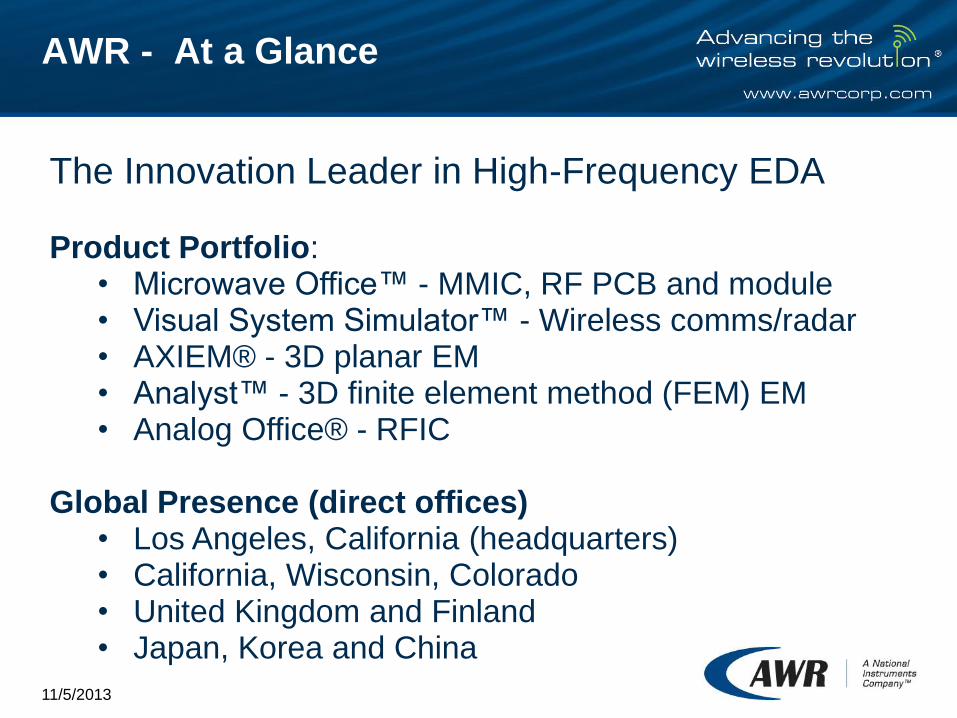
AWR - At a Glance
The Innovation Leader in High-Frequency EDA
Product Portfolio: • Microwave Office™ - MMIC, RF PCB and module • Visual System Simulator™ - Wireless comms/radar • AXIEM® - 3D planar EM • Analyst™ - 3D finite element method (FEM) EM • Analog Office® - RFIC
Global Presence (direct offices)
• Los Angeles, California (headquarters) • California, Wisconsin, Colorado • United Kingdom and Finland • Japan, Korea and China
11/5/2013
Page 4
Microwave Office
• MMIC
• RF PCB
• Modules
RF and Microwave Design Software
11/5/2013
Amplifier Technology Uses
Microwave Office to Design
High Performance Amplifiers
While Cutting 50% Off Their
Design Time
"Microwave Office has helped us
characterize appropriate parameters
for each prototype design, evaluate
possible variants and simulate the
device performance straight from the
design stage. In my experience
Microwave Office is the best design
solution available on the market."
Paul Deacon
Senior RF Design Engineer
Amplifier Technology
Page 5
11/5/2013
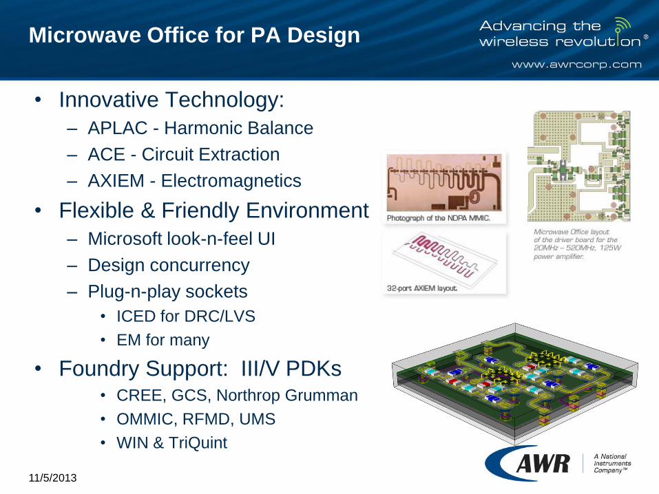
Microwave Office for PA Design
• Innovative Technology:
– APLAC - Harmonic Balance
– ACE - Circuit Extraction
– AXIEM - Electromagnetics
• Flexible & Friendly Environment
– Microsoft look-n-feel UI
– Design concurrency
– Plug-n-play sockets
• ICED for DRC/LVS
• EM for many
• Foundry Support: III/V PDKs • CREE, GCS, Northrop Grumman
• OMMIC, RFMD, UMS
• WIN & TriQuint
Page 6
Learn More…
Online:
• www.awrcorp.com
• AWR.TV
Communities:
• Facebook
• Twitter
• LinkedIn
• YouTube
Email:
• [email protected]
11/5/2013
Page 7
Cree: the World’s Largest Pure Play WBG Company
Overview
• Founded in 1987
• Public since 1993 (Nasdaq: CREE)
• Headquartered in Durham, NC
• Strong patent portfolio
Global Reach
• 12 major locations
• 6000 employees
• Fiscal 2013 Revenues $1.4B
25 Years of SiC and GaN wide bandgap wafer, epi and device experience.
Power & RFWBG Center of Excellence
pg. 7
Page 8
Cree businesses – a leading player in each sector
Cree
SiC/GaN
Materials
8
World record
LED efficacy
(lm/ W)
World ‘s first
commercial SiC
MOSFET
Award winning
commercial
lighting
Leader in GaN
RF Sales
Page 9
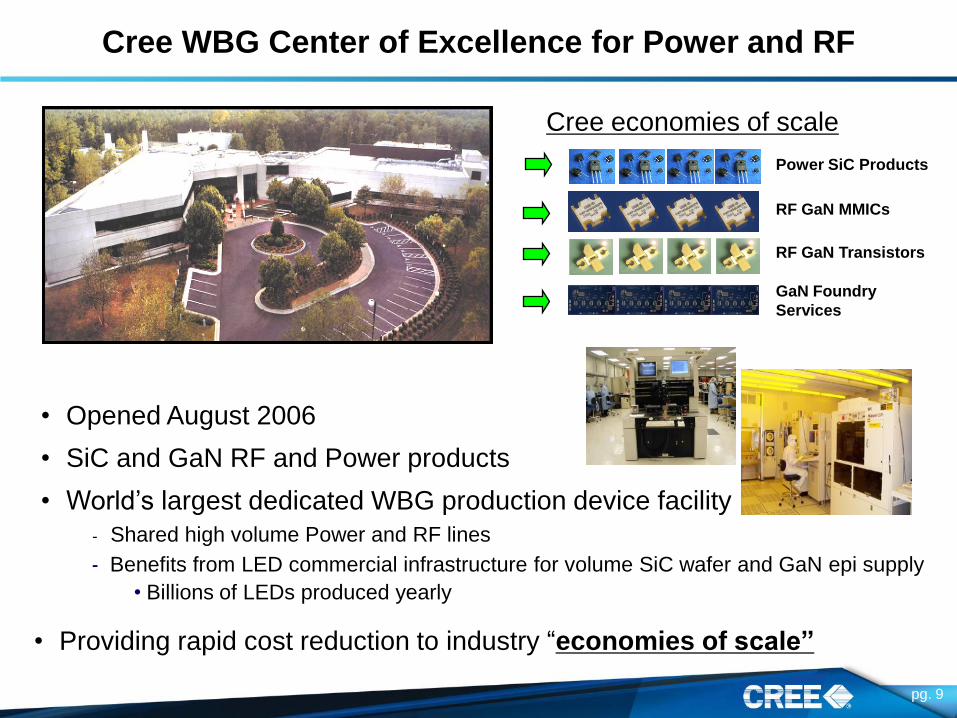
Cree WBG Center of Excellence for Power and RF
Power SiC Products
RF GaN MMICs
RF GaN Transistors
Cree economies of scale
• Opened August 2006
• SiC and GaN RF and Power products
• World’s largest dedicated WBG production device facility
GaN Foundry
Services
• Providing rapid cost reduction to industry “economies of scale”
- Benefits from LED commercial infrastructure for volume SiC wafer and GaN epi supply
• Billions of LEDs produced yearly
- Shared high volume Power and RF lines
pg. 9
Page 10
RF and Microwave Amplifier Power Added Efficiency, Fact and Fiction 2013, November 6th 10
RF and Microwave Amplifier Power
Added Efficiency, Fact and Fiction
Dr. Dominic FitzPatrick
Principal Consultant,
PoweRFul Microwave
www.powerful-microwave.co.uk
Page 11
RF and Microwave Amplifier Power Added Efficiency, Fact and Fiction 2013, November 6th 11
Power Added Efficiency
– The Basics
Why is it important?
Smaller power supply, less current drawn
Smaller, lighter DC supply cables
Less heat generated
Cooler running, higher reliability
Lower weight,
The higher the performance.
But, it doesn’t come for free; and it becomes harder to improve
the efficiency the higher we go, i.e. 10% increase from 30-40%
from 60-70% from 70-80%
Page 12
RF and Microwave Amplifier Power Added Efficiency, Fact and Fiction 2013, November 6th 12
Power Added Efficiency
– The Basics
What does the equation mean?
Note:- RFPIN means ‘IN’ to the device, not the source
power, i.e. better input match higher PAE?
Higher gain, higher PAE – GaN advantage!
Don’t get confused with Drain Efficiency.
Is DE actually a useful measure without including the
impact of gain?
Page 13
RF and Microwave Amplifier Power Added Efficiency, Fact and Fiction 2013, November 6th 13
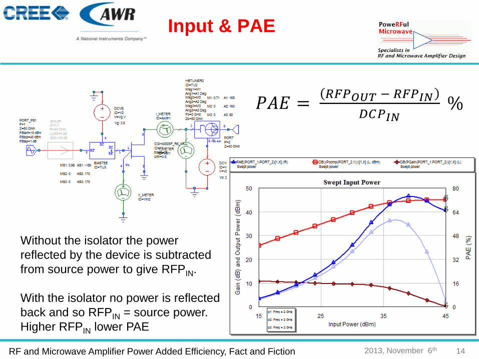
Input & PAE
With the isolator no power is reflected
back and so RFPIN = source power.
Higher RFPIN lower PAE
Page 14
RF and Microwave Amplifier Power Added Efficiency, Fact and Fiction 2013, November 6th 14
Input & PAE
Without the isolator the power
reflected by the device is subtracted
from source power to give RFPIN.
With the isolator no power is reflected
back and so RFPIN = source power.
Higher RFPIN lower PAE
Page 15
RF and Microwave Amplifier Power Added Efficiency, Fact and Fiction 2013, November 6th 16
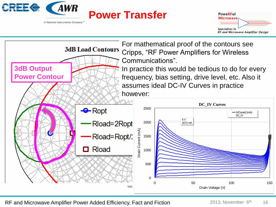
Power Transfer
We normally look at device impedances on the Smith Chart, and if we consider the
case of the maximum output load Ropt, there are also two load which will deliver half
the power (3dB down), Ropt/2 and Ropt x2
V
I
1 2
1 2
3
4
GPROBEID=XF1Rsense=0.0001 Ohm
PORTP=1Z=30 Ohm
PORTP=2Z=50 Ohm
PORTP=3Z=50 Ohm
PORTP=4Z=15 Ohm
0 1.0
1.0
-1.0
10.0
10.0
-10.0
5.0
5.0
-5.0
2.0
2.0
-2.0
3.0
3.0
-3.0
4.0
4.0
-4.0
0.2
0.2
-0.2
0.4
0.4
-0.4
0.6
0.6
-0.6
0.8
0.8
-0.8
Load Match
Swp Max
3GHz
Swp Min
1GHz
GAM1_GP(1,3,2,50,0)Device Output
GAM2_GP(4,3,2,50,0)Device Output
3dB Output
Power Contour
For mathematical proof of the contours see
Cripps, “RF Power Amplifiers for Wireless
Communications”.
In practice this would be tedious to do for every
frequency, bias setting, drive level, etc. Also it
assumes ideal DC-IV Curves in practice
however:
0 50 100 150
Drain Voltage (V)
DC_IV Curves
0
500
1000
1500
2000
2500
Dra
in C
urr
ent (m
A)
p16p15p14p13p12p11p10p9p8p7p6p5p4p3p2p1
6 V2072 mA
IVCurve() (mA)DC_IV
p1: Vstep = -3 V
p2: Vstep = -2.8 V
p3: Vstep = -2.6 V
p4: Vstep = -2.4 V
p5: Vstep = -2.2 V
p6: Vstep = -2 V
p7: Vstep = -1.8 V
p8: Vstep = -1.6 V
p9: Vstep = -1.4 V
p10: Vstep = -1.2 V
p11: Vstep = -1 V
p12: Vstep = -0.8 V
p13: Vstep = -0.6 V
p14: Vstep = -0.4 V
p15: Vstep = -0.2 V
p16: Vstep = 0 V
Page 16
RF and Microwave Amplifier Power Added Efficiency, Fact and Fiction 2013, November 6th 17
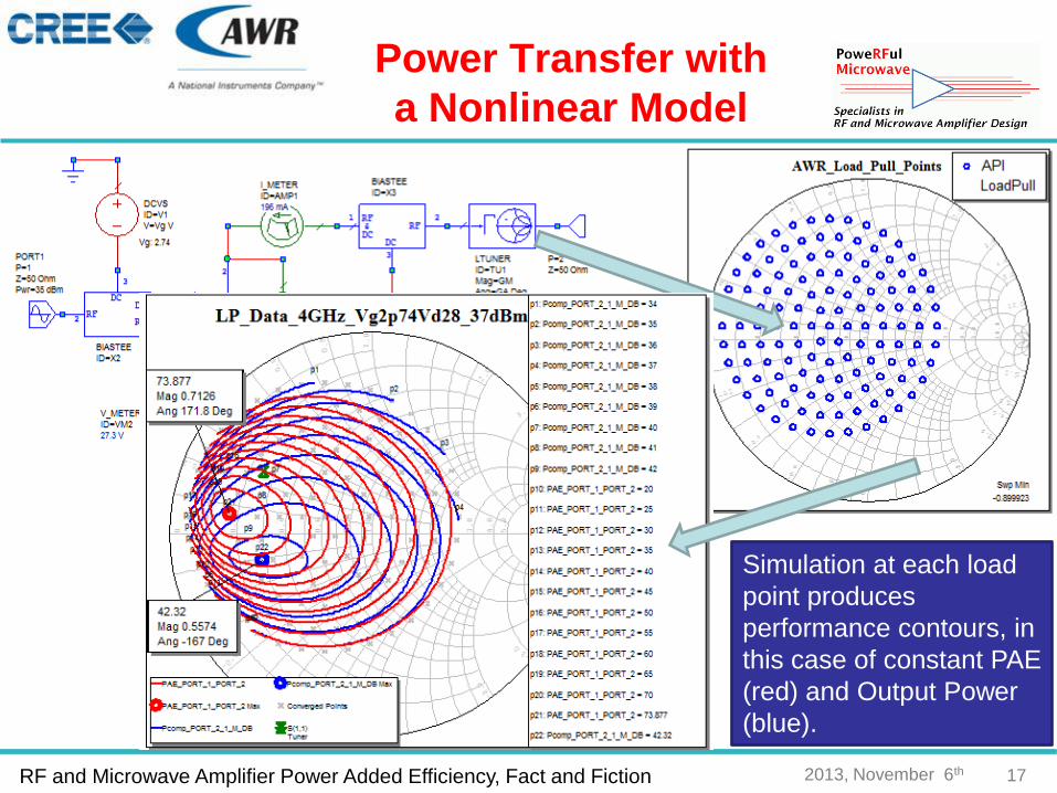
Power Transfer with
a Nonlinear Model
Tuner steps over
impedance grid.
Simulation at each load
point produces
performance contours, in
this case of constant PAE
(red) and Output Power
(blue).
Page 17
RF and Microwave Amplifier Power Added Efficiency, Fact and Fiction 2013, November 6th 18
Bias
Not going to cover the theory of different classes of operation
here
→ Already comprehensively covered such as by Prof. Steve
Cripps.
But we will look at the effects of bias and remember that it is
another variable open to use.
Available (Power) Gain at Vp
(bold), Idq=200mA and Idq=800mA
Page 18
RF and Microwave Amplifier Power Added Efficiency, Fact and Fiction 2013, November 6th 19
Bias
Not going to cover the theory of different classes of operation
here
→ Already comprehensively covered such as by Prof. Steve
Cripps.
But we will look at the effects of bias and remember that it is
another variable open to use.
Increase
Thermal
Resistance
to 8°C/W
Thermal Optimization of GaN HEMT
Transistor Power Amplifiers Using New Self-
heating Large Signal Model, Cree-App-Note-
006
Page 19
RF and Microwave Amplifier Power Added Efficiency, Fact and Fiction 2013, November 6th 20
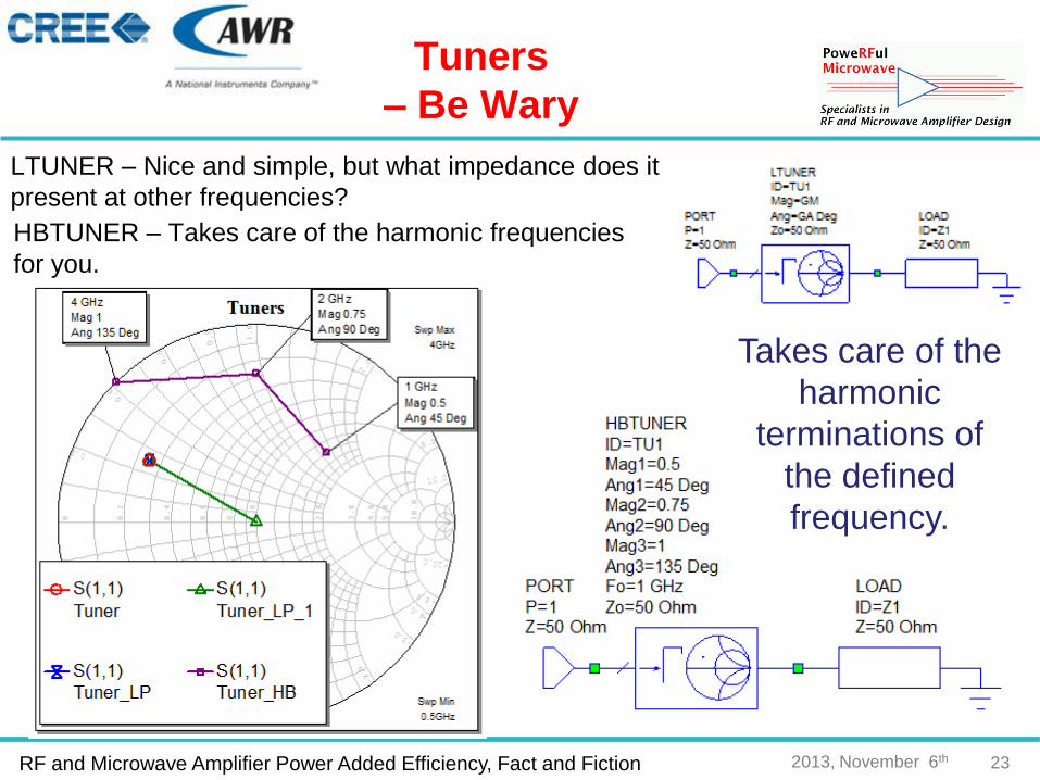
Tuners
– Be Wary
LTUNER – Nice and simple, but what impedance does it
present at other frequencies?
LTUNER – All frequencies are terminated with the same
load impedance, in this case |GM| /_GA°.
Page 20
RF and Microwave Amplifier Power Added Efficiency, Fact and Fiction 2013, November 6th 21
Tuners
– Be Wary
LTUNER – Nice and simple, but what impedance does it
present at other frequencies?
LTUNER – All frequencies are terminated with the same
load impedance.
LPTUNER – Define frequencies and their terminations,
but if you don’t define them they default.
Here we have defined 0.5, 1 &
2GHz but the other frequencies
2.5, 3, 3.5 and 4GHz also have
defaulted to this load.
Page 21
RF and Microwave Amplifier Power Added Efficiency, Fact and Fiction 2013, November 6th 22
Tuners
– Be Wary
LTUNER – Nice and simple, but what impedance does it
present at other frequencies?
LTUNER – All frequencies are terminated with the same
load impedance.
LPTUNER – Define frequencies and their terminations,
but if you don’t define them they default.
Now we have defined
different impedances to
some of the frequencies, 3 &
4GHz are terminated in 50Ω
Page 22
RF and Microwave Amplifier Power Added Efficiency, Fact and Fiction 2013, November 6th 23
Tuners
– Be Wary
LTUNER – Nice and simple, but what impedance does it
present at other frequencies?
LTUNER – All frequencies are terminated with the same
load impedance.
HBTUNER – Takes care of the harmonic frequencies
for you.
Takes care of the
harmonic
terminations of
the defined
frequency.
Page 23
RF and Microwave Amplifier Power Added Efficiency, Fact and Fiction 2013, November 6th 24
Tuners
– Be Wary
LTUNER – Nice and simple, but what impedance does it
present at other frequencies?
LTUNER – All frequencies are terminated with the same
load impedance.
HBTUNER – But…. Be aware of what happens at other
frequencies and their terminations.
Harmonic impedance has
an impact on device
performance, so know
where you have put yours!
Page 24
RF and Microwave Amplifier Power Added Efficiency, Fact and Fiction 2013, November 6th 25
Load Pull Set Up
Difference between using LTUNER and HBTUNER with
harmonics terminated in 50Ω.
Load Pull with LTUNER Load Pull with HBTUNER
Small impact on Pout – Significant on PAE
Page 25
RF and Microwave Amplifier Power Added Efficiency, Fact and Fiction 2013, November 6th 26
Load Pull Set Up
We use Load Pull so that we can visualise the trade-
offs between parameters, typically PAE and Pout.
Load Pull Check List 1. Harmonic terminations –
use HBTUNER for
accurate/consistent results.
2. Input Power level, check
that you are using the
optimum drive level by
conducting a power sweep.
3. Bias/Class of operation.
Page 26
RF and Microwave Amplifier Power Added Efficiency, Fact and Fiction 2013, November 6th 27
Input Match Effects
Why does the input match
change?
1. Intrinsic capacitance
2. Channel resistance
3. Load match
Intrinsic Cree GaN HEMT Models allow more accurate
waveform engineered PA designs
Ray Pengelly and Bill Pribble, Cree RF Products
ARMMS, April, 2013
Page 27
RF and Microwave Amplifier Power Added Efficiency, Fact and Fiction 2013, November 6th 28
Effect of Load on
Input Match
33dBm
Page 28
RF and Microwave Amplifier Power Added Efficiency, Fact and Fiction 2013, November 6th 29
Effect of Load on
Input Match
33dBm
Page 29
RF and Microwave Amplifier Power Added Efficiency, Fact and Fiction 2013, November 6th 30
Effect of Load
on Input Match
33dBm
Page 30
RF and Microwave Amplifier Power Added Efficiency, Fact and Fiction 2013, November 6th 31
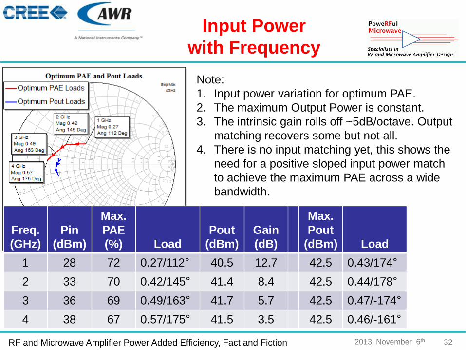
Input Power
with Frequency
For wideband designs you have to
consider input power vs. frequency.
Output power stays ~ constant with
frequency.
So, to a first order input power needs to
increase at this rate.
Let’s take a look
6dB/octave slope
Page 31
RF and Microwave Amplifier Power Added Efficiency, Fact and Fiction 2013, November 6th 32
Input Power
with Frequency
Freq.
(GHz)
Pin
(dBm)
Max.
PAE
(%) Load
Pout
(dBm)
Gain
(dB)
Max.
Pout
(dBm) Load
1 28 72 0.27/112° 40.5 12.7 42.5 0.43/174°
2 33 70 0.42/145° 41.4 8.4 42.5 0.44/178°
3 36 69 0.49/163° 41.7 5.7 42.5 0.47/-174°
4 38 67 0.57/175° 41.5 3.5 42.5 0.46/-161°
Note:
1. Input power variation for optimum PAE.
2. The maximum Output Power is constant.
3. The intrinsic gain rolls off ~5dB/octave. Output
matching recovers some but not all.
4. There is no input matching yet, this shows the
need for a positive sloped input power match
to achieve the maximum PAE across a wide
bandwidth.
Page 32
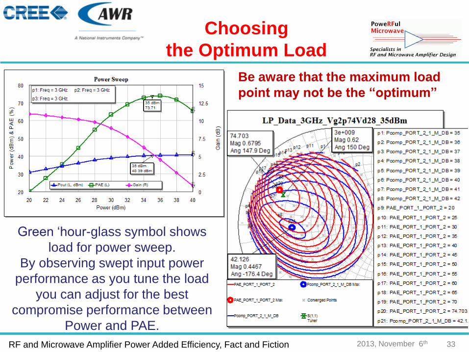
RF and Microwave Amplifier Power Added Efficiency, Fact and Fiction 2013, November 6th 33
Choosing
the Optimum Load
For wideband designs you have to
consider input power vs. frequency.
Output power stays ~ constant with
frequency.
So, to a first order input power needs to
increase at this rate.
Let’s take a look
Green ‘hour-glass symbol shows
load for power sweep.
By observing swept input power
performance as you tune the load
you can adjust for the best
compromise performance between
Power and PAE.
Be aware that the maximum load
point may not be the “optimum”
Page 33
RF and Microwave Amplifier Power Added Efficiency, Fact and Fiction 2013, November 6th 34
Returning to
the Optimum Loads
Looking at a simple device
output equivalent circuit,
including some package de-
embedding:
The equivalent load
resistance increases from
23Ω for the optimum power
loads to 41Ω for the
optimum PAE loads – which
agrees with theory Device Package
Page 34
RF and Microwave Amplifier Power Added Efficiency, Fact and Fiction 2013, November 6th 35
Load Line Theory
Class A Bias
Point
Class A/B Bias
Point
Theory Optimum Power load = 2x(VD-VK)/IDS = 20Ω
Page 35
RF and Microwave Amplifier Power Added Efficiency, Fact and Fiction 2013, November 6th 36
Load Line Simulation
Addition of internal nodes to
model allows direct observation
of drain waveforms.
As we increase drive Dynamic (RF) load
line interacts with limits of the DC-IV
envelope.
Page 36
RF and Microwave Amplifier Power Added Efficiency, Fact and Fiction 2013, November 6th 37
Load Line Simulation
Addition of internal nodes to
model allows direct observation
of drain waveforms. Or change load impedance
Page 37
RF and Microwave Amplifier Power Added Efficiency, Fact and Fiction 2013, November 6th 38
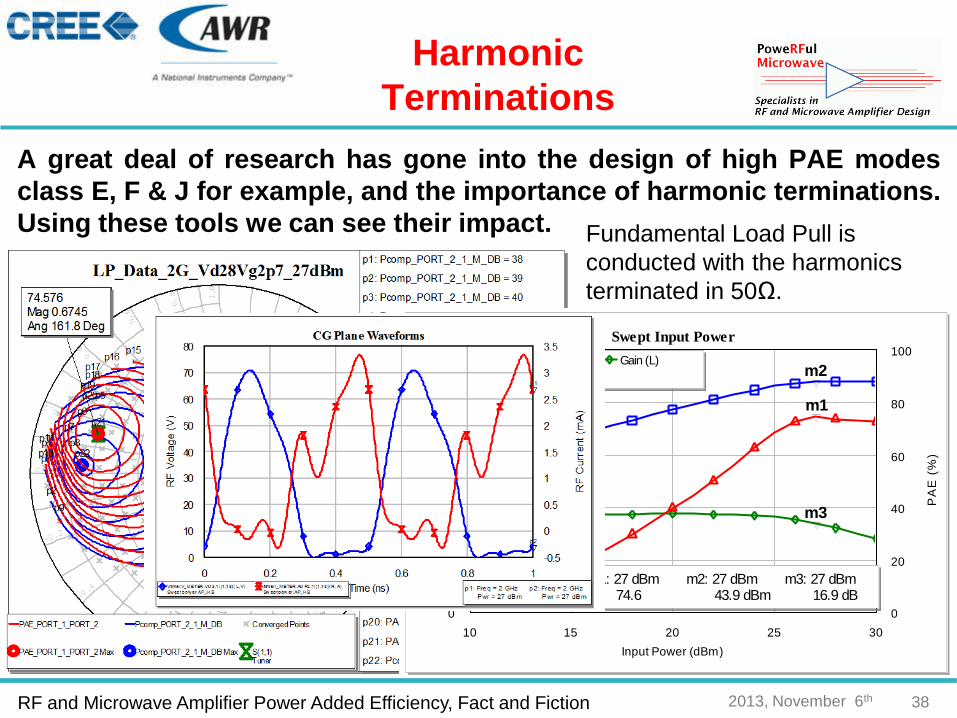
Harmonic
Terminations
A great deal of research has gone into the design of high PAE modes
class E, F & J for example, and the importance of harmonic terminations.
Using these tools we can see their impact. Fundamental Load Pull is
conducted with the harmonics
terminated in 50Ω.
10 15 20 25 30
Input Power (dBm)
Swept Input Power
0
10
20
30
40
50
Ga
in (
dB
) a
nd
Ou
tpu
t P
ow
er
(dB
m)
0
20
40
60
80
100
PA
E (
%)
m3
m2
m1
PAE (R)
Pout (L, dBm)
Gain (L)
m1: 27 dBm74.6
m2: 27 dBm43.9 dBm
m3: 27 dBm16.9 dB
Page 38
RF and Microwave Amplifier Power Added Efficiency, Fact and Fiction 2013, November 6th 39
Harmonic
Terminations
Keeping the Fundamental at the optimum PAE impedance a 2nd Harmonic Load
Pull is conducted with the 3r harmonic terminated in 50Ω. We are simulating across
the majority of the real
impedance plane. Of
interest is not just the
optima but also the minima
– places to avoid!
Page 39
RF and Microwave Amplifier Power Added Efficiency, Fact and Fiction 2013, November 6th 40
Harmonic
Terminations
Keeping the Fundamental & now 2nd at their optimum PAE impedances a 3rd
Harmonic Load Pull is conducted. We now have almost half
the impedance plane where
the effect is minimal
however we again see
where to avoid!.
10 15 20 25 30
Input Power (dBm)
Swept Input Power
0
10
20
30
40
50
Ga
in (
dB
) a
nd
Ou
tpu
t P
ow
er
(dB
m)
0
20
40
60
80
100
PA
E (
%)
m3
m2m1
PAE (R)
Pout (L, dBm)
Gain (L)
m1: 27 dBm82.8
m2: 27 dBm44.4 dBm
m3: 27 dBm17.4 dB
Page 40
RF and Microwave Amplifier Power Added Efficiency, Fact and Fiction 2013, November 6th 41
Harmonic
Terminations
Now we have all our terminations optimised, or have we? Re-do the
fundamental load pull with the optimum PAE harmonic terminations -
The fundamental load has
moved and we have increased
the maximum PAE.
0 0.2 0.4 0.6 0.8 1
Time (ns)
CG Plane Waveforms
0
10
20
30
40
50
60
70
80
RF
Vo
lta
ge
(V
)
-0.5
0
0.5
1
1.5
2
2.5
3
3.5
RF
Cu
rre
nt
(mA
)
p2
p1
Vtime(V_METER.VM3,1)[1,18] (L, V)
Swept power.AP_HB
Itime(I_METER.AMP2,1)[1,18] (R, A)
Swept power.AP_HBp1: Freq = 2 GHz
Pwr = 27 dBmp2: Freq = 2 GHz
Pwr = 27 dBm
Page 41
RF and Microwave Amplifier Power Added Efficiency, Fact and Fiction 2013, November 6th 42
Harmonic
Terminations
No significant change at
30% PAE and 40dBm
Pout, but increase in the
peaks and consequently a
wider impedance range
included in the 70% PAE
and 45dBm Pout, indeed
these two regions now
have a significant overlap.
Page 42
RF and Microwave Amplifier Power Added Efficiency, Fact and Fiction 2013, November 6th 43
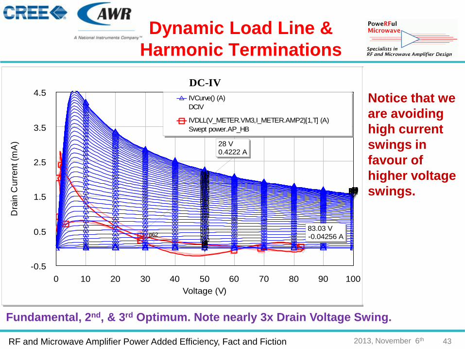
Dynamic Load Line &
Harmonic Terminations
Fundamental Optimum, 2nd & 3rd in 50Ω
0 10 20 30 40 50 60 70 80 90 100
Voltage (V)
DC-IV
-0.5
0.5
1.5
2.5
3.5
4.5
Dra
in C
urr
ent
(mA
)
p62
p61p60p59p58p57p56p55p54p53p52p51p50p49p48p47p46p45p44p43p42
p41p40p39p38p37p36p35p34p33p32p31p30p29p28p27p26p25p24p23p22p21p20p19p18p17p16p15p14p13p12p11p10p9p8p7p6p5p4p3p2p1
28 V0.4222 A
IVCurve() (A)
DCIV
IVDLL(V_METER.VM3,I_METER.AMP2)[1,T] (A)
Swept power.AP_HB
p1: Vstep = -4 V p2: Vstep = -3.9 V p3: Vstep = -3.8 V
p4: Vstep = -3.7 V p5: Vstep = -3.6 V p6: Vstep = -3.5 V
p7: Vstep = -3.4 V p8: Vstep = -3.3 V p9: Vstep = -3.2 V
p10: Vstep = -3.1 V p11: Vstep = -3 V p12: Vstep = -2.9 V
p13: Vstep = -2.8 V p14: Vstep = -2.7 V p15: Vstep = -2.6 V
p16: Vstep = -2.5 V p17: Vstep = -2.4 V p18: Vstep = -2.3 V
p19: Vstep = -2.2 V p20: Vstep = -2.1 V p21: Vstep = -2 V
p22: Vstep = -1.9 V p23: Vstep = -1.8 V p24: Vstep = -1.7 V
p25: Vstep = -1.6 V p26: Vstep = -1.5 V p27: Vstep = -1.4 V
p28: Vstep = -1.3 V p29: Vstep = -1.2 V p30: Vstep = -1.1 V
p31: Vstep = -1 V p32: Vstep = -0.9 V p33: Vstep = -0.8 V
p34: Vstep = -0.7 V p35: Vstep = -0.6 V p36: Vstep = -0.5 V
p37: Vstep = -0.4 V p38: Vstep = -0.3 V p39: Vstep = -0.2 V
p40: Vstep = -0.1 V p41: Vstep = 0 V p42: Vstep = 0.1 V
p43: Vstep = 0.2 V p44: Vstep = 0.3 V p45: Vstep = 0.4 V
p46: Vstep = 0.5 V p47: Vstep = 0.6 V p48: Vstep = 0.7 V
p49: Vstep = 0.8 V p50: Vstep = 0.9 V p51: Vstep = 1 V
p52: Vstep = 1.1 V p53: Vstep = 1.2 V p54: Vstep = 1.3 V
p55: Vstep = 1.4 V p56: Vstep = 1.5 V p57: Vstep = 1.6 V
p58: Vstep = 1.7 V p59: Vstep = 1.8 V p60: Vstep = 1.9 V
p61: Vstep = 2 V p62: Freq = 2 GHzPwr = 27 dBm
Fundamental & 2nd Optimum, 3rd in 50Ω
0 10 20 30 40 50 60 70 80 90 100
Voltage (V)
DC-IV
-0.5
0.5
1.5
2.5
3.5
4.5
Dra
in C
urr
ent
(mA
)
p62
p61p60p59p58p57p56p55p54p53p52p51p50p49p48p47p46p45p44p43p42
p41p40p39p38p37p36p35p34p33p32p31p30p29p28p27p26p25p24p23p22p21p20p19p18p17p16p15p14p13p12p11p10p9p8p7p6p5p4p3p2p1
83.03 V-0.04256 A
28 V0.4222 A
IVCurve() (A)
DCIV
IVDLL(V_METER.VM3,I_METER.AMP2)[1,T] (A)
Swept power.AP_HB
p1: Vstep = -4 V p2: Vstep = -3.9 V p3: Vstep = -3.8 V
p4: Vstep = -3.7 V p5: Vstep = -3.6 V p6: Vstep = -3.5 V
p7: Vstep = -3.4 V p8: Vstep = -3.3 V p9: Vstep = -3.2 V
p10: Vstep = -3.1 V p11: Vstep = -3 V p12: Vstep = -2.9 V
p13: Vstep = -2.8 V p14: Vstep = -2.7 V p15: Vstep = -2.6 V
p16: Vstep = -2.5 V p17: Vstep = -2.4 V p18: Vstep = -2.3 V
p19: Vstep = -2.2 V p20: Vstep = -2.1 V p21: Vstep = -2 V
p22: Vstep = -1.9 V p23: Vstep = -1.8 V p24: Vstep = -1.7 V
p25: Vstep = -1.6 V p26: Vstep = -1.5 V p27: Vstep = -1.4 V
p28: Vstep = -1.3 V p29: Vstep = -1.2 V p30: Vstep = -1.1 V
p31: Vstep = -1 V p32: Vstep = -0.9 V p33: Vstep = -0.8 V
p34: Vstep = -0.7 V p35: Vstep = -0.6 V p36: Vstep = -0.5 V
p37: Vstep = -0.4 V p38: Vstep = -0.3 V p39: Vstep = -0.2 V
p40: Vstep = -0.1 V p41: Vstep = 0 V p42: Vstep = 0.1 V
p43: Vstep = 0.2 V p44: Vstep = 0.3 V p45: Vstep = 0.4 V
p46: Vstep = 0.5 V p47: Vstep = 0.6 V p48: Vstep = 0.7 V
p49: Vstep = 0.8 V p50: Vstep = 0.9 V p51: Vstep = 1 V
p52: Vstep = 1.1 V p53: Vstep = 1.2 V p54: Vstep = 1.3 V
p55: Vstep = 1.4 V p56: Vstep = 1.5 V p57: Vstep = 1.6 V
p58: Vstep = 1.7 V p59: Vstep = 1.8 V p60: Vstep = 1.9 V
p61: Vstep = 2 V p62: Freq = 2 GHzPwr = 27 dBm
Fundamental, 2nd, & 3rd Optimum. Note nearly 3x Drain Voltage Swing.
Notice that we
are avoiding
high current
swings in
favour of
higher voltage
swings.
Page 43
RF and Microwave Amplifier Power Added Efficiency, Fact and Fiction 2013, November 6th 44
Optimum Load Design
is a Cyclical Process
Harmonic Load Pull Steps:
1. Optimum Fundamental Drive
Power.
2. Optimum Fundamental Load -
Check (1) is still true.
3. 2nd Harmonic LP – Check (1) & (2)
are still true.
4. 3rd Harmonic LP –Check (1), (2)
and (3) are still true.
5. Go on to next frequency!
Remember it is not only
about finding the
optimums - you also need
to know where to avoid!
We can’t always use the optimum
harmonic termination. If we are
doing wide bandwidth designs
the harmonic falls in band.
Page 44
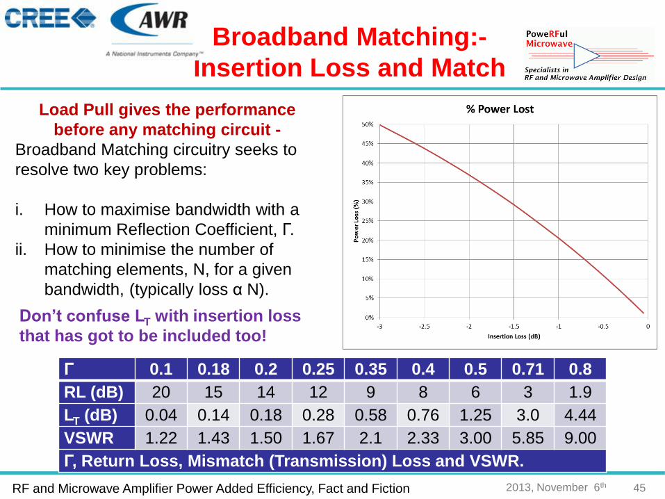
RF and Microwave Amplifier Power Added Efficiency, Fact and Fiction 2013, November 6th 45
Broadband Matching:-
Insertion Loss and Match
Γ 0.1 0.18 0.2 0.25 0.35 0.4 0.5 0.71 0.8
RL (dB) 20 15 14 12 9 8 6 3 1.9
LT (dB) 0.04 0.14 0.18 0.28 0.58 0.76 1.25 3.0 4.44
VSWR 1.22 1.43 1.50 1.67 2.1 2.33 3.00 5.85 9.00
Γ, Return Loss, Mismatch (Transmission) Loss and VSWR.
Load Pull gives the performance
before any matching circuit -
Broadband Matching circuitry seeks to
resolve two key problems:
i. How to maximise bandwidth with a
minimum Reflection Coefficient, Γ.
ii. How to minimise the number of
matching elements, N, for a given
bandwidth, (typically loss α N).
Don’t confuse LT with insertion loss
that has got to be included too!
Page 45
RF and Microwave Amplifier Power Added Efficiency, Fact and Fiction 2013, November 6th 46
Current Approaches
and Performance
Page 46
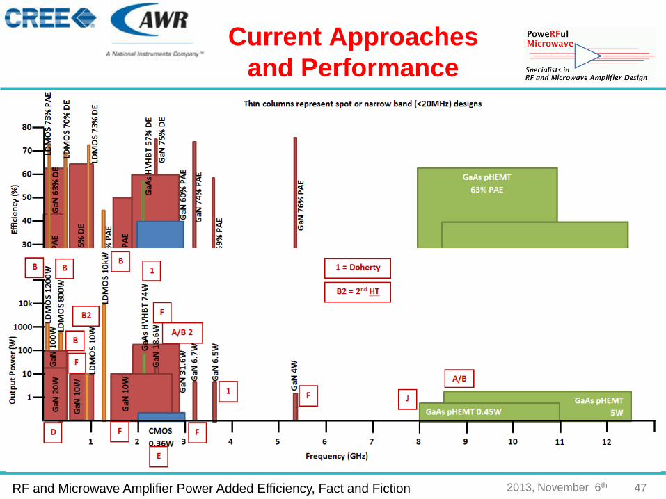
RF and Microwave Amplifier Power Added Efficiency, Fact and Fiction 2013, November 6th 47
Current Approaches
and Performance
Page 47
RF and Microwave Amplifier Power Added Efficiency, Fact and Fiction 2013, November 6th 48
Current Approaches
and Performance
Technology Class Fmin GHz
Fmax GHz
Eff. % Pout Dev.Power Year Reference
cmos E 2 3 40.2 PAE 0.36 NS 2013 Broadband and High-Efficiency Power Amplifier that Integrates CMOS and IPD Technology
GaAs pHEMT A/B 8.5 12.5 40 PAE 5 8x 0.8 2013 Design Procedure 4 Hi-Eff and Compact-Size 5–10W MMIC PAs in GaAs pHEMT Tech.
GaN HEMT F 5.65 5.7 76 PAE 4 0.96mm 2012 Ultra High Efficiency Microwave Power Amplifier for Wireless Power Transmission
GaN HEMT F-1 3.27 3.3 74 PAE 6.7 10 2010 First-Pass Design of High Efficiency Power Amplifiers using Accurate Large Signal Models
GaN HEMT F-1 PushPull 2.5 2.55 75 DE 18.6 2x 10 2010 First-Pass Design of High Efficiency Power Amplifiers using Accurate Large Signal Models
GaAs pHEMT J 8 11 63 DE 0.45 0.6 2011 GaAs X-Band Hi Eff (>65%) Broadband (>30%) Amp MMIC based on Class B to J Continuum
GaAs HVHBT Doherty 2.1 2.15 57 DE 74 2x 120 2010 Doherty Power Amp using 2nd Gen. HVHBT Technology for Hi Eff Basestation Applications
LDMOS B 2HT 0.9 0.95 73 DE 10 30 2010 Lumped-element Output Networks for High-efficiency Power Amplifiers
GaN HEMT B? 0.01 0.5 43 PAE 100 4x 45 2009 Design of a 100Watt High-Efficiency Power Amplifier for the 10-500MHz Band
GaN HEMT VM D 0.05 0.5 63 DE 20 10 x2 2011 Development of a WB Highly Efficient GaN VoltageModeClassD VHFUHF Power Amplifier
GaN HEMT Doherty 3.5 3.55 59 PAE 6.5 6 x2 2013 A LinearandEfficientDohertyPAat3p5GHz
GaN HEMT F 0.55 1.1 65 DE 10 10 2011 A Novel Hi Eff BB Continuous ClassF RFPA Delivering 74% Average Eff for an Octave BW
GaN HEMT A/B 2HT 1.9 2.9 60 DE 31.6 45 2010 Design of a BB Highly Efficient 45W GaN PA via Simplified Real Freq Technique
GaN HEMT J 1.4 2.7 50 PAE 10 10 2009 Methodology4RealizingHiEffClassJinaLinearBroadbandPA
LDMOS B 0.5 0.505 66 PAE 680 1000 2012 Developments of High CW RF PowerSSAatSoleil
LDMOS B 1.3 1.305 45 PAE 10000 160 2012 1st Experience At Elbe with new 1.3GHz CWRF System Based on 10kWSSA
LDMOS B 0.085 0.115 73 PAE 1200 1200 2012 Own work
Recommend Cree Website for extensive list of technical papers:
http://www.cree.com/RF/Document-Library
Page 48
RF and Microwave Amplifier Power Added Efficiency, Fact and Fiction 2013, November 6th 49
Topology Counts
Balanced Approach: A number of the papers just referenced used balanced amplifiers to achieve
high power and efficiency, particularly the very high power LDMOS. Two
GaN exceptions were the broad band “Design of a 100Watt High-Efficiency
Power Amplifier for the 10-500MHz Band” (left) and the 2.5GHz “First-Pass
Design of High Efficiency Power Amplifiers using Accurate Large Signal
Models” (right). Interesting both use devices capable of 2x the output power
they achieve.
Page 49
RF and Microwave Amplifier Power Added Efficiency, Fact and Fiction 2013, November 6th 50
Topology Counts
Doherty Approach: Uses parallel devices to increase efficiency
at back off as graph from “Doherty Power
Amplifiers using 2nd Generation HVHBT
Technology for High Efficiency Basestation
Applications”.
Astrium 200W GaN demonstrator performance
using drain bias adjustment for increased PAE.
Envelope Tracking
Page 50
RF and Microwave Amplifier Power Added Efficiency, Fact and Fiction 2013, November 6th 51
Summary
a) Device self-heating model.
b) Input match.
c) Wide Band designs ‘tapered’ input drive level.
d) Observe the Current Generator Plane waveforms –
6 port device model.
e) Don’t forget mismatch and insertion losses of
output matching circuit.
f) Harmonic terminations - they can both enhance
and degrade performance.
g) Models aren’t valid over an infinite range.
Page 51
RF and Microwave Amplifier Power Added Efficiency, Fact and Fiction 2013, November 6th 52
Thank You!
Sponsored by:
www.awrcorp.com
www.cree.com
PoweRFul Microwave
www.powerful-microwave.co.uk
Questions?