RF circuits designGrzegorz BeziukGrzegorz Beziuk
RF characteristics of lumped passive and active elements
References[1] Tietze U., Schenk C., Electronic circuits : handbook for design and application, Springer
2008
[2] Golio M., RF and microwave passive and active technologies in: RF and Microwave
handbook, 2008, CRC Press Taylor and Francis Group
[3] Vishay, 50 GHz Thin Film Microwave Resistors, Products Data Sheet, Vishay 2009,
(www.vishay.com)
[4] AVX RF, AVX RF/Microwave products version 8.1, Products Data Sheet,
(www.avxrf.com)
[5] Panasonic, Chip inductors, Products Data Sheet,
(http://www.panasonic.com/industrial/electronic-components/inductive-products/chip-
inductors.aspx)
[6] Vishay semicondutors, BFR 93 - Silicon NPN Planar RF Transistor, Product Data Sheet,
2000, Vishay.
[7] NXP Semiconductors, BFU725F/N1 NPN wideband silicon germanium RF transistor,
Product Data Sheet, 2009, NXP Semiconductors (www.nxp.com)
References[8] Infineon Technologies, BFP 620 NPN Silicon Germanium RF Transistor, Product Data Sheet,
2004, Infineon Technologies (http//www.infineon.com/silicondiscretes)
[9] ON Semiconductors, MMBFU310LT1G JFET Transistor N−Channel, Product Data Sheet, 2009, ON
Semiconductors (www.onsemi.com)
[10] EPCOS, SAW Components, Data Sheet R 850, 2002, EPCOS, (www.epcos.com)
[11] Fabian Wai Lee Kung, RF/Microwave Circuit Design, 2008, Multimedia University, (open source
lectures: http://pesona.mmu.edu.my/~wlkung/ADS/ads.htm)
[12] Microsemi, KV1911A – KV1991A VARACTOR DIODES UHF Microwave Super-Hyperabrupt
Junction, 2007, Products Data Sheet, Microsemi
[13] Hawlett Packard, Surface mount microwave Schottky detector diodes HSMS 2850, HSMS 2860
series, Technical data, Hawlett Packard
[14] Maccom Technology Solutions, MA4AGBLP912 AlGaAs Beamlead PIN Diode, Products Data
Sheet, Maccom Technology Solutions
[15] Vishay Telefunken, BF966S N–Channel Dual Gate MOS-Fieldeffect Tetrode, Depletion Mode,
Product Data Sheet, 1999, Vishay Telefunken
[16] Murata Manufacturing, SAW resonators, Products Data Sheet, 2001, Murata Manufacturing
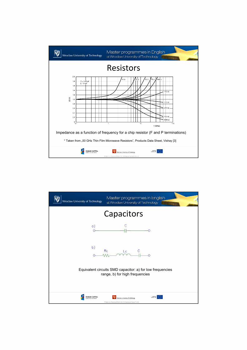
Resistors
Equivalent circuits SMD resistor: a) for low frequencies
range, b) for high frequencies
Resistors
( ) ( )[ ]( ) 22222
232
1 RCCL
CLRCLjRjZ
RRR
RRRRR
ωω
ωωω
+−
−−+=
Inductive properties:
Capacitive properties:
RR CLR /<
RR CLR />
Reflection factor: ( ) ( )( ) 0
0
ZjZ
ZjZj
R
RR
+
−=Γ
ω
ωω
Resistors
Impedance of SMD
resistors od the size 1206
with LR = 3nH, CR = 0.2pF
* Taken from „Electronic circuits : handbook for design and application” Tietze U., Schenk C. [1]
Resistors
Typical very high frequency performance electrical model
The external reactance (Lc and CG) depends on the PCB material, the layout and
assembly technology.
Resistors
Impedance as a function of frequency for a chip resistor N termination (wraparound)
* Taken from „50 GHz Thin Film Microwave Resistors”, Products Data Sheet, Vishay [3]
Resistors
Impedance as a function of frequency for a chip resistor (F and P terminations)
* Taken from „50 GHz Thin Film Microwave Resistors”, Products Data Sheet, Vishay [3]
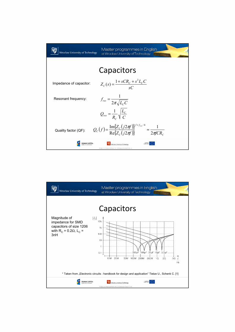
Capacitors
Equivalent circuits SMD capacitor: a) for low frequencies
range, b) for high frequencies
Capacitors
sC
CLssCRsZ CC
C
21)(
++=
C
L
RQ
CLf
C
C
res
C
res
1
2
1
=
=π
( ) ( ) ( ) C
ff
C
CC
fCRfjZ
fjZfQ
res
ππ
π
2
1
2Re
2Im4/
≈=<
Impedance of capacitor:
Resonant frequency:
Quality factor (QF):
CapacitorsMagnitude of
impedance for SMD
capacitors of size 1206
with RC = 0.2Ω, LC =
3nH
* Taken from „Electronic circuits : handbook for design and application” Tietze U., Schenk C. [1]
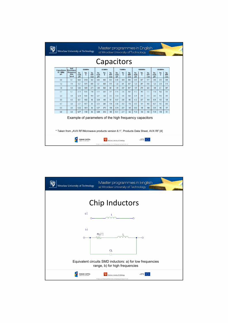
Capacitors
* Taken from „AVX RF/Microwave products version 8.1”, Products Data Sheet, AVX RF [4]
Example of parameters of the high frequency capacitors
Chip Inductors
Equivalent circuits SMD inductors: a) for low frequencies
range, b) for high frequencies
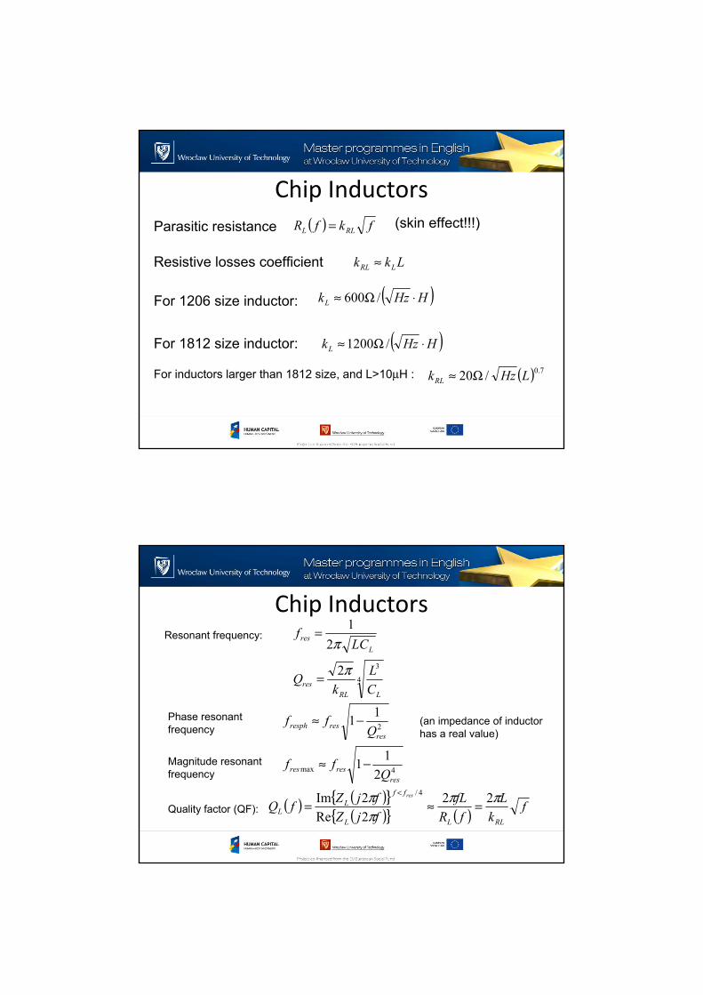
Chip Inductors
( ) fkfR RLL =
Lkk LRL ≈
( )HHzkL ⋅Ω≈ /1200
( )HHzkL ⋅Ω≈ /600
(skin effect!!!)Parasitic resistance
Resistive losses coefficient
For 1206 size inductor:
For 1812 size inductor:
For inductors larger than 1812 size, and L>10µH : ( ) 7.0/20 LHzkRL Ω≈
Chip Inductors
4
32
2
1
LRL
res
L
res
C
L
kQ
LCf
π
π
=
=
4max
2
2
11
11
res
resres
res
resresph
Qff
Qff
−≈
−≈
Resonant frequency:
Phase resonant
frequency
Magnitude resonant
frequency
(an impedance of inductor
has a real value)
Quality factor (QF): ( ) ( ) ( ) ( )
fk
L
fR
fL
fjZ
fjZfQ
RLL
ff
L
LL
res ππ
π
π 22
2Re
2Im4/
=≈=<
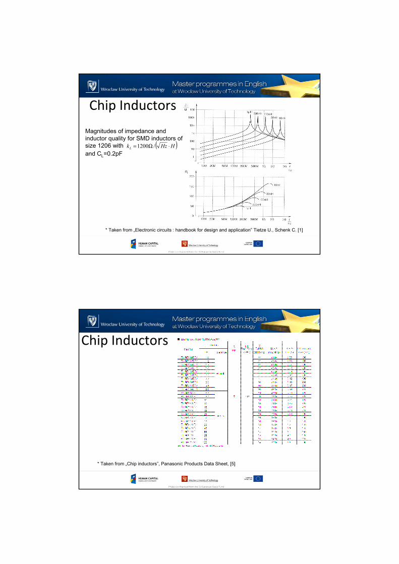
Chip Inductors
* Taken from „Electronic circuits : handbook for design and application” Tietze U., Schenk C. [1]
Magnitudes of impedance and
inductor quality for SMD inductors of
size 1206 with ( )HHzkL ⋅Ω= /1200
and CL=0.2pF
Chip Inductors
* Taken from „Chip inductors”, Panasonic Products Data Sheet, [5]
Chip Inductors
* Taken from „Chip inductors”, Panasonic Products Data Sheet, [5]
ChokesChoke is a kind of inductor. Chokes are used below 2 GHz,
but there are some chokes applications extends to tens of
GHz.
Chokes:
- for high frequency are high impedance elements
- for low frequency and direct current have very little loss
Chockes are use in the bias circuits of active elements.
Because the choke is an inductors with ferrite core, for high
frequency (f>2GHz) its resonances are absorbed by losses in
a ferrite.
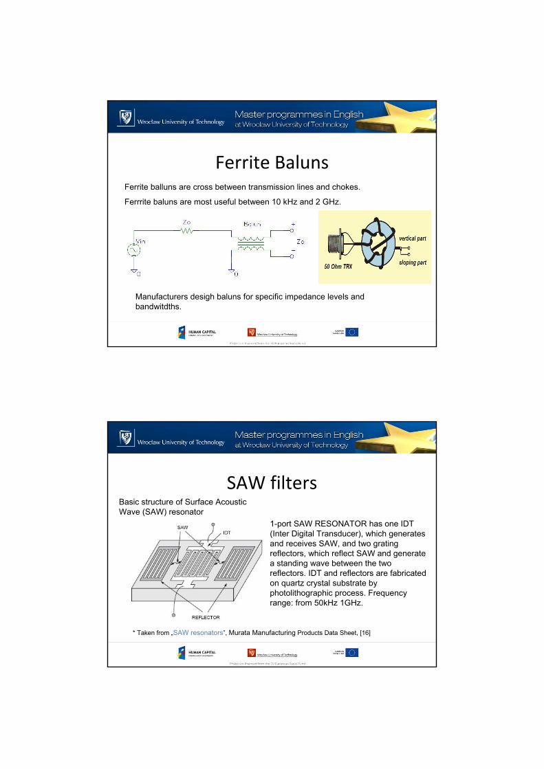
Ferrite BalunsFerrite balluns are cross between transmission lines and chokes.
Ferrrite baluns are most useful between 10 kHz and 2 GHz.
Manufacturers desigh baluns for specific impedance levels and
bandwitdths.
SAW filtersBasic structure of Surface Acoustic
Wave (SAW) resonator
* Taken from „SAW resonators”, Murata Manufacturing Products Data Sheet, [16]
1-port SAW RESONATOR has one IDT
(Inter Digital Transducer), which generates
and receives SAW, and two grating
reflectors, which reflect SAW and generate
a standing wave between the two
reflectors. IDT and reflectors are fabricated
on quartz crystal substrate by
photolithographic process. Frequency
range: from 50kHz 1GHz.
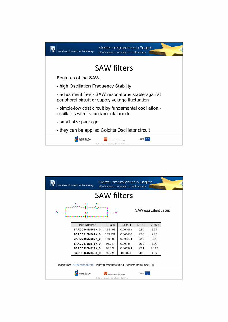
SAW filtersFeatures of the SAW:
- high Oscillation Frequency Stability
- adjustment free - SAW resonator is stable against
peripheral circuit or supply voltage fluctuation
- simple/low cost circuit by fundamental oscillation -
oscillates with its fundamental mode
- small size package
- they can be applied Colpitts Oscillator circuit
SAW filters
SAW equivalent circuit
* Taken from „SAW resonators”, Murata Manufacturing Products Data Sheet, [16]
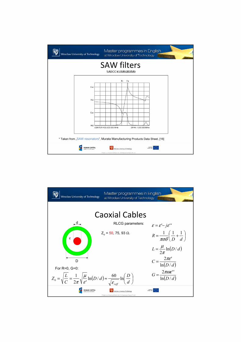
SAW filters
* Taken from „SAW resonators”, Murata Manufacturing Products Data Sheet, [16]
Caoxial Cablesd
D
ε
RLCG parameters:
( )
( )
( )dDG
dDC
dDL
dDR
j
/ln
''2
/ln
'2
/ln2
111
'''
πωε
πε
π
µ
πσδ
εεε
=
=
=
+=
−=
( )
≈==
d
DdD
C
LZ
reff
ln60
/ln'2
10
εε
µ
π
For R=0, G=0:
Zo = 50, 75, 93 Ω.
Caoxial Cables
Cut-off frequency:
dDf
reff
offcut+
=−
151.7
ε
Velocity of propagation:
reff
p
cv
ε=
Maximum peak power:( )
( )2
2
2
max/
/ln
480
max
dD
dDD
EP =
Caoxial Cables
* Taken from „Introduction to high-speed PCB design”, Kung [11]
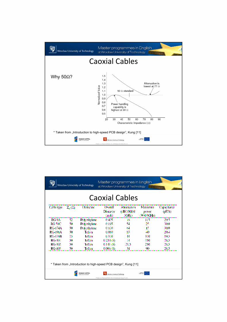
Caoxial Cables
Why 50Ω?
* Taken from „Introduction to high-speed PCB design”, Kung [11]
Caoxial Cables
* Taken from „Introduction to high-speed PCB design”, Kung [11]
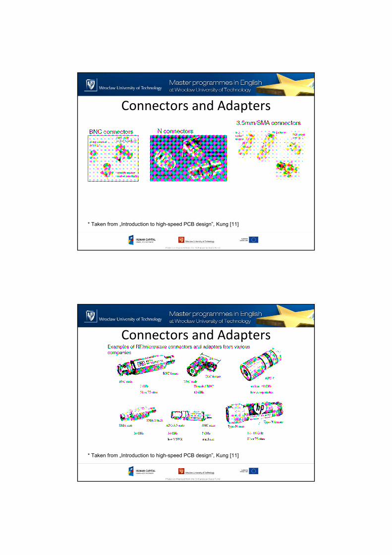
Connectors and Adapters
* Taken from „Introduction to high-speed PCB design”, Kung [11]
Connectors and Adapters
* Taken from „Introduction to high-speed PCB design”, Kung [11]
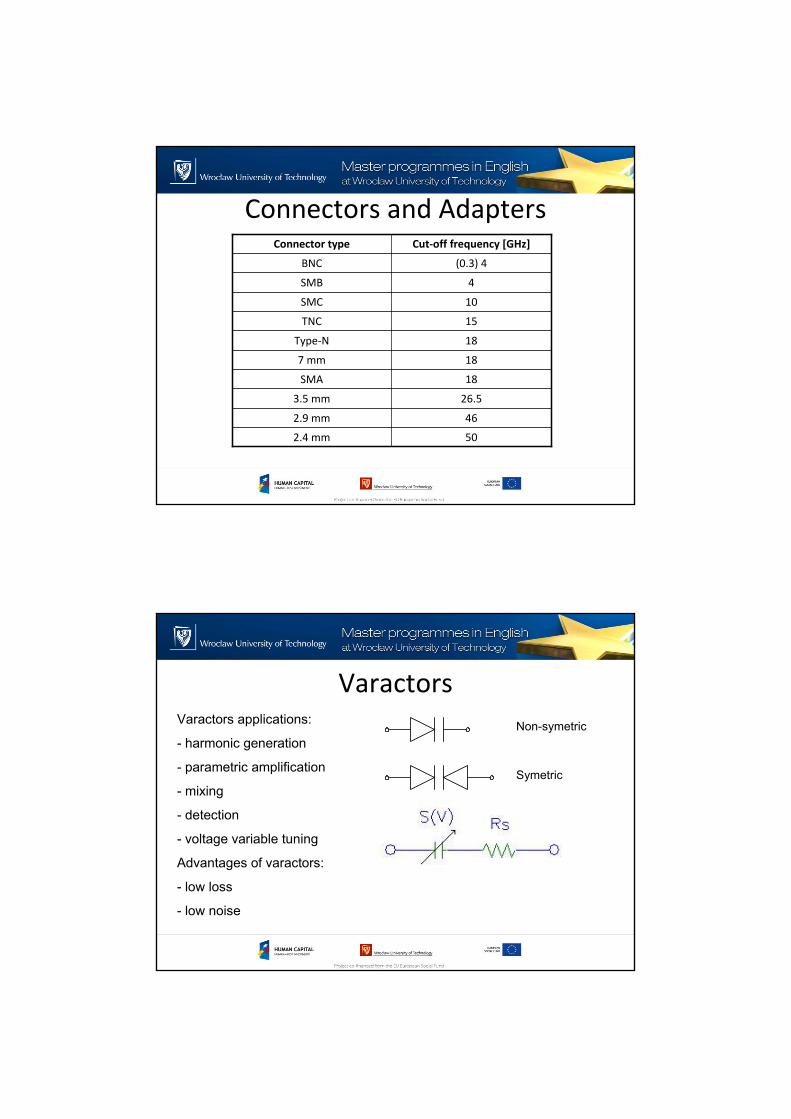
Connectors and Adapters
502.4 mm
462.9 mm
26.53.5 mm
18SMA
187 mm
18Type-N
15TNC
10SMC
4SMB
(0.3) 4BNC
Cut-off frequency [GHz]Connector type
VaractorsVaractors applications:
- harmonic generation
- parametric amplification
- mixing
- detection
- voltage variable tuning
Advantages of varactors:
- low loss
- low noise
Non-symetric
Symetric
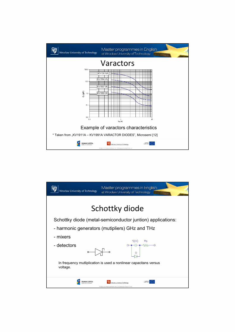
Varactors
Example of varactors characteristics
* Taken from „KV1911A – KV1991A VARACTOR DIODES”, Microsemi [12]
Schottky diode
Schottky diode (metal-semiconductor juntion) applications:
- harmonic generators (mutipliers) GHz and THz
- mixers
- detectors
In frequency mutliplication is used a nonlinear capacitans versus
voltage.
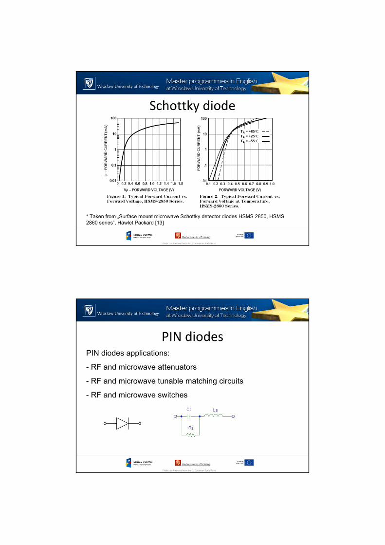
Schottky diode
* Taken from „Surface mount microwave Schottky detector diodes HSMS 2850, HSMS
2860 series”, Hawlet Packard [13]
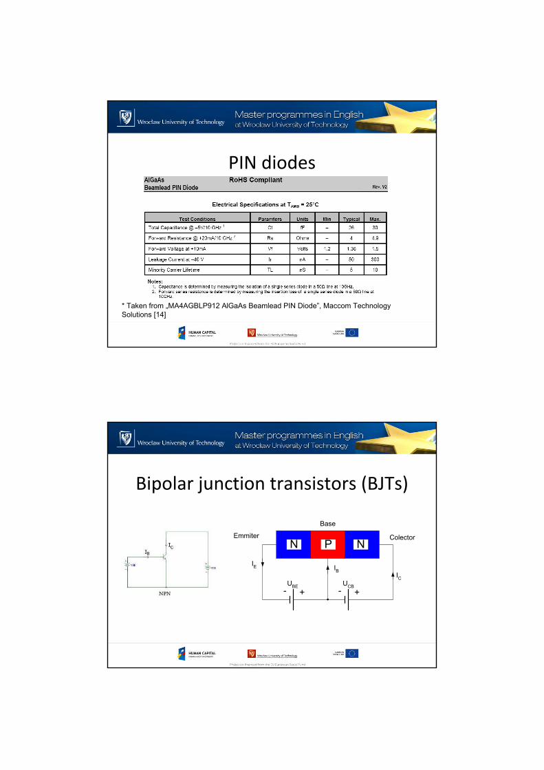
PIN diodesPIN diodes applications:
- RF and microwave attenuators
- RF and microwave tunable matching circuits
- RF and microwave switches
PIN diodes
* Taken from „MA4AGBLP912 AlGaAs Beamlead PIN Diode”, Maccom Technology
Solutions [14]
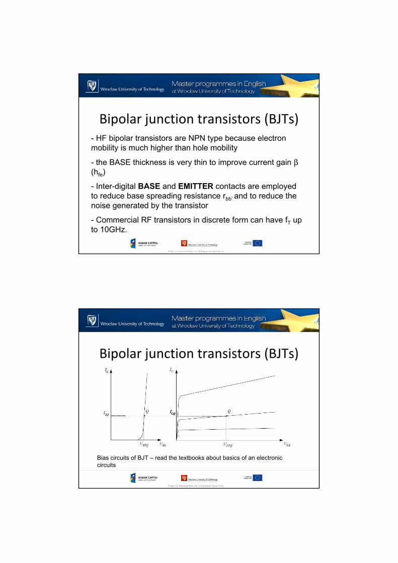
Bipolar junction transistors (BJTs)
P N
IC
N
- +UCB
- +UBE
ColectorEmmiter
Base
IE I
B
Bipolar junction transistors (BJTs)
- HF bipolar transistors are NPN type because electron
mobility is much higher than hole mobility
- the BASE thickness is very thin to improve current gain β(hfe)
- Inter-digital BASE and EMITTER contacts are employed
to reduce base spreading resistance rbb’ and to reduce the
noise generated by the transistor
- Commercial RF transistors in discrete form can have fT up
to 10GHz.
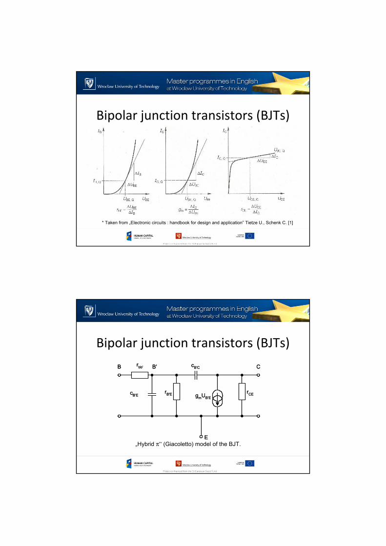
Bipolar junction transistors (BJTs)
Bias circuits of BJT – read the textbooks about basics of an electronic
circuits
Bipolar junction transistors (BJTs)
* Taken from „Electronic circuits : handbook for design and application” Tietze U., Schenk C. [1]
Bipolar junction transistors (BJTs)
B C
E
rCE
rB'E
B'rbb'
cB'E
cB'C
gmUB'E
B C
E
rCE
rB'E
B'rbb'
cB'E
cB'C
gmUB'E
„Hybrid π” (Giacoletto) model of the BJT.
Bipolar junction transistors (BJTs)
T
CQ
EB
Ir
ϕ
β='
T
CQ
m
Ig
ϕ=
CQ
EYCE
I
Ur =
m
DC
CBCBCB
U
Ucc
−
−= 10''
T
m
TT
CQ
EB
g
f
Ic
ωϕπ==
2'
Hybrid π model elements.
For frequencies above 300 MHz transistor
should be modelled by ‘S’ parameters.
Bipolar junction transistors (BJTs)
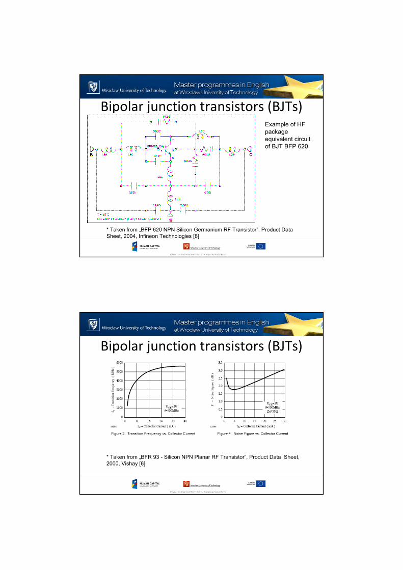
Bipolar junction transistors (BJTs)
* Taken from „BFP 620 NPN Silicon Germanium RF Transistor”, Product Data
Sheet, 2004, Infineon Technologies [8]
Example of HF
package
equivalent circuit
of BJT BFP 620
Bipolar junction transistors (BJTs)
* Taken from „BFR 93 - Silicon NPN Planar RF Transistor”, Product Data Sheet,
2000, Vishay [6]
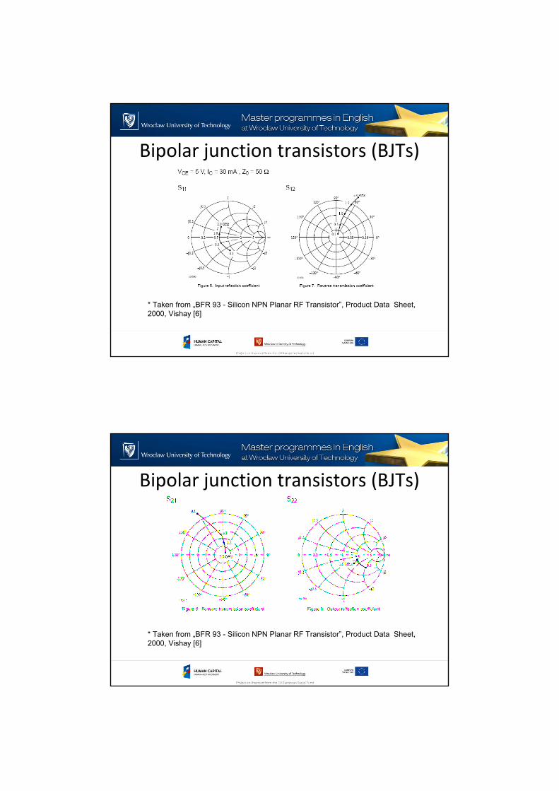
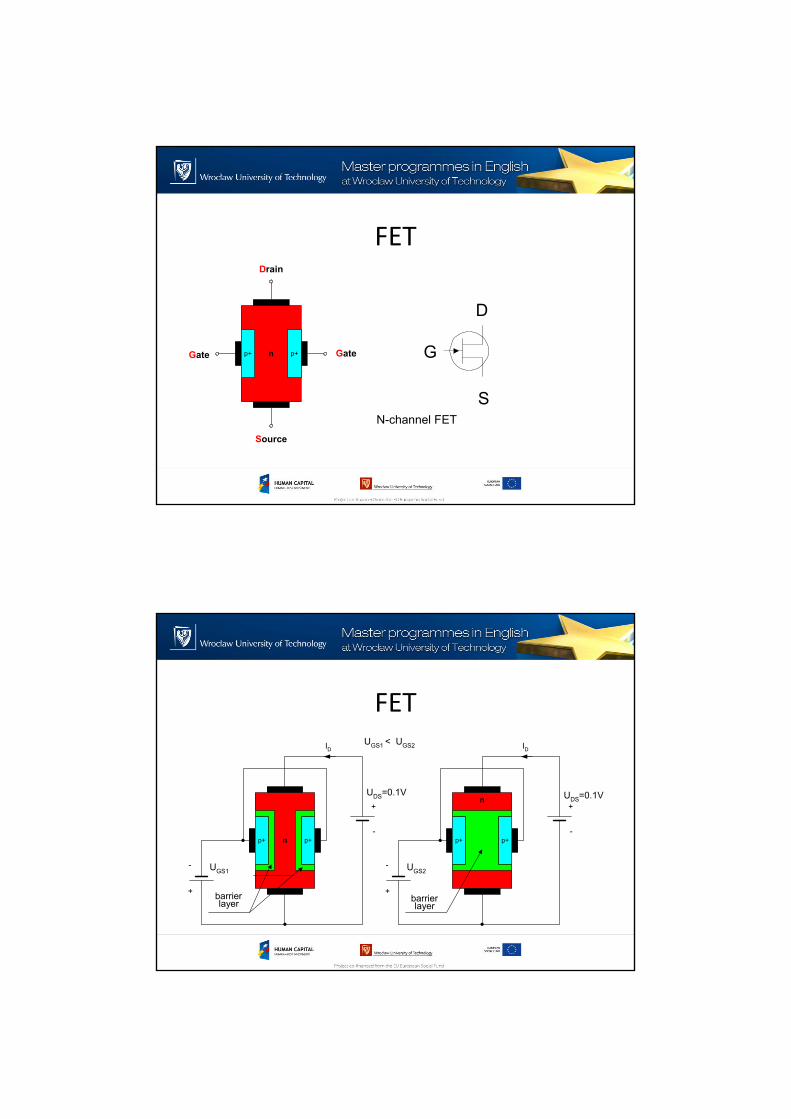
Bipolar junction transistors (BJTs)
* Taken from „BFR 93 - Silicon NPN Planar RF Transistor”, Product Data Sheet,
2000, Vishay [6]
Bipolar junction transistors (BJTs)
* Taken from „BFR 93 - Silicon NPN Planar RF Transistor”, Product Data Sheet,
2000, Vishay [6]
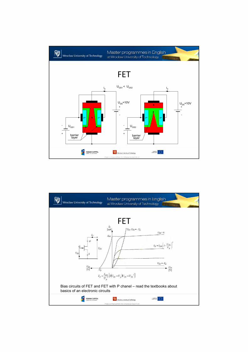
FET
n p+p+
Drain
Source
Gate Gate
D
G
SN-channel FET
FET
n p+p+
+
-
UGS1
+
-
UDS=0.1V
p+p+
+
-
UGS2
+
-
UDS=0.1V
n
UGS1
< UGS2I
DID
barrierlayer
barrierlayer
FET
n p+p+
+
-
UGS1
+
-
UDS=10V
p+p+
+
-
UGS2
+
-
UDS=10V
n
UGS1
< UGS2I
DID
barrierlayer
barrierlayer
FET
Bias circuits of FET and FET with P chanel – read the textbooks about
basics of an electronic circuits
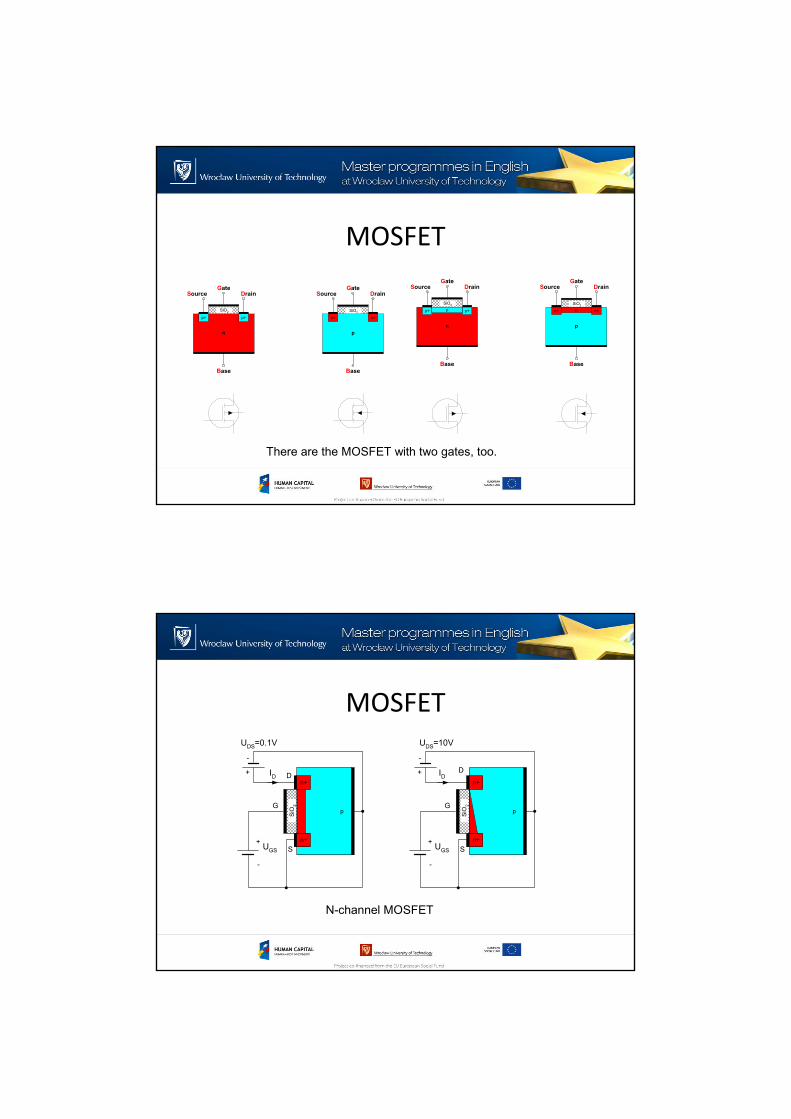
MOSFET
n
p+
DrainSource
Base
Gate
p+
SiO2
p
n+
DrainSource
Base
Gate
n+
SiO2
p p
p
n+
DrainSource
Base
Gate
n+
SiO2
n
p+
DrainSource
Base
Gate
p+
SiO2
There are the MOSFET with two gates, too.
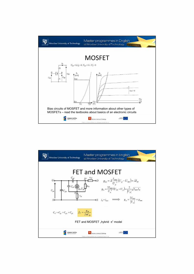
MOSFET
UGS
D
G
S+
-
UGS
D
G
S
ID
ID
UDS=0.1V U
DS=10V
n+
n+
SiO
2
p
n+
n+
SiO
2
p
+
-
+
-
+
-
N-channel MOSFET
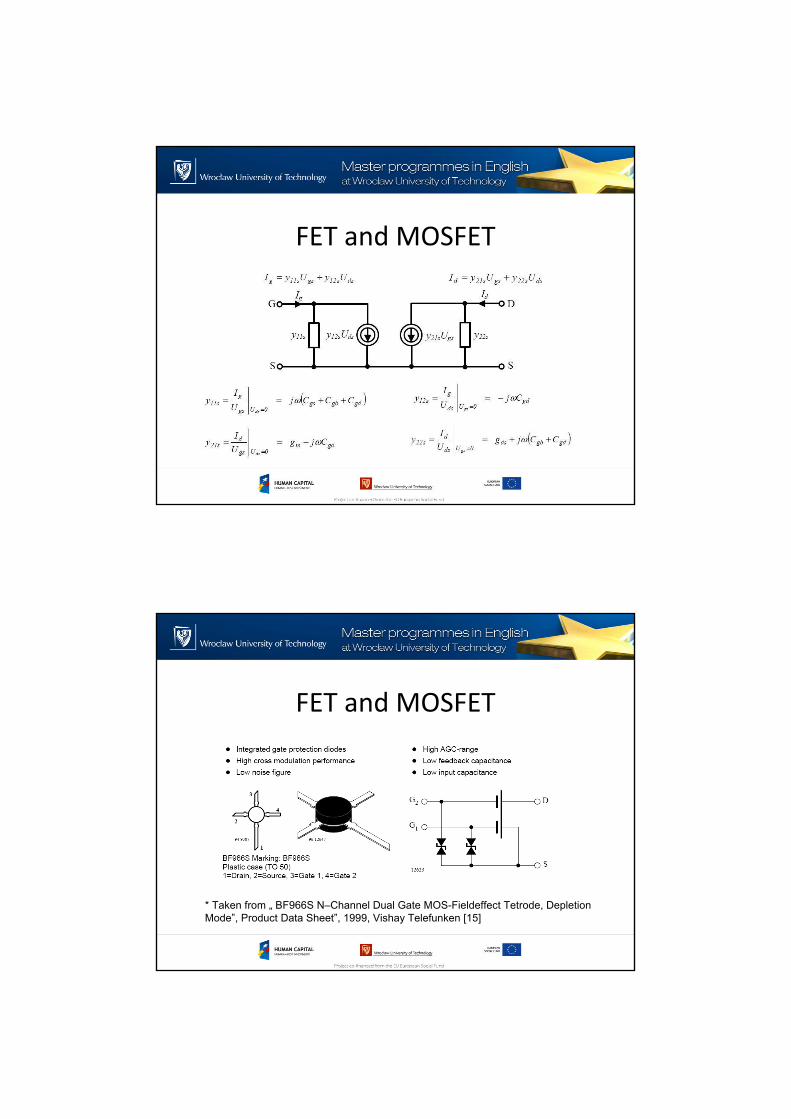
MOSFET
Bias circuits of MOSFET and more information about other types of
MOSFETs – read the textbooks about basics of an electronic circuits
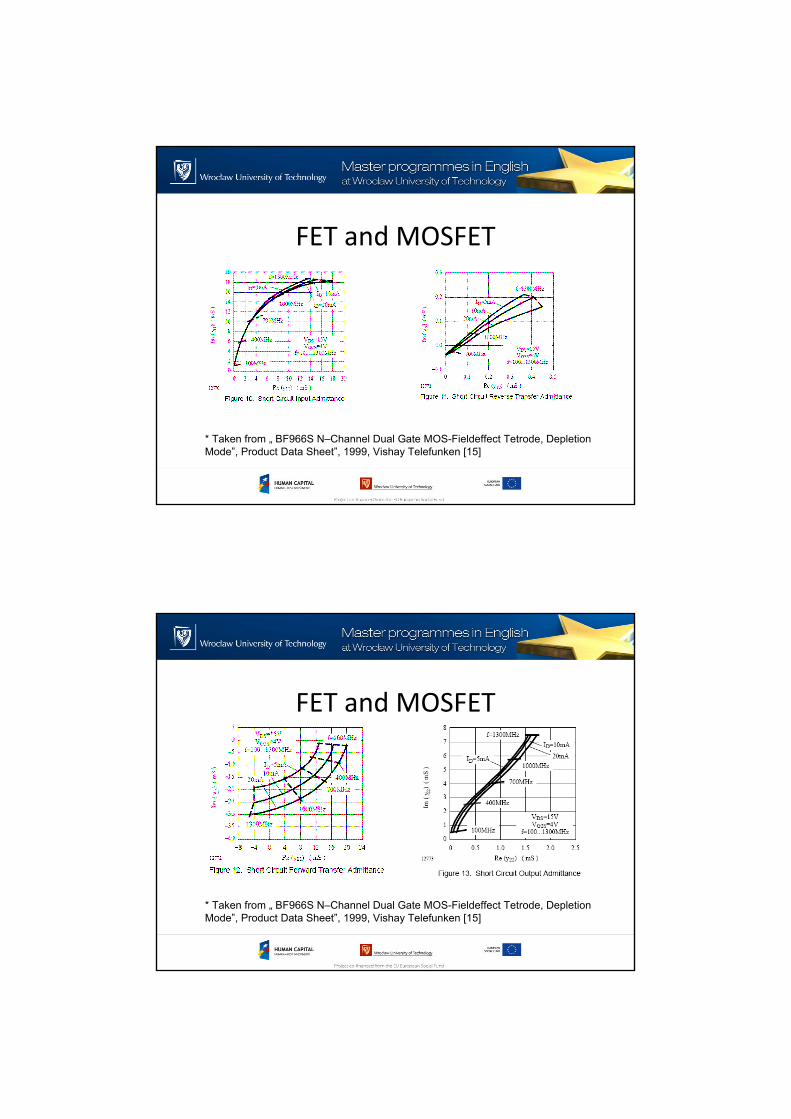
FET and MOSFET
FET and MOSFET „hybrid π” model
FET and MOSFET
FET and MOSFET
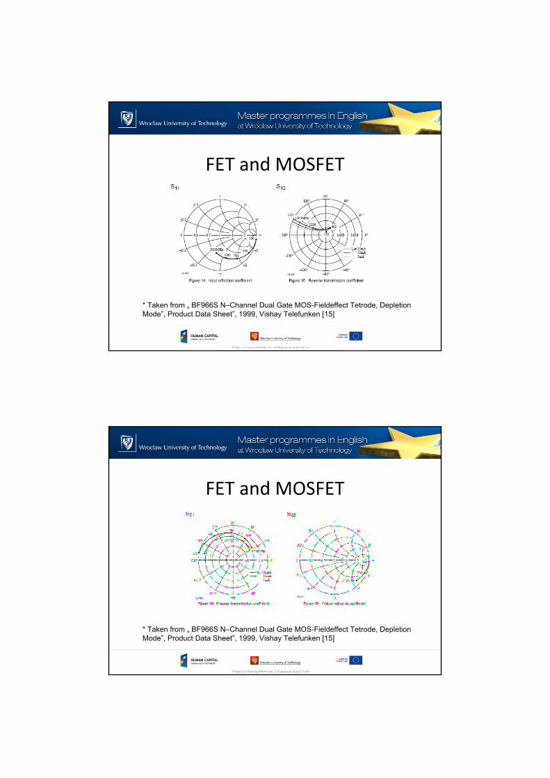
* Taken from „ BF966S N–Channel Dual Gate MOS-Fieldeffect Tetrode, Depletion
Mode”, Product Data Sheet”, 1999, Vishay Telefunken [15]
FET and MOSFET
* Taken from „ BF966S N–Channel Dual Gate MOS-Fieldeffect Tetrode, Depletion
Mode”, Product Data Sheet”, 1999, Vishay Telefunken [15]
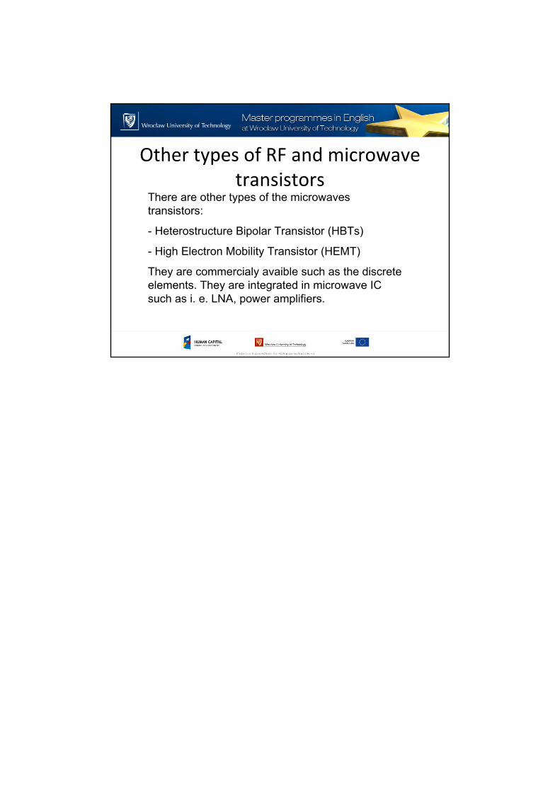
FET and MOSFET
* Taken from „ BF966S N–Channel Dual Gate MOS-Fieldeffect Tetrode, Depletion
Mode”, Product Data Sheet”, 1999, Vishay Telefunken [15]
FET and MOSFET
* Taken from „ BF966S N–Channel Dual Gate MOS-Fieldeffect Tetrode, Depletion
Mode”, Product Data Sheet”, 1999, Vishay Telefunken [15]
FET and MOSFET
* Taken from „ BF966S N–Channel Dual Gate MOS-Fieldeffect Tetrode, Depletion
Mode”, Product Data Sheet”, 1999, Vishay Telefunken [15]
Other types of RF and microwave
transistorsThere are other types of the microwaves
transistors:
- Heterostructure Bipolar Transistor (HBTs)
- High Electron Mobility Transistor (HEMT)
They are commercialy avaible such as the discrete
elements. They are integrated in microwave IC
such as i. e. LNA, power amplifiers.