Geoff Varrall Page 1 09/05/2007 RF Cost Economics for Handsets STUDY A study for the GSMA on the RF cost and performance implications for handsets supporting non standard band allocations. Researched and written by RTT with market data from The Mobile World. This Study provides the basis for the RF Cost Economics for Handsets White Paper prepared for the GSM Association. The White Paper is available as a download www.rttonline.com/research/RFCostEconomicsForHandsets-whitepaper.pdf May 2007 LEGAL NOTICE Neither the GSM Association nor their Members or Associate Members are responsible for the use that might be made of this publication. The views expressed in this publication are the sole responsibility of the author(s) and do not necessarily reflect the views of the GSM Association, their Members or Associate Members.
Transcript
Geoff Varrall Page 1 09/05/2007
RF Cost Economics for Handsets STUDY A study for the GSMA on the RF cost and performance implications for handsets supporting non standard band allocations. Researched and written by RTT with market data from The Mobile World. This Study provides the basis for the RF Cost Economics for Handsets White Paper prepared for the GSM Association. The White Paper is available as a download www.rttonline.com/research/RFCostEconomicsForHandsets-whitepaper.pdf May 2007 LEGAL NOTICE Neither the GSM Association nor their Members or Associate Members are responsible for the use that might be made of this publication. The views expressed in this publication are the sole responsibility of the author(s) and do not necessarily reflect the views of the GSM Association, their Members or Associate Members.
Index Section Title Page CHAPTER 1 INTRODUCTION 1 RF Cost Economics for handsets (context) 4 2 Assumptions used – summary of findings 5 3 Overall purpose of the study 6 4 Target readership 7 5 Sources and confidentiality of data 7 6 Possible impact of new technologies and issues of
technology maturity and availability 7
7 Component functions in a cellular phone 9 Figure 1 Block diagram (Analog Devices) 9 8 Present frequency band allocations and their impact on RF
devices and RF design 9
Table 1 Band allocations and duplex spacing 10 9 The RF BOM compared to other components 11 Figure 2 Pie chart of RF BOM as a percentage of other
components 11
10 The single band to multi band transition 12 Table 2 Present and possible future allocations by
technology 14
11 Other practical design considerations- band to band intermodulation within the handset
15
12 The need to support higher frequencies 15 Table 3 Linearity requirements by technology 16 13 Co existence of wide area cellular transceivers with other RF
devices within the handset 18
CHAPTER 2 RF COMPONENT COST AND PERFORMANCE METRICS 18 1 The Tx/Rx switch for GSM 19 2 Band switching 19 3 Mode switching 19 4 The impact of increased RF integration on volume thresholds 20 5 Differentiating quantitative and qualitative factors 21 6 Quantifying the performance cost of non standard spectral
deployment 22
7 Differentiating RF technology and RF engineering costs 22 8 The impact of volume thresholds and maturity performance
thresholds on RF performance - a GSM example. 23
9 The impact of volume thresholds and maturity performance thresholds on RF performance - a UMTS example.
24
Figure 3 Sensitivity measurements on four UMTS phones 25 Figure 4 Relationship of RF yield to the RF BOM 26 10 The RF functions in a phone 26 11 RF Device functionality, useful inventions over the past 100 27
Geoff Varrall Page 3 09/05/2007
years 12 Present day issues of RF Device integration 28 13 Antennas for candy bar handsets 28 Figure 5 Antenna bandwidth plotted against chassis length 29 14 Two part clamshell handset antennas and slider phone
antennas 29
Figure 6 Equivalent circuit, showing the effect of the flexi circuit and the inter component capacitance.
29
Figure 7 Clamshell handset example 30 15 The antenna Tx/Rx switch module for GSM, duplexer for
UMTS 31
16 Other front end switch paths 32 17 Filtering using SAW and BAW filters 34 18 MEMS resonators 34 19 MEMS duplexers 34 20 Implications for future radio systems 34 21 Present Handset status 35 Table 4 RF BOM of a tri band GSM handset in 2003 35 22 Present RF BOM cost optimisation for ULCH(ultra low cost)
handsets 37
Figure 8 GSM Quad band transceiver block diagram (Silabs) 37 23 Lower cost oscillators 38 24 Production test times and costs 39 25 Additional nuisance costs 39 26 Additional BOM implications for GSM/dual mode handsets 40 27 An example from the 1.7GHz band in Japan 41 Figure 9 SAW diplexer and duplexer examples (Murata) 41 28 Antenna Costs 41 29 Cost and Performance metrics 42 Table 5 Comparison of PA process technologies 43 30 Dual band versus tri band versus quad band price
differentials 44
31 GSM versus UMTS cost cross over points 46 Table 6 Simplified RF channel spacing by generation 46 Table 7 UMTS, WiMax and UTRAN/LTE channel spacing 46 CHAPTER 3 NON RECURRING ENGINEERING COSTS 48 1 Non recurring costs and their impact on RF BOM costs for
limited volume markets 48
2 Quantifying NRE costs 49 Table 8 NRE cost and the industry value chain 49 3 Defining and differentiating tier 1, tier 2 and tier 3 vendors 50 4 Silicon/component vendor NRE including type approval
testing 51
5 Handset Manufacturer NRE including conformance testing 52 6 An extreme example of the cost/volume/vendor
choice/pricing effect. 54
7 Network operator NRE and the ‘Portfolio effect’ 55 8 Opportunity cost thresholds for silicon vendors and their 56
Geoff Varrall Page 4 09/05/2007
supporting component vendors – the ‘activation energy’ effect
9 The impact of industry growth rates on NRE ROI policy 57 10 The impact of industry and GDP growth rates on component
costs 58
11 The end user 58 CHAPTER 4 SUMMARY 1 Summary- Recurring Costs 59 2 Exceptions that may add to the cost premium for additional
bands 59
3 Summary - non recurring costs 59 CHAPTER 5 RF ECONOMIES OF SCALE, COST CURVES AND
THRESHOLDS 60
1 Summary- scale economies 60 2 The size of the global handset market 61 Graph 1 GSM Quad band market 61 Graph 2 relative market values by technology 62 Graph 3 Global mobile market by technology 62 Graph 4 Cumulative GSM subscriber base, 1991-1997 63 Graph 5 Global mobile customers by technology, December
1997 63
Graph 6 Global mobile customers by technology, June 2006 64 Graph 7 W CDMA subscribers 2002-2007 65 Graph 8 WCDMA handset sales 65 Graph 9 Index of adoption rate, one year after launch 66 Graph 10 GSM handset BOM 67 Graph 11 BOM for multi band W CDMA handsets 68 Graph 12 Additional costs amortised over typical handset
volumes in eight countries 69
Table 9 Premium ($) to amortise opportunity cost and non-standard components at varying volumes
70
CHAPTER 6 BACKGROUND NOTES ON TECHNOLOGY 1 Frequency and time division duplexing 71 2 Frequency stability in OFDM systems 72 3 ADC linearity 72 4 Foundries 72 5 Integration levels and lower cost printed circuit boards 74 6 Integration levels- enabling self test and calibration on the
production line 74
7 RF MEMS and tuneable RFIC’s (software defined radios) 74 8 RF efficiency metrics 75 9 Production efficiency metrics 76 10 The impact of DVB H and T DMB and other receiver functions 76 11 Conformance testing 76 Figure 10 Number of hours needed to conformance test a
ULCH (ultra low cost) handset 77
Geoff Varrall Page 5 09/05/2007
Figure 11 ULCH 2 G handset testing 77 Figure 12 ULCH BOM analysis 78 Figure 13 3G test time 78 Figure 14 Single band 3G ULCH handset 78 Figure 15 Single band plus dual band GSM 79 Figure 16 3G Americas ULCH specification 80 Figure 17 US ULCH test costs 80 12 Matching 81 13 RF BOM – Relationship to GSM and WCDMA wholesale
handset price points 82
14 UMTS Spectrum Design Dissipation 83 15 Learning curve effects, cost and ARP reductions and the
impact on vendor margins 86
16 Global handset sales and the impact of varying year on year volume growth in the industry.
87
CHAPTER 7 REFERENCES,SOURCES AND THANKS 1 References 88 2 Additional information sources 90 Acknowledgements and thanks Special thanks are due to the The Mobile World for their work on market statistics for this study and to Herschel Shosteck for reviewing of early drafts of the document, also to the numerous other reviewers who have helped resolve differences in industry opinion on costs and technology trends. CHAPTER 1 INTRODUCTION 1) RF Cost Economics for handsets -context This document studies the RF cost and performance implications for handsets supporting non standard band allocations and determines the RF economies of scale needed to achieve an adequate supply of cost competitive and performance competitive handsets. It is the supporting document for the White Paper, ‘RF Cost Economics for Handsets’ that can be downloaded from http://www.rttonline.com/rfcosteconomics/handsets/whitepaper The study includes cost curves for the RF components for cellular handsets deployed into non-standard spectral allocations. These allocations are, typically, country or region specific. The costs are based on present non recurring engineering (NRE) return on investment (ROI) policies generally adopted in the industry. Costs are assessed across the industry value chain in a ‘foundry to phone’ analysis of the risk factors implicit in bringing RF based products to market
2) Assumptions used in the study and a summary of findings The study is based on the assumption that there is an underlying and ongoing need to lower costs and provide a continuously improving user experience in terms of data rates and duty cycles and a parallel need to support multiple simultaneous data streams. Cost reduction implies a steady increase in the level of integration used in cellular phones. However RF functions have been traditionally difficult to integrate. For example, the higher power levels used in wide area cellular systems make it problematic to place devices such as RF power amplifiers in close proximity to other RF and non-RF functions. In terms of spectral policy making, it is assumed that future cellular phones will become increasingly frequency transparent, able to access multiple frequencies across multiple bands. However, as we shall discover in this study, this requirement is at odds with the parallel need to increase integration levels to achieve ever lower component and production cost targets. As integration levels increase, the number of RF components reduces, the RF bill of materials (RF BOM) goes down and production costs go down. However moving to a higher level of integration implies an increase in non-recurring engineering costs. An increase in non-recurring RF engineering and design costs implies that higher market volumes are needed to achieve RF economies of scale. NRE costs can be reduced by adopting lower levels of device integration but the RF BOM will increase and the form factor of the phone will increase. RF performance may or may not decrease but will be more variable from phone to phone (handset to handset, batch to batch variations from the production line). 3) Overall purpose of the study ‘RF Cost Economics for Handsets’ sets out to establish the specific market volumes needed to achieve an adequate supply of cost economic performance competitive handsets and suggests that these required market volumes are increasing rather than decreasing over time. Specifically we quantify the fiscal impact of non standard spectral allocations in terms of unrecoverable RF NRE costs and incremental increases in the RF
Geoff Varrall Page 7 09/05/2007
BOM and show how these costs invalidate otherwise justifiable spectral and network investment business models. This first chapter, Chapter 1 establishes the context of the study, Chapter 2 analyses RF component cost and RF performance metrics, (recurring/variable costs), Chapter 3 quantifies non recurring/fixed RF engineering costs, Chapter 4 summarises the scale economies needed to deliver cost competitive performance competitive product to market, Chapter 5 relates these scale economy thresholds to present market metrics, Chapter 6 provides background information on a range of RF related technology issues, Chapter 7 lists references used throughout the study.
4) Target readership The study contains substantial technology and engineering detail but is relevant and accessible to a readership with a generalist interest and/or non-technical background.
It is intended to be directly useful for economists presently modeling handset costs and service pricing in developed and emerging markets, for terminal management team leaders within the operator community, spectral and standards and IPR policy makers and investors wishing to qualify and quantify present and future spectral and network value.
5) Sources and confidentiality of data included in this report We are indebted to the wide cross section of colleagues from within the industry who have contributed to this study with comments and/or cost based data.
To maintain confidentiality, these sources are referenced in terms of date that information has been supplied to us by phone and/or e-mail but are not necessarily directly identified.
We do however identify publicly available tabular data supplied by specific vendors and related reference documentation.
6) Possible impact of new technologies and issues of technology maturity and availability Although handsets are becoming more integrated over time, the practical implementation of a single chip software definable phone remains elusive. It is relatively easy to count at least 100 separate components in a phone including modules that themselves contain multiple functions on separate parts of a common substrate. About 75% of these components in present cellular phones are passive, inductors, capacitors and filters. These devices are frequency specific.
Geoff Varrall Page 8 09/05/2007
Supporting additional frequencies in a handset implies an increase in the number of passive components. This implies higher material and manufacturing costs. (Reference 1, See References section, Chapter 7, at the end of this document). Active devices such as the power amplifier can be designed to cover relatively wide frequency bands but become harder to match and lose overall efficiency. Non standard frequency allocations therefore have an impact on passive and active device requirements. New MEMS (micro electrical mechanical system) based technologies offer the potential opportunity to integrate many of these functions on to an RFIC, including for example, switch and tuneable filter functions. Additional background on MEMS devices and tuneable RFIC’s is available in Chapter 6, Section 7 of the Background Notes. The Background Notes section is immediately prior to the References section at the end of this document. Tuneable structures integrated with other active components can be used to implement wideband power amplifiers, broadband tuneable matching networks and adaptive antenna matching. Similarly MEMS devices may be used to vary the load impedance of power amplifiers so that they will work efficiently at varying power levels over a relatively wide range of frequencies. MEMS also potentially address the problem of duplexing, particularly in UMTS phones. In GSM, duplexing, (the separation of transmit and receive channels within a specific frequency band) can be achieved with a front-end switch as the phones are not transmitting and receiving at the same time. In UMTS, transmission takes place at the same time as reception. Adding a band means another duplex filter needs to be added which has an associated direct cost and an associated indirect cost (takes up additional board space and needs matching components). There are presently proposals for MEMS based active digitally tuneable duplexers, also known as digital duplexers, which will potentially resolve these band specific UMTS specific duplex cost overheads. (Reference 2) These techniques together will enable a transition towards single chip software defined radios that will help eliminate many present spectrally specific device and design issues.
Geoff Varrall Page 9 09/05/2007
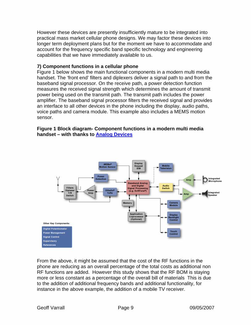
However these devices are presently insufficiently mature to be integrated into practical mass market cellular phone designs. We may factor these devices into longer term deployment plans but for the moment we have to accommodate and account for the frequency specific band specific technology and engineering capabilities that we have immediately available to us. 7) Component functions in a cellular phone Figure 1 below shows the main functional components in a modern multi media handset. The ‘front end’ filters and diplexers deliver a signal path to and from the baseband signal processor. On the receive path, a power detection function measures the received signal strength which determines the amount of transmit power being used on the transmit path. The transmit path includes the power amplifier. The baseband signal processor filters the received signal and provides an interface to all other devices in the phone including the display, audio paths, voice paths and camera module. This example also includes a MEMS motion sensor. Figure 1 Block diagram- Component functions in a modern multi media handset – with thanks to Analog Devices
From the above, it might be assumed that the cost of the RF functions in the phone are reducing as an overall percentage of the total costs as additional non RF functions are added. However this study shows that the RF BOM is staying more or less constant as a percentage of the overall bill of materials This is due to the addition of additional frequency bands and additional functionality, for instance in the above example, the addition of a mobile TV receiver.
8) Present frequency band allocations and their impact on RF devices and design. There are presently nine RF duplex spaced frequency bands between 800 MHz and 2.6 GHz specified by 3GPP (the 3G Partnership Project) which are either presently used by GSM or UMTS and/or are suitable for longer term UMTS implementation. The nine bands are as follows: Table 1 Band allocations and duplex spacing Band 3GPP Allocation Uplink Duplex spacing Downlink Region I 2100 2x60 MHz 1920-1980 190 MHz 2110-2170 Present UMTS II 1900 2x60 MHz 1850-1910 80 MHz 1930-1990 US PCS III 1800 2x75 MHz 1710-1785 95 MHz 1805-1880 GSM Europe, Asia, Brazil IV 1700/2100 2x45 MHz 1710-1755 400 MHz 2110-2155 New US V 850 2x25 MHz 824-849 45 MHz 869-894 US and Asia VI 800 2X10 MHz 830-840 45 MHz 875-885 Japan VII 2600 2x70 MHz 2500-2570 120 MHz 2620-2690 New VIII 900 2X35 MHz 880-915 45 MHz 925-960 Europe and Asia IX 1700 2x35 MHz 1750-1785 95 MHz 1845-1880 Japan Each of these bands are subdivided into transmit bands and receive bands. The duplex separation varies between 45 MHz (800/850/900 MHz bands) and 400 MHz (Band IV US AWS). The lower band is always mobile transmit as the propagation conditions are more favourable. This duplex separation is one of the main mechanisms for delivering good sensitivity (range and/or data throughput) from cellular phones. The UMTS band also includes non duplexed channel allocations which can be used (though at time of writing have not been implemented) for time division duplexed UMTS. (See Note 1 in Chapter 6, the Technology Background section at the end of this report for additional information on the spectral and technology implications of time division duplexing and Note 14 on the impact that UMTS spectral allocation has on NRE costs). The choice of frequency, the guard bands between band allocations and the duplex separation of the uplink and downlink within each individual band all have a profound influence on the architecture of the phone and the active and passive devices used in the phone. Additionally, legacy spectral allocations may need to be supported in some handset frequency plans and future re-purposed UHF TV allocations between 470 and 862 MHz may also need to be accommodated.
Geoff Varrall Page 11 09/05/2007
These ‘wide area’ cellular radio transceiver functions may also need to physically co exist with local area (WiFi) and personal area transceivers and with (easily desensitised) receive only functions such as GPS or DVB TV. Digital filtering techniques and architectural innovations, for example direct conversion receivers, translational (GSM) and polar loop (EDGE and WCDMA) transmit architectures, have been developed that minimise the present RF component count and RF component cost implications of multi band and multi mode handsets. As a result, it would be reasonable to assume that RF component costs represent a declining percentage of the BOM of a modern cellular handset. However, this study concludes that, despite these technical advances, RF costs have remained relatively stable as a percentage of the total BOM over time and are likely to remain so. This is due to an increase in RF performance expectations and user expectations of handset functionality, including data rates, terminal form factor and battery life (user duty cycle). 9) The RF BOM compared to other components The pie chart (Figure 2) gives an indication of the typical value split between functions, in this case in an Ultra Low Cost Handset. Figure 2 the RF BOM compared to other components
Handset BOM
LCD9%
Charger4%
Keypad9%
Battery4%
PCB13% Memory
9%
Mechanical9%
Baseband28%
RF7%
Earpiece4% Packaging
4%
We have said that the RF BOM is staying relatively constant over time as a percentage (between 7 % and 10%) of the overall BOM of the phone and that this is true irrespective of whether the phone is an entry level, mid tier or high end device.
Geoff Varrall Page 12 09/05/2007
Not all respondents agree that this is necessarily the case. A mid tier camera phone for example had a value split of about 5% for the RF (including Bluetooth). The logic and digital circuits accounted for about 30%, memory at 12%, the LCD at 10%, the camera at 11%, PCB and electro mechanical components at 13%, mechanical components at 14% and ‘other bits’ at 6%. It could be argued of course that the imaging bandwidth of this device might deserve more highly specified RF functionality. It is however true that a need to support additional access technologies will introduce additional costs. These costs include non-recurring expenditure (NRE) and component cost. This study quantifies the volume thresholds that need to be achieved to support a supply of handsets that can be considered to be ‘cost economic’ in terms of RF related NRE and RF related component cost. This volume threshold is higher than presently acknowledged by many in the industry and is increasing over time. In addition, it can be hard to achieve competitive RF performance unless certain volume thresholds are achieved. This study quantifies the ‘performance volume thresholds’ and related ‘performance scaling effects’ which need to be factored in to spectral valuation and spectral allocation policy. In doing so we quantify the escalating cost and risk factors associated with geographically specific non-standard spectral allocations particularly in countries with relatively small addressable markets. Many of the cost and risk factors can also be applied to the implementation of non standard technologies into either standard or non standard spectrum. Thus some of the findings of the study are of direct relevance to operator study teams presently validating future air interface technology options. 10) The single band to multiband transition We use present single mode multi band GSM as a cost base, specifically taking dual band, tri band and quad band handsets as our starting point. Dual band GSM phones are designed to work at 900MHz (Band VIII) and 1800 MHz (Band III) for European and Asian markets, Tri band GSM add in the 1900 MHz (Band II) for the US and Latin America. Quad band GSM handsets add in the 850 MHz Band (Band V). The global market for quad band devices is 900 million units out of a total of one billion units. (See Chapter 5 Graph 1 RF Cost Economics, Cost Curves and Thresholds). This explains the present silicon vendor focus on quad band cost and performance optimisation. By default this means that these devices are
Geoff Varrall Page 13 09/05/2007
potentially the most cost and performance optimised products presently available though in practice most vendors ship dual band phones as the lowest cost products. Tri band and quad band GSM products are shipped at a (relatively small) cost premium. The relatively small RF component cost premiums that presently apply to tri band and quad band handsets are a function of market volume. Supporting additional bands over and above these standard bands incurs a substantially larger component cost premium, quantifiable additional non recurring expenditure and a quantifiable risk in terms of product choice, product form factor, functionality and time to market delay. This is also applicable to GSM/UMTS dual mode handsets. These typically combine quad band GSM (850/900/1800/1900) with UMTS at 1900/2100 MHz though increasingly, support for UMTS at 850 and 1900 MHz for the US market is included together with UMTS at 900 and 1800 MHz to support refarming of existing GSM spectrum. Any discussion of the economics of adding an additional frequency band to a handset therefore has to comprehend the technology or technologies used to access that band. The technology used (GSM and/or GSM/UMTS) influences the RF architecture of the phone, the RF component cost of the phone and the non recurring engineering cost of getting that phone to market. It is of course possible to produce UMTS only devices and such devices have been and are being developed and sold into some markets, for example Japan. To date these devices have been disadvantaged in terms of their global roaming capability, for example they could not be used in the US. Present deployment of UMTS in to the 850 MHz band and potential deployment into the 1700/2100 AWS band in the US and 900/1800 MHz bands in other countries will reduce this disadvantage. So at some stage it may become economically attractive to revert to single mode handsets with the single mode being UMTS rather than GSM. For the time being, operators need to plan on the basis of implementing either a GSM only network or a dual mode GSM/UMTS network that implies a need for dual mode handsets. There may also be a perceived market need to support additional air interfaces that may or may not be band specific so dual mode handsets may in practice be multi mode handsets. The assumption is that operators in developing markets may be predisposed to opt for GSM only networks in order to realise lowest possible network roll out and operational costs and lowest cost handset availability.
Geoff Varrall Page 14 09/05/2007
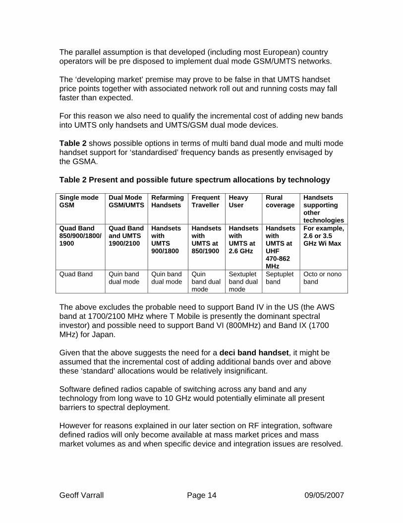
The parallel assumption is that developed (including most European) country operators will be pre disposed to implement dual mode GSM/UMTS networks. The ‘developing market’ premise may prove to be false in that UMTS handset price points together with associated network roll out and running costs may fall faster than expected. For this reason we also need to qualify the incremental cost of adding new bands into UMTS only handsets and UMTS/GSM dual mode devices. Table 2 shows possible options in terms of multi band dual mode and multi mode handset support for ‘standardised’ frequency bands as presently envisaged by the GSMA. Table 2 Present and possible future spectrum allocations by technology Single mode GSM
Dual Mode GSM/UMTS
Refarming Handsets
Frequent Traveller
Heavy User
Rural coverage
Handsets supporting other technologies
Quad Band 850/900/1800/ 1900
Quad Band and UMTS 1900/2100
Handsets with UMTS 900/1800
Handsets with UMTS at 850/1900
Handsets with UMTS at 2.6 GHz
Handsets with UMTS at UHF 470-862 MHz
For example, 2.6 or 3.5 GHz Wi Max
Quad Band Quin band dual mode
Quin band dual mode
Quin band dual mode
Sextuplet band dual mode
Septuplet band
Octo or nono band
The above excludes the probable need to support Band IV in the US (the AWS band at 1700/2100 MHz where T Mobile is presently the dominant spectral investor) and possible need to support Band VI (800MHz) and Band IX (1700 MHz) for Japan. Given that the above suggests the need for a deci band handset, it might be assumed that the incremental cost of adding additional bands over and above these ‘standard’ allocations would be relatively insignificant. Software defined radios capable of switching across any band and any technology from long wave to 10 GHz would potentially eliminate all present barriers to spectral deployment. However for reasons explained in our later section on RF integration, software defined radios will only become available at mass market prices and mass market volumes as and when specific device and integration issues are resolved.
Geoff Varrall Page 15 09/05/2007
In practice, at least for the next 5 to 7 years, each additional band whether ‘standard’ (as defined by 3GPP) or ‘non standard’ (a country specific allocation not included in the table above) will incur substantial non-recurring investment cost and (related) component cost multipliers. We will demonstrate that the market volumes needed to economically cost justify additional band support are substantial and are increasing over time. Sufficient market volumes are unlikely to be achieved in any countries or regions other than China, India, Europe and possibly the USA/ Latin America. Even in these ‘large local markets’ the entry costs and risks of non-standard bands are in practice far higher then presently acknowledged. 11) Other practical design considerations - band to band inter modulation within the handset Whenever two or more frequencies are mixed intentionally or unintentionally within a handset, they will produce sum and difference frequencies. This is known as inter modulation and can occur at receive frequencies and transmit frequencies or between transmit and receive frequencies. Frequencies are mixed or multiplied together intentionally within the frequency synthesiser to create new wanted frequencies to be modulated. The unwanted sum or difference frequency (the image) is filtered out. When frequencies mix together unintentionally, sum and difference products may translate unwanted signal energy into other bands within the phone or into other proximate devices. A new frequency band introduced into a handset will create a new set of inter modulation products that will need to be managed in terms of their potential impact on the other bands and radio systems used in the phone. Resolving these issues adds to the non recurring engineering cost, may result in time to market delay and may add to component cost if additional filtering or reciprocal mixing has to be introduced. 12) The need to support higher frequencies Table 2, shown earlier, comprehends the new extension/expansion band at 2.6 GHz and potential Wi Max bands at 3.5 GHz. Many handsets have Bluetooth transceivers and/or WiFi transceivers at 2.3 GHz (and possibly also WiFi at 5 GHz) but these are low power devices, generating not more than 10 milliwatts of transmit power. Wide area cellular systems require handsets to transmit at higher powers, typically 250 milliwatts, and to be able to reduce this output power in defined steps down to a few milliwatts (the dynamic output power range over which the phone has to operate).
Geoff Varrall Page 16 09/05/2007
Handset vendors have a choice of power amplifier technologies that are typically either based on CMOS (Complementary metal–oxide–semiconductor) or SiGe (Silicon Germanium) or GaAs (Gallium Arsenide) semiconductor processes. Simplifying a rather complex story, CMOS is lower cost and supports more aggressive integration but does not perform as well as GaAs particularly at higher frequencies. SiGe combines some of the advantages of CMOS and GaAs. GaAS also has some advantages in terms of delivering a better linearity/amplifier efficiency trade off, an important metric for UMTS and related technologies using a combination of phase and amplitude modulation. The requirement specifically is to deliver good linearity and efficiency at maximum power and good efficiency at minimum power. An optimum PA (power amplifier) technology choice for 3.5 GHz is unlikely to be the same as an optimum PA technology choice for 700 MHz. As a general rule, it gets harder to deliver gain without introducing excessive noise as frequency increases. An optimum PA technology choice for GSM is unlikely to be the same as an optimum PA technology choice for UMTS which requires more linearity to preserve the AM (amplitude modulation) characteristics in the modulated signal envelope. Table 3 Linearity requirements by technology Generation Technology Peak to
average ratio In dB
Power control dynamic range
1G AMPS 0 25 dB ETACS 0 25 dB JTACS 0 25 dB 2G GSM 0 30 dB PDC 3 - 5 30 dB TDMA/EDGE 3 - 5 35 dB 3G UMTS rel 99 5 80 dB UMTS rel 6/7 5 - 8 35 dB UTRAN/LTE and/or
or WiMax 8 – 17(TBD) TBD
Table 3 shows the overall trends over the past 20 years (first and second generation cellular) and likely trends over the next five to ten years in terms of the peak to average ratio of the modulated signal envelope (which determines the amount of linearity needed in the amplifier) and the power control dynamic range (which determines the upper and lower power outputs required from the device).
Geoff Varrall Page 17 09/05/2007
GSMK was chosen for GSM because the modulated signal envelope has no intentional amplitude modulation and could/can therefore use Class C amplifiers (as used in FM analogue systems) albeit with an increased dynamic range (lowest to highest output power). These power amplifiers could be/can be up to 55% efficient. All other evolving technology options including evolved variants of GSM (EDGE) have used/use a combination of phase and amplitude modulation to modulate the signal envelope. This requirement combined with a wide dynamic power control range has created a number of optimisation challenges for GSM EDGE and Release 99 UMTS handsets in terms of RF power efficiency and linearity. Various techniques have been developed that take out the envelope modulation and re introduce it after signal amplification has been achieved by the PA. These are known variously as polar modulation and/or translational loop architectures and are part of a family of post distortion and pre distortion feed back and feed forward techniques that correct for amplifier non linearity. These techniques work well but require careful calibration or tracking of RF PA behaviour and the adaptive circuits under varying load characteristics and over temperature and time. In parallel some of the dynamic range requirements have been reduced by implementing adaptive coding schemes and adaptive modulation schemes which will ease some of these RF PA characterisation issues. Similar schemes are presently being discussed for UTRAN LTE and WiMax devices. It is therefore important to consider what technology or mix of technologies will be used in the allocated spectral band. Choosing a new non standard band for network deployment or failing to mandate a technology for a specific band can have major implications on both the design and function of the RFPA including cost and RF performance (efficiency and linearity). Efficiency loss translates directly into a decrease in talk time. Insufficient linearity translates into a loss of modulation accuracy at high power which will cause a loss of uplink throughput and potential interference to other users. Power amplifiers can be designed to work over large frequency ranges, for example from 150 MHz to 2500 MHz but this does not mean that they are necessarily the best choice of technology across the band or have the capability of being acceptably efficient across the band.
Geoff Varrall Page 18 09/05/2007
It is not just the availability of the PA that is important but the filter and matching components needed to make it work efficiently both in the chosen band and across the other bands also supported by the handset. For example, at time of writing no filter or PA manufacturers had announced availability of products for the 2600 and 700 MHz bands. (Reference 3) If they did, then on the basis of recent market pricing for incremental band additions, there would be a price premium of approximately $2.50 for the PA module with matching and switching for the additional band. Power amplifier pricing in the public domain is often based on relatively small minimum order quantities, for example 10,000 units (Reference 4) However these volumes assume multiple customers are likely to be available that will meet and exceed this MOQ criteria. If this looks at all doubtful, or if better returns look achievable from other applications, then the products just will not appear. 13) Co existence of wide area cellular transceivers with other RF devices within the handset Similar design issues need to be considered when validating device performance in multi mode handsets where more than one RF PA may be operating simultaneously, for example a (relatively high power) UMTS PA generating signal energy in parallel and proximate to a (relatively low power) Bluetooth and/or WiFi transmitter. This is directly relevant to handsets using a mix of ‘other technologies’. The transmitted signals need to be kept apart from each other and frequency plans need to be carefully validated to prevent intermodulation/mixing of these multiple transmit frequencies both into other transmit bands and into the receive bands supported in the handset. The receive bands could include DVB H and /or easily desensitised receive functions such as GPS. The resolution of these issues can incur substantial non-recurring engineering cost that will need to be recovered in the RF BOM and/or absorbed over substantial market volumes. CHAPTER 2 RF Component cost and performance metrics In this next chapter we analyse the factors determining RF component costs (recurring/variable costs). If RF functions in the phone are used in an either/or mode rather than simultaneously, there will be a need to ‘mode switch’ in the front end of the phone to provide a dedicated signal path for a particular service. Thus the choice of a non standard band may have an impact on the performance of other radio transceiver functions in the phone but will also require additional components.
Geoff Varrall Page 19 09/05/2007
There can be several switching functions in the front end of the phone. 1) The TX/RX switch for GSM There may (probably will) be a TX/RX switch which provides a time duplexed separation between the GSM transmit burst and the receive burst received after a ‘two slot’ delay (just over a millisecond). These devices will be switching at the frame rate (217 frames per second) and are designed to be reliable over 100 billion cycles or more. The switch speed and duty cycle of these functions makes them presently unsuitable for other technologies, for example MEMS based switching solutions. 2) Band switching This switch function routes the signal to the appropriate SAW diplex filter which will band pass the wanted signal energy from that band and band stop unwanted signal energy. 3) Mode switching This switch function routes the signal depending on the modulation and air interface standard being used within the band of interest, for example GSM or UMTS. These band switching and mode switching devices need to be efficient (offer low insertion loss). They also need good linearity to preserve the integrity of the amplitude modulated waveforms used in UMTS and other third generation air interfaces and to avoid intermodulation and unwanted harmonics. An increased requirement for linearity implies a larger die size (increased cost) and an increase in insertion loss for these devices. There is therefore both a dollar cost and a performance cost to be considered. These devices are typically GaAS devices though hybrid CMOS/silicon on sapphire processes are also presently being promoted as a solution (reference 5). RF MEMS devices may also provide an alternative option for this function. However these alternative solutions have yet to achieve the technology maturity needed for mass market adoption. In other words they can only be factored in to longer term (greater than three to five year) cost calculations. 4) The impact of increased RF integration on volume thresholds The power amplifier is presently a separate device not integrated into the RF IC. This is because it is high power (250 milliwatts is equivalent to 24 dBm into 50 ohms). It generates heat. It has to coexist with received radio signals that can be
Geoff Varrall Page 20 09/05/2007
as low as -120 dBm (.001 of a Pico watt). It has to be isolated from the other mixed and digital baseband signals on the chip. Single chip phones may be available within the next two to three years although some vendors suggest this is significantly over optimistic. However the availability of these devices whether sooner or later will increase rather than decrease the volume threshold at which non standard RF handset designs become economic. Present designs have the PA, SAW filters and antenna switch (RF front end components) off chip. The VCO (voltage controlled oscillator) and synthesiser (quite a noisy device) used to be off chip but are now integrated. So in the past, it would have been possible to re tune a VCO to support a new band. Now, a new band requires a retuned integrated transceiver. The development time and development cost for a retuned integrated receiver rises non-linearly with integration level. The mask costs are higher; typically about 1 million dollars for a 0.13-micron process and this will increase with integration level as the industry transitions to 90nm and 65nm (reference 6). An example of an announced (but not yet available) 65nm based device is the QSC6240 product from Qualcomm (reference 7) The 6240 device supports GSM/EDGE and Release 99 WCDMA (known as a WEDGE device) with a follow on product, the 6270, which will support GSM/EDGE and HSDPA (known as a HEDGE device). This brings an integrated radio transceiver, baseband processor and multi media processor together with power management functionality on to the same monolithic die so is an example of a ‘single chip’ phone Sample availability has been announced for third quarter 2007, hence our statement earlier of product availability within two to three years (during calendar 2008). However the device is still frequency specific, supporting quad band GSM, a choice of one of the UMTS 800/900 MHz bands (either 800 MHz for Japan, 850 for the US or 900 MHz for Europe) and any two UMTS bands at 1700/1800/1900/2100 MHz . A cross section of competitive vendors consider it unlikely that the RF PA will be integrated which would suggest the final component count may be higher than claimed. It therefore illustrates the point that ‘single chip’ phones do not make it easier but rather, make it harder to support non standard frequency allocations. To realise a
Geoff Varrall Page 21 09/05/2007
truly frequency agile single chip device requires the integration of diplexing and duplexing on to the die. MEMS based tuneable filters provide an opportunity to integrate these remaining front-end components on to the RFIC. This provides the basis for a software defined radio but such products are not presently available at mass-market volumes or mass market prices. Integration of these functions on to a device with significant temperature variations will be a particular challenge and it is likely that most if not all vendor solutions will continue to support off chip RF power amplification. Even as and when these RF PA and RF MEMS integration challenges are resolved, there will still be frequency specific components that have to be added to the device, for example the antenna and passive components to match the antenna to the RFIC. Although MEMS based functions integrated on to/within an IC potentially offer an ability to have tuneable functionality across a wide range of frequency and band allocations, there will be optimisation limitations. For example, a highly integrated RFIC would be optimised to tune across specific frequency bands with specific channel spacing with specific RF signal characteristics. The Qualcomm device referenced above is an example. An addition to supported frequency bands may require hardware optimisation of the IC. At this point an approximately $6 million dollar ‘entry cost’ is incurred. Hence our contention that the volume threshold for non standard band support will increase rather than decrease as integration levels increase. This holds true for the present transition to 90nm, the proposed transition to 65 nm and (probably) for sub 50nm processes as and when they become practical. So for the time being we have to study the practical present handset cost multipliers and performance issues implicit in non standard band allocations and bear in mind, when developing economic models, that present (NRE) entry costs may increase rather than decrease over time. 5) Differentiating Quantitative and Qualitative Factors The major focus of this study is on quantitative factors, RF cost and RF performance metrics and their overall impact on the economics of non standard spectral allocations. However other considerations may be significant, for example the mechanical form factor of the device. The present trend towards super slim phones (a height of less than 7mm) is dependent on the availability of low form factor passive devices (capacitors, inductors, resistors and other resonant components including the antenna) that are specific to the chosen
Geoff Varrall Page 22 09/05/2007
frequency band. Small volumes (in terms of space) make it proportionately harder to realise antennas that resonate efficiently across widely spaced frequency bands. ‘Small’ market volumes (defined in Chapter 5) imply a risk that these ‘difficult to design’ components will not be readily available to the handset vendors. 6) Quantifying the Performance Cost of non standard spectral deployment An associated objective of the study is to quantify the relationship between volume and RF device performance, how RF performance is compromised at low device volume and the associated fiscal cost in terms of lost revenue and/or additional network cost. This includes specific guidance on ‘performance scaling’, identifying the specific market volumes needed to achieve consistent and acceptable RF performance in practical handset designs. 7) Differentiating RF technology and RF engineering costs Technology costs are the recurring costs in the device and a composite of the component technologies needed to support the chosen air interface, or interfaces in single mode, dual mode and multi mode devices. SAW filters for example are one of the enabling technologies used in the RF section of a modern cellular handset. They have a defined function (to achieve selectivity) and an associated cost which may or may not decrease over time and over volume. Engineering costs are more typically (though not always) non-recurring in that they are a composite of the engineering time and effort needed to achieve a certain desired result using a mix of available technologies. Non-recurring engineering costs have to be amortised over a certain production volume within a certain time. Cost implies risk and risk implies a business need to achieve a certain return on investment (ROI). Thus the price charged for components and for the engineering effort needed to turn those components into finished product will directly reflect the return on investment criteria. This return on investment criteria is not static and may change over time. More significantly, the return on investment will be determined by the number of vendors competing to supply components and finished product to a defined market. If a market is too small in terms of either volume or value then the likely outcome is that the market will be under supplied both in terms of the number of component vendors and the amount of engineering effort needed to turn those components into cost and performance competitive product. This will inflate realised prices, limit choice and compromise operator time to market. Additionally, the handsets that are available will probably perform poorly in terms of their RF functionality. This in turn will limit achievable user data rates (capacity) and the data/voice geographic footprint of the network (coverage). As a rule of thumb, every dB of sensitivity or selectivity lost in a handset translates
Geoff Varrall Page 23 09/05/2007
into a required10% increase in network density to maintain equivalent coverage/capacity. Handset sensitivity and selectivity is therefore directly related to the overall investment and running cost of the network. The impact of production volume on RF performance therefore needs to be carefully quantified. The metric is not simply volume but volume over time, effectively a ‘maturity threshold’ that has to be reached in order to support an adequate supply of performance competitive price competitive handsets. So we need to define the ‘volume thresholds’ and ‘maturity thresholds’ needed to achieve a supply of ‘economically efficient’ handsets. Economically efficient handsets are handsets that have reached a volume threshold at which their component costs do not significantly decrease with additional volume. This implies that an acceptable return of investment has been achieved both in terms of component development investment and the engineering effort needed to turn those components into finished competitive product. However we are also saying that economically efficient handsets must also have reached a volume and maturity threshold at which handset RF performance is effectively as good as it can be given the capabilities of the technology used, in other words a Maturity Performance Threshold.. 9) The impact of Volume Thresholds and Maturity Performance Thresholds on RF Performance - a GSM example In 1992, when GSM single band 900 MHz phones first became available, it was a major design and production challenge to make phones that would meet the basic conformance sensitivity specification of -102 dBm. There were similar problems meeting other RF performance parameters, for example adjacent channel selectivity and phase errors on the transmit path. Only just achieving the conformance requirement significantly increases production costs. This is because the variation in component tolerances from phone to phone and batch to batch (a function of component volume) will mean that a significant number of phones will fail to pass basic RF performance production tests. This metric is known as ‘RF Yield’. There may be limited opportunities to rework and retest devices but essentially a ‘low’ RF yield will translate directly into an increase in the RF bill of materials for those phones that did actually make it through the production test process. By 1997(5 years on), two things had happened. Firstly, most vendors had been through two or three or more design iterations. This had delivered more safety margin in terms of designed performance over and above the conformance specification. Secondly the major vendors had sufficient volume to negotiate with their RF component vendors to tighten component tolerances to reduce the handset to handset and batch to batch differences that had previously compromised RF yield. So in practice, a significant number of handsets were
Geoff Varrall Page 24 09/05/2007
being shipped to market with a sensitivity of around -107 dBm, 5 dB better than the conformance specification. Note that this did not apply to all handsets from all manufacturers and the spread between best and worst handsets was between 3 and 5 dB At this point, GSM phones achieved a lower cost point, provided better and more consistent voice quality, longer talk and standby times, additional functionality and a smaller form factor than analogue cellular phones. Another ten years on and the best handsets can be measured at -110 dBm (static sensitivity). There is still a ‘best to worst’ spread of between 3 and 5 dB between manufacturers and sometimes also between different handsets from the same manufacturer but essentially GSM handset performance from an RF perspective is as good as it is ever going to get. The ‘best to worst’ spread still exists partly because of device and design differences but also because not all handsets have sufficient production volume to realise a gain in performance. Note that over this period, design engineers also had to deliver additional band support. Phones were initially single band (900 MHz), then dual band 900/1800 MHz (from about 1995), then tri band 900/1800/1900 (from about year 2000), then tri band, and within the past 18 months, quad band (850/900/1800/1900) For a more detailed discussion of the impact that these additional bands had and still have on the RF BOM go to sections 13 and 14 in the Background Notes on Technology. 9) The impact of Volume Thresholds and Maturity Performance Thresholds - a UMTS example The fact that GSM has more or less reached its development limit in terms of RF performance provides one of the motivations for moving to UMTS. UMTS trades additional processing overhead to achieve what can be rather over simplistically described as ‘bandwidth gain (analogous to the benefits that broad band FM delivered over narrow band AM systems in the 50 years between 1940 and1990). Bandwidth gain can be translated into more capacity (more users per MHz of allocated spectrum and/or higher data rates per user) and/or coverage. There are other RF potential costs benefits, for example the wider channel spacing (5 MHz rather than 200 kHz) relaxes the need for channel to channel RF filtering. However similar rules on volume and maturity performance thresholds apply. In 2002, the first UMTS phones barely managed to meet the conformance specification of – 117 dBm.
Geoff Varrall Page 25 09/05/2007
Figure 3 below (with thanks to Spirent Communications) shows the results of reference sensitivity test on four presently available phones (2006/2007). The best device is over 5 dB better than the conformance specification. Note the difference between the best and worst handsets is about 5 dB (the worst handset only just passed). Figure 3 Sensitivity measurements on four UMTS phones
So five years after market introduction, the best handsets available are 5 dB better than specification. In other words both GSM and UMTS handsets improved their sensitivity by 1 dB per year over the first five years of their initial market launch. This improvement will now level off to the point where we are as close to the ultimate sensitivity of the device as the existing technology will allow (about another 3dB) providing justification for the transition to the next generation of technology (Wi Max and/ or UTRAN LTE). Note that these performance curves are volume specific, technology specific and frequency specific. The performance gains are achieved by a mix of engineering effort (amortised over significant product volumes) and improved RF component tolerance control. Similar gains over time over volume are realised in terms of adjacent channel selectivity in the receiver. Similar gains over time over volume are also realised in terms of transmitter performance, particularly in terms of error vector magnitude, specifically the phase and amplitude accuracy of the modulated signal waveform. An example would be the performance variation from unit to unit of SAW filters over temperature. High market volumes over time gradually erode these device to device variations. Closer tolerancing of active and passive components with volume therefore translates directly into uplink and downlink performance gain. These uplink and downlink gains translate directly into an improved link budget which in turn translates into either higher data rates per user and/or more users per MHz of spectrum and/or improved coverage (a decrease in network density for a given user and data density).
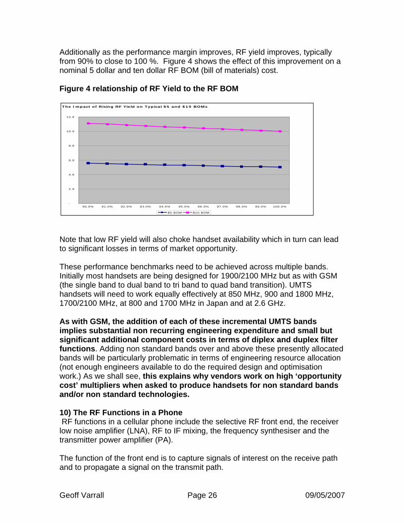
Additionally as the performance margin improves, RF yield improves, typically from 90% to close to 100 %. Figure 4 shows the effect of this improvement on a nominal 5 dollar and ten dollar RF BOM (bill of materials) cost. Figure 4 relationship of RF Yield to the RF BOM The Impact of Rising RF Yield on Typical $5 and $10 BOMs
$5 BOM $10 BOM Note that low RF yield will also choke handset availability which in turn can lead to significant losses in terms of market opportunity. These performance benchmarks need to be achieved across multiple bands. Initially most handsets are being designed for 1900/2100 MHz but as with GSM (the single band to dual band to tri band to quad band transition). UMTS handsets will need to work equally effectively at 850 MHz, 900 and 1800 MHz, 1700/2100 MHz, at 800 and 1700 MHz in Japan and at 2.6 GHz. As with GSM, the addition of each of these incremental UMTS bands implies substantial non recurring engineering expenditure and small but significant additional component costs in terms of diplex and duplex filter functions. Adding non standard bands over and above these presently allocated bands will be particularly problematic in terms of engineering resource allocation (not enough engineers available to do the required design and optimisation work.) As we shall see, this explains why vendors work on high ‘opportunity cost’ multipliers when asked to produce handsets for non standard bands and/or non standard technologies. 10) The RF Functions in a Phone RF functions in a cellular phone include the selective RF front end, the receiver low noise amplifier (LNA), RF to IF mixing, the frequency synthesiser and the transmitter power amplifier (PA). The function of the front end is to capture signals of interest on the receive path and to propagate a signal on the transmit path.
Geoff Varrall Page 27 09/05/2007
The receiver LNA amplifies the signal of interest on the receive path. The mixing process takes the incoming signal and mixes it with a second frequency to create an intermediate frequency (IF) at which the signal will be processed. In Direct Conversion Receivers, the second frequency is identical to the receive frequency but with a 90 degree phase off set. The frequency synthesiser takes the stability of a frequency reference such as a quartz crystal and translates that reference to the required frequency to be demodulated (receive path) or modulated (transmit path). The transmitter power amplifier amplifies the signal to be transmitted. 11) RF Device functionality and useful inventions over the past 100 years For the past 100 years radio devices have been required to oscillate, resonate, filter, switch and amplify. The efficiency with which these tasks are performed defines the overall efficiency of the radio system. Fleming’s thermionic valve in 1904 and Lee de Forest’s triode valve in 1907 were major moments in radio device development. These devices, combined with resistors, inductors, diodes and capacitors provided the basis for Marconi’s development of tuned circuits during the First World War. In retrospect, the discovery of the piezo electric effect by Pierre and Jacques Curie in 1880 was probably at least as significant. The Curie brothers discovered that when pressure was applied to certain crystals, an electrical voltage was generated. Conveniently for the radio industry, this proved to be a bi directional effect. Applying electrical voltage to certain crystals would cause them to vibrate at a specific frequency. In 1917, Paul Langevin used quartz crystals in a sonar device for submarine detection and from then on quartz became the basis for detecting and creating specific audio and radio frequencies. In the Second World War, similar research in the US, Japan and the Soviet Union showed that certain classes of ceramics exhibited piezo electric behaviour. Courtesy of two world wars we were provided with a choice of quartz crystals and or ceramic based devices as the basis for providing accurate frequency and time referencing in radio products. The invention of the transistor in 1947 and the integrated circuit in 1958 used in combination with these devices provided the basis for the power efficient and
Geoff Varrall Page 28 09/05/2007
spectrally efficient radio transceivers which have powered the wireless industry for the past 50 years and the cellular industry for the past thirty years. However 50 years on these RF functions are still typically realised as discrete components, existing along side rather than inside present integrated circuits. 12) Present day issues of RF Device Integration Present day issues of RF device integration are as much mechanical as electrical. Radio reception starts with an antenna. Antennas in hand held devices are either electrical dipoles, small loops, helical, meander antennas or patch antennas. Patch antennas, also known as Planar Internal Antennas are increasingly popular as embedded antennas. Typically these are used with grounding which shifts the antenna resonance to a lower frequency with a slot added to increase electrical length, a design known as Planar Inverted F Antennas (PIFA). Antenna size can also be reduced by using dielectrics with a high dielectric constant. Another option is to use fractal based antenna patterns to use whatever space is available reasonably effectively. However any antenna, when constrained within a space that is significantly less than a quarter wavelength of its centre frequency will be inherently inefficient. There are three significant contributors to this loss of efficiency; The imperfect impedance match of the antenna – especially at the band edges – gives rise to significant reflection loss particularly at lower frequencies (850/900 MHz or below). Ohmic and dielectric losses convert useful RF energy into heat in the antenna and any associated matching circuits. RF currents may be coupled into other components within the handset, dissipating RF energy inside the phone. Candy bar, clam shell and slider phones all have similar but different challenges in terms of antenna efficiency. Some antenna designs in present products when used close to the head have negative gains of -8dB or less. 13) Antennas for Candy Bar Handsets In a simple candy bar design, the impedance of the antenna is a function of the dimension, particularly the length, of the chassis of the phone. The chassis consists of the printed circuit board, the conductive components and assemblies
Geoff Varrall Page 29 09/05/2007
connected to it and any conductive paint applied to the case to enhance electromagnetic compatibility. Figure 5 plots chassis length against bandwidth as a percentage of centre frequency for a -3 and -6 dB return loss. Figure 5 Antenna bandwidth plotted against chassis length (Graphic and data sets courtesy of Antenova) www.antenova.com
The antenna has a typical volume of only 6mm by 40mm by 15mm.This is equivalent to 3.6ml, or 0.00011 cubic wavelengths so unsurprisingly the dominant radiation is from the chassis and not the antenna. The chassis is behaving as a resonant half wavelength radiator, excited by the antenna. 14) Two Part Clamshell Handset Antennas and slider phone antennas Typical clamshells are around 85mm long when folded and 140 to 160mm long when opened. Both dimensions are unfortunate from an electrical point of view. In addition, the current maximum in the centre falls in the region of the flexi PCB (F-PCB) connecting the upper and lower components of the handset. This high RF current dissipates into the flexi PCB and creates unwanted coupling of RF and digital signals. Optimisation requires careful management of the electrical design of the hinge and adjacent ends of the two separate parts of the phone. Figure 6 Equivalent circuit showing the effect of the flexi-circuit and the inter component capacitance (reproduced from Antenova White Paper).
Alternatives to the above could include placing the antenna at the top of the flip or in the hinge. Placing the antenna in the hinge is non optimum in terms of driving radiating current into the chassis. Positioning the antenna close to the flexi circuits driving the camera and display will couple noise into the receiver particularly in the lower operating bands. All options (top flip, centre or bottom flip) are space constrained particularly in small slim devices. Flip phones have the additional problem that the antenna has to centre drive the chassis when open and end drive the phone when closed. Generally the bottom end position provides the best compromise but all options will be influenced by how the user holds the device, the ‘hand effect’. The clamshell handset shown in Figure 7 has its antenna in the thicker lower part of the phone. The user in this example holds the phone in a light grasp which would ensure the highest possible gain from the handset. Figure 7 Clamshell Handset held in a light grasp
Other considerations include the battery which occupies about 1/3 rd of the external surface of most phones. The battery always reduces the radiated signal and functions as a short circuit stub approximately a quarter wave length long. Its presence and the way in which it is grounded will have a strong influence on the radiating currents flowing over the chassis. The design of conductive EMC coatings will also have a significant impact on efficiency. Multi band phones have used various techniques to try and minimise losses caused by unwanted coupling and impedance mismatch effects. Mechanically, the quarter wave half wave relationship between 900 and 1800 MHz has been used to produce single antennas that work across both bands with sufficient bandwidth to cover receive and transmit frequencies In multi mode phones, including phones with Bluetooth and/or Wifi and/or GPS or DVB functionality, the usual approach is to have separate antennas for each
Geoff Varrall Page 31 09/05/2007
radio function. This is particularly important if the functions are being used simultaneously. Antenna design is tricky and becomes trickier with each additional band. The largest single cause of lost efficiency is a large mismatch loss at the antenna input. As handset form factor has reduced (length, width and height) it has become progressively harder to predict and control the impedance bandwidth of the antenna or multiple antennas in the device. If additional frequency bands are introduced, the time for the design and integration of the antenna is likely to rise rapidly or antenna performance on the new bands may be significantly lower than at present. This is particularly true if new frequencies lie significantly below the existing allocations or if it is required to combine additional frequency bands with those already existing. Antenna integration is carried out separately for each handset design and is a relatively expensive process. Handset designs with inadequate production runs will not be of great interest to antenna manufacturers unless the handset manufacturers accept all the increased prototype design costs. A further twist to this aspect is the forthcoming integration of antennas for DVB-H and other broadcast services. The inclusion of antennas for these services will add to the problems of antenna integration and further increase the cost barrier to the integration of antennas for new frequency bands for the ‘basic’ mobile services. The addition of broadcast services places additional constraints on the broadband output noise allowed from PAs. Additional filtering is needed to prevent the TV front end from being blocked by the local transmission. The cost and practicability of these filters depends on the frequency relationship between the edge of the broadcast band and the mobile transmission frequency. Once broadcast facilities have become established it will be increasingly difficult to persuade users that they must give them up in order for a new mobile band to be introduced. In summary, transmit frequencies are being generated in immediate proximity to the receive antenna. Typically transmit power can be 100 dB higher than the received signal of interest. Achieving acceptable isolation between transmit and receive paths can be particularly challenging. 15) The antenna TX/RX switch module for GSM, duplexers for UMTS One solution is not to transmit and receive at the same time. This is used in GSM only phones where there is a two slot off set between transmit and receive frames. Switching is normally implemented with a GaAs device or Pin diodes. WCDMA phones however send and receive at the same time and therefore require a duplexer.
Geoff Varrall Page 32 09/05/2007
GSM/WCDMA phones therefore typically end up with a duplexer and a GSM TX/RX switch in the front end of the phone. Each additional UMTS band requires an additional duplexer. 16) Other front end switch paths In addition, there is a need to band switch and mode switch. In an ideal world you would not introduce these switch paths. They create loss and distortion and dissipate power. More bands and additional modes therefore add direct costs in terms of component costs and indirect costs in terms of a loss of sensitivity on the receive path and a loss of transmitted power on the transmit path. One alternative is to use MEMS (micro electrical mechanical system) based switches. The idea of building micro electrical mechanical switches has been around for twenty years or so but is now becoming increasingly practical and has the benefit of sharing available semiconductor fabrication techniques. MEMS components are manufactured using micro machining processes to etch away parts of a silicon wafer or to construct new structural layers that can perform mechanical and electromechanical functions. A MEMS based switch would have low insertion loss, good isolation and linearity and would be small and power efficient. In addition it is essentially a broadband device. It is electro statically activated so needs a high voltage which is inconvenient but low current (so practical). MEMS devices are sensitive to moisture and atmospheric contaminants so have to be hermetically sealed, rather like a quartz crystal. This packaging problem would disappear if the device could be sealed at the wafer level during manufacture with additional over moulding to provide long term protection. Integrated MEMS devices are therefore a plausible candidate for band switching and mode switching within the next three to five years. TX/RX switching (for GSM or other time division multiplexed systems) would be more ambitious due to the duty cycle requirements but still possible using optimised production techniques. There is also a potential power handling and temperature cycling issue. The high peak voltages implicit in the GSM TX path can lead to the dielectric breakdown of small structures, a problem that occurred with early generations of SAW filters. Because MEMS devices are mechanical, they will be inherently sensitive to temperature changes.
Geoff Varrall Page 33 09/05/2007
This suggests a potential conflict between present ambitions to integrate the RF PA on to an RFIC and to integrate MEMS devices to reduce front end component count and deliver a spectrally flexible phone. The balance between these two options will be an important design consideration. The optimal trade off is very likely to be frequency specific. For example, if the design brief is to produce an ultra low cost handset, then there are arguments in favour of integrating the RFPA on to the RFIC. However this will make it difficult to integrate MEMS components on to the same device. You can either have frequency flexibility or ultra low cost but not both together. 31) Filtering using Surface Acoustic Wave (SAW) and Bulk Acoustic Wave (BAW) Devices SAW filters are a form of MEMS device in that they use semiconductor processes to produce combed electrodes that are a metallic deposit on a piezoelectric substrate. SAW devices are used as filters, resonators and oscillators and appear both in the RF and IF (intermediate frequency) stages of present cellular handset designs. SAW devices are now being joined by a newer generation of devices known as BAW (bulk acoustic wave) devices. In a SAW device, the surface acoustic wave propagates, as the name suggests, over the surface of the device. In a BAW device, a thin film of piezoelectric material is sandwiched between two metal electrodes. When an electric field is created between these electrodes, an acoustic wave is launched into the structure. The vibrating part is either suspended over a substrate and manufactured on top of a sacrificial layer or supported around its perimeter as a stretched membrane, with the substrate etched away. The devices are often referred to as Thin Film Bulk Acoustic Resonators (T-FBAR). The piezoelectric film is made of aluminium nitride deposited to a thickness of a few tens of microns. The thinner the film, the higher the resonant frequency. BAW devices are useful in that they can be used to replace SAW or microwave ceramic filters and duplexers in a single component. BAW filters are smaller than microwave ceramic filters and have a lower height profile. They have better power handling capability than SAW filters and achieve steeper roll off characteristics.
Geoff Varrall Page 34 09/05/2007
T-FBAR filters are presently being sampled for integration into GSM front end modules. The benefit apart from the roll off characteristic and height profile is that BAR devices are inherently more temperature resilient than SAW devices and are therefore more tolerant of modules with densely populated heat sources (transceivers and power amplifiers). However this does not mean they are temperature insensitive. BAR filters and SAW filters all drift with temperature and depending on operational requirements may require the application of temperature compensation techniques. A typical BAW duplexer takes up a footprint of about 5 by 5mm2 and has an insertion height of 1.35mm. In the US PCS band or 1900/2100 band these devices have an insertion loss of about 3.6 dB on the receive path and 2.7 dB on the transmit path and deliver RX/TX isolation of 57 dB in the TX band and 44 dB in the RX band. More miniaturised versions (3.8mm by 3.8mm) are under development. (reference 8). 18) MEMS resonators MEMS are also being suggested as potential replacements for present quartz crystal based sub systems. The potential to use micro electrical mechanical resonators has been the subject of academic discussion for almost 40 years and the subject of practical research for almost as long. The problem with realising a practical resonator in a MEMS device is the large frequency coefficient of silicon, ageing, material fatigue and contamination. A single atomic layer of contaminant will shift the resonant frequency of the device. As with MEMS switches and filters, the trick is to achieve hermetically robust packaging that is at least as effective as the metal or ceramic enclosures used for quartz crystals but without the size or weight constraint. There are products now available that use standard CMOS foundry processes and plastic moulded packaging. These devices are not yet sufficiently developed to be used as a replacement for a GSM or CDMA TCXO but they potentially offer significant space and performance benefits. A MEMS resonator is a few tenths of a millimetre across. A quartz crystal is a few millimetres across, one hundred times the surface area. MEMS resonator performance is a function of device geometry. As CMOS geometries reduce, the electrode gap reduces and the sense signal and signal to noise ratio will improve, giving the oscillators a better phase noise and jitter specification. As MEMS resonators get smaller they get less expensive. As quartz crystals get smaller they get more expensive. MEMS resonators therefore become increasingly attractive over time (Reference 9).
Geoff Varrall Page 35 09/05/2007
19) MEMS based duplexers As profiled in our introduction, MEMS based tuneable capacitor arrays may provide the basis for multi band digital duplexers but such solutions are not presently available for mass market deployment. 20) Implications for future radio systems It seems inevitable that the regulatory environment will require the industry to produce handsets that are capable of working across ever more numerous multiple bands and that the standards making process will ensure that handsets will also have to support ever more numerous multiple radio standards. This increases RF component cost and makes it harder to deliver consistent RF performance across such a wide range of possible RF operational conditions. This trend also highlights that some of the traditional RF device technologies that have served us faithfully for 50 years or more are non optimum for these extended operational conditions. From a business perspective, there is evidence of a closer coupling between companies with antenna and shielding expertise and silicon vendors (reference 10). Similar agreements are likely between the MEMS community and silicon vendors to meet the perceived 3 to 5 year need for a closer integration of RF MEMS functionality with next generation silicon. At that stage, but not before, the software defined radio finally becomes a practical reality. Long term reliability issues of MEMS devices (given that they depend on mechanical movement) also still need to be resolved. (Reference 11) 21) Present Handset status We said that we would use present Dual Band/TriBand/Quad band as an example of the RF architectures, integration levels and partitioning used in present GSM cellular handsets. We need to place this in the context of the present bill of materials for a GSM quad band handset, how this BOM has reduced over the past three years and what the RF BOM might be in 3 years time Additionally it would be useful to show whether over time the RF BOM is increasing or decreasing or staying constant as a percentage of the overall BOM of the phone. From this we can calculate the incremental RF component cost of supporting additional non standard bands in present single mode quad band GSM phones. We then need to calculate the incremental RF component cost of supporting additional non standard bands in dual mode GSM/UMTS phones.
Geoff Varrall Page 36 09/05/2007
Finally we should calculate the incremental RF component cost of supporting additional non standard bands in UMTS only single mode phones. Table 4 shows the RF BOM for a tri band phone three years ago costed on the basis of one million units per annum, all in dollars. Table 4 RF BOM of a Tri Band GSM handset in 2003 Component Quantity Cost in dollars RF VCO 1 .94 TXVCO 1 1.6 RF balun* 1 0.09 Dual digital transistors 4 0.18 TCVCXO 1 1.53 Tri band transceiver 1 2.32 RF front end module 1 2.19 Transmit power control IC 1 1.08 Triple band power amplifier
1 2.48
High speed LDO** (2 V voltage regulator)
1 0.11
Total 12.52 dollars *Balun – Balanced Unbalanced – a device used to convert an unbalanced line to a balanced line, for example between a twisted pair (balanced) and a co axial cable (unbalanced). **LDO stands for 'low drop out'. In order to regulate and give a stable voltage output, the input voltage must be higher than the output voltage. LDO refers to how near (low) the input voltage can approach the output voltage and the output regulation still remain in specification. The total RF BOM cost of $12.52 dollars includes software costs for the module. If the volume reduces to 250K, the production cost doubles (reference 12) The RF BOM represented 7% of the total materials cost (180 dollars) with the main cost elements being the screen (50%) and baseband (13%). Note this was a relatively high end phone with (at the time) relatively advanced multi media functionality. Today in 2006, a comparative device, admittedly quad band rather than tri band would be about 6 dollars costed on a similar volume and the RF BOM would still be about 7% of the total bill of materials (reference 13) In three years time, some vendors are suggesting that the RF BOM cost will halve again to 3 dollars so the RF BOM would be 10% of a 30 dollar handset (for the ULCH market) or approximately 7% of a 40 dollar handset. This will only be achieved if it proves feasible to integrate the PA and/or front end matching in to the RFIC. The present premium being paid by network operators for a dual mode handset is between 30 and 50 dollars. Part of this premium (about 6 to 10 dollars) is the
Geoff Varrall Page 37 09/05/2007
additional RF BOM, part of the premium is due to patent costs and the remainder are baseband and MMI costs (man machine interface components such as the display). The RF BOM premium is made up of a front end duplexer, required instead of the antenna switch used in GSM to separate out the transmit and receive frequencies within bands and a more linear more expensive PA. Note that certain GSM handset classes (GPRS Class 13 to 18) also require a duplexer so the duplexer premium would apply to both devices though at time of writing no Class 13 to 18 handsets have been brought to market. However substantial caveats need to be applied to these cost guidelines. UMTS volumes are only just getting to the point where non recurring engineering costs are being recovered and it is reasonable to expect rapid real cost decreases in UMTS component costs over the next three to five years. Specifically it would be reasonable to expect the UMTS RF BOM to reduce to 6 dollars in 3 years and 3 dollars within 6 years, in other words to follow the GSM cost reduction curve. There are counter arguments to these assumptions. For instance shortages of raw materials, particularly rare metals, are becoming increasingly common heightened by the present demand curves for consumer goods in China and other fast growth global markets. The recent purchase of substantial stake holdings in Freescale Semiconductor and NXP by venture capital investors suggests the investment community at least is confident that silicon demand is likely to increase faster than supply. This may have a significant future effect on critical component costs. 22) Present RF BOM cost optimisation for ULCH (Ultra Low Cost Handsets) Direct RF BOM costs are also only part of the story. What we really need to know are the typical manufactured costs and this depends on other factors including RF yield, RF calibration and RF test on the production line. A case study of a present GSM quad band phones highlights some of these issues. Figure 8 GSM quad band transceiver block diagram – with thanks to Silicon Laboratories
Figure 8 shows typical present partitioning with (from left to right) the antenna, antenna switch, SAW diplex filters for the 4 receive bands and an RF PA for the four transmit bands. All other functions are on the RF IC with the exception of the reference oscillator. In the receive path, the antenna switch (ASM) directs the incoming signal from the antenna to the appropriate surface acoustic wave (SAW) filter for frequency band selection. These components introduce an insertion loss (IL) to the received signal and are therefore in effect part of the link budget. There is a need to input match between the SAW devices and the low noise amplifier input to maximise the power or voltage transfer. The transceiver then either down converts the RF signal to an intermediate frequency (a traditional superhet architecture) or converts the signal directly to DC (direct conversion receiver) and then selects the proper receive channel. The signal is degraded by noise introduced by the low noise amplifier. The lower the noise floor of the transceiver, the easier it is to trade off cost and insertion loss in the ASM (antenna switch) and SAW filters. For instance two SAW devices can be combined into a dual SAW module achieving a 20% cost reduction and a 45% saving in space on the PCB. The ‘cost’ is an increased insertion loss and pass band ripple that may affect system sensitivity and reduce blocker attenuation which may potentially affect GSM full type approval (FTA). However for transceivers with ample noise floor margin and strong blocking performance, these potential effects are likely to be imperceptible at system level.
Geoff Varrall Page 39 09/05/2007
An adequate noise floor margin also allows designers to use lower cost multi layer ceramic (MLC) inductors for the LNA input match instead of wire wound or coil inductors. The MLC inductors have a reduced Q but achieve a 75% cost reduction. The Q problem is insignificant provided the transceiver has a low noise floor and is designed specifically for a low Q input match. At the reference oscillator interface, transceiver timing is synchronised to an external crystal based source. The transceiver then provides a system clock to the baseband. Expensive voltage controlled, temperature-compensated crystal oscillator (VC-TCXO) modules were traditionally used to maintain target oscillator frequency. 23) Lower cost oscillators There is however now a trend to using smaller lower cost alternatives to the VC-TCXO, either voltage controlled crystal oscillators (VCXO) or fully integrated digitally controlled crystal oscillators. The VCXO replaces the VC-TCXO with a standard AT-cut crystal, varactor and capacitors but the biggest BOM reduction is achieved by using an integrated DCXO, integrating all external components except a 3.2 by 2.5mm crystal costing $0.35. Integration eliminates the need for varactor calibration on the production line and the approach achieves a significant saving over the VC-TCXO (presently costing $0.95). Space savings are also achieved on the PCB. 24) Production test times and costs We referred earlier to the relationship between RF yield and RF BOM cost. A transceiver design and components that improve handset yield by 1% will effectively shave off $0.30 off the cost of a $30 handset, $0.60 off a 60 dollar handset and $1.20 off a $120 handset. Additionally, the manufactured cost needs to include test times on the production line which are presently about 60 seconds for a GSM phone and 150 seconds for a UMTS phone (Reference 14). Each additional band covered adds approximately 25% to this test time. The cost per second depends on individual vendor production economics. One suggested cost metric (Reference 15) is that every second of test time saved translates into a 2 cent saving per phone so on this basis an additional band adds 30 cents of production test cost to a GSM handset and 75 cents to a UMTS handset. So the answer to the question of how much additional recurring cost is introduced to the RF BOM when an additional band is added is about two dollars on a 6 dollar RF BOM reducing to 1 dollar on a 3 dollar RF BOM.
Geoff Varrall Page 40 09/05/2007
This is based on a baseline of 1 million units per year but doubles if the volume reduces to 250 K. Note that it may be problematic to achieve a satisfactory RF yield at these low market volumes. Over and above one million units per year, the premium on component costs will reduce marginally with volume. For the purposes of our economic model we estimate that this will reduce to one dollar on a 6 dollar RF BOM and 50 cents on a 3 dollar BOM and have set a nominal volume of 5 million units per year at which this price stability is achieved. The baseline is the additional SAW filter in the RF front end, additional matching components and additional test time on the production line. 25) Additional Nuisance Costs Note that there are additional ‘nuisance costs’ to be factored in to the component cost equation. Neither silicon vendors nor handset manufacturers particularly want to support products that are country specific. From an operator’s perspective it is problematic to explain to users that they cannot use phones imported from other countries unless they support the country specific band allocation. The only answer to both these problems is to include the additional band support in all handsets though the practicability of doing this depends on the relationship between the added band and the pre-existing bands. A one dollar cost premium on, say 50 million handsets per month implies that the real cost to the industry of supporting a non standard country specific allocation will be 50 million dollars per month. The effects of amortising this over country specific market volumes are shown in the ‘Economies of scale’ summary at the end of this document. 26) Additional RF BOM implications of GSM/Dual mode Handsets Adding UMTS to a GSM handset increases the RF component count by anything between 55 and 175 components (Reference 16). Present GSM handsets have a front end switch, typically a GaAs device, performing the function of a duplex filter. The exception would be Class 13 to Class 18 GPRS handsets which have overlapping time slots but in practice none of these phones have been introduced to the market. UMTS handsets transmit and receive at the same time so need a duplexer to separate transmit and receive paths within each band. These devices have significant insertion loss (2 to 3 dB), are bulky and increase the component cost. FBAR based solutions are being introduced which are smaller. An example is an FBAR Quintplexer (Reference 17) introduced for multi band 850/900/1800/1900 MHz transceivers integrated with a GPS receiver.
Geoff Varrall Page 41 09/05/2007
The example device is packaged in a 5mm by 8mm by 1.3mm module. The loss at 850 MHz is 2 dB and 3 dB at 1900 MHz and the cost is $3.75 in quantities of 5000. So BAR devices help resolve the space issue but still introduce insertion loss and cost. Each additional band requires an additional BAR filter. Prices for higher volumes would be substantially lower than the $3.75 quoted above but will still represent a significant percentage of the overall RF BOM of the device. In larger volumes it is reasonable to calculate that the additional duplexing cost overhead per band for UMTS will be between 1 and two dollars over and above the cost of the broad band antenna switch module used in GSM. Each additional band also requires a diplexer, traditionally a SAW filter. Figure 4 shows the four SAW filters needed for Quad band GSM. Each SAW filter needs LNA matching components. For quad band, the additional component count will be 16 components plus four components for each additional band. Modules are available from Fujitsu, Murata, Sawtek (now Triquint) and Epcos , typically within a footprint of about 5mm by 3mm which integrate the SAW filters and matching components into one package. In order to make a match to the LNA, the transceiver supplier needs to provide accurate S parameters for the LNA input including bond wire and package parasitics to the module manufacturer who then makes a custom part which mates with the specific integrated circuit. Testing and validation then has to be done jointly by the two suppliers, with the solution evaluated as a reference design. Thus the incremental recurring costs implied by supporting an additional band may seem relatively trivial (between one and two dollars per phone for a cost optimised, space optimised and performance/insertion loss optimised solution) but the availability of such a solution is dependent on having sufficient volume to interest the SAW and/or BAR/FBAR module vendors to undertake the required design work. There is therefore a direct trade off between recurring costs (component ‘technology’ costs per unit) and the non recurring ‘engineering’ costs needed to develop these components. 27) An example from the 1.7 GHz Band in Japan An example would be the 1.7 GHz UMTS band in Japan. Murata have optimised SAW diplex and SAW duplexer products for this band. The SAW diplex filter is 1.35 by 1.05 by 0.6mm, the SAW duplexer is 3.00 by 2.5 by .8mm. The SAW duplex filter has a harder job to do than the SAW diplexer in that the separation (in this example) is 95 MHz compared to say the 900 MHz of separation between two diplexed bands at 900 and 1800 MHz.
Figure 9 Comparisons of a SAW diplexer and SAW duplexer product from Murata for the 1.7 GHz UMTS Band in Japan (announced August 24, 2005) Reference http://www.murata.com/ninfo/nr0581e.html
Murata however suggest initial production volumes of 2 million per month for the SAW duplexer and 4 million per month for the SAW filters which provides some indication of their minimum volume expectation. 28) Antenna Costs The antenna cost metrics associated with supporting additional bands are similar to SAW filters (antennas are after all a form of resonant filter). Typically today, a 900/1800/850/1900 MHz phone will have a multi resonance antenna or an antenna split into two or three separated feed points. This principle could be extended to include the 2.6 GHz and 3.5 GHz bands. The mechanical/electrical design options involve either creating a multi resonance or switch able structure within a very small volume or to fit two or three antennas into the same volume though this has associated problems of isolation and interaction between the antennas. The lower bands, for example lower band UHF at 500 and 600 MHz are particularly problematic due to the required resonant length. There are also specific form factor issues (candy bar, clam shell, slider) discussed earlier. Thus an antenna to support a new band might add a component cost of a few cents per phone but will require significant engineering investment in order for the solution to be cost and performance efficient within the prescribed mechanical form factor constraints. (Reference18) 29) Cost and performance metrics In corroboration of the above, the following ‘good practice’ guidelines were offered by a PA vendor (Reference 19) ‘Watch out for the increased loss between the PA and antenna when increasing the bands or adding a duplex filter (for example for UMTS). This will increase TX power generated and reduce talk time. One needs to be careful also about the additional heat generated in small phones. If standard IC’s cannot be used for the non standard solution, the size of the radio will be substantially greater, over 4 times. The cost of the non standard solution is going to be driven by the development cost and the semiconductor company recovering its development cost.
Typically this development cost will need to be recovered by a factor multiplier of between 10 and 20 as a lost opportunity adder in addressing low volumes (studied in more detail in the next section) The designer needs to consider the effect of additional losses between the antenna and the power amplifier and the related impact on talk time. Some additional band flavours may require non standard PA’s to overcome these losses. Using a duplex filter in a refarmed handset will introduce a dB or more additional RF loss to the antenna than with a standard GSM handset. This will impact talk time and may create heat dissipation issues. Without economies of scale, the level of integration will be less. The area and cost of the radio circuits will significantly increase. The following applies to each of the four functional areas in the handset: RF Front end The antennas, switch, duplexers and diplexers are the major space users, the antenna first. The cost versus volume trade offs are acute for the duplexers. Diplexers are easier to implement in a small size. Receiver LNA This is a lower cost circuit to develop. In high volume applications it is very small and integrated in to the chip set. It may well be external to the chip set for a low volume solution which is using existing chips to cover the bands. This will push up size and increase the BOM by up to say $0.5 dollars. Frequency Synthesiser Phase locked loops and VCO’s SHOULD (famous last words) be able to cover all the frequency bands. New tuner IC’s have greater agility than previous IC’s. If standard transceiver chips are not acceptable, the solution will be very discrete and increase size by a factor of four and cost by a factor of 10. Transmitter PA The first issue is not to increase the loss to the antenna. The next issue is to keep the PA bandwidth as narrow as possible to help with the efficiency (the wider the bandwidth the more imperfect the match). The following table summarises present PA technology options and their relative merits/demerits Table 5 Comparison of PA process technologies Technology Performance Cost Development Time Development
Cost GaAs RF highest Highest Shortest (best RF
performance, shortest time
Least, for RF changes only, fewer masks and
Geoff Varrall Page 44 09/05/2007
through fab provided it uses the same CMOS controller IC
larger geometry
SiGe 2% less efficient than GaAs at higher powers Competitive efficiency at lower powers
Integration dependent but less than GaAS and GaAs controller IC
Longest fab time 10-12 weeks
Significant – greater than $500K for new minor variants
CMOS 5% less efficient in GMSK mode than GaAs at maximum power. Efficiency competitive at lower power or when handling AM modulated signals
Lowest by far. 30% less than SiGe
Middle of the two, shorter than SiGe as fewer processing steps involved. Requires more suppliers/experience to be fully exploited
Significant. Greater than $500K for a new minor variant
The above shows that the choice of PA technology will have an impact on both NRE cost and component cost. If the PA manufacturer has invested one million dollars in investment, he will want sales of 20 million dollars as a minimum. So for a 2 million unit market, the minimum cost per PA is $10 dollars. For a 200 million unit market, the NRE investment disappears in the noise floor.’ This relationship between NRE cost and the ongoing BOM cost is covered in more detail in the next section. There are significant differences of opinion as to the real cost differences between these technologies. Vendors promoting CMOS RF synthesiser and transceiver devices will generally highlight the reduction in discrete components in the front end, typically from about 60 down to 15 and the related indirect costs savings achieved by not having to stock, manage, insert and test those components. The argument therefore is that overall cost savings will be a composite of these direct and indirect costs. Given that the discrete front end components are generally frequency specific this would suggest direct and indirect incremental costs for an additional band will be lower with CMOS than with GaAs or SiGe. However achieving these savings will incur substantially higher non recurring engineering cost. 30) Dual band versus tri band versus quad band price differentials
Geoff Varrall Page 45 09/05/2007
Summarising the above, as might be expected, we have had a spread of responses on RF BOM price points and some differences of opinion on future trends. One tier one silicon vendor confirmed the view that quad band GSM represented the most cost optimised and performance optimised product presently available. The volume and inventory savings could be regarded as more than off setting the additional SAW diplex filter costs. Alternative vendors have suggested that this is probably only true if the customer (the handset manufacturer) absorbs the risk of device integration. A tier 1 RF PA vendor (reference 20) comments as follows ‘The RF BOM price point for quad band GSM of 6 dollars is OK but too high for dual band or tri band. Dual band is about 2/3rds of the 6 dollar price, in other words just under four dollars. So this would suggest simplistically (at least for the purposes of economic modelling) that the dual band RF BOM is about 4 dollars, tri band about 5 dollars and quad band 6 dollars. The ‘dollar difference’ is partly due to the additional direct and indirect cost of the SAW diplex filters (a few cents) but is primarily dependent on the quality regime required by the customer. If a silicon vendor is asked to support an additional band, they take on the risk of working with the customer (the handset manufacturer) in terms of characterising the device so that it will arrive at the end of the customers production line having met specific cost and performance targets, including for example handset to handset/ batch to batch best to worst performance spreads. This quality regime risk determines the price point. Tier 2 or tier three handset manufacturers have a habit of wanting to negotiate lower BOM price points but are also prepared to accept a laxer quality regime but this implies that these products will be less consistent in terms of their RF performance. Basically you get what you pay for. Quad band could potentially be considered as being capable of reaching a parity price to tri band or dual band if the inventory savings outweighed the additional SAW diplex filter costs but this would only be possible if the customer (the handset manufacturer) was prepared and able to take on the quality regime risk and amortise it over such a large volume that it effectively disappears. If the handset manufacturer takes on the quality regime risk, the RF BOM will be lower but the cost will reappear in the composite manufactured cost of the handset. Some of the future anticipated RF BOM savings needed to meet ULCH cost price points assume a single chip RFIC and a number of vendors are promoting this as a preferred way forward. However the power dissipation with GSM can be one and a half watts (at 55% efficiency) and similar for WCDMA (250 milliwatts but a continuous duty cycle and lower efficiency) and it is inconceivable that this device will perform well on the same die as baseband and mixed signal functions.
Geoff Varrall Page 46 09/05/2007
Despite present vendor claims, it is likely that the RFPA will remain a separate component for the foreseeable future (certainly for more than 5 years ahead). Claims by vendors that single chip including RF will be deliverable on CMOS within three to five years assume that RF performance requirements will remain similar to present day expectations. In practice, RF performance expectations for the RFPA in terms of parameters such as error vector magnitude and ACPR will have moved on significantly so will represent a moving target which will be hard to hit. On future RF BOM cost trends there is a real price pressure to reduce ASP by at least 15% per year. Tier 1 silicon vendors cannot afford to let this happen so work to acquire other people’s value (through integration) and add value through additional functionality and performance (better sensitivity and selectivity or data rate or channel flexibility) to keep the ASP constant. This is a market dominated by at most five vendors in any particular application sector. For example, the cellular RFIC business is almost completely in the hands of three, at most four vendors. As such this is a classically mature market where pricing behaviour remains relatively stable over time. There are potentially interesting innovations such as RF MEMS which will deliver a measure of spectral flexibility over time and useful performance gain, for example the ability to deliver broadband matching from 500 MHz to 4 GHz on the transmit path with relatively high efficiency. However the suggestion by RF MEMS vendors that these devices will be available within three to five years is significantly over optimistic. Present R and D validation suggests there may be some sampling of integrated RF MEMS devices within 5 years but real product is 7 to 10 years away ’ The above suggests that it will be harder than expected to meet ULCH handset cost targets in GSM and that it could potentially be easier for most vendors if these products were dual band or at most tri band devices and certainly not devices that have to support additional non standard bands. It also corroborates the view that GSM may be getting close to its lowest achievable cost floor which leads us to our next topic. 31) GSM versus UMTS cost cross over points Superficially it might seem that UMTS will always have an intrinsically higher RF BOM than GSM due to the increased linearity required both on the transmit and receive path and the additional duplex filtering requirement for each band supported in the device. There are also presently more rigorously contested intellectual property rights on UMTS phones that add to the combined RF and baseband BOM. Table 6 Simplified RF channel spacing by generation Spectrum Channel Number of RF
Geoff Varrall Page 47 09/05/2007
spacing channels 1G ETACS 33 MHz 25 kHz 1321 AMPS 25 MHz 30 kHz 833 2G GSM 900 39 MHz 200 kHz 195 GSM 1800 75 MHz 200 kHz 375 3G UMTS FDD 60 MHz 5 MHz 12 UMTS TDD 35 MHz 5 MHz 7 However Table 6 (above) and Table 7(below) illustrate that in practice the RF implementation of a UMTS phone and other wide band variants would be/will be simpler than a GSM phone in terms of the number of channels supported and the channel spacing. Decreasing the number of channels supported simplifies the design and function of the frequency synthesiser. Increasing the channel spacing relaxes the need for RF reference stability and RF channel to channel selectivity. (For a more detailed treatment of this topic go to Background Notes on Technology, section 2 on the special case of OFDM frequency stability.) Table 7 UMTS, WiMax and UTRAN/LTE channel spacing Cellular 1G 2G 3G UTRAN LTE 25/30 kHz 200 kHz 5 MHz Scalable
from 1.25 to 20 MHz
WiMax Scalable from 1.25 to 20 MHz
Scalable from 1.25 to 20 MHz
Additionally Release 6 and Release 7/UTRAN LTE reduces the requirement for a large dynamic range (the need to implement slow and fast power control over an 80 dB power range) on the downlink though the dynamic range requirements on the uplink stay the same (users have to be ‘seen’ at the base station at near equivalent power levels). Overall we would offer the argument that a single mode UMTS/UTRAN LTE handset could potentially have a lower RF BOM or certainly an equivalent BOM to a present GSM quad band cellular handset. We would however also argue that the RF BOM will probably still be about 7% of the total handset BOM in that higher specification handsets will have higher specification RF functionality, for example high data rate optimised multiple parallel receiver front ends (advanced receivers), multiple parallel transmitter architectures and integrated wide area, local area (WiFi) and personal area (Bluetooth and UWB/WiBree and NFC) functionality. The point at which this price parity is achieved is open to debate. For the purposes of our economic model we have taken the proactive view that assuming present IPR issues are resolved, price parity with present GSM
Geoff Varrall Page 48 09/05/2007
handsets will be achieved within two to three years from now. This in turn assumes that the ‘cost add’ of linearity will be offset by the cost reduction achieved through relaxed channel spacing and that the ‘cost add’ of duplexing will have been neutralised by the adoption of digital duplexing techniques. It is however hard to do like to like comparisons between GSM and UMTS. For example, the RFBOM for UMTS will be dependent on the handset class which in turn determines the transceiver architecture. An example of a presently ambitious UMTS design would be a Category 9 HSDPA handset with advanced receiver functionality. The advanced receiver implies a dual antenna front end to support full receive diversity. This type of device would have a substantially higher RF BOM than standard GSM and a DC power drain that would make it better suited to a lap top form factor rather than a slim handset design implementation (reference 21). Additionally, it may take significantly longer for digital duplexing techniques to be realised than present vendor statements would suggest. This, coupled with the probable need to keep the RFPA off chip would suggest that adding incremental bands to UMTS may be problematic both for ‘basic phones’ and for phones with more advanced receiver functionality.(See Technology background 11 and 12 for a more detailed treatment of this topic). CHAPTER 3 Non Recurring Engineering Costs 1) Non Recurring Costs and their impact on RF BOM costs for limited volume markets So far in this study we have concentrated on recurring costs, the component costs of present cellular handsets, future trends and most importantly for this study, the incremental component cost implications of implementing non standard bands. We have said that there is presently a substantial RF BOM differential between GSM and UMTS but that this could erode to parity over the next two to three years. Front end integration potentially lowers the component cost penalty of non standard band deployment though integration of duplex functionality (the ability to separate signals that can differ in power level by 100 dB or so) will remain challenging in terms of RFIC integration. The integration of power amplifiers onto RF integrated circuits will be similarly challenging. It is arguably easier to achieve more aggressive integration with a GSM only handset than with a dual mode GSM/UMTS or single mode UMTS handset. It is this assumption that is presently driving vendor efforts to realise highly integrated ultra low cost GSM handset platforms. (Reference 22)
Geoff Varrall Page 49 09/05/2007
Early iteration UMTS phones have also tended to have a traditional superhet architecture, sampling at baseband and have been slower to adopt direct conversion than GSM. This is partly due to the requirement to optimise UMTS RF performance for Release99 handsets but also because to date UMTS has only been implemented in one band (1900/2100). There are still significant differences between optimised low cost GSM voice handsets and EDGE and UMTS handsets. The off set phase lock loop technique used on the GSM TX side for example is unsuitable either for EDGE or UMTS However generally it can be considered that the present architectural differences between GSM and UMTS handsets will reduce over the next two to three years reducing the rationale for the present UMTS cost premium. GSM does not have the duplex cost overhead (except for Class 13 to 18 GPRS handsets that are in any case not presently available) but additional band allocations do require additional diplex (band to band) filtering and matching components. We have suggested that the cost premium excluding NRE cost recovery is in real terms approximately two dollars on a 6 dollar BOM in terms of raw material cost and associated indirect costs (costs of handling and testing additional front end discrete components). If the GSM RF BOM were to continue to reduce at the same rate as it has reduced for the last three years, the RF BOM would have halved from 6 dollars to 3 dollars and the cost premium excluding NRE cost recovery would in real terms be approximately one dollar (on the three dollar BOM). This decline in RF BOM may not actually happen due to material and supply constraints and a parallel increase in RF performance expectations, particularly the need to meet user expectations for higher data rates (GSM with EDGE for example). However recurring cost metrics have to be validated against the non recurring engineering costs needed to realise cost and performance efficient components which can be used to create a cost and performance efficient transceiver for a specific band. 2) Quantifying NRE Costs NRE costs are incurred at a number of stages in the product development cycle. For simplicity, we allocate costs in terms of costs predominantly incurred by silicon/semiconductor/component vendors, costs that are incurred by handset manufacturers and costs that are incurred by network operators. We need to establish volume thresholds at which an ‘efficient’ market is achieved in terms of competition between a sufficient number of vendors and the ability of those vendors to achieve a satisfactory return on investment.
Geoff Varrall Page 50 09/05/2007
Table 8 NRE Cost and the industry value chain Silicon/component vendors
Handset Manufacturers
Network Operators
Tier 1/Tier 2/Tier 3 Tier 1/Tier2/Tier 3 Tier1/ Tier 2/Tier 3 Typical NRE investment needed to produce a band specific RFIC is $3 million dollars
Typical NRE investment needed to take that RFIC and produce a band specific handset is $2 million dollars
Typical NRE needed to drive test and interoperability test a band specific handset is $1 million dollars
In this next section, we work through the non recurring RF engineering costs which would be incurred to bring a present cellular phone to market supporting an additional non standard band. We show that the total NRE for adding a non standard band to a handset is at present at least $6 million dollars. An assumption is that RFIC integration levels will increase over time. For example duplexing and diplexing may be integrated on to the RFIC using MEMS based technology. In the longer term, the RF PA may also be integrated. Our contention is that this does not necessarily reduce the non recurring engineering cost but rather shifts some of the cost (and risk) from the handset manufacturer to the silicon vendor. In theory, a more highly integrated RFIC will be more amenable to software configuration. In practice, these devices will need to be precisely pre-configured in terms of their circuit layout and hardware configuration in order to meet specific signal isolation requirements. So the contention is that the risk and NRE cost over time for supporting a non standard band will remain relatively stable over time (and may increase). However the entities undertaking the risk will change. At this point it is probably worth reviewing how the RF section of a cellular phone is designed, who incurs the NRE costs and how the NRE costs translate into finished product price points. Price and cost are of course interrelated but separate and dependent on vendor specific return on investment policy. The return on investment policy effectively determines the difference between materials cost and the price charged for the device.
Geoff Varrall Page 51 09/05/2007
In order to study this relationship between cost and realised price we need to study the present competitive structure of the industry. To establish a credible economic model it is necessary to consider not only the number of vendors but the relative sizes of those vendors by market volume and value. 3) Defining and differentiating Tier 1, Tier 2 and Tier 3 vendors Silicon vendors, handset manufacturers and network operators can be conveniently divided into three tiers in terms of their size and market leverage. Tier 1 players are dominant in multiple markets, tier two are dominant in one or more discrete markets (by region or product sector), tier 3 have not yet achieved dominance either in their local market or other markets. Efficient competition (Reference 23) implies multiple vendors in each tier but an efficient market requires sufficient volume per vendor to provide a sufficient return on investment. The combination of these two requirements produces a market that is ‘supply efficient’. In a supply efficient market, prices have a relatively direct relationship to costs. For the purposes of our volume threshold model we look at the market volume needed to sustain four to five vendors per tier. This implies that a minimum of between twelve to 15 silicon/component vendors and a minimum of twelve to fifteen handset manufacturers is needed per market to achieve ‘supply efficiency’ provided this is combined with a sufficient volume per vendor to meet individual vendor return on investment expectations. 4) Silicon/component vendor NRE We can test these assumptions of supply efficiency for each stage of the supply chain. Let the assumption be that there are five possible silicon vendors who are potential suppliers of an RF IC capable of covering quad band GSM/UMTS, UMTS1900/2100 and an additional band. The process involved is that a mask needs to be generated for the transceiver functions of the device. This will require a team of several dozen engineers working on the project over a number of months. (Reference 24) The silicon vendors may have their own foundry and/or a choice of three or four third party foundries capable of supplying the wafers needed to produce the RF IC. The mask cost will be not less than one million dollars at present geometry
Geoff Varrall Page 52 09/05/2007
levels and the related engineering development costs will be not less than 2 million dollars. These NRE costs will increase with future geometry scaling. The decision will have been made as to what is included and what is not included on the RFIC and the device will have been designed to work with a number of external devices, for example CMOS or GaAS based power amplifier vendors, SAW or FBAR filter vendors, GaAs or CMOS based multi mode RF switch vendors and (for GSM) GaAs based TX/RX switch vendors. The silicon vendors will be expected to produce reference designs that help the handset manufacturer to integrate the RFIC into a handset design.
The expected performance of the reference design will need to be stated including noise figure, second order and third order intercept points and tested to show that a finished product will easily meet specification. For quad band GSM this requires a test of the design coupled with a baseband chip set and GSM protocol stack using a radio communication tester to ensure bit error rate targets are met under specified operating conditions. These test units, available from multiple vendors, will perform automated tests over the (975 Quad band) GSM channels including spurious emission measurements, receiver blocking, AM suppression, intermodulation and adjacent channel selectivity. As stated earlier, a good reference design will typically have about -110 dBm static sensitivity. Even allowing for a 3dB signal to noise margin for fading; the design will be well within the conformance requirement.
Similar measurement on the transmitter for phase errors will typically show significant performance margins over and above conformance requirements.
The reference design will then have been validated as being capable of meeting all relevant type approval requirements.
Note that GSM type certification costs are higher than UMTS partly due to the duplication of certification authorities. The PTCRB (PCS Type Certification Board) manages certification for the US PCS market and is a separate entity to the Global Certification Forum for European and Rest of World markets and to the 3GPP (3rd Generation Partnership Project) certification process.
Thus phones supporting additional non standard band allocations will need to go through these multiple certification processes in order for them to be used and sold legally in other ‘standard band’ markets.
5) Handset Manufacturer NRE including conformance testing Reference designs have to be made into finished products by the handset manufacturers. The amount of work done independently of the silicon vendor will depend on the size (tier1/2/3) and resources and policy of the manufacturer but
Geoff Varrall Page 53 09/05/2007
generally most manufacturers will budget for a team of engineers to manage a project over a number of months. A Tier 2 handset vendor (reference 25) suggests the following hypothetical case study for a typical NRE budget Assume a network operator has asked for a phone for the UHF 470/862 MHz band. For a handset vendor, supporting a new standard band implies a new front end, a new board layout (typically a four or 6 layer PCB), changes to the synthesiser, and possibly changes to the LNA and PA. There will also be small but important changes to make to the layer 1 software in the baseband chip. The RF board layout is fairly straightforward and would take a team of 5 engineers three to four months. The phone however then has to be taken through the conformance test process and prepared for manufacture. As a tier 2 handset manufacturer, a reference design might be appropriate but it would be likely that some sourcing or component choices might be changed for sourcing, operational or design reasons. A tier 3 handset manufacturer would be more likely to follow a reference design more closely. Antenna integration imposes a significant amount of NRE, especially for complex handsets with extensive integrated facilities (cameras, MP3 players and so on). As well as the costs of antenna work, the close association between antenna performance and overall handset design often requires that a handset design is re-spun in order to increase the its overall RF performance. Such re-spinning becomes more likely the nearer the required RF performance lies to the limits determined by antenna volume and its proximity to nearby components. A tier 1 handset manufacturer would effectively be working to their own reference design, but might negotiate specific implementation support from the silicon vendor and other component vendors and would certainly negotiate advantageous component pricing and component supply assurance on the basis of offered volume. Tier1, Tier 2 and Tier 3 manufacturers would in common have to take the final design through the conformance test process. Our tier two vendor taken as an example would therefore budget for three stages, the RF board layout and device integration, conformance testing through
Geoff Varrall Page 54 09/05/2007
a third party test house and preparation for production including a series of test production runs. With luck, the conformance test costs would be absorbed within this overall budget but would typically be just over 200 hours per additional band for a GSM/GPRS/EDGE transceiver and 100 hours for a UMTS transceiver which translates into about $120K dollars for the GSM handset and $60K dollars for the UMTS handset. The UMTS figure excludes 3G protocol testing which adds 60 hours per band. This brings UMTS close to GSM in terms of overall conformance test cost. A failure to pass the conformance test requirements will of course require remedial redesign and retesting. (Reference 26). Note some vendors report significantly higher costs in this area, up to £450/hour for conformance testing so these figures may be an underestimate. (Reference 27). However the whole conformance test procedure is best seen in the overall context of the human resources commitment needed to manage board layout, conformance test and preparation for production. This is typically at least 20 engineers over 12 months implying a budget of at least 2 million dollars. Note that this is location dependent. EU costs are about £100k (Pounds sterling rather than dollars) per man per year excluding capital depreciation cost. Far East costs are lower, but many manufacturers are not 100% Far East based. But if we take the lower figure as our reference, comments from our vendor sample response suggested that it would be considered unusual and unlikely that a network operator would be willing to subsidise handset costs to a level of greater than 5 dollars per handset to justify a non standard spectrum allocation. Therefore a handset manufacturer would need to have visibility to at least 400,000 units in the first twelve months to provide an ROI break even point. This might seem like a modest number but note that there should be multiple vendors competing for business in order to ensure a competitive market which in turn will divide down available volumes. Note also that ROI breakeven would normally be considered as unacceptable for most present business models. Typically a value return of between ten and twenty times the initial NRE would be expected. 6) An extreme example of the cost/volume/vendor choice pricing effect To take an extreme example, a special variant of GSM known as GSM R is available for use by European rail network operators, with 4 MHz of spectrum allocated at the lower end of the transmit and receive bands at 900 MHz.
Geoff Varrall Page 55 09/05/2007
The handset volumes are in low tens of thousands rather than hundreds of thousands or millions. There are only two subsidiary vendors, Selex and Treo and one primary vendor, Sagem, actively servicing this market. There is the double effect of limited volume and limited vendor competition. The handsets cost 1500 dollars. (Reference 28). This is therefore an example of an ‘inefficient market’. If the market grew in size to millions then it is possible that additional vendors would enter the market. The market would no longer be a monopoly however the available volume would be divided down by the number of participating vendors. As a result, cellular markets do not become supply efficient until volumes reach as a minimum several million units per year. 7) Network Operator NRE and the ‘Portfolio Effect’ Anyway, the assumption is that the network operator has successfully persuaded multiple handset vendors to produce a competitive range of handsets. This in turn has required the handset vendors to persuade the silicon vendors to produce a choice of competitively priced performance competitive RFIC’s that can be used with a choice of suitable passive components (SAW filters/FBAR filters/GaAs switches for duplexing and diplexing) and active devices (GaAs and CMOS and SiGe based PA’s and matching components). The network operator then has to organise, or at least should organise, in house testing of handsets and drive testing to check on how the handsets perform with the network and interoperability testing to ensure the handsets will interoperate with other phones working on other cellular networks. The budget allocated in our model for this process is one million dollars. Initial outlay may be less but this is a non recurring cost that has the habit of turning into a recurring cost as networks are rolled out and deployed and may be an under estimate. The willingness of handset vendors and in turn their component supply community to develop a country specific variant might be influenced by whether the network operator is a tier 1 operator, (dominant in multiple markets), tier two (dominant in one or more discrete markets by region or product sector) or tier 3 (not yet achieved dominance either in their local market or other markets). Tier 1 network operators may be able to exploit ‘the portfolio effect’ (Reference 29) in which vendors are told they must deliver product for a minority market in order to be considered for inclusion in a global or regional product portfolio. This effect could for example potentially be used to justify apparently non rational investment in Band IV products for the US AWS market.
Geoff Varrall Page 56 09/05/2007
In practice, for reasons discussed below, the ‘portfolio effect’ is not as strong as might be expected. For example, a major Tier 2 network operator responded as follows (Reference 30). ‘Volumes have to be pretty high in order not to have much in the way of a price differential , even for what might be considered ‘minor’ software changes or variants. So typically 250K devices from a single vendor would be regarded as a small order when discussing specific feature requests. The larger the device vendor, the larger the commitment before they will either do the work at all, or do it at low incremental cost (i.e. less than 5% incremental). A ‘large commitment’ is 2 million units. Bigger players (i.e. tier 1 handset manufacturers) would not even bother addressing these smaller non standard markets at all. Our own experience is that if we want something new in the network which needs device support, UMTS900 for example, it requires significant (i.e. multiple) operator support before the terminal vendors actually start to produce product.’ Note that these comments are not specifically about non standard band support but are directly relevant. Earlier, we pointed out that a non standard RF band allocation will need subtle but significant changes to baseband software in addition to changes in RF hardware. They corroborate the parallel responses we received on return on investment policy and particularly on opportunity cost. 8) Opportunity cost thresholds for silicon vendors and their supporting component vendors We stated rather glibly that the NRE incurred by silicon vendors to produce a new band specific RFIC is in the order of 3 million dollars. The opportunity cost of doing this work may be ten or 20 times this sum, 30 to 60 million dollars, if the design proves to be problematic. (Reference31) To quote one vendor (Reference 32) ‘When a new RFIC is a major architectural change from previous designs, it has sometimes taken more than 10 iterations of the silicon to get it right over a >2 year period, so $30M is not an unrealistic figure’ The same principle applies to the component vendors supporting the RFIC vendors, for example SAW filter suppliers. We stated that between three and five tier 1 suppliers are needed to create an efficient market, with a similar number of tier two and tier three vendors sitting behind them. There are for example four tier one SAW filter vendors (Fujitsu, Murata, Sawtek and Epcos - formerly Siemens Matsushita) supported by a substantial eco system of other vendors, for example Avago, developing products with similar functions (such as FBAR filters). Any one of these companies needs to have
Geoff Varrall Page 57 09/05/2007
visibility to sufficient volume to cover the perceived opportunity cost of developing specialist products rather than cost and performance optimising existing products. Again it depends on whether the component vendors are Tier 1 or tier 2 suppliers. One Tier 2 vendor SAW filter specialist (Reference 33) pointed out that SAW filter NRE could be anything from 3000 to 40000 euros depending on whether an existing design could be modified or not. Whether an existing SAW device can be repurposed depends on how far the new proposed frequency band is from existing bands. However, despite this relatively low NRE, tier 1 SAW filter manufacturers typically have Return On Investment (ROI) policies where it would be considered uneconomic to service requirements where there was a lack of visibility to at least one million dollars of annual revenue, which of course means several million handsets. A Tier 2 player may be more willing to risk NRE in order to create a new business relationship but they also have to be competitive on price when referenced against higher volume applications. Even then, the SAW filter still has to be verified in terms of its performance in a practical board lay out, a multiplier cost that either appears in the silicon vendor’s NRE, for example if the silicon vendor decides to develop a reference design to go with an RFIC, or the handset manufacturers’ NRE. For all component vendors, failure to cost and performance optimise a mainstream dominant volume product could easily lead to a catastrophic loss of market share. An example would be a silicon vendor with a choice of cost and performance optimising an existing quad band product or producing a new device for a market with unknown future volume. The ability to cost reduce a volume item by a dollar when that item could potentially be shipping ten or twenty or forty million units per month is obviously more fiscally attractive than using a similar engineering resource to service a minority market. One respondent refers to this as the ‘activation energy’ needed to justify high risk investment in markets with no established volume compared to investment in known markets with known volume and value growth metrics. (Reference 34) If the perceived opportunity cost is 20 million dollars per month, or let’s say 250 million dollars per year then this would need to be reflected in the cost out charge
Geoff Varrall Page 58 09/05/2007
(price) of the non standard band product which would clearly be economically non viable. 9) The impact of industry growth rates on NRE ROI (return on investment) policy Return on Investment Policy may change depending on where the industry happens to be in terms of current growth or recession rate. This is a complex calculation but essentially if the industry is growing quickly, there will be a shortage of engineering resource. This makes the engineering resource more expensive. The return on investment expectation therefore needs to be increased. Also of course, the return on investment opportunity will also be increasing and a failure to maximise this opportunity will result in a competitive disadvantage. If the industry is heading towards a recession or suffers a rapid recession (for example in 2001/2002) a lower ROI may be at least temporarily justifiable. 10) The impact of industry growth rates on component costs The following is a (paraphrased) summary of comments received from a Tier 1 Japanese based cellular components supplier. (Reference 35) The comments raise a number of issues ‘The demand for price reductions for RF parts is constant and ongoing. The demand for price reduction is particularly strong for multi band and multi mode components. The handset vendor does not accept added value (and cost premiums) for high frequencies up to 3 GHz The price of various materials such as copper, aluminium and rare metals has risen due to Chinese economic development. There are some commonalities between base station RF component pricing and handset RF component pricing, particularly with power amplifiers. The purchase price of GaAs based RF power transistors is presently falling more quickly than those for handsets. However recently a vendor is saying he wants to raise prices to accommodate increases in raw material costs. In 2008, our opinion is that the price of a power transistor will be less than $0.8/ watt It is presently $1 dollar per watt’ Base station costs are not part of the remit of this study but it is worth noting some trends
Geoff Varrall Page 59 09/05/2007
Network densities have increased steadily over the past twenty years in order to provide capacity in urban hot spots and, more recently, to improve data throughput rates across presently available coverage footprints In parallel, base station form factors have reduced and small form factor ‘micro’, ‘pico’ and ‘femto’ base stations are available for in building and urban hot spot coverage. These micro, pico and femto base stations have low output powers compared to macro base stations and therefore share similar device performance challenges to handsets (though with a significant need to deliver more uplink sensitivity). There are at least some plausible volume coupling benefits between base stations and handsets that were not previously significant. 11) The End User Personal and corporate subscribers expect to have a choice of handsets that are price and performance competitive. This is true in developed and developing markets. RF efficiency as we have studied above has a direct impact on talk time and throughput which in turn determines the user value proposition. Further discussion on this topic is outside the scope of this study. CHAPTER 4 SUMMARY 1) Summary – Recurring costs We are suggesting that in two to three years time there will be no significant difference in RF materials cost between a GSM and UMTS handset. The additional duplexing cost overheads in a UMTS handset and the additional linearity requirements will be off set by the RF BOM savings implicit in the relaxed channel spacing (5 MHz rather than 200 kHz). Within this two to three year time scale for both GSM and UMTS there is a materials cost penalty of about one dollar on a 6 dollar RF BOM for supporting an additional standard or non standard band. This component cost is the consequence of additional diplexing and discrete matching components in the RF front end. Note it is not the (direct) component costs alone that are significant but the fact that they occupy board space and add to the component count and need to be tested (indirect costs). 2) Exceptions that may add to the cost premium for additional bands Exceptions that may add to the cost premium for additional bands are as follows: The band allocation may require a different PA technology to be used. For example, a GaAS device might be preferred over a CMOS based device for an allocation at 2.6 GHz or 3.5 GHz. This could add between two and three dollars to the BOM or more (direct and indirect costs) if the front end discrete component count increases.
Geoff Varrall Page 60 09/05/2007
The band allocation may create intermodulation products that require additional reciprocal mixing or filtering to deal with specific interference or desensitisation problems. If these are discrete devices they will occupy board space and could easily add another dollar of direct and indirect costs to the RF BOM. A band specific antenna design also implies additional matching components particularly if the new band is to be incorporated in addition to existing bands. Any of the above components will have batch to batch performance variations that could easily compromise RF yield on the production line. There will also be an increase in production test time which will add direct cost. Combining all of the above factors could double the RF BOM from $6 to $12 dollars. This is a worst case but not implausible scenario. In addition, the RF performance of the device may be compromised (see RF yield above). These material costs are predicated on an annual volume of one million units. Reduction of this volume to 250K doubles the BOM. Increasing the volume above one million units has only marginal impact. 3) Summary- non recurring costs However these cost add factors are relatively insignificant when compared to the non recurring engineering costs. These are at least 6 million dollars for a handset implemented at present integration levels. The related opportunity cost can be a factor of between ten and 20 times this amount. The alternative option of developing a less highly integrated handset may reduce this NRE cost. For example, the decision might be taken to use a standard RFIC and accommodate the additional band with a completely discrete off chip solution. In this case, the RFIC NRE cost would be avoided (3 million dollars) but the vendor cost and risk (2 million dollars) would still exist and probably increase. There would also be issues of passive device availability and passive device cost/price premiums. In combination, these factors would cause the RF BOM to at least double again (to over 20 dollars). The handset would be significantly compromised in terms of
Geoff Varrall Page 61 09/05/2007
form factor and could also be compromised in terms of RF functionality (though if well designed, a discrete solution might work rather well). The graphics below shows how these cost metrics influence the long run average cost of non standard band handsets and the interrelationship of these costs with market volume. CHAPTER 5 RF Cost economics- cost curves and thresholds 1) Summary – cost economics In this section, we examine the incremental cost of developing a non-standard band handset. The costs incurred in creating the additional functionality are, by the standards of the global handset industry, not great, but these prove to be the very small tip of a very large iceberg. To calculate the real cost, we must also take into account the non-recurring engineering costs and the opportunity costs incurred by the developer - and then scale this up by a factor to allow for diversity of supply at both the handset and component level. To be genuinely competitive, an operator needs to be able to offer subscribers a variety of handsets in each part of the market as a minimum and ideally, the same diversity of choice as is available from the market leader. Thus, the volume needed to offset the non-recurring and opportunity costs has to be measured not by reference to the shipments made by a Motorola or a Nokia, or even by a Sharp or a Sagem, but by the combined total of all of these. 2) The size of the Global Handset Market We begin by defining the current scale of the global handset industry. In 2005, total handset unit sales exceeded 780m, according to figures from The Mobile World. The same organisation estimates that in the current year, the total will be 1.01bn, an increase of 29% year on year. In value terms, these figures equate to €800bn and €1tn respectively. Graph 1 GSM Quad Band Market
Geoff Varrall Page 62 09/05/2007
2006 Handset Sales by Type (Ms)
515
140
35 100
210
GSM Tri-Band
GSM Dual-Band
GSM Quad-Band
W-CDMA
Others
Graph 1 shows the estimated relative size of the global market divided by type. These are GSM (69%), W-CDMA (10%) and others (21%). The GSM segment is further broken down in dual band (14%), tri-band (51.5%) and quad-band (3.5%). This last is a comparatively new variant, developed with the US GSM-850 market in mind and so far, volumes have been low. However, GSM is making rapid progress in the USA and there are now over 82m users of the technology in that country, against just 53m at the end of 2004. Putting that in context, GSM now accounts for over 37% of the market, compared with 29% 18 months ago. This growth, together with the operators’ need to capture roaming traffic both in and out of the United States, is driving demand for quad band handsets. Of course, a quad band phone also contains all the circuitry of a tri-band and a tri-band, that of a dual band, so we have to consider all three variants together to determine the total size of the market, which, according to estimates from The Mobile World, will be of the order of €600bn in 2006. This growth and the anticipation of further growth explains the present silicon vendor focus on quad band cost and performance optimisation. Graph 2 shows the global market, but broken down by value. Graph 2 Relative market values by technology 2006 Handset Sales by Value (€bn)
438
105
49
150
253
GSM Tri-Band
GSM Dual-Band
GSM Quad-Band
W-CDMA
Others
Geoff Varrall Page 63 09/05/2007
Here, quad band accounts for a disproportionate share of the total, as do W-CDMA and “others” as these are typically more highly priced handsets, due to their lower volumes and higher complexity. Quad band handsets are estimated to account for about 5% of the market by value, against 3.5% by volume, while W-CDMA is 15%, against 10% by volume. The volume threshold for economically viable non-standard devices is increasing all the time. The global mobile market has changed out of all recognition since the launch of GSM in 1992 and the kind of diversity that existed then has all but disappeared now. The chart below shows the composition of the mobile market, by technology, at the beginning of 1992. There were, at this time, no fewer than seven other basic technologies and an additional three variants as well as the newly-launched GSM. Only three of these eleven types had sold more than one million units cumulatively and only one – the American AMPS system – was selling more than one million units annually. Mobile was not a mass market in the way that it is today. Graph 3 Global mobile customers by technology, June 1992
Global Mobile Market by Technology, June 1992 (000s)
11,506
3,234
3,076
892
316
89
9
AMPSTACS/ETACSNMT/C-450NAMTSRC-2000OthersGSM
The arrival of GSM was in large part responsible for the development of a mass market, but this did not happen immediately. GSM take-up was very rapid in Europe, but made little impact elsewhere. Graph 4 below shows the build up over the first six years from launch. Graph 4 Cumulative GSM subscriber base, 1991-1997
Geoff Varrall Page 64 09/05/2007
Cumulative GSM Customers by Region, 1991-1997
-
10,000,000
20,000,000
30,000,000
40,000,000
50,000,000
60,000,000
70,000,000
80,000,000
12/1
991
03/1
992
06/1
992
09/1
992
12/1
992
03/1
993
06/1
993
09/1
993
12/1
993
03/1
994
06/1
994
09/1
994
12/1
994
03/1
995
06/1
995
09/1
995
12/1
995
03/1
996
06/1
996
09/1
996
12/1
996
03/1
997
06/1
997
09/1
997
12/1
997
Europe Asia Pacific Middle East & Africa North America Russia & Central Asia Caribbean & Latin America By the end of 1997, there were over 70m mobile customers using GSM, but 50m of these were in Western Europe and a further 16m in the Asia Pacific region, so there was no sense in which this had become a global standard. Indeed, as chart 5/graph 5 shows, the mobile market was still entirely fragmented. Graph 5 Global mobile customers by technology, December 1997
70.6
70.1 26.7
16.3
8.1
6.1
4.9
1.3
0.6
GSMAMPSPDCTACSCDMATDMANMTiDENOthers
By this time, the number of technologies had increased to 14, with several of these being deployed at different frequency bands, so in fact, during this period the degree of diversity had actually increased. Certainly, unit volumes had risen since 1992 – 1997 was the industry’s first 100m year – but this volume was spread across numerous suppliers, the largest of which (Nokia and Motorola) accounted for not much more than 20% of the total or some 20m units.
Geoff Varrall Page 65 09/05/2007
Graph 6 Global mobile customers by technology, June 2006
1,915
320
49
66
GSMCDMATDMAOthers
The handset industry is now both larger and more concentrated. A decade ago, there were 12 major vendors with about 85% of the market in aggregate (Alcatel, Ericsson, Mitsubishi, Motorola, NEC, Nokia, OKI, Panasonic, Philips, Samsung, Siemens and Sony) and numerous other smaller manufacturers. Today, 80% of the market is accounted for by just five companies (LG Electronics, Motorola, Nokia, Samsung and Sony Ericsson) the smallest of which (Sony Ericsson) will sell more than three times as many phones in 2006 than Nokia, the market leader, did in 1997. Nokia itself will sell 16 times as many phones as it did in 97, spread over a much smaller range of technologies. The arrival of W-CDMA will have the effect of raising the volume threshold once again. Here, the device not only includes dual or tri-band UMTS, but also dual or tri-band or quad band GSM. This has considerable implications for cost and consequently, volumes. Graph 7 shows the expected take-up of W-CDMA base between 2002 and the end of 2007 (using estimates from The Mobile World), Graph 7 W-CDMA Subscribers, 2002-2007
Geoff Varrall Page 66 09/05/2007
Cumulative W-CDMA Customers, 2002-2007 (m)
-
20.00
40.00
60.00
80.00
100.00
120.00
140.00
160.00
180.00
200.00
Q102
Q202
Q302
Q402
Q103
Q203
Q303
Q403
Q104
Q204
Q304
Q404
Q105
Q205
Q305
Q405
Q106
Q206
Q306
Q406
Q107
Q207
Q307
Q407
By the end of 2007, it is expected that there will be nearly 200m W-CDMA customers worldwide and a further 2.4-2.5bn who are using GSM. Together, these will approximate to 75% of the global market. Including replacement demand, W-CDMA handset sales are expected to come close to 120m units, compared to forecast GSM sales of 750-800m. (Graph 8) In absolute terms, this build up in W-CDMA sales is obviously far more rapid than the uptake of GSM at a comparable stage in its development, but what about proportionately? Graph 8 WCDMA handset sales W-CDMA Handset Sales, 2002-2007 (m)
-
20.00
40.00
60.00
80.00
100.00
120.00
140.00
2002 2003 2004 2005 2006 2007
New Connections Replacements Graph 9 compares the relative build up of the GSM and W-CDMA shows the
Geoff Varrall Page 67 09/05/2007
proportionate growth of the two technologies from the same point in their relative development – one year after the first customers were connected. This shows a much more rapid take up of W-CDMA compared to GSM. As W-CDMA could, potentially, require anything up to a deci-band handset already, the need for another band on top of this might seem no more than a marginal addition – but as we shall demonstrate in the next section, it is not. Graph 9 Index of adoption rate, one year after launch Index of Adoption Rate, One Year After First Launch
GSM WCDMA Handset device cost structure The chart below shows the current bill of materials for a typical handset, split between RF and other materials. In all cases, the RF component is of the order of 7% of the total. It can be seen that there is a linear increase in cost with additional complexity, from $4 per handset for a dual band, $5 for a tri-band, $6 for a quad band. Hence, a notional quin-band GSM would have a total bill of materials of $100, of which $7 would relate to the RF component. Graph 10 GSM Handset BOM ($)
Geoff Varrall Page 68 09/05/2007
-
20.0
40.0
60.0
80.0
100.0
120.0
Dual-Band Tri-Band Quad-Band Quin-Band
Other BoM RF BoM On the face of it, the total BOM for a quin-band phone will only be $14 more for than that of a quad-band and $28 more than a tri-band. This is not an excessive premium given the extra utility of such a device and were this all there is to the calculation, there is no doubt that many operators would consider an extra $28 of handset subsidy a good investment if it enabled them to lower their network construction costs through the use of an additional spectrum band. However, we also have to take account of the need to develop additional bands for W-CDMA devices. We have shown that as many as ten bands might/will be used to produce a genuinely universal device. This means that the engineering resource of the silicon companies, their suppliers and the handset manufacturers themselves is already heavily committed, just to meet the needs of the current generation of technologies and present ‘standard’ spectral allocations. At the moment, the BOM for a W-CDMA handset is between three and four times that of a GSM device, depending upon the relative complexity of the two. In cash terms, $120 is a good approximation, with the RF component accounting, once again, for around 7% of the total. Some $55 of the $120 relates to the GSM/GPRS component, so the incremental cost of the W-CDMA element is $65. The cost of adding an additional band in a W-CDMA device is of the order of $3, so the BOM of a dual band would be $163, for a tri-band, $206 and so on all the way up to a full deci-band handset – which would be just over $550 at present. Were an eleventh, non-standard band to be added to the device, the BOM would come close to $550 - at which level it would be entirely uncompetitive. In practice, it might be possible to replace some of the ten standard bands with an alternative non-standard band to lower the BOM to something acceptable, but a handset manufacturer would need to believe that this was an appropriate use of a scarce resource. This brings us on to the related issues of non-recurring engineering costs and opportunity cost.
GSM/GPRS W-CDMA Other W-CDMA RF We have ascertained that a handset manufacturer will need to sell around 0.4m units to amortise the cost associated with an additional band. (The assumptions underlying this, it may be remembered, are that it takes 20 engineers around two years to develop a new handset and that this costs around $2m. On average, operators will not pay much more than a $5 premium for any given handset, so just to break even on this initial $2m requires unit sales of about 400,000.) There are also significant non-recurring engineering costs that need to be recovered. These, as we have shown, are of the order of a further $6m, so the volume threshold jumps from 0.4m units to something nearer 1.6m. However, this calculation still takes no account of opportunity costs. This element, as we shall demonstrate, holds the key to the question Next year, the five leading handset vendors will all together ship around 900 -1,000m units, the vast majority of which will be GSM/W-CDMA. It goes without saying that competition between the five is intense and that any mistakes have severe economic consequences. At the same time, the devices themselves are becoming more complex, with games, cameras, MP3 and organisers increasingly coming as standard. For a Nokia or a Sony Ericsson, the main issue today is how to address these developing niches with a suitable specialist device, optimised for gaming, or music, or mobile television, while at the same time retaining and improving their share of the core volume market. In this environment, the request to develop a non-standard device for a minority market is likely to be unwelcome, to say the least. The handset manufacturers are not just fighting for market share, but also, a share of the available margin the industry offers. This is equally true of the silicon vendors and for most Directors of Engineering the question of whether to spend $2m on the development of a non-standard device or on cost-optimising the silicon for their largest customer’s best selling handset is an easy one to answer.
Geoff Varrall Page 70 09/05/2007
We have ascertained that the kind of opportunity cost multiplier that most silicon vendors look for, to offset the risk inherent in a new development, is between10 -20 times the cost of the development. For a large Tier 1 silicon vendor, this could mean that the opportunity cost of non-standard engineering runs to $20m a month, or the figure we quoted earlier, around $250m annually. Graph 12 Additional costs amortised over typical handset volumes In eight countries Additional Costs Amortised Over Typical Monthly Handset Volumes ($)
-
500
1,000
1,500
2,000
2,500
3,000
Namibia (20k) Madagascar(50k)
Latvia (100k) Morocco (300k) France (600k) Indonesia (2m) USA GSM(2.8m)
India (6.5m)
Extra Cost per Handset Graph 12 shows what additional cost would have to be added to the selling price of a mobile handset to amortise this expense in various different markets. Specifically, we have taken the average monthly additions in each of eight example markets over the last year and added the estimated replacement market to get the overall new handset market. As a rough rule of thumb, we have assumed that the replacement market in each of these countries is equal to the new user market, though clearly the actual figures will vary according to the maturity of the local market. Tellingly, the only market where volumes are sufficient to reduce this premium to single figures is India ($8 at 6m units per month). In fact, the $250m in additional costs will make non-standard devices prohibitively expensive in any market smaller than France (where even here, it adds an unpalatable $83) and it is not until the market is above 2m units monthly that the acquired premium drops to less than a quarter of the average unit price.
We should remember that these calculations refer to a single manufacturer. For an operator to be even vaguely competitive, it probably has to offer handsets from at least three vendors and more likely four. Thus, crudely, one could conclude that the total opportunity cost is not $250m, but something nearer
Geoff Varrall Page 71 09/05/2007
$1bn. Annually. When it is remembered that this cost comes on top of the premium that is already being charged for the multi-band handset, the volumes required to reduce this to insignificance escalate off the top of the scale.
The table below shows the effect of these additional costs – the increased bill of materials, plus the opportunity costs – on the average selling price of a handset at varying volumes. Note, this is not the average selling price itself, but the premium over an average selling price and the costs in question are those of a single manufacturer.
Table 9 Premium ($) to amortize opportunity cost and non-standard components at varying volumes
Units (m)
1 Band
2 Band
3 Band
4 Band
5 Band
6 Band
7 Band
8 Band
9 Band
10 Band
11 Band
1 250
293
336
379
421
464
507
550
593
636
679
5 50
93
136
179
221
264
307
350
393
436
479
10 25
68
111
154
196
239
282
325
368
411
454
25 10
53
96
139
181
224
267
310
353
396
439
50 5
48
91
134
176
219
262
305
348
391
434
100 2
45
88
131
174
217
260
303
345
388
431
250 1
44
87
130
172
215
258
301
344
387
430
500 0
43
86
129
172
215
258
301
343
386
429
1000 0
43
86
129
172
215
257
300
343
386
429
What this table tells us with startling clarity is that a non-standard device is unaffordable even at the highest levels of volume, given the current cost structure of the industry. Of course, it can be argued that that cost structure will change and indeed, needs to if the deci-band handset is ever to be realized. This is not controversial. The question then becomes how much does it have to change to make a non-standard device at an acceptable price. As, for the moment at least, the cost of adding incremental bands increases in a linear fashion, the answer to that is that there will always be a premium. It is forecast that the cost of a W-CDMA BOM will halve over the next three years and if this is correct, then, all other things being equal, the premium for a non-standard device at an annual production of 5m units will drop from $479 to $264 but will still be above $200 at a volume of 50m – unless the costs of the additional circuitry associated with an additional band can be prevented from increasing in the current linear fashion. Without this fundamental change, anything non-standard will be unaffordable in the context of a one billion unit industry.
Geoff Varrall Page 72 09/05/2007
CHAPTER 6 Background notes on technology
1) Frequency and Time Division Duplexing Frequency division duplexing is the traditional mechanism used in cellular networks to achieve sensitivity. The RF separation between transmit and receive paths delivers system level gains particularly at the base station where the duplex separation reduces the dynamic range requirement of the base station receiver.
One disadvantage of frequency duplexing is that the transmit and receive paths have different propagation characteristics due to being at different frequencies. This means that any adaptive process, for example power control or adaptive modulation or adaptive coding or adaptive antennas requires both the uplink and downlink to be measured. This absorbs signaling bandwidth and power and introduces latency (unwanted hysteresis) into the adaptive mechanisms that are increasingly used to achieve bandwidth efficiency gain (spectral and power efficiency).
The UMTS band allocations at 1.9 and 2.1 GHz included two bands of time division duplexed spectrum, the TDD1 non paired band (four 5 MHz channels between 1900 and 1920 MHz) and the TDD2 non paired band (three 5 MHz channels between 2010 and 2025 MHz. Some operators bid for these bands, for example T Mobile and Orange in the UK, T Mobile and Mannesman in Germany, and have the opportunity to introduce TDD services though these services have not presently been implemented.
An advantage of TDD systems is that uplink and downlink data rates are easy to change dynamically. This, together with simpler channel measurement, makes TDD systems attractive, particularly when adaptive systems such as MIMO (multiple input multiple output) are used to deliver spectral or power efficiency gains. The disadvantage with TDD bands is that the uplink and downlink suffers from inter symbol interference at higher data rates and/or in larger cells. They are therefore usually considered optimum only for micro and pico cell deployment. Multiple networks may also need to be clocked together if deployed in proximate spectrum to avoid inter network ISI. (The three PHS networks in Japan initially experienced this effect).
However the ISI issue can be addressed by slowing the symbol rate on the channel using an OFDM multiplex. This technique is used by broadcasters using DVB H or DAB to support large single frequency networks. Similar techniques are used by WiMax and are proposed for UTRAN LTE.
This may result in additional utilization of non paired bands in present standard frequency allocations, either for WiMax or UTRAN LTE based radio systems.
Geoff Varrall Page 73 09/05/2007
This suggests the need for a close coupling between spectral allocation policy and technology policy in order to ensure that cost economic performance economic radio products can be made available in a timely manner.
In this respect, technology policy can be as important as spectral policy in terms of ensuring that economic market volumes are available to support sufficient technology and engineering investment.
Arguably only the largest of regional markets are able to support regionally specific technologies. China for example has its own standard, TD-SCDMA for non duplexed band deployment. At time of writing this study, spectral allocations in China were not officially finalized. Handset reference designs are available for TD SCDMA. Analog Devices for example have dual mode TD SCDMA/GPRS solutions co developed with Datang.(Press Release November 30th 2006).
2) Frequency stability in OFDM systems
We suggest that generally as channel spacing is increases, there is a reduced need for RF selectivity. This provides the basis, for example, for a potential reduction in the RF BOM of a UMTS handset. This is not necessarily the case if an OFDM multiplex is used (for example as presently proposed for UTRAN LTE handsets). The OFDM multiplex reduces the symbol rate on the channel and therefore has a temporal benefit. The ‘cost’ is a requirement for a higher degree of frequency reference stability to prevent a loss of orthogonality in the OFDM multiplex and/or a drift off frequency. In practice this means a very careful alignment of the DSP clock to the transceiver frequency reference.
3) ADC linearity
It is sometimes over simplistically assumed that digitally processing a signal makes it easier to avoid the sort of problems that occur in non linear analogue signal processing, for example intermodulation and unwanted harmonic products. This is not the case. Very similar problems occur in the digital domain but tend to be called different names.
4) Foundries
Our industry value chain analysis focuses on semiconductor vendors, handset manufacturers and network operators. We could also have included silicon foundries as being arguably the starting point of the supply chain.
Building a foundry incurs a billion dollars of investment or more. RFIC’s are a small percentage of the customer base by volume and value (generally well under 10%). At the present time for example there is substantial demand for high added value specialist memory silicon.
Foundries produce ‘wafers’ made of silicon or gallium arsenide that are disk shaped, varying from three inches to twelve inches. Wafers are very flat and very thin (wafer thin). A single wafer can produce anything between a few hundred to several thousand chips. The chips are doped and etched so that they deliver specific conductive and insulation properties, hence the term semiconductor.
More or less every chip consists of active components such as transistors, metal traces that conduct electrical signals from and to those components and insulating or dielectric material that separates these traces from one another.
Most chips have several layers of interconnection and the process of interconnection has to be repeated for each layer.
Several hundred separate steps are required to produce the layered structure of a silicon wafer and the process can take more than a month. Most operations have to be followed with a cleaning operation. Foundries can typically be using between 2 and 5 million gallons of water per day.
Operations are divided into lithography, implant, deposition and etching.
Lithography is the process of getting an image on to the wafer which has been coated with a light sensitive chemical. Only a small portion of the wafer is exposed at any one time and this area is known as the die, which will be of a specific size. This repetitive process is undertaken by the wafer stepper.
For a layered integrated circuit, each of the multiple layers of the chip must be near perfectly aligned with the layer below, to an accuracy of a few nanometers (billionths of a meter).
When vendors move from, say 130 nanometer resolution processes to 90 nanometer processes, the required alignment accuracy also increases.
The challenge for a highly integrated RFIC is that it is difficult to predict behaviour due to a combination of multiple clock rates and unwanted coupling of RF and digital signals of the device. This design challenge increases with density.
Adding increased RF functionality to a highly integrated chip therefore requires substantial NRE investment and may compromise the yield of the device. This will have a significant impact on the die cost.
Hopefully this explains why, as silicon geometry scales, the risk moves from the handset manufacturer to the silicon vendor. The silicon vendor is caught between the foundry and the handset manufacturer.
5) Integration levels and lower cost printed circuit boards As integration levels increase, the RF BOM reduces both in terms of direct costs
Geoff Varrall Page 75 09/05/2007
(integration of front end filtering and matching/resonant components into the RFIC) and indirect costs.
For example, a higher degree of integration potentially allows the use of a 4 rather than 6 layer PCB which could yield as much as a $1 dollar saving (Reference 36) although if the RF is shared with the baseband this might be hard to achieve in practice.
6) Integration levels – enabling self-test and calibration on the production line As integration levels increase, the digital signal processor, co sharing die space with the RF functions on the chip, can be used to perform loop back tests to assess the quality of transmit and receive channels at system level rather than system block level. This means that the system on chip solution (SoC) can self calibrate the analog functions of the chip and reduce the effect of parametric variations on yield. Potentially this means that the production yield of SoC’s with integrated digital RF radios can approach defect density limitations (in practice, a close to 100% yield). (Reference 37)
Note that in the 1980’s it took 8 hours to build and test a phone, 8 minutes in the 1990’s, 80 seconds today and (assuming a self calibrating single chip based phone), 8 seconds in 5 to 7 years time (Reference 38).
7) RF MEMS and tuneable RF IC’s (Software defined radio) – practical limitations, undefined availability time scales, undefined limitations to frequency and channel bandwidth flexibility.
We talked in the study about integrating MEMS into silicon wafers. The low G accelerometers used in automotive air bags and in movement sensing systems provide a current mass-market example of an integration of MEMS and microprocessor functionality.
Parallel research is also being focused on how RF MEMS can be integrated into the silicon wafer production process. This research may yield a tunable RFIC.
However there are still yield and performance stability issues to address.
Additionally, it is likely that a tuneable IC will be optimized to deliver best performance at pre-designated frequencies and bandwidths. Additional non-standard spectral allocations may well not be supported even by relatively wide band and relatively flexible (software programmable) RF integrated circuits.
There is no convincing present evidence that cost efficient performance efficient software defined standardized ‘one chip’ radios’ will be available within any defined time scale or that those radios, as and when they are available, will be able to cover non standard bands without some degree of hardware optimization.
Geoff Varrall Page 76 09/05/2007
Note that even a modest amount of hardware optimization will require a rework of the device at silicon level with the related NRE costs that this would imply.
Therefore we would contend that the NRE costs associated with non standard band deployment will not decrease over time but rather, increase as the level of device integration increases.
8) RF ‘efficiency’ metrics The study refers to improvements in sensitivity achieved as a function of elapsed time (technology maturation) and market volume.
RF efficiency in the context of handset performance can be regarded as a composite of data rate capability and throughput efficiency. Efficiency gains from newer technologies are generally based on moving analogue functions into the digital domain on the basis that this delivers more flexibility, useful performance benefits and simpler (lower cost) more consistent production. Additionally the move to wider band RF spacing provides an opportunity to relax RF channel spacing and deliver additional multiplexing efficiency.
In terms of non standard spectral allocation, there is a need to differentiate between technology and engineering risk. Technologies may or may not be intrinsically efficient. Generally they will have been specified and standardized to take effective advantage of available and anticipated device capabilities.
However any technology requires engineering effort to realize potential cost or performance benefits. Technology, as defined by computer scientist Bran Ferren, is ‘stuff that doesn’t work yet’.
RF MEMS, as an example of an enabling technology, promise significant improvements in the Q of resonant and oscillator and filter functions.
Q is a measure of the ‘purity’ of the function achieved. For example, with a filter function, it is the ‘steepness of the roll off curve defining the ability of the filter ability to reject unwanted signal energy and pass wanted signal energy. For an oscillator function, Q is a measure of the purity of the frequency generated. RF MEMS potentially could deliver significant performance improvements and gains in spectral flexibility.
However these gains can only be realized through the application of engineering effort. In this example, the engineering effort has to be applied to the resolution of issues such as contamination and sensitivity to heat cycling in integrated devices.
Engineering investment rather than the technology per se also determines the end user experience. For example most UMTS phones now have a longer stand
Geoff Varrall Page 77 09/05/2007
by time than GSM but a shorter talk time. Over the next 18 months, talk times will improve and will exceed GSM.
The point is that when deciding on non standard spectral allocations, technologies may be available but this does not mean that the requisite engineering effort will be available to make these technologies work effectively or economically.
9) Production efficiency metrics We have suggested that there are design risks and production risks associated with non standard band allocations. One option to reduce these risks is to produce very basic handsets to minimize the risk of design failure and to maximize RF yield on the production line but this is likely to be unacceptable for most if not all cellular markets.
Tier 2/Tier 3 handset manufacturers are often required to produce production runs of 100K or less, responding to the need to be seen to be offering a range of handsets rather than one single design. (Reference 39). These short production runs are neither cost nor performance economic and are likely to be unsustainable over time.
10) The impact of DVB-H, T-DMB and other broadcast receiver functions The impact of DVB H, T DMB and other broadcast radio services may be to set new areas of the spectrum off limits for the mobile service. This is not because of occupancy of the same spectrum by TV and mobile services |(obviously not likely to be acceptable), but because of the necessary guard bands between services to safeguard the operation of the TV LNA which will always be working at the margin with very low signal levels.
11) Conformance testing Defined by the 3G Partnership Project (3GPP), the relevant sections for this study are specified in document TS34.121 Terminal Conformance Specification. Tests include transmitter characteristics, receiver characteristics, performance and radio resource management. Note there is no requirement in the test to capture pass/fail margins.
Conformance testing provides a useful insight into the additional complexity introduced as a result of incremental RF bands being added to a cellular handset.
The following time and cost analysis was provided to us by RFI Global and was used as the basis for a presentation at the ULCH (ultra low cost handset) Conference organized by the Informa Group in 14/15th November 2006.
Figure 10 Number of hours needed for conformance, interoperability and network field testing for a ULCH handset in various multi band configurations
Handset GSM Single band
GSM Dual band
GSM Tri Band
GSM Class 8 GPRS Tri Band
GSM Class 8 GPRS Quad band
GSM Class 10 GPRS Quad band
GSM Class 10
Quad band+3G
Hours 100 180 240 400 500 550 700
Figure 10 shows the incremental additional time needed to test multi band phones including multi band GPRS handsets and multi band GPRS handsets with single band UMTS.
Figure 11 ULCH 2G Handset Dual band 900/1800 or 850/1900 MHz
900/1800 or 850/1900 Test Dollars Regulatory and industry conformance tests
Radio 74,000
Protocol 45,000 AMR 31,000 SIM/Audio 15000 Safety/LVD* 3,600 Safety/SAR** 4,500 EMC 11,000 Interoperability and user tests
Field Trials 250,000
Network acceptance tests
100,000
Total costs in dollars 534,100
* Low Voltage Directive ** Specific Absorption Ratio
Figure 11 shows the relative costs for RF testing compared to all other required tests for Ultra Low Cost devices.
Figure 12 ULCH Handset BOM analysis
Wholesale price excluding tax and distribution (dollars)
30.00
Direct Costs Materials 22.00 Manufacturing/Labour 02.00
Geoff Varrall Page 79 09/05/2007
Freight and insurance 00.50 Indirect Costs R and D 01.00 Test and quality 00.50 Plant depreciation 00.50 Manufacturer overheads 00.50 Sales and marketing 01.00 Warranty and service 01.00 Profit 1.00
Note from the above that if insufficient market volumes are realized, the R and D costs per unit will be substantially higher than shown.
Figure 13 Additional test time for 3G bands
Release99 3G RF Conformance test 86 hours per band Release 99 3G protocol conformance test
60 hours for first 3G band, 20 hours for subsequent bands
HSDPA RF conformance test 3 hours per band(current validation status)
HSDPA Protocol conformance test 5 hours per band (current validation status)
Figure 13 shows the additional test time for each incremental 3G band.
Figure 14 Single Band 3G ULCH handset
Single band 3G 1900/2100 no 2G
Test Dollars
Regulatory and industry conformance tests
Radio 63,000
Protocol 43,000 SIM/Audio 15000 Safety/LVD* 3,600 Safety/SAR** 4,500 EMC 11,000 Interoperability and user tests
Field Trials 200,000
Network acceptance tests
100,000
Total costs in dollars 440,100
Geoff Varrall Page 80 09/05/2007
Figure 14 shows the test cost for a single band single mode (no GSM) 3G Release 99 UMTS handset. The radio cost is reduced and field trial costs are marginally lower.
Figure 15 Single 3G Band +dual band GSM
Single band 3G (1900/2100) +dual band GSM
Test Dollars
Regulatory and industry conformance tests
Radio 156,000
Protocol 101,000 SIM/Audio 15,000 Safety/LVD* 3,600 Safety/SAR** 4,500 EMC 14,000 Interoperability and user tests
Field Trials 300,000
Network acceptance tests
100,000
Total costs in dollars 694100
Figure 15 shows the additional incremental test cost for a single band 3G phone with dual band GSM.
Figure 16 3G Americas Mass market 3G handset technology specification
Figure 16 shows the proposed mass market phone specification suggested by 3G Americas for the US market.
Figure 17 Test costs for a Mass market handset to the above specification
US ‘Mass Market 3G handset
Test Dollars
Regulatory and industry conformance tests
Radio 418,000
Protocol 210,000 SIM/Audio 15,000 Safety/LVD* 3,600 Safety/SAR** 4,500 EMC 18,000 Interoperability and user tests
Field Trials 400,000
Network acceptance tests
100,000
Total costs in dollars 1,169,100
Figure 17 illustrates the additional RF cost for the proposed 3G Americas mass market handset for the US. Note also the additional EMC costs and network acceptance costs.
The challenge of delivering cost economic performance economic handsets to the US market will absorb significant technology R and D and engineering resource. The effect will be to further increase the opportunity cost for additional non standard bands.
As a general observation, it is also reasonable to assume that interoperability test complexity will increase as application layer complexity increases.
Non standard RF bands may have an impact on application layer performance which may imply additional interoperability validation. Non standard duplex spacing for instance may have an effect on channel sounding and channel adaptation algorithms which in turn influence error rates, error distribution and channel latency.
Geoff Varrall Page 82 09/05/2007
12) Matching Matching is the technique used by RF designers to ensure that power can be transferred efficiently from device to device. Devices are designed to match to a specific resistance (measured in Ohms). A failure to achieve what is called a ‘conjugate match’ will result in power (voltage) being reflected back to the source device. This reflected power is known as the voltage standing wave ratio. Matching parameters are calculated using S parameters. http://www.sss-mag.com/spara.html provides additional information. Note that devices can be power matched or noise matched. Matching can be achieved with discrete devices or on chip. In terms of CMOS integration, the transition frequency ft (the rate at which energy can travel through the device) has determined the highest frequencies that can be processed by the device. As a rule of thumb, the ft has to be ten times the highest signal frequency handled in the devices. Present 130 micron devices have a transition frequency of 100 GHz which makes them theoretically suitable, though not necessarily optimum, for frequencies up to 4 GHz. However matching functions in these integrated devices represents a non trivial design challenge. Resistors for example can be realized using diffusion or poly silicon processes but such processes add complexity and performance risk. This in turn explains some of the design risk inherent in developing highly integrated band specific silicon for non standard band allocations.
.
The above is an example of a Renesas front end IC for Quad band GSM. It has a built in RFVCO, IFVCO and TxVCO and is optimized to work with a Renesas Power MOSFET power amplifier module. The 48 pin device provides a good example of the complexity of the inbound and outbound signal paths in a typical multi band cellular phone. Addition of a non standard frequency band will require
substantial validation work to be done either by the silicon vendor and/or handset manufacturer.
13) RF BOM – relationship to GSM and WCDMA wholesale handset prices The table below is reproduced from a Shosteck Group White Paper on Low Cost Voice (Accelerating the 3G Transition) published in December 2006. Based on trade press and industry sources, it tracks wholesale prices of low tier handsets by technology for the world market from 2000 to 2006 and forecasts prices until 2010.
The table reflects the lowest prices charged for least featured models by first and second tier vendors to their largest customers.
Year GSM GSM/GPRS WCDMA 2000 $95 $320 2001 $88 $220 2002 $77 $120 $750 2003 $65 $90 $440 2004 $55 $75 $290 2005 $40 $65 $140 2006 f $30 $55 $115 2007 f (?) $25 $45 $95 2008 f (?) $20 $35 $80 2009 f (?) $15 $30 $70 2010 f (?) $15 $25 $60
Cross checking these wholesale prices against our RF BOM pricing, assuming that the RF BOM is 7% of the overall BOM of the handset, we can see that the realized RF BOM price for a basic GSM dual band handset is just over two dollars which is lower than our suggested ‘real price’ of just under 4 dollars.
This ‘artificial pricing’ which might also be described as ‘political pricing’ is sustainable because, fortuitously, lowest price handsets presently represent a small percentage of the overall market volume and an even smaller percentage of the overall market value.
A dual band GM handset for example would provide limited international roaming capabilities and would therefore be unacceptable to users traveling abroad.
Most users, even low income users, aspire to products that have more than basic functionality.
The other metric to note is that WCDMA wholesale prices remain at more or less a 4 times multiplier to GSM through to 2010.
The wholesale price for a single band UMTS Release99 handset in 2006 of $120 dollars implies an RF BOM cost of $8.4 dollars reducing to $4.2 dollars by 2010.
The forecast halving of the UMTS RF BOM over the next three years follows the pattern of GSM over the past three years.
From an RF BOM perspective these price points are ambitious but not impossible provided that substantial ‘common’ market volumes are available to amortize NRE investment (See note 12 for a more detailed analysis).
The assumption also is that the market mix continues to include a substantial percentage of higher value added product. For UMTS, this would include advanced receivers and products capable of supporting higher uplink data rates.
This implies a substantial focusing of design effort. To meet these UMTS price point expectations, vendors will need to concentrate on mainstream spectral allocations. The opportunity cost of serving non standard spectral allocations will therefore increase rather than decrease over time.
14) UMTS SPECTRUM Design Priorities and the issue of ‘design dissipation’
Unsurprisingly there are a range of views as to the likely actual realized price of UMTS handsets over the next three to five years and a range of views as to the rate of transition from GSM to UMTS, both topics of course being intimately inter related.
In a sense this discussion is peripheral to this study as our principal objective is to define the incremental costs implied by adding an additional non standard band to an existing design over existing costs, whatever they might be.
However we can get an idea of likely UMTS volume and cost trends by studying experience to date with GSM.
GSM phones in 1992 (at market introduction) were single band, supporting 900 MHz in European and, later, Asian markets.
Dual band 900/1800 MHz phones were then required to support the introduction of GSM1800 networks from the mid 1990’s.
Fortuitously the quarter wave half wave relationship between 900 and 1800 MHz allowed for some elegant RF transceiver architectures and provided the basis for the cost advantage that dual band GSM still has today from some vendors.
The market then evolved to support PCS1900 in the US, creating the design requirement to produce tri band phones, essentially from year 2000 onwards.
Geoff Varrall Page 85 09/05/2007
More recently, Quad band phones have been introduced to support GSM deployments into the 850 MHz band (originally the AMPS bands in the US and parts of Asia).
A similar process can be expected in UMTS, but there is now a wider choice of possible frequency allocations. This in turn will have a significant impact on UMTS NRE costs.
For example, the first UMTS Release 99 handsets produced in 2000/2001 were designed to work in Band 1(1900/2100). This spectrum was/is available in Japan, Europe and most markets excluding the US where the lower UMTS band is used for PCS1900.
So far, so simple but the design team now has a check list of possible frequencies into which UMTS may be deployed.
This includes handsets for the UMTS 850 band for the Cingular US UMTS network and Telstra network in Australia, handsets for the UMTS900/1800 bands for Europe, handsets for the US AWS band at 1700/2100 MHz, handsets for the two Japanese bands at 800 and 1700 MHz and handsets for the extension band at 2.6GHz.
The order of design priority depends partly on whether silicon vendors are US Centric, Eurocentric or Asia Centric.
Asia Centric vendors, particularly Japanese vendors will possibly assign a higher priority to delivering products for the 800 and 1700 MHz bands for their local market. The example earlier in the study of a duplexer from Murata for 1700 MHz UMTS provides an illustration.
US centric vendors may tend to assign a higher priority to local US market demands (US850 and the 1700/2100 US AWS band).
Eurocentric vendors may tend to assign a higher priority to their own local market demands, for example UMTS900/1800.
The priority allocated to the 2.6 GHz band will depend on who ends up owning the spectrum and judgments as to possible network deployment time scales.
The UK for example is not untypical of countries presently looking to release new revenues from spectrum above 2 GHz. Ofcom has published a consultation document (12th December 2006) outlining its proposals for the distribution of unused or under-used spectrum to the telecoms market and invited comments by 9 March 2007. It plans to offer a total of 215MHz of spectrum at 2010 -2025MHz, 2290-2300MHz and 2500MHz-2690MHz as part of a wider programme to release an additional 400MHz of spectrum. The frequencies will be offered on a
technology and service neutral basis with an initial licence term of 20 years. All three bands are to be awarded 'as soon as practicable', with the 2010MHz and 2290MHz frequencies to be awarded as part of the same auction, and the 2500 -2690MHz band separately.
The point is that overall design effort will be dissipated over a significantly broader range of band allocations and technologies than was the case with GSM.
This makes it even less likely that vendors would consider supporting yet another (non standard) band over and above these present spectral options.
On the related issue of the rate of transition from GSM to UMTS, if UMTS phones can provide sufficient incremental revenues over and above present GSM/EDGE phones to justify additional subsidy, then the transition may be faster than expected.
If this is the case, the issues of ‘design dissipation’ addressed above will be increasingly relevant to entities considering non standard band deployment.
Design dissipation also happens/will increasingly happen as a result of RF platform diversification. For example, there are 29 classes of GPRS handset. Even though in practice vendors only design for Class 8, 10 or 12 there are still more options than with standard GSM voice (essentially one class of handset).
Similarly there are 12 categories of HSDPA handset and four different receiver architectures (standard, enhanced type 1, type 2 and type 3).
Designing for these multiple handset configurations absorbs engineering resource and makes it even less likely that spare resource will be available to support the development of UMTS handsets for non standard frequency allocations.
15) Learning curve effects, cost and ARP reductions and the impact on vendor margins
There are a number of research studies that correlate volume to achieved production cost efficiencies, generically described as ‘the learning curve effect’. An example reference can be found at
http://www1.jsc.nasa.gov/bu2/learn.html
A typical learning curve yields a 20% reduction on cost for every cumulative doubling of market volume.
We have said that the ARP for the RF BOM has halved in three years implying a 20% reduction in average realized price each year. Thus in order for reducing
handset costs to keep track with reducing handset prices, an individual vendor has to have visibility to a doubling of production volume over a twelve month period. There are a number of years in which GSM subscriber numbers have doubled or more than doubled for example for every year between 1995 and 1999. The growth rate today is just under 50% per year (figures from The Mobile World). By the time replacement sales have been added it is possible for individual vendors to see a doubling of volume per year though unusual and would generally be the product of a growth in market share combined with overall market growth. For most vendors, reductions in ARP will be faster than reductions in cost achieved through the Learning Curve Effect. The present vendor consolidation taking place suggests this is a present reality.
The Mobile World figures for year on year subscriber growth for GSM are as follows
Note these are not the same as cumulative handset sales which as a market matures are predominantly made up of replacement sales rather than sales to new subscribers. New markets by definition do not have this replacement sale volume making them less attractive for special to type spectrally specific design investment.
From a timeline perspective, the ASP of a low end GSM handset in 1995 was $250 dollars (prices researched by Arete in September 2005 and published in the GSMA abstract ‘Optimizing Spectrum for Future Mobile Service needs’). Over ten years there has therefore been a five fold reduction in ARP equivalent to a 15% drop per year. Thus wholesale price reductions have largely tracked year on year reductions in component costs.
Anecdotally some subscribers in developed markets are exchanging their handsets as many as four times per year which explains why mature mainstream markets remain a necessary preoccupation for handset manufacturers needing to maintain mass market volumes to recover present NRE expenditure.
Note also that although it would be unusual for individual vendors to have practical visibility to a doubling of production volumes per year, the necessary precondition for a 20 % reduction in cost through the learning curve effect, it is quite plausible that a vendor could achieve a 20% year on year reduction in real cost by a combination of learning effect cost savings and aggressive year on year silicon scaling. The need to achieve this ‘double effect’ makes it even less likely that a vendor could or would contemplate investment in a Tier Two or Tier Three Market with uncertain volume growth prospects.
16) Global handset sales and the impact of varying year on year volume growth in the industry. The table below gives the number of handsets sold globally from 1999. The figures are provided by the Shosteck Group and include all technologies. The highest year on year growth from 1999 to 2000 is 45%. For some years, 2000 to 2001 for example, volume growth declined. This shows that in common with many industries, the cellular industry is subject to fairly large fluctuations in demand. Due to rather uncertain forecasting skills, the industry is also subject to fairly large fluctuations in supply. In balances between supply and demand have an impact both on pricing and return on investment policy. Overall volume volatility increases risk and is one reason why established markets with known growth metrics are always preferred to new markets with unknown or unproven growth potential.
99 00 01 02 03 04 05 06 est 285 415 390 408 517 665 770 970 Analysing these numbers in terms of Regional (Tier 2) markets based on statistics from The Mobile World, it is notable that India provides an example of a single market that has doubled unit sales on a year on year basis, the 12 months to September 05 had estimated market shipments of 17.4 million, the 12 months to September 06 had estimated market shipments of 40 million. This exceeds present year on year volume growth in China. The third largest regional market, the USA, is substantially smaller than either China or India and the diversity of technologies deployed in that market frustrate any potential for market specific spectrally specific scale economies. Thus the only regional markets practically capable of supporting non standard spectrally specific handsets are India and China. CHAPTER 7 1) References
1) WiSpry backgrounder on RF MEMS http://www.wispry.com/tech_abt_mems.htm
2) WiSpry digital duplexers www.wispry.com/prdcts_digital_dup.htm 3) Tier 1 silicon vendor response 5th October 06. 4) Typical Tier 1 silicon vendor MOQ 5) Peregrine Ultra CMOS http://www.psemi.com/ 6) CMOS vendor response 6th October 2006 7) Press announcement from Qualcomm November 13th 2006
10) News release St Louis June 27th 2006 Business Wire Laird Technologies, the world’s leading handset manufacturer with over one billion handset antenna shipments, announced they have signed an agreement with RFMD, a leading provider of radio frequency integrated circuits (RFIC’s) to jointly develop RF systems for the wireless industry. Laird Technologies and RFMD engineers will work together on developing integrated modules with built in antennas to meet the cellular industry’s need for more capabilities in smaller handset sizes. ‘Handset antennas are a critical component in providing additional handset functionality. This collaboration between Laird Technologies and RFMD will result in optimizing the elusive and extremely complex power amplifier/antenna interface providing increased performance over competitive solutions of comparable size’ said Magnus Tannfelt, vice president and general manager of Laird Technologies Antenna Strategic Business Unit. ‘With the burgeoning standards and frequency bands required and available for use with hand held terminals, the RF environment is extremely challenging’ said Rashid Osmani, vice president and Chief Architect for RFMD. ‘Multi band and multi standard handsets require extremely careful planning and layout to ensure satisfactory user experience. Together with Laird technologies, we are committed to providing solutions that avoid interference, ensure reduction of spurious transmissions and maximize link margins’ Products that result from the Laird Technologies and RFMD collaboration are expected to be available for sampling in 12 to 18 months.
11) For additional information see on MEMS based resonators see www sitime.com and www.discera.com, for MEMS based RF switches, tuneable filters and multi band diplexers http://www.wispry.com/, for CMOS silicon on sapphire RF switches http://www.peregrine-semi.com/content/about/about_corporation.html for FBAR filters http://www.agilent.com/about/newsroom/presrel/2005/15feb2005a.html, for BAW duplexers www.epcos.com, for fractal antennas www.fractus.com, for PIFA antennas www.lairdtech.com, for RF MEMS www.teravicta.com and for general background, various White Papers from Antenova www.antenova.com. MEMS oscillators are presently priced at approx 40 cents per unit compared to 15 cents for a traditional crystal oscillator (source EE Times interview with Discera November 6th 2006). MEMS devices generally still command a premium price over more traditional solutions.
12) Costs provided 3rd October 2006 from a UK Design House based on a detailed RF BOM prepared for a Tier 3 handset manufacturer assuming one million units per year.
13) Costs from an RFCMOS PA vendor 6th October 2006 corroborating a range of vendor responses suggesting a total present standard GSM RF BOM from the antenna interface to baseband and back of $3 - 4 dollars and about 5 to 6 dollars for GSM EDGE. These costs are volume and customer dependent and there will be a difference depending on whether the devices are dual band, tri band or quad band. See notes 11 and 12 in ‘Background Notes on Technology issues’ for a more detailed analysis of multiband cost multipliers.
14) Information provided by Tier 1 Test Equipment Vendor 11th October 2006. 15) Ericsson analyst briefing February 2002 Cannes
16) Ericsson analyst briefing December 5th 2006 3G World Congress Hong Kong
17) 12th June 2006 Avago product announcement and price guidance http://www.avagotech.com/about/press/press-view.jsp?id=2221
18) 22nd October based on comments from tier 1 specialist antenna vendor 19) 16th October based on comments from Tier 2 SiGe silicon vendor. 20) 15th November 06 phone interview with Tier 1 RFPA vendor 21) Sirific Wireless April 04 2006 Press Release
http://www.sirific.com/060404.htm 22) The TI Locosto device platform provides a good example of a Tier 1
vendor approach to ultra low cost handset design. http://focus.ti.com/general/docs/wtbu/wtbuproductcontent.tsp?templateId=6123&navigationId=12656&contentId=15408
23) There are a cross section of studies dedicated to the competitive pricing and supply dynamics of high volume consumer industries, as an example try! http://www.businessballs.com/portersfiveforcesofcompetition.htm
24) Phone briefing with Tier 1 silicon vendor 9th October 2006, 25) Phone briefing with Tier 2 handset manufacturer 3rd October 2006
Information provided on an’ informed industry source basis’. 26) Information provided 3rd October 06 from Conformance test house and
corroborated 10th October by Tier 1 test equipment vendor. 27) 7th November response from Tie 2 handset vendor 28) 16th October response from GSM R integration specialist 29) 10th October response from tier 1 operator 30) 17th October and 20th October responses from Tier 2 network operator. 31) 16th October response from tier 2 silicon vendor 32) 7th November response from tier 2 handset manufacturer. 33) 27th October conference call with specialist SAW filter manufacturer 34) 6th October response from Tier 3 silicon vendor 35) 19th October response from Tier 1 Japanese silicon vendor 36) SiLabs case study originally reproduced in Wireless Europe April/May
2006, authored by Gary Levy of Silicon Labs. With permission and thanks. 37) 9th October briefing from tier 1 silicon vendor 38) Ericsson analyst briefing, February 2002, Cannes. 39) Response from specialist antenna vendor 12th November 2006.
2) Additional information sources The following companies specialize in tear down and device analysis and have a range of reports available SemiConductor Insights http://www.semiconductor.com/ Portelligent http://www.portelligent.com/
ENDS 31,500 words Please feel free to provide feed back on this document including any suggestions of changes that should be made. The author can be contacted at [email protected] Additional information on RTT Programmes including information on our Policy Workshops, Facilitation Workshops and Implementation Workshops can be found on our web site www.rttonline.com RTT Programmes 2 Arlington Road ST Margarets Twickenham Middlesex TW14 ORX Tel 00 44 208 744 3163