74
RF Mixer Design for Zero IF Wi-Fi Receiver in CMOS Master thesis performed in Electronic Devices By Xiaoqin Sheng LiTH-ISY-EX-3614-2005 2005-2-18 Linköping University 2005

RF Mixer Design for Zero IF Wi-Fi Receiver in CMOS
Master thesis performed in Electronic Devices By
Xiaoqin Sheng
LiTH-ISY-EX-3614-2005 2005-2-18
Linköping University 2005


RF Mixer Design for Zero IF Wi-Fi Receiver in CMOS
Master thesis Electronic Devices
Department of Electrical Engineering Linköping Institute of Technology
by
Xiaoqin Sheng
LiTH-ISY-EX-3614-2005
Supervisor: Jerzy Dabrowski Examiner: Jerzy Dabrowski Linköping 2005-2-18


Avdelning, Institution Division, Department Institutionen för systemteknik 581 83 LINKÖPING
Datum Date 2005-02-18
Språk Language
Rapporttyp Report category
ISBN
Svenska/Swedish X Engelska/English
Licentiatavhandling X Examensarbete
ISRN LITH-ISY-EX-3614-2005
C-uppsats D-uppsats
Serietitel och serienummer Title of series, numbering
ISSN
Övrig rapport ____
URL för elektronisk version http://www.ep.liu.se/exjobb/isy/2005/3614/
Titel Title
RF Mixer Design for Zero IF Wi-Fi Receiver in CMOS
Författare Author
Xiaoqin Sheng
Sammanfattning Abstract In this thesis work, a design of RF down-conversion mixer for WLAN standard, such as Wi-Fi or Bluetooth is presented. The target technology is 0.35um CMOS process. Several mixer topologies are analyzed and simulated at the schematic level using the Cadence Spectre-RF software. The active double balanced mixer is chosen for the ultimate implementation. For this mixer simulation results from schematic level to layout level are presented and discussed in detail. To build an RF front-end, the complete mixer is integrated with an available LNA block. The performance of the front-end is evaluated as well. The obtained simulation results satisfy the specification for Wi-Fi standard. Since the RF front-end is designed for testability, the fault simulation is incorporated as well. So the performance of the front end is also evaluated for so called “spot defects”, typical of CMOS technology. They are modeled using resistive shorts or opens in the circuit.
Nyckelord Keyword mixer, RF, direct down conversion

Abstract In this thesis work, a design of RF down-conversion mixer for WLAN standard, such as Wi-Fi or Bluetooth is presented. The target technology is 0.35um CMOS process. Several mixer topologies are analyzed and simulated at the schematic level using the Cadence Spectre-RF software. The active double balanced mixer is chosen for the ultimate implementation. For this mixer the simulation results from schematic level to layout level are presented and discussed in detail.
To build an RF front-end, the complete mixer is integrated with an available LNA block. The performance of the front-end is evaluated as well. The obtained simulation results satisfy the specification for Wi-Fi standard.
Since the RF front-end is designed for testability, the fault simulation is incorporated as well. So the performance of the front end is also evaluated for so called “spot defects”, typical of CMOS technology. They are modeled using resistive shorts or opens in the circuit.

Acknowledgements First, I would like to thank to my supervisor Jerzy Dabrowski for offering me this opportunity to this thesis and giving me valuable guidance and help. I would like to thank to Mr Rashad.M.Ramzan for his help and suggestions. I would like to thank all my friends in Linkoping for spending a lot of happy time with me and always giving me encouragements. This thesis is dedicated to my parents.

Chapter 1 Introduction ............................. 1 1.1 Motivation...................................................... 1 1.2 Specification .................................................. 2 1.3 Outline of this thesis ...................................... 5
Chapter 2 RF background........................ 7 2.1 Nonlinearity ................................................... 7
2.1.1 Harmonic distortion ................................ 7 2.1.2 Intermodulation....................................... 8 2.1.3 Third-Order intercept Point, IP3 ................ 10 2.1.4 Gain Compression...................................... 11 2.1.5 Cascaded Nonlinear Stages........................ 12
2.2 Noise ............................................................ 12 2.2.1 Noise source.......................................... 13 2.2.2 Noise Figure.......................................... 14 2.2.3 Cascaded Noisy Stage........................... 15
2.3 Direct Conversion Receivers ....................... 15 2.3.1 DC offsets ............................................. 17 2.3.2 I/Q Mismatch ........................................ 18 2.3.3 Even-Order Distortion .......................... 18 2.3.4 Flicker Noise......................................... 19
Chapter 3 Mixers..................................... 20 3.1 CMOS RF Mixer Topologies....................... 21
3.1.1 Single Balanced Active Mixer .............. 21 3.1.2 Double Balanced Active Mixer............. 24 3.1.3 Single-ended Sampling Mixer .............. 25 3.1.4 Unbalanced Switching Mixer ............... 28 3.1.5 Double Balanced Switching Mixer............ 31 3.1.5 Simulation results and Analysis ............ 32
3.2 Mixer Design ............................................... 34 3.2.1 Design Requirements ............................ 34 3.2.2 Circuit design ........................................ 35 3.2.3 Simulations ........................................... 39 3.2.4 The Layout of Mixer ............................. 41 3.2.5 Mixer Performance Summary............... 42
Chapter 4 Front End Integration .......... 43 Chapter 5 RF Front-end Circuits with Defects .......... 44
5.1 Short Defects................................................ 44 5.1.1 Short Defects in LNA ........................... 44

5.1.2 Short Defects in Mixer.......................... 48 5.2 Open Defects................................................ 53
5.2.1 Open Defects in LNA ........................... 53 5.2.2 Open Defects in Mixer.......................... 57
Chapter 6 Conclusion ............................. 62 References ........................................................................ 63

Chapter 1 Introduction
1.1 Motivation
Nowadays with the development of the wireless communication technology, the demand of high data-rate wireless local area network (LAN) systems is growing rapidly. The heterodyne architecture is the most common used receiver architecture in the wireless communication systems. But these recent years the direct down-conversion architecture has become more and more popular, because of the reduction of complexity and power consumption. Compared to the heterodyne architecture, it is easier to integrate the whole system on one chip. Several technologies can be used for designing radio frequency (RF) circuits, e.g. BiCMOS, SiGe HBT, and Bipolar. But CMOS technology is very suitable for integration of both analog and digital circuits on a single chip. Also it costs less than other technologies. So CMOS technology is preferred for implementation of RF front-end circuitry. With the growing degree of integration in the wireless communication systems, the test of RF front-end circuit is becoming more and more difficult. The high cost of test equipment and complexity of test procedure are becoming problems to be considered carefully by designers. In order to alleviate these problems, the idea of design for testability (DFT) can be introduced. In this case, the built-in self-test (BiST) technology is implemented with an additional circuitry to the front-end chip. With this technology, the whole chip can be tested without external equipment or with a limited use of it.
- 1 -

In this project we focus on RF front-end design based on the BiST technology. The impact of the spot defects in CMOS RF blocks is analyzed including noise and nonlinearity.
1.2 Specification
A loop back behavioral model of a transceiver for BiST is implemented as shown in Figure 1.1. It contains a baseband DSP processor, transmitter (TX), receiver (RX) and a digital test attenuator (TA), all of which could be integrated on a single chip. In addition to processing base band signal, the DSP is test pattern generator and response analyzer as well in the test mode. During the test, the whole model is working at a closed loop. The testing signal is generated from the DSP and passed though the TX. Then TA, which is digitally controlled, attenuates the signal. After the attenuated signal passes through the RX, the DSP will analyze the received signal by comparing it to the originally generated signal.[7] This thesis work is including several tasks: 1) Examine different topologies of mixer and compare their performance on schematic level. 2) Design and implement the mixer from schematic level to layout. 3) Integrate the LNA and mixer to check the performance of the RF front-end, which aims at standard 802.11b.
- 2 -
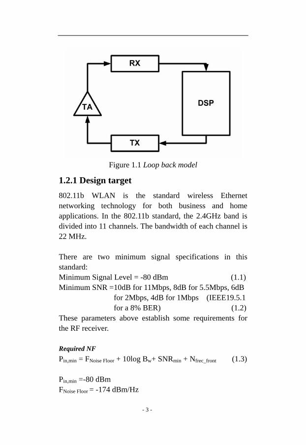
Figure 1.1 Loop back model
1.2.1 Design target 802.11b WLAN is the standard wireless Ethernet networking technology for both business and home applications. In the 802.11b standard, the 2.4GHz band is divided into 11 channels. The bandwidth of each channel is 22 MHz. There are two minimum signal specifications in this standard: Minimum Signal Level = -80 dBm (1.1) Minimum SNR =10dB for 11Mbps, 8dB for 5.5Mbps, 6dB
for 2Mbps, 4dB for 1Mbps (IEEE19.5.1 for a 8% BER) (1.2)
These parameters above establish some requirements for the RF receiver. Required NF Pin,min = FNoise Floor + 10log Bw+ SNRmin + Nfrec_front (1.3)
Pin,min =-80 dBm FNoise Floor = -174 dBm/Hz
- 3 -

Bw =22 MHz SNRmin = 10 dB So we can derive the SSB NF required for the front-end assuming SNR = 10 dB: Nfrec_front = -174 dBm/Hz + 10log(22MHz) + 10 dB
– 80 dBm =10.6 dB (1.4) Required IIP3 To estimate the IIP3, we assume the two adjacent channels 32 dB above the desired channel, due to other available standard specs. Here, the standard assumes 25 MHz channel separation. Hence, the power of the input interferer Pi is –48 dBm. Next, we assume the conversion gain of the front end is G. The SNR of the front-end output is SNRout. The input signal level is Sin. The input interferer level is Pin. We consider the IM3 product corrupting the desired channel as a component of the output noise. This can be shown as in Figure 1.2.
Figure 1.2 Spectrum of the receiver output PIM3 = (Pin+ G)- P = (P∆ in+ G)- 2(IIP3- Pin) =3Pin+ G- 2IIP3 (1.5)
SNRout =( Sin + G)-Nout< (Sin + G) - PIM3 (1.6)
- 4 -

Substituting (1.5) into (1.6), we can get IIP3>( SNRout- Sin+3 Pin)/2=(10+80-3*48)/2=-27 dBm (1.7) But IIP3=-27 dBm is too relaxed. So here at least 6 dB reservation is needed. At last IIP3 should be larger than –21 dBm. In conclusion, the design target of the front end is shown below:
Parameter Value Frequency range 2.4 GHz ~ 2.4835 GHz
Number of channels 11 Channels Bit rate (Rb) 1/2/5.5/11 Mbits/sec Sensitivity -80 dBm
Frame error rate 8% Adjacent Channel rejection 32 dB
NF < 10.6 dB IIP3 > -21 dBm
Table 1.1 Design target of the front end
1.3 Outline of this thesis
Chapter2 introduces some basic background knowledge of RF circuits. Chapter3 introduces several different mixer topologies and compares them by simulation results. Design and simulation of the chosen mixer are presented in detail. Chapter4 shows the integration of the LNA and mixer and the respective simulation results.
- 5 -

In Chapter5 the problem of possible physical defects on the chip is discussed. Short and open defects, likely to occur in the front-end circuit, are simulated and the results are analyzed. In Chapter6 the final conclusions are given.
- 6 -

Chapter 2 RF background
2.1 Nonlinearity
The nonlinear system can be modeled using the following function:
( ) ( ) ( ) ( )21 2 3y t s t s t s tα α α= + + 3 (2.1)
Here is the output and is the input. The
third-order polynomial specifies the third-order nonlinearity. Because of this nonlinearity, distortion is generated. Although there are many measures of nonlinearity, the most commonly used in RF design, are third-order intercept (IP3) and 1-dB compression point.[1]
( )ty ( )tx
2.1.1 Harmonic distortion
Using the function (2.1) with an input
signal ( ) 0cosx t A ω= t , then the function of the output can
be derived as:
( ) 2 2 3 31 0 2 0 3 0
3 32 23 32 2
1 0 0
cos cos cos
3 cos cos 2 cos 32 4 2 4
y t A t A t A t
A AA A0A t t
α ω α ω α ω
α αα αα ω ω⎛ ⎞⎜ ⎟⎜ ⎟
tω⎝ ⎠
= + +
= + + + +
(2.2) Besides the fundamental frequency, which is linear part, the output also includes the harmonic frequency, which is at high frequency and nonlinear. Harmonic distortion is defined as the ratio of the amplitude of a particular harmonic to the amplitude of the fundamental. So the
- 7 -

third-order harmonic distortion ( 3HD ) is the ratio of
amplitude at to the amplitude at : 03ω 0tω
233
1
14
AHD αα
= (2.3)
2.1.2 Intermodulation
Intermodulation appears when the input contains more than one tone. A common used method is “two-tone” test. In this test, the input consists of two tones both of which are strong and at the frequency near the desired band. As a result, these two tones will generate an undesired frequency component in the desired band. [1] For example: Here we assume the input signal is
. Again, by the function (2.1)
the output signal, which has intermodulation distortion, can be expressed as follows:
( ) 1 1 2cos cosx t A t A tω= + 2ω
)
( ) ( ) ( )( )
2
1 1 2 2 1 1 2 2
3
1 1 2 2
1 2
3
cos cos cos cos
cos cos
t A t A t A t A t
A t A t
y ω ω ω ω
ω ω
α αα
= + + +
++ (2.4)
Using trigonometric manipulations, the second-order and third-order intermodulation can be expressed as bellow:
( ) (1 2 2 1 2 1 2 2 1 2 1 2: cos cosA A t A Aω ω α ω ω α ω ω± + + t−
- 8 -

( ) ( )
( ) ( )
2 23 1 2 3 1 2
1 2 1 2 1 2
2 23 2 1 3 2 1
2 1 2 1 2 1
3 32 : 2 24 4
3 32 : 2 24 4
cos cos
cos cos
A A A At t
A A A At t
α αω ω ω ω ω ω
α αω ω ω ω ω ω
± + +
± + +
;
.
−
−
(2.5) The output spectrum is shown in Figure 2.1.
Y(w)
w1-w2
2w1-w2
w1 w2 w0 w1+w21
2w22w1
w
2w2-w1
Reqired filter band width very narrow
Figure 2.1 Output spectrum of two- tone test in frequency
From the spectrum, it can be seen that intermodulation
product at frequency corrupts the desired frequency
. And filtering out the product at is impractical,
because it needs a very narrow band of the filter.
12ω ω− 2
0 2 1ω 2ω ω−
The third-order intermodulation distortion, 3IM , can be
defined as the ratio of the amplitude at frequency
to the amplitude of the fundamental output. By assuming A=A
2 12ω ω−
1=A2, then we get:
- 9 -

3
323
31 1
3344
AA
AIM
α αα α
= = (2.6)
2.1.3 Third-Order intercept Point, IP3
The third-order intercept point is used to measure the intermodulation corruption. Since the desired signal is proportional to A and the third-order product is proportional to , this point is defined as the cross point of these two curves. This is shown in the following Figure 2.2.
3A
Figure 2.2 Graphical representation of the input and output third-order intercept point (IIP3, OIP3) As the power is usually interpreted to decibels, one useful
relation between 3IIP and , is shown as the Equation
(2.7)
3IM
- 10 -

3
3 2dBm
dBm i dBmIMIIP P= − (2.7)
2.1.4 Gain Compression
From (2.2), we notice that at the desired frequency ,
there are two terms due to nonlinearity of the system:
0ω
3
31
3 cos4A
0A tαα⎛ ⎞⎜ ⎟⎜ ⎟
ω⎝ ⎠
+ (2.8)
If is negative, the third order term decreases the gain.
As the input increases, the impact of the third order term becomes more considerable. This phenomenon can be measured by “1 dB Compression Point”. The point is defined as the input level that caused the signal linear gain to drop by 1dB. The definition of 1 dB compression point can be shown in Figure (2.3): [1]
3α
- 11 -

Figure 2.3 1-dB compression point
2.1.5 Cascaded Nonlinear Stages
Figure 2.4 Two cascaded nonlinear stages
The impact of the nonlinearity of each stage on the overall nonlinearity of the whole system can be determined by the following equation:
1 2 11 1 2
3 3,1 3,2 3,3 3,
...1 1 ... n
n
G G GG G GIIP IIP IIP IIP IIP
−≈ + + + + (2.9)
2.2 Noise
The noise is a kind of random signal, which accompanies with the desired signal. The sensitivity of communication system is limited by noise. So it is an important issue, which should be considered in the front-end circuit design. In this section, we will discuss some fundamental noise in the circuits.
- 12 -
2.2.1 Noise source
Thermal Noise Thermal noise is caused by the random thermally generated motion of electrons. It depends on the absolute temperature. The power of thermal noise can be expressed by: [2]
NAP kT f= ∆ (2.10)
Thermal noise occurs in resistive device. In the analysis of the circuits, the spectral density of the noise is preferred. This can be derived from dividing the mean-square noise
value by f∆ .
So the power spectral density (PSD) in figure 2.5 can be given as follows:
2 4ne kTR= ∆f Or
2
22
4 4nn
e kT fiR R
kTG f∆= = = ∆ (2.11)
Shot Noise Shot noise occurs in conducting p-n junctions. The shot noise current depends on the charge of electron, the total DC current flow and the bandwidth. So the PSD of shot noise is given as follows: [2]
2
2 DCi qIf
=∆
(2.12)
Here, is the charge of an electron in coulomb and q DCI
is the value of the dc current in amperes. Flicker Noise Flicker noise or 1/f noise is caused by the
- 13 -

random trapping of charge at the oxide-silicon interface of MOS transistors and in some resistive devices. The PSD can be given as follows: [2]
2DCIi K
f f
α
=∆
(2.13)
Here K and are constant that depend on the nature
of the device.
α
DCI is the current in amperes and f is the
frequency in hertz.
2.2.2 Noise Figure
As noise impacts the performance of the circuits considerably, the parameter called noise figure (NF) is commonly used to specify the additive noise inherent in a circuit or system. This parameter can be used only if the source impedance is resistive. The noise figure is defined as the Equation (2.14):
in in out
out out in
SNR S NNFSNR S N
= = (2.14)
From (2.14), we can see that the noise figure describes how much the SNR degrades after the signal passes through the circuits.
- 14 -

2.2.3 Cascaded Noisy Stage
Figure 2.5 k cascaded stages with noise
The noise figure of overall system is affected by the noise figure of each stage. This can be seen from the following:
321
1 1 2 1 2
11 ......k
k
NF NFNFNF NFG G G G G G −
−−= + + + +1
1− (2.15)
From (2.15), we can see that the noise figure of the whole system is dominated by the first stage if the gain of the following stage is large enough.[1]
2.3 Direct Conversion Receivers
Heterodyne receiver is a common architecture of RF front-end as shown in Figure 2.6
Figure 2.6 Architecture of heterodyne receiver
In this project, however, we choose Direct Conversion architecture shown in Figure2.7
- 15 -
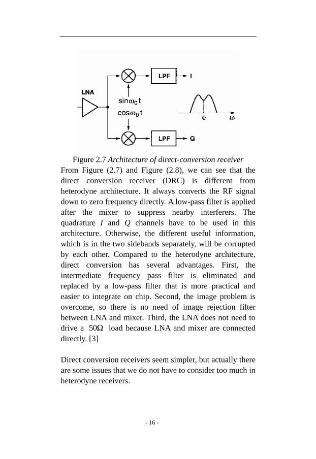
Figure 2.7 Architecture of direct-conversion receiver
From Figure (2.7) and Figure (2.8), we can see that the direct conversion receiver (DRC) is different from heterodyne architecture. It always converts the RF signal down to zero frequency directly. A low-pass filter is applied after the mixer to suppress nearby interferers. The quadrature I and Q channels have to be used in this architecture. Otherwise, the different useful information, which is in the two sidebands separately, will be corrupted by each other. Compared to the heterodyne architecture, direct conversion has several advantages. First, the intermediate frequency pass filter is eliminated and replaced by a low-pass filter that is more practical and easier to integrate on chip. Second, the image problem is overcome, so there is no need of image rejection filter between LNA and mixer. Third, the LNA does not need to drive a load because LNA and mixer are connected directly. [3]
50Ω
Direct conversion receivers seem simpler, but actually there are some issues that we do not have to consider too much in heterodyne receivers.
- 16 -

2.3.1 DC offsets
The DC offsets affect the performance of direct conversion receivers very much. In a DRC, the RF signal is down to zero-IF, so the offsets voltages can corrupt the desired signal. Another impact of DC offsets is that it could saturate the following stage. In the RF front-end, the isolation between the LO port and the input port of the LNA and the mixer is not perfect. So the feedthrough occurs between the LO port and the input port of the LNA and the mixer. This is called “LO leakage”, which results from capacitive and substrate coupling. As the LO signal leaks to the inputs of the LNA and the mixer, it is mixed with the desired LO signal. As a result, the DC voltage appears at the output of low-pass filter. This phenomenon is called “self-mixing”. When a strong interferer leaks from the input of the LNA or the mixer to the LO port, a similar phenomenon occurs as well. When the LO signal leaks to the antenna and radiate, the problem of offsets is exacerbated. In this case, the leakage signal will be reflected from moving objects. This means that the DC offsets is time varying and difficult to separate from the actual signal.[3]
- 17 -

Figure 2.8 (a) “self mixing” of LO (b) “self mixing” of
interferer
2.3.2 I/Q Mismatch
As shown in figure 2.8 of DCR, there are quadrature I and Q channels in a DRC. So either the RF signal or the LO signal should be shifted by 90o. Since shifting the RF signal involves severe noise-power-gain tradeoffs, we often choose LO signal for shifting. In either case, the phase or amplitude errors, which occur in I and Q signals, corrupt the down converted signal constellation. Therefore the bit error rate will rise.[3]
2.3.3 Even-Order Distortion
Besides the odd-order distortion, the even-order distortion also appears as a problem. For two-tone test, as we
- 18 -

illustrate in (2.5), there is a product of second
order: (2 1 2 1 2cos )A Aα ω − tω
)
. In an ideal mixer, there is no
direct feedthrough from the RF port to the IF port. But actually, there is some feedthrough here. Hence, the RF signal appears at the output without frequency conversion.
In this case, the low-frequency beat signal could
be observed at the output and corrupts the desired signal as well.
( 1 2ω ω−
Second-order distortion can be characterized by the point “second intercept point”, IP2, which is defined as the cross point of the input power and the second-order signal power plots. [3]
2.3.4 Flicker Noise
Since the down converted signal is around zero frequency, the 1/f noise affects the performance of the front-end according (2.13).
- 19 -

Chapter 3 Mixers In the RF receivers, the function of a mixer is to convert a RF signal to a lower frequency, called intermediate frequency (IF). The principle of a mixer is based on using a multiplication between the RF signal and LO signal in the time domain to get the desired signal. This principle can be shown by the following trigonometric identity:
( )( ) ( ) ( )1 2 1 2 1cos cos cos cos2
AB2A t B t t tω ω ω ω ω ω= + + −⎡ ⎤⎣ ⎦
(3.1) From (3.1) we see that there is the product of difference
frequency (ω1-ω2) at the mixer output. The amplitude of the
product is proportional to the amplitude of the RF and the LO signals. The amplitude of the LO signal is constant so that the amplitude of IF is transferred from the amplitude of RF signal. [1] Conversion Gain The conversion gain (Gc ) is defined as the ratio of the amplitude of the IF signal to the amplitude of the RF signal. Generally, Gc should be large so that distortion and noise could be low. Noise Figure It is the signal-to-noise ratio (SNR) at the RF port divided by the SNR at the IF port. The typical values for SSB (single side band) NF range from 10dB to 15dB. If the gain of the LNA is large enough, from (2.7) we can know that the overall receiver NF will be dominated by the NF of the LNA and not by the mixer. Generally, the single-sideband noise figure (SSB) is preferred for describing the quality of the mixer. But in a DCR (direct downconversion receiver), the double-sideband noise figure
- 20 -

is of interest, because both sidebands of the RF signal contain useful information. The DSB value is 3dB lower than the SSB if the conversion gains of the two sidebands are the same. Linearity As any amplitude modulation in the RF signal is transferred to the IF signal, it requires a good linearity of the mixer. Usually, IIP3 is used to measure the linearity of the mixer. But in a DRC, IIP2, which characterizes the second-order distortion, should be considered as well.
3.1 CMOS RF Mixer Topologies
Mixers can be classified as active and passive mixers. The major factor used to distinguish them is the conversion gain (Gc). For the active mixers, the conversion gain is usually larger than 1, while it is always less than 1 for the passive mixers. On the other hand, the distortion performance of the active mixers is worse than of the passive mixers. So there is a trade-off at distortion vs. gain, which exists between the passive and active mixers.
3.1.1 Single Balanced Active Mixer
The basic structure of single balanced mixer is shown in Figure 3.1. The transistor MRF always works in the saturation region. As shown, the RF signal is applied at the gate of the MRF so that it is converted to a current signal. The DC voltage of transistors MLO+ and MLO- are set around the threshold level.
- 21 -

As the LO signal is applied, MLO+ and MLO- will switch on and off in turn. While one of the LO transistor is on, the other is off. This requires the LO signal large enough to drive the completing switch. In this case, the RF signal is multiplied by the LO signal. If we assume the LO signal is an ideal square wave, then the IF signal can be expressed as following:
( ) cosif rf rfV t A tω= *0
1
sin22 cos
2n
n
G n
π
ωπ∞
=∑ n t (3.2)
The advantage of this structure is the rejection of RF feedthrough. As the IF signal is taken from both branches and follows the load resistors, the IF signal is derived from the difference of the two branches. So the RF feedthrough from both branches can cancel each other. On the other hand, the feedthrough of the LO signal will appear at the output. [1]
Figure 3.1 Single balanced active mixer
- 22 -

The conversion gain of active mixer is proportional to the gm of the RF transistor. So a large gm can increase the conversion gain of the mixer. And it could decrease the thermal noise as well. From the Figure 3.2 and Figure 3.3, we can see that when the size of the RF transistor increases to 200 um, it can achieve a lower NF and larger conversion gain. To perform a better switching activity, the size of the LO signal should be also very large. Here the LO transistors are sized at 200 um.
20
21
22
23
24
25
26
0 5 10 15 20 25
N u mb e r o f g a t e s
Figure 3.2 NF vs. Size of the RF transistor
- 23 -
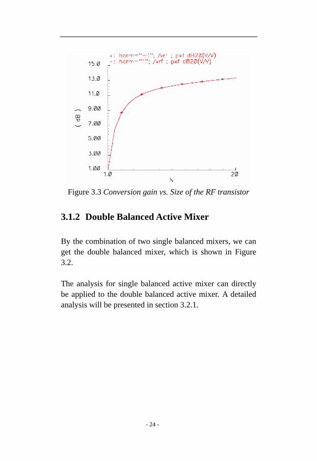
Figure 3.3 Conversion gain vs. Size of the RF transistor
3.1.2 Double Balanced Active Mixer
By the combination of two single balanced mixers, we can get the double balanced mixer, which is shown in Figure 3.2. The analysis for single balanced active mixer can directly be applied to the double balanced active mixer. A detailed analysis will be presented in section 3.2.1.
- 24 -

Figure 3.4 Double balanced active mixer
The nonlinearity and noise performance of the double balanced mixer are better compared to the single balanced mixer. But it consumes larger current than the single balanced mixer. Compared to the single balanced mixer, the double balanced mixer can cancel the feedthrough of both the LO and the RF signal. But this only happens under ideal conditions. Actually, the mismatches at the RF or the LO port will cause some feedthrough.
3.1.3 Single-ended Sampling Mixer
The unbalanced sampling mixer is a kind of passive mixer, the structure of which is shown as the Figure 3.5.
- 25 -
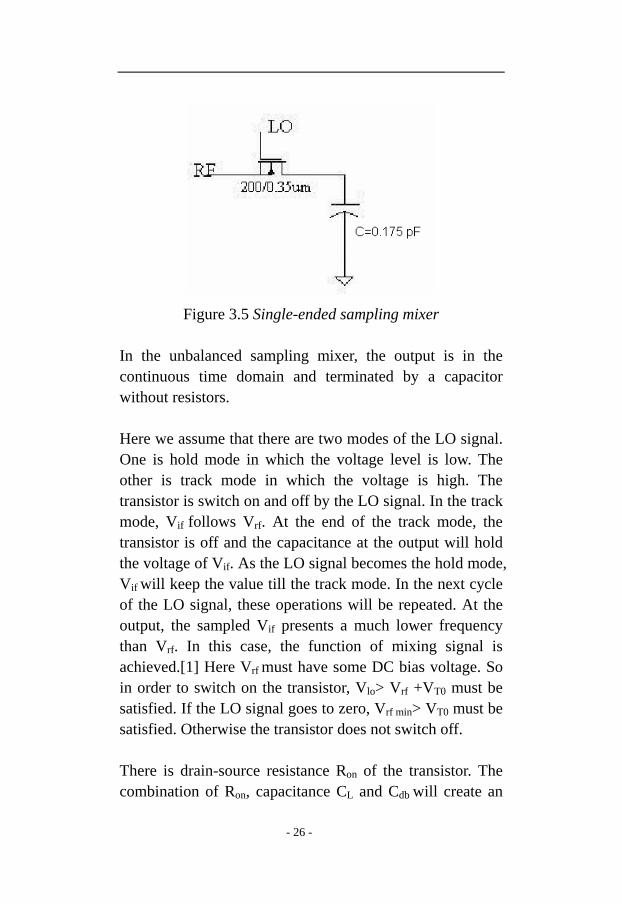
Figure 3.5 Single-ended sampling mixer
In the unbalanced sampling mixer, the output is in the continuous time domain and terminated by a capacitor without resistors. Here we assume that there are two modes of the LO signal. One is hold mode in which the voltage level is low. The other is track mode in which the voltage is high. The transistor is switch on and off by the LO signal. In the track mode, Vif follows Vrf. At the end of the track mode, the transistor is off and the capacitance at the output will hold the voltage of Vif. As the LO signal becomes the hold mode, Vif will keep the value till the track mode. In the next cycle of the LO signal, these operations will be repeated. At the output, the sampled Vif presents a much lower frequency than Vrf. In this case, the function of mixing signal is achieved.[1] Here Vrf must have some DC bias voltage. So in order to switch on the transistor, Vlo> Vrf +VT0 must be satisfied. If the LO signal goes to zero, Vrf min> VT0 must be satisfied. Otherwise the transistor does not switch off. There is drain-source resistance Ron of the transistor. The combination of Ron, capacitance CL and Cdb will create an
- 26 -

R-C network. This will introduce some delay. So the Vif cannot follow Vrf perfectly. In this case, the distortion occurs during mixing. The noise figure of the sampling mixer can be expressed by the following equation:
(3.2)
From (3.2), we can see that the NF decreases by increasing the frequency of LO. And to obtain low noise figure, the load capacitance of the mixer should be large enough. But the hold capacitance is constraint by the sampling accuracy that affects mixer gain and linearity. [8] Here we assume Ton=(Rsw+RLNA) CL. To assure accuracy of sampling, we get the condition of Ton: [8]
⎟⎟⎠
⎞⎜⎜⎝
⎛≤
sff 121;
21MinTon
RFπ (3.3)
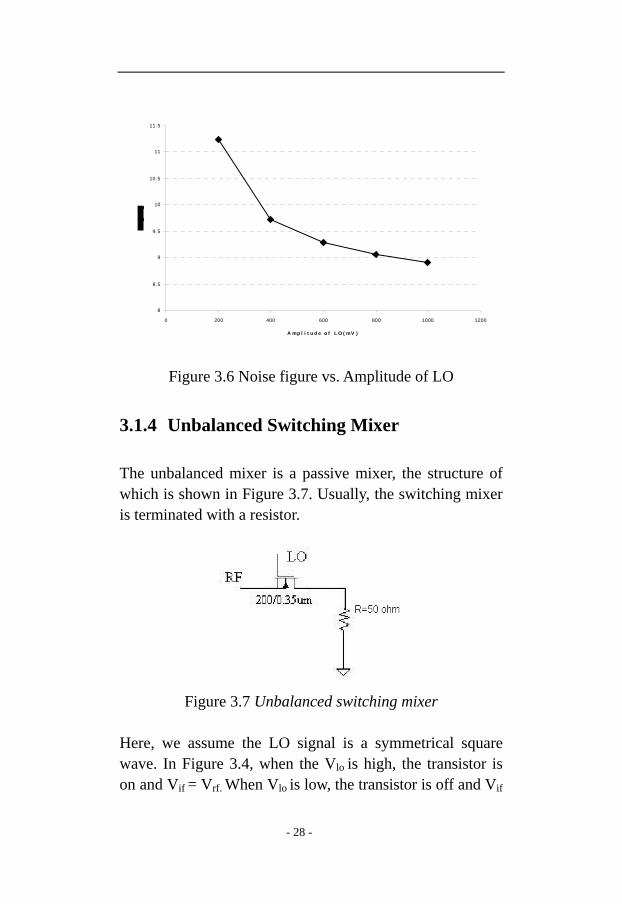
For fRF=fs=2.4G Hz, we get Ton ≤ 35 ps. Hence for a typical value Rsw+RLNA ≈ 100-200 ohms we have CL ≤ 0.175 pF. In order to get low noise figure(3.3), the value of CL should be maximized. So CL=175 pF. The amplitude of the LO signal should be decided for the better performance. This optimum value is given from the simulation for different LO amplitudes. But the conversion gain of passive mixer is independent of the LO signal. Hence, only the NF is simulated by varying the amplitude of the LO. The simulation result is shown in Figure 3.6. The NF drops down as the amplitude of the LO increases. But too large amplitude of LO will consume a lot of power. So here 1 V is chosen as the amplitude of the LO.
- 27 -
8
8.5
9
9.5
10
10.5
11
11.5
0 200 400 600 800 1000 1200
A mp l i t u d e o f L O ( mV )
Figure 3.6 Noise figure vs. Amplitude of LO
3.1.4 Unbalanced Switching Mixer
The unbalanced mixer is a passive mixer, the structure of which is shown in Figure 3.7. Usually, the switching mixer is terminated with a resistor.
Figure 3.7 Unbalanced switching mixer
Here, we assume the LO signal is a symmetrical square wave. In Figure 3.4, when the Vlo is high, the transistor is on and Vif = Vrf. When Vlo is low, the transistor is off and Vif
- 28 -

=0. In this case, the output is the product of multiplication between the RF and the LO signal. The RF signal is
( ) cosrf rf rfV t A tω= (3.4)
The mixer input signal can be represented by its equivalent Fourier series as follows:
( ) (1
sin1 2 cos2
2
lo lon
n
V t n tn
π
ωπ∞
=
= + ∑ ) (3.5)
The output signal is
( ) ( ) ( )
( )1
sin1 2cos cos2
2
if rf lo
rf rf lon
V t V t V t
n
A t nn
π
ω ωπ∞
=
=
t
⎛ ⎞⎜ ⎟
= +⎜ ⎟⎜ ⎟⎝ ⎠
∑ (3.6)
With a band pass filter, we can get the IF signal at
frequency . The IF signal can be written as (3.7) rf loω ω−
( ) (1 cosif rf rf loV t A tω ωπ
= − ) (3.7)
According the definition of , for the unbalanced mixer
we obtain:
cG
1
cGπ
= (3.8)
Which is smaller than 1. [1] The noise figure of unbalanced mixer depends on the Ron, which is the on resistance of the transistor. (NF-1) ~ Ron (3.9)
- 29 -

The conversion gain is related to the Ron as well:
Gc ~ RR
R
on + (3.10)
From (3.9) and (3.19), we can see that the size of the transistor should be large to obtain small Ron. Then we can get the low noise figure and large conversion gain. To obtain the optimum size of the transistor, the NF is simulated by changing the size of the transistor. As shown in the result of Figure 3.8, the noise figure can achieve the lowest value when the transistor size is 200um. But as the size of the transistor increases, the parasitic capacitance of the transistor will increase as well. Then the feed through will be more serious, especially between the LO and the IF output. As a result it will degrade the performance of the mixer. So the size of the transistor is limited by the parasitic effect. The amplitude of the LO signal is 1 V which is optimized in the similar way as in the single ended sampling mixer.
0
5
10
15
20
25
0 5 10 15 20 25
Number of gates
NF(
dB)
Figure 3.8 NF vs. size of the transistor
- 30 -
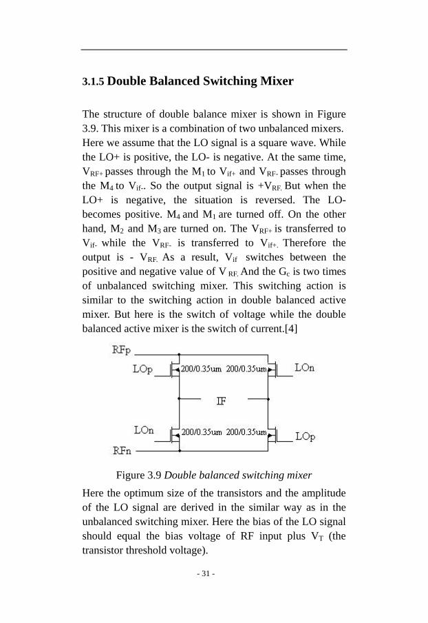
3.1.5 Double Balanced Switching Mixer
The structure of double balance mixer is shown in Figure 3.9. This mixer is a combination of two unbalanced mixers. Here we assume that the LO signal is a square wave. While the LO+ is positive, the LO- is negative. At the same time, VRF+ passes through the M1 to Vif+ and VRF- passes through the M4 to Vif-. So the output signal is +VRF. But when the LO+ is negative, the situation is reversed. The LO- becomes positive. M4 and M1 are turned off. On the other hand, M2 and M3 are turned on. The VRF+ is transferred to Vif- while the VRF- is transferred to Vif+. Therefore the output is - VRF. As a result, Vif switches between the positive and negative value of V RF. And the Gc is two times of unbalanced switching mixer. This switching action is similar to the switching action in double balanced active mixer. But here is the switch of voltage while the double balanced active mixer is the switch of current.[4]
Figure 3.9 Double balanced switching mixer
Here the optimum size of the transistors and the amplitude of the LO signal are derived in the similar way as in the unbalanced switching mixer. Here the bias of the LO signal should equal the bias voltage of RF input plus VT (the transistor threshold voltage).
- 31 -

3.1.5 Simulation results and Analysis
All these mixers we have discussed here were designed in
0.35µm standard CMOS technology and verified using
Spectre RF simulator in Cadence environment. The results presented below are based on the circuit level simulation of the mixers. Table 3.1 gives a comparison of simulation results for the all designed mixer. In order to compare the performance of the different mixer topologies, both of the LO and the RF signals in all the mixers are set to 2.4GHz. The Vpp of the LO signal in the active mixers is 300mV while it is 2V in the passive mixers. The noise figure here we measured is an average value from 1MHz to 23MHz. (The value is based on the 802.11b standard.) Apparently, compared to the passive mixers, active mixers have some advantages and disadvantages: Advantages: 1) The conversion gain is much larger than the passive mixers. 2) The amplitude of LO signal needed is much lower than the passive mixers. In practice, if the amplitude of the high frequency sinusoidal or square wave is lower, the LO is much easier to implement. Disadvantages: 1) The NF is larger than of the passive mixers. 2) The linearity is worse compared to the passive mixers. 3) They need DC power supply.
- 32 -
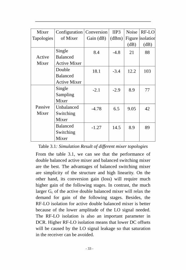
Mixer Tapologies
Configuration of Mixer
Conversion Gain (dB)
IIP3 (dBm)
Noise Figure (dB)
RF-LO isolation
(dB) Single Balanced Active Mixer
8.4 -4.8 21 88 Active Mixer
Double Balanced Active Mixer
18.1 -3.4 12.2 103
Single Sampling Mixer
-2.1 -2.9 8.9 77
Unbalanced Switching Mixer
-4.78 6.5 9.05 42
Passive Mixer
Balanced Switching Mixer
-1.27 14.5 8.9 89
Table 3.1: Simulation Result of different mixer topologies From the table 3.1, we can see that the performance of double balanced active mixer and balanced switching mixer are the best. The advantages of balanced switching mixer are simplicity of the structure and high linearity. On the other hand, its conversion gain (loss) will require much higher gain of the following stages. In contrast, the much larger Gc of the active double balanced mixer will relax the demand for gain of the following stages. Besides, the RF-LO isolation for active double balanced mixer is better because of the lower amplitude of the LO signal needed. The RF-LO isolation is also an important parameter in DCR. Higher RF-LO isolation means that lower DC offsets will be caused by the LO signal leakage so that saturation in the receiver can be avoided.
- 33 -

3.2 Mixer Design
3.2.1 Design Requirements
Parameter Value RF frequency 2.4 GHz LO frequency 2.4 GHz IF frequency 0 Hz
Conversion Gain > 10 dB DSB NF 7 dB ~ 12 dB
IIP3 > -10 dBm IIP2 >10 dBm
RF- to- LO isolation Around 100 dB Table 3.2 Design requirement of the mixer
- 34 -

3.2.2 Circuit design
Figure 3.10 Double balanced active mixer
As the discussion in section 3.1.5, the double balanced active mixer has largest conversion gain, good linearity and RF-to-LO isolation around 100dB. The noise figure is also acceptable. So the double balanced active mixer is chosen to implement in RF front end. The differential structure is used to suppress the LO and the RF signal feed through. And in this way, the linearity and conversion gain are also improved. The schematic of the mixer is shown in Figure 3.10. For a standard double balanced active mixer, both of M2 and M3 should be driven by the RF signal. But here the designed LNA is single ended. We have tried to use a balun to transfer the single ended signal to a differential signal.
- 35 -

Although the balun can function, it degrades the performance of the front end much. In this case, we only apply a DC bias voltage to the gate of M2. Just M3 is driven by the RF signal. M1 is a bias transistor whose input is from the mirror current. Now, because of the unbalanced RF input, the linearity and conversion gain of the mixer will be degraded. But it is still acceptable. The LO stage contains four transistors M4-M7. M4 and M7 are driven by the same LO signal as M5 and M6 but shifted 180o in phase. M4-M7 are sized very wide, 200um. In this case, large current can be obtained. And the switching operation of the transistors will be better. The DC voltages of M4-M7 are biased close to their threshold in order to make a good switching on and off. The RF transistors are sized very large as well, 200 um. So it could provide a large gm to increase the Gc and a to lower thermal noise. We got the curve of conversion gain and NF varying by changing the width of the RF transistor. It is shown in Figure 3.11. From the figure we can see that the mixer can get good enough performance for 200um width of the RF transistors.
- 36 -

Figure 3.11 Gc and NF vs. size of the RF transistors
The DC bias current also affects the performance of the mixer. By sweeping the DC bias current, we can see that NF varies. The curve of this variation can be seen from Figure 3.12. From this figure we can see that when the current increases from 1mA to 2mA, the NF decreases quite fast. However, the bias transistor cannot work in saturation region (that is the required region for its function) for large value of the current. So here we choose 2.6mA for the DC bias current.
- 37 -

Figure 3.12 NF vs. bias current
The IF signal is a differential output. Both branches are connected with common drain buffers with high input resistance and its gain is almost 1. The amplitude of the LO signal should be decided for the better performance. This optimum value is given from the simulation for different LO amplitudes. The simulation result is shown in Figure 3.13.
- 38 -

Figure 3.13 Conv.Gain & NF of the double balanced active
mixer
3.2.3 Simulations
In the simulation, both of the LO signal and the RF signal are at 2.4 GHz. In 802.11b WLAN, each channel is 22 MHz and contains no subcarriers. So here the noise figure we measured is an average value from 1 MHz to 23 MHz of double-sideband noise figure (DSB).
- 39 -

Figure 3.14 IIP3 curve of the double balanced active mixer
Figure 3.15 SSB noise figure of the double balanced mixer
From Figure 3.15, we can see that when the frequency is
- 40 -

close to zero, the noise figure becomes much higher. This phenomenon is caused by the 1/f noise, which dominates the noise as the frequency decreases to zero. The noise effect of the whole channel can be derived by calculating the average value of the noise figure in the channel frequency range. Here the range is from 1 MHz to 23 MHz derived by the 802.11b WLAN standard.
Figure 3.16 Conversion gain of double balanced active
mixer
3.2.4 The Layout of Mixer
The performance of the active double balanced mixer is sensitive to any unbalance of the circuit. So in the layout, it should be as symmetrical as possible. Because the active double balanced mixer is composed of two active single balanced mixers. We can draw the layout of one single balanced mixer at first. Then make a copy of it and side the
- 41 -

copy away. In this way, the layout could get a better symmetry. The layout of the mixer is shown in Figure 3.17.
Figure 3.17 Layout of the double balanced active mixer
3.2.5 Mixer Performance Summary
In the table 3.3, the simulation result of both layout and schematic of the mixer is shown.
Schematic of the mixer
Layout of the mixer
Power supply (V) 3.3 3.3 Average DSB NF
(dB) 9.9 10.2
Conversion gain (dB)
17.4 16.2
IIP3 (dBm) -2.8 -2.4 IIP2 (dBm) 32.3 34.7
RF-LO isolation (dB)
102 103
Table 3.3 Performance of the mixer
- 42 -

Chapter 4 Front End Integration The front-end which is designed for look back BIST design based on the 802.11b WLAN. The direct conversion receiver (DCR) is selected whose architecture is shown in figure 2.7. The performance of the LNA is shown in Table 4.1
Parameter Value Power Supply 3.3V Voltage Gain 14.5 dB
S11 <-10 dB NF 3.6 dB IIP3 -15 dBV Table 4.1 Performance of the LNA
The performance of the RF front-end is shown in Table 3.3.
Schematic of the front-end
Layout of the front-end
Average SSB NF (dB)
8.9 9.7
Conversion gain (dB)
24.9 22
IIP3 (dBm) -11.4 -10.4 Table 3.3 Simulation result of the front-end
- 43 -

Chapter 5 RF Front-end Circuits with Defects
Our design aims at RF testability. In this chapter we focus on the spot defects in RF blocks typical of CMOS technology. Here, we introduce open or short defects into the front end. Each time only one defect is introduced into the circuits. By the values of NF and conversion gain, we can see how these defects can degrade the performance of the front end. [6]
5.1 Short Defects
A typical matching resistance, Rs=50ohm, is assumed as a reference here. We define the respective spot fault as a short resistance Rsh. between two nodes, such as between drain-gate or source-gate in a transistor (defects in gate oxide). Alternatively, the short defects can occur between two close signal paths due to process imperfections (e.g. remaining after polishing small pieces of metal).
5.1.1 Short Defects in LNA
The short resistance Rsh is introduce between two points of layout. These points are indicated in Figure 5.1.
- 44 -
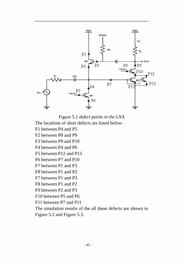
Figure 5.1 defect points in the LNA
The locations of short defects are listed below: F1 between P4 and P5 F2 between P8 and P9 F3 between P9 and P10 F4 between P4 and P6 F5 between P12 and P13 F6 between P7 and P10 F7 between P1 and P3 F8 between P1 and P2 F7 between P1 and P3 F8 between P1 and P2 F9 between P2 and P3 F10 between P5 and P6 F11 between P7 and P11 The simulation results of the all these defects are shown in Figure 5.2 and Figure 5.3.
- 45 -
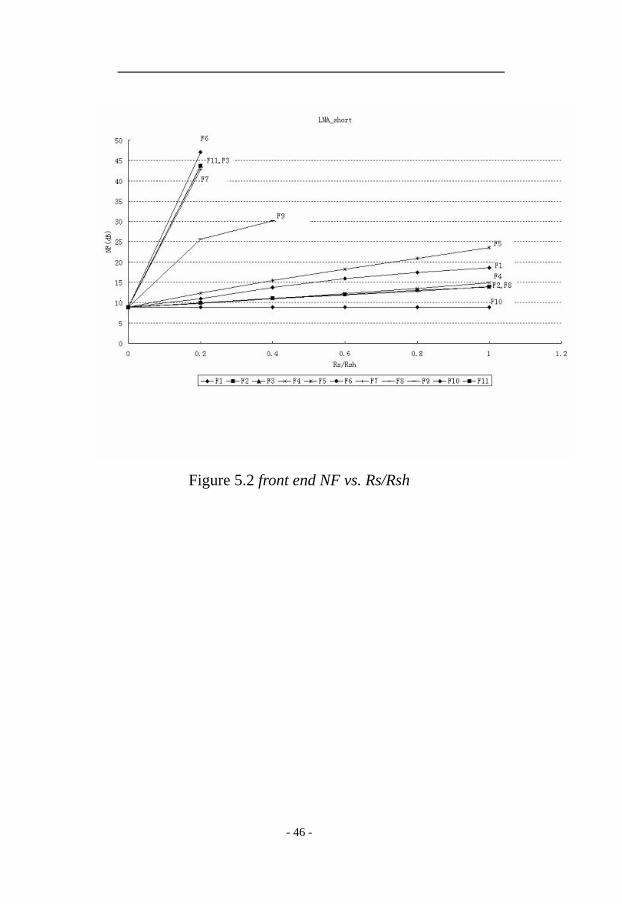
Figure 5.2 front end NF vs. Rs/Rsh
- 46 -

Figure 5.3 Front end Conv.Gain vs. Rs/Rsh
From the figures, we can see that: F1, F3, F5, F6, F7, F9 and F11 degrade the performance of the front end obviously. With these defects the circuits cannot work any more, but with F2, F4, F8, F10 the performance of the circuits will not be degraded too much. Since we want to see a more pronounced effect of these defects, we decrease Rsh to 1 Ohm to make the defects stronger. The result is shown in Table 5.1. NF (dB) Conv.Gain(dB) F2 42.7 -12.9 F4 77.4 -47.1 F8 59.3 -29.5 F10 8.9 24.9
Table 5.1 Simulation results with Rsh =1 ohm
- 47 -
5.1.2 Short Defects in Mixer
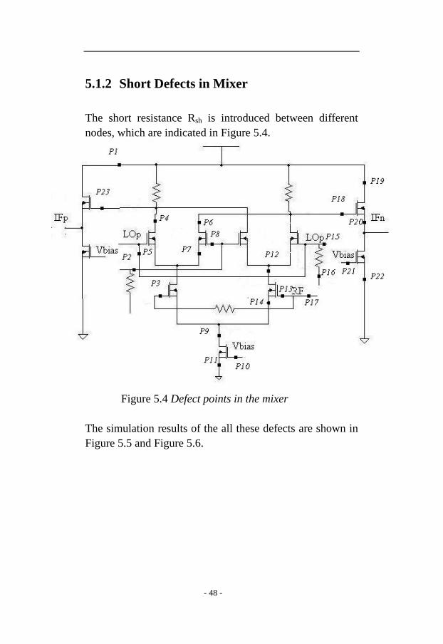
The short resistance Rsh is introduced between different nodes, which are indicated in Figure 5.4.
Figure 5.4 Defect points in the mixer
The simulation results of the all these defects are shown in Figure 5.5 and Figure 5.6.
- 48 -

Figure 5.5 Front end Conv.Gain vs. Rs/Rsh
Figure 5.6 Front end NF vs. Rs/Rsh The locations of the short defects in the mixer are listed
- 49 -

below: F1 between P12 and P14 F2 between P18 and P19 F3 between P12 and P13 F4 between P6 and P7 F5 between P19 and P20 F6 between P9 and P10 F7 between P9 and P11 F8 between P1 and P4 F9 between P20 and P22 F10 between P15 and P23 F11 between P22 and P23 F12 between P2 and P3 F13 between P5 and P8 F14 between P16 and P20 F15 between P17 and P20 F16 between P1 and P18 F3, F4, F5, F6 and F11 degrade the performance of the circuits very obviously. With these defects, the mixer cannot work because F3, F4, F5, F6 and F11 degrade the performance too much. For more accuracy we appropriately change the scale of Y-axis. Then Figure 5.5 and 5.6 can be redrawn resulting in Figure 5.7 and Figure 5.8.
- 50 -

Figure 5.7 Front end NF vs. Rs/Rsh
Figure 5.8 Front end Conv.Gain vs. Rs/Rsh We can see that:
- 51 -

Actually, F1, F7 and F12 have a significant impact the performance of the circuits as well. For F1, the source and the drain of the RF transistor are connected by Rsh and as a result, the input RF signal is corrupted seriously by this defect. So the circuits cannot function. For F7, the drain of the current source transistor is shorted to ground, so the DC operating point is changed. As a result, the RF or the LO transistors can work in the correct region, but F7 will affect the function of the circuit when stronger than 0.4. F12 seems like a serious LO leakage to the RF port. In this case, the self-mixing will occur. So it corrupts the desired signal much. But others are still not very obviously. So we increase the strength of the short defects by decreasing Rsh to 1 ohm. The result is: F13 NF=41.8 dB Gc=-11.77 dB F15 NF=23.9 dB Gc=5.4 dB F13 and F15 have obvious effects on the circuits. But F2, F8, F9, F10, F14 and F16 almost keep the same value of NF and Gc as 50ohm short defect. In F9, the drain of the bias transistor in the buffer is shorted to ground. This defect will change the DC operating point of the output buffer. But it will not impact the amplifier transistor of the buffer seriously. So IF output is almost the same as before. In F10, it seems like a LO leakage to the IF output. But the IF signal is around 0 Hz while the LO signal is 2.4 GHz whose frequency is much higher. The LO signal is out of band. So the simulation result will not impact by this out band signal. In F8, it seems like one branch of the mixer without load resistance. So this will not impact the NF and conversion gain of the mixer apparently.
- 52 -
5.2 Open Defects
Also in this case, Rs=50ohm matching resistance is assumed the reference. Here we define the spot fault as an open resistance Ro. The open defects can be anywhere in the circuits. Usually, they occur due to resistive vias, resistive contacts or cracks in signal paths.
5.2.1 Open Defects in LNA
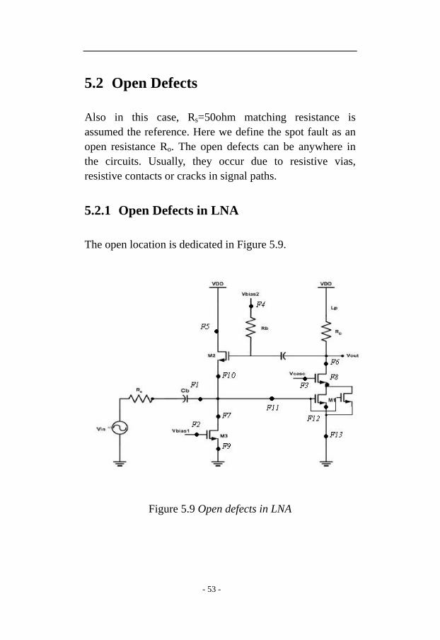
The open location is dedicated in Figure 5.9.
Figure 5.9 Open defects in LNA
- 53 -

Figure 5.10 Front end Conv.Gain (dB) vs. Ro/Rs
- 54 -

Figure 5.11 Front end NF (dB) vs. Ro/Rs
From Figure 5.10 and Figure 5.11, we can see that F1, F6, F8, F10, F11, F12 have very obvious impact on the circuits. In F6, F8 and F11, the amplifier transistor of the LNA cannot work. In this case, the LNA cannot function. In F10, the transistor for input matching does not have function anymore. So this will degrades the performance obviously. But other defects do not have enough impact to see. So we increase the strength of these open defects. The largest value of Ro increases to 10K ohm. The simulation result can be seen from Figure 5.12 and Figure 5.13. In F5 and F9, the apparent degradation can be seen. But F2, F4, F3, F7 and F13 still do not have much obvious effects. So we introduce totally open defects in these locations. The result is shown in table 5.2.
- 55 -

Figure 5.12 Front end Conv.Gain (dB) vs. Ro (ohm)
Figure 5.13 Front end NF (dB) vs. Ro(ohm)
- 56 -
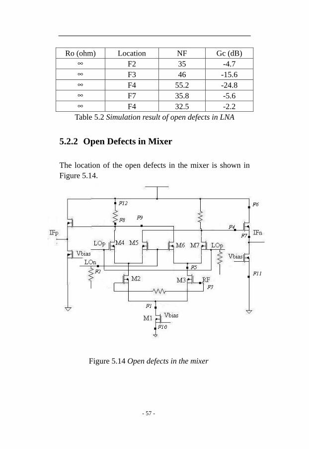
Ro (ohm) Location NF Gc (dB) ∞ F2 35 -4.7 ∞ F3 46 -15.6 ∞ F4 55.2 -24.8 ∞ F7 35.8 -5.6 ∞ F4 32.5 -2.2
Table 5.2 Simulation result of open defects in LNA
5.2.2 Open Defects in Mixer
The location of the open defects in the mixer is shown in Figure 5.14.
Figure 5.14 Open defects in the mixer
- 57 -

Figure 5.15 Front end Conv.Gain (dB) vs. Ro/Rs
Figure 5.16 Front end NF (dB) vs. Ro/Rs
- 58 -
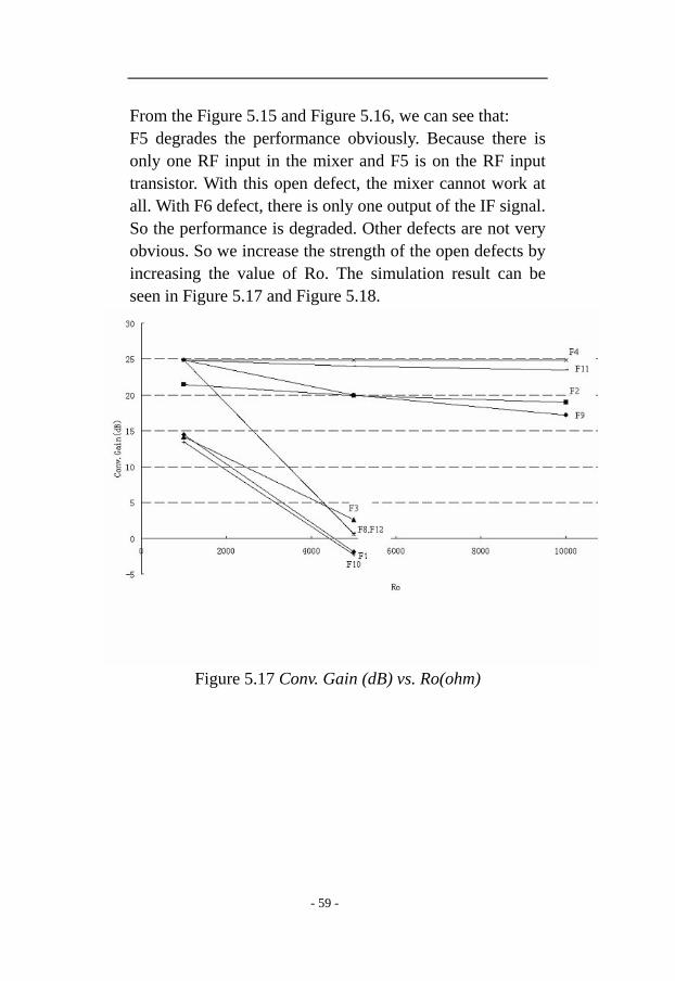
From the Figure 5.15 and Figure 5.16, we can see that: F5 degrades the performance obviously. Because there is only one RF input in the mixer and F5 is on the RF input transistor. With this open defect, the mixer cannot work at all. With F6 defect, there is only one output of the IF signal. So the performance is degraded. Other defects are not very obvious. So we increase the strength of the open defects by increasing the value of Ro. The simulation result can be seen in Figure 5.17 and Figure 5.18.
Figure 5.17 Conv. Gain (dB) vs. Ro(ohm)
- 59 -

Figure 5.18 Front end NF (dB) vs. Ro (ohm)
From Figure 5.17 and Figure 5.18, we can see that: F1 and F10 become more obvious. Because the DC operating point of the circuit will be changed with very large resistance. The circuit cannot function. F3 becomes more obvious. With a lower resistance, it looks like a load resistance added to the RF port. So it is not very obvious. But with very large resistance, it is almost an open to the RF input. The circuit cannot work. F8 and F12 become more obvious. Because with lower resistance, this defect just affect the balance of the circuit. With larger resistance, one of the two branches in the mixer cannot work. F2, F4, F9, F11 are still not very obvious. So we introduce totally open in these locations. Then we get the result in table 5.3.
- 60 -

Ro Location NF (dB) Gc (dB) ∞ F2 44.75 1.87 ∞ F4 10.5 18.9 ∞ F9 17.6 17.4 ∞ F11 10.35 19.13
Table 5.3 Simulation result with open defect in the mixer
- 61 -

Chapter 6 Conclusion The RF receiver front-end using 0.35um CMOS technology has been designed based on the 802.11b standard WLAN. The direct downconversion architecture was used for the receiver. This thesis work was focused on the mixer design. Five different topologies of mixers have been designed using 0.35um CMOS technology and simulated on the schematic level. Finally, the active double balanced mixer was chosen to be implemented in the RF front end. Both of the schematic and the layout of the mixer were simulated. Due to the simulation results the mixer can achieve conversion gain of 16.2 dB, DSB noise figure lower than 12 dB and IIP3 of –2.8 dB. It shows that the mixer can satisfy the design requirements. After integration with the available LNA, the simulation results have shown that this front-end can achieve a conversion gain of 22 dB, SSB noise figure less than 10.6 dB and IIP3 of –10.4 dBm that much larger than the required IP3. In effect, the assumed design specification are fully met. The extension of this work is RF front-end design for testability. For this reasons the RF front end has also been simulated for short and open defects, typical of CMOS technology. An impact of those defects on the performance of the font end has been analyzed. In the future, when testing the fabricated chip the possible defects can be estimated by contrasting the chip output and the simulation results we have done here.
- 62 -

References [1] Bosco Leung, VLSI for Wireless Communication, Prentice Hall, 2002 [2] Thomas H. Lee, The Design of CMOS Radio-Frequency Integrated Circuits, 2nd Edition, Cambridge University Press, 2004 [3] Behzad Razavi, Design Considerations for Direct-Conversion Receivers, IEEE Transactions on Circuits And Systems-II: Analog And Digital Signal Processing, Vol. 44, NO. 6, June 1997 [4] Arif A. Siddiqi, 2.4 GHz RF Down-Conversion Mixers in Standard CMOS Technology, ISCAS 2004 [5] Jacob Pihl, Direct Downconverison With Switching CMOS Mixer, IEEE 2001 [6] Jerzy Dabrowski, Fault Modeling of RF Blocks Based on Noise Analysis, ISCAS 2004 [7] Jerzy Dabrowski, BiST Model for IC RF-Transceiver Front-End, Proceedings of 18th IEEE International Symposium on Defect and Fault Tolerance in VLSI Systems (DFT’03) [8] Darius Jakonis, Jerzy Dabrowski, Christer Svensson, Noise Analysis of Downconversion Sampling Mixer, ECCTD 2003
- 63 -

På svenska Detta dokument hålls tillgängligt på Internet – eller dess framtida ersättare – under en längre tid från publiceringsdatum under förutsättning att inga extra-ordinära omständigheter uppstår.
Tillgång till dokumentet innebär tillstånd för var och en att läsa, ladda ner, skriva ut enstaka kopior för enskilt bruk och att använda det oförändrat för ickekommersiell forskning och för undervisning. Överföring av upphovsrätten vid en senare tidpunkt kan inte upphäva detta tillstånd. All annan användning av dokumentet kräver upphovsmannens medgivande. För att garantera äktheten, säkerheten och tillgängligheten finns det lösningar av teknisk och administrativ art.
Upphovsmannens ideella rätt innefattar rätt att bli nämnd som upphovsman i den omfattning som god sed kräver vid användning av dokumentet på ovan beskrivna sätt samt skydd mot att dokumentet ändras eller presenteras i sådan form eller i sådant sammanhang som är kränkande för upphovsmannens litterära eller konstnärliga anseende eller egenart.
För ytterligare information om Linköping University Electronic Press se förlagets hemsida http://www.ep.liu.se/ In English The publishers will keep this document online on the Internet - or its possible replacement - for a considerable time from the date of publication barring exceptional circumstances.
The online availability of the document implies a permanent permission for anyone to read, to download, to print out single copies for your own use and to use it unchanged for any non-commercial research and educational purpose. Subsequent transfers of copyright cannot revoke this permission. All other uses of the document are conditional on the consent of the copyright owner. The publisher has taken technical and administrative measures to assure authenticity, security and accessibility.
According to intellectual property law the author has the right to be mentioned when his/her work is accessed as described above and to be protected against infringement.
For additional information about the Linköping University Electronic Press and its procedures for publication and for assurance of document integrity, please refer to its WWW home page: http://www.ep.liu.se/
© [Författarens för- och efternamn]


