Page 1 Page 1 RFM67W Tel: +86-755-82973805 Fax: + 86-755-82973550 E-mail: [email protected] http://www.hoperf.com RFM67W ISM TRANSMITTER MODULE V1.2 Features GENERAL DESCRIPTION The RFM67W is a transmitter module which can operate in the 315, 433, 868 and 915 MHz licence free ISM bands. The transmitter module has two modes of operation, a conventional MCU controlled mode and a ‘stand-alone’ mode which enables the RFM67W to download configuration and messages from an E 2 PROM in response to a user input. Stand-alone mode makes the RFM67W ideal for miniaturized or low cost remote keyless entry (RKE) applications. It also offers the unique advantage of narrow- band and wide-band communication in a range of modulation formats. The RFM67W offers high RF output power and channelized operation suited for the European (ETSI EN 300-220-1), North American (FCC part 15.231, 15.247 and 15.249) and Japanese (ARIB T-67) regulatory standards. APPLICATIONS z Remote Keyless Entry (RKE) z Remote Control / Security Systems z Voice and Data RF Communication Links z Process and building / home control z Active RFID z AMR / AMI Platforms KEY PRODUCT FEATURES z +17 dBm to -18 dBm Programmable output power. z Bit rates up to 600 kbits / sec. z FSK, GFSK, MSK, GMSK and OOK modulation. z Stand-alone mode: No need for a host MCU. z Consistent RF performance over a 1.8 to 3.7 V range. z Low phase noise (-95 dBc/Hz at 50 kHz) with automated PLL calibration and fully integrated VCO and loop filter. z On chip RC timer for timer /wake-up applications. z Low battery detection. z Module size:19.7X16mm z Low cost RFM67W NOTE: In order to better use RFM67W modules, this specification also involves a large number of the parameters and functions of its core chip RF67's,including those IC pins which are not leaded out. All of these can help customers gain a better understanding of the performance of RFM67W modules, and enhance the application skills.
3. Timing Characteristics ............................................................................................................................................. 9 4. Working Modes of the RFM67W ..............................................................................................................................10
5. Operation of the RFM67W .......................................................................................................................................12 5.1. Main Parameters............................................................................................................................................ 12
5.1.1. Center Frequency ................................................................................................................................... 12 5.1.2. Frequency Deviation ............................................................................................................................... 12 5.1.3. Bit Rate ................................................................................................................................................... 12
5.2. Synthesizer .................................................................................................................................................... 13 5.3. The Power Amplifier....................................................................................................................................... 14
6. Digital Control and Interface .................................................................................................................................. 15 6.1. Stand Alone Mode ......................................................................................................................................... 15
6.1.1. State Machine Description ...................................................................................................................... 15 6.1.2. Memory Organization of the E2PROM ................................................................................................... 15 6.1.3. Periodic mode ......................................................................................................................................... 17 6.1.4. Low Battery Indicator: Stand Alone Mode............................................................................................... 18 6.1.5. Low Battery Indicator: MCU Mode .......................................................................................................... 18
6.2. MCU Mode ..................................................................................................................................................... 18 6.2.1. SPI Operation ......................................................................................................................................... 18 6.2.2. Data and Data Clock Usage..................................................................................................................20
7.2. Wake-up Times .............................................................................................................................................. 27 7.3. Reset Pin Timing............................................................................................................................................ 27
8. Reference Design Performance ............................................................................................................................ 29 8.1. Power Output versus Consumption ............................................................................................................... 29 8.2. Power Output Flatness versus Temperature and Supply Voltage................................................................30 8.3. Phase Noise................................................................................................................................................... 31 8.4. RFM67W Baseband Filtering.......................................................................................................................33 8.5. Adjacent Channel Power ............................................................................................................................... 33
9. Packaging Information ........................................................................................................................................... 36 10. Ordering Information .............................................................................................................................................. 37
This product datasheet contains a detailed description of the RFM67W performance and functionality. 1. General Description The RFM67W is a transmitte module capable of (G)FSK, (G)MSK, and OOK modulation of an input data stream. It can transmit this modulated signal in the 315, 433, 868 and 915 MHz licence free ISM bands.
1.1. Simplified Block Diagram
VBAT VR_DIG VR_ANA RESET TEST
VR_PA Power Distribution E2_MODE
RFOUT PA1 Div 2/4/6 RC Oscillator
GND Ramp and
Control
Interpolation and Filtering
Modulator
DATA
DCLK
PLL_LOCK
PA2
Fractional-N PLL
Calibration
NSS
÷R XTAL
Switch I/P
Registers and SPI Interface
MISO MOSI
SCK
CLKOUT XTA XTB PB(3:0)
Figure 1. RFM67W Simplified Block Diagram
The general architecture of the RFM67W is shown in Figure 1. The frequency synthesizer generating the LO frequency is a third-order fractional-N sigma-delta PLL. The PLL is capable of fast auto-calibration and offers fast switching and settling times. For frequency modulation ((G)FSK and (G)MSK), the modulation is performed within the PLL bandwidth. Optional pre-filtering of the bit stream may also be enabled to reduce the power delivered to adjacent channels.
Amplitude modulation (OOK), is performed via a DAC driving the reference of the regulator of the PA. Note that pre-filtering of the bit stream is also available in this mode. The VCO works at 2, 4 or 6 times the RF output frequency to improve the quadrature precision and reduce pulling effects during transmission.
The PA of the RFM67W is comprised of two amplifiers - one high power, one low power. This enables the RFM67W to deliver a wide range, over 30 dB, of output powers - up to +13 dBm in single PA configuration. However, with an appropriate output impedance transformation, in dual PA mode, this can be increased to +17 dBm.
RFM 67W The RFM67W also includes two timing references; an RC oscillator, for sleep mode operation of the SPI interface (in MCU mode), and a 32 MHz crystal oscillator, which serves as the low-noise frequency reference of the PLL. The references and supply voltages are provided by the power distribution system which includes several regulators allowing true battery powered operation.
2.1. ESD Notice The RFM67W is an electrostatic discharge sensitive device. It satisfies:
Class 2 of the JEDEC standard JESD22-A114-B (human body model) on all other pins. 2.2. Absolute Maximum Ratings Stresses above the values listed below may cause permanent device failure. Exposure to absolute maximum ratings for extended periods may affect device reliability.
Table 2 Absolute Maximum Ratings
Symbol Description Min Max Unit
VDDmr Supply Voltage -0.5 3.9 V Tmr Temperature -55 115 ° C
2.3. Operating Range Operating ranges define the limits for functional operation and the parametric characteristics of the device as described in this section. Functionality outside these limits is not implied.
Table 3 Operating Range
Symbol
Description
Min
Max
Unit
VDDop Supply voltage 1.8 3.7 V Top Operational temperature range -40 85 ° C Clop Load capacitance on digital ports - 25 pF
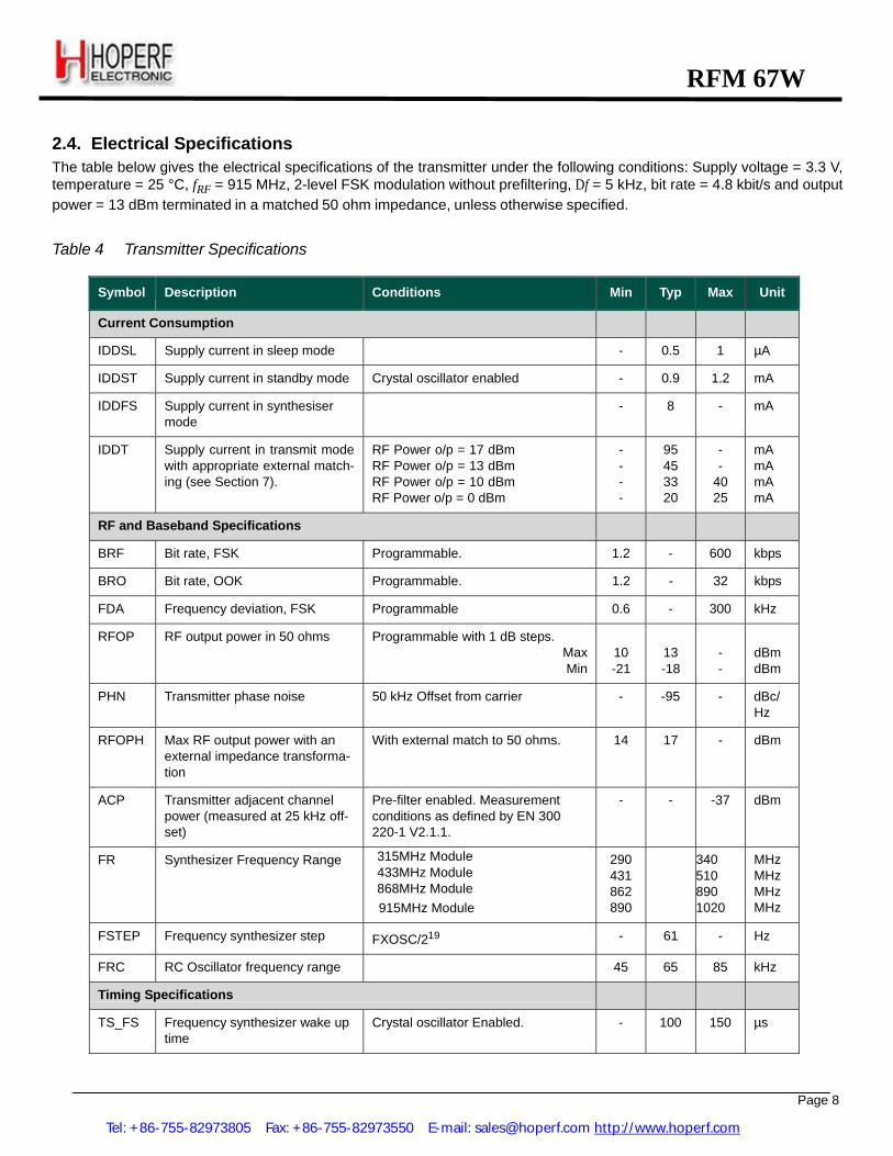
RFM 67W 2.4. Electrical Specifications The table below gives the electrical specifications of the transmitter under the following conditions: Supply voltage = 3.3 V, temperature = 25 °C, fRF = 915 MHz, 2-level FSK modulation without prefiltering, Df = 5 kHz, bit rate = 4.8 kbit/s and output power = 13 dBm terminated in a matched 50 ohm impedance, unless otherwise specified.
Table 4 Transmitter Specifications
Symbol Description Conditions Min Typ Max Unit
Current Consumption IDDSL Supply current in sleep mode - 0.5 1 µA IDDST Supply current in standby mode Crystal oscillator enabled - 0.9 1.2 mA IDDFS Supply current in synthesiser
mode - 8 - mA
IDDT Supply current in transmit mode with appropriate external match- ing (see Section 7).
RF Power o/p = 17 dBm RF Power o/p = 13 dBm RF Power o/p = 10 dBm RF Power o/p = 0 dBm
- - - -
95 45 33 20
- -
40 25
mA mA mA mA
RF and Baseband Specifications BRF Bit rate, FSK Programmable. 1.2 - 600 kbps BRO Bit rate, OOK Programmable. 1.2 - 32 kbps FDA Frequency deviation, FSK Programmable 0.6 - 300 kHz RFOP RF output power in 50 ohms Programmable with 1 dB steps.
TS_TR Transmitter wake-up time Frequency synthesizer enabled. Note, depends upon bit rate and ramp time, please refer to Section 7.4.
- 120 - µs
TS_OS Crystal oscillator wake-up time - 300 500 µs FXOSC Crystal oscillator frequency For All Module 32 MHz TS_TT Total Wake up time Sleep to transmit, automated. Note,
depends upon bit rate and ramp time, please refer to Section 7.4.
- 450 - µs
T_DATA Data set-up time - - 0.25 µs 3. Timing Characteristics The following table gives the operating specifications for the SPI interface of the RFM67W. Table 5 SPI Timing Specifications
Symbol
Description
Conditions
Min
Typ
Max
Unit
fSCK SCK Frequency - - 10 MHz
tch SCK High time 50 - - ns
tcl SCK Low time 50 - - ns
trise SCK rise time - 5 - ns
tfall SCK Fall time - 5 - ns
tsetup
MOSI Setup time From MOSI transition to SCK rising edge
30 - - ns
thold MOSI hold time From SCK rising edge to MOSI tran- sition
20 - - ns
tnl NSS setup time From NSS falling edge to SCK rising edge
30 - ns
tnh,n NSS Hold time From SCK falling edge to NSS rising edge.
30 - - ns
For explanatory diagrams of the timing characteristic parameters, please see Figure 7 and Figure 8.
4.1. Operating Modes The four operating modes of the RFM67W are shown in Table 6. Each of these may be selected via the SPI bus by writing the corresponding bits to Mode(2:0). A key feature of the RFM67W is that the transition from one operating mode to the next is automatically optimized. For example, if the transmit operating mode is selected whilst in sleep operating mode then, in a pre-defined time-optimized sequence, each of the intermediate modes is engaged sequentially without the need to issue any further SPI commands. For more information on timing and optimization please see Section 7.4.
Table 6 RFM67W Operating Modes
Enabled Blocks
MODE(2:0)
Selected Mode
RC Osc
SPI
Xtal Osc
Freq. Synth.
PA
000 Sleep mode Optional x 001 Stand-by mode Optional x x 010 FS mode Optional x x x 011 Transmit mode Optional x x x x
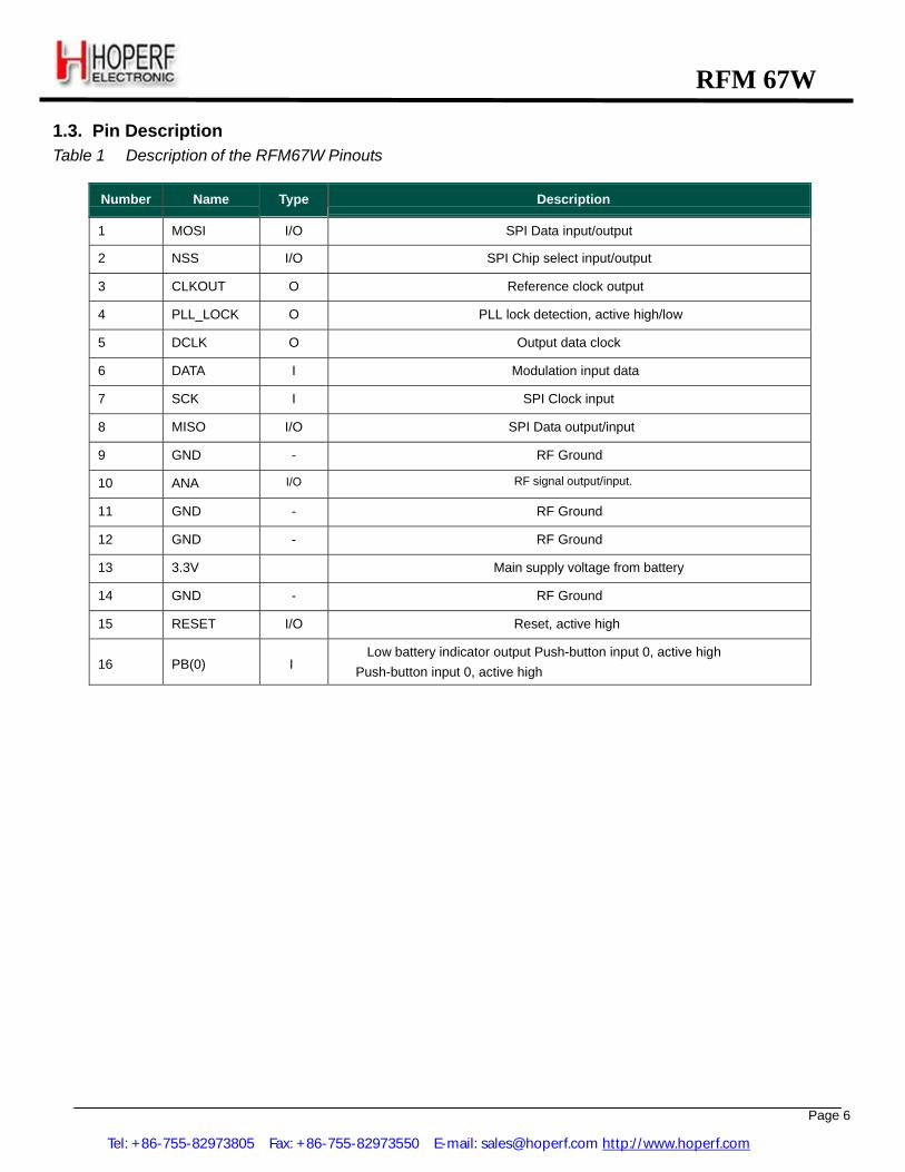
4.2. Application Modes The RFM67W has two application modes, selected by applying an external logical level to the E2_MODE input. The first, MCU mode (E2_Mode= ‘0’), configures the RFM67W as an SPI slave. This permits the configuration of the circuit by an external microprocessor via the SPI interface of the RFM67W and the data to be applied via the DATA input (pin 13). The second application mode, stand-alone mode (E2_Mode = 0), sees the RFM67W configured as SPI master. In the stand- alone application mode the RFM67W can download its configuration from an external SPI E2PROM. Moreover, in response to an input on the GPIO pins, a specific configuration can be programmed and a payload transmitted. Note that this mode selection process is performed at start up (or POR) of the circuit. Thus the hardware mode cannot be dynamically changed without resetting the chip. This may be achieved either by power down or by issuing an active high POR signal to the Reset input. For reset signal timing please see the diagram of Figure 13 and accompanying description.
4.2.1. Stand Alone Mode In stand alone mode (E2_Mode = ‘1’) the RFM67W will operate as a stand-alone SPI master which can download both register settings and data payload from an SPI E2PROM. Four debounced GPIO inputs are available in stand alone mode, in this application mode the RFM67W remains in sleep operating mode until either a single or combination of button presses are detected. RFM67W can then be dynamically reconfigured and / or transmit a data sequence stored within the E2PROM.
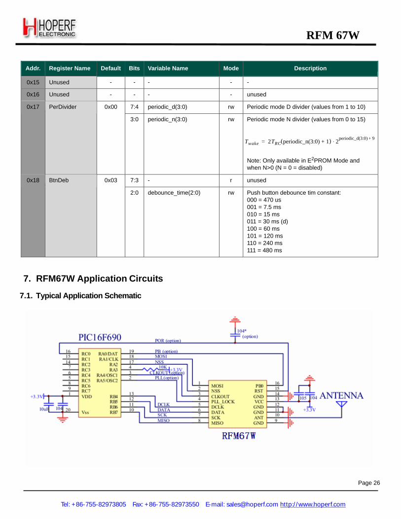
The RFM67W can accommodate SPI E2PROM sizes up to 8 kbit and uses industry standard SPI commands. For a full description of E2PROM use with RFM67W and the associated application circuits, please see Section 6.1. The application circuit for stand-alone operation is shown in Figure 3, note that both matching and LM are band specific whilst CTX is application specific.
Figure 3. RFM67W Stand-Alone Application Circuit 4.2.2. MCU Mode The RFM67W is also capable of operating in a conventional MCU controlled mode. Figure 4 shows the RFM67W operating in MCU mode and connected to an external microcontroller. Note that CLKOUT provides the oscillator signal for the MCU, thus negating the need for two crystal oscillators. The DCLK connection is also optional - only being required if the data rate is to be determined by RFM67W or transmit filtering is to be used.
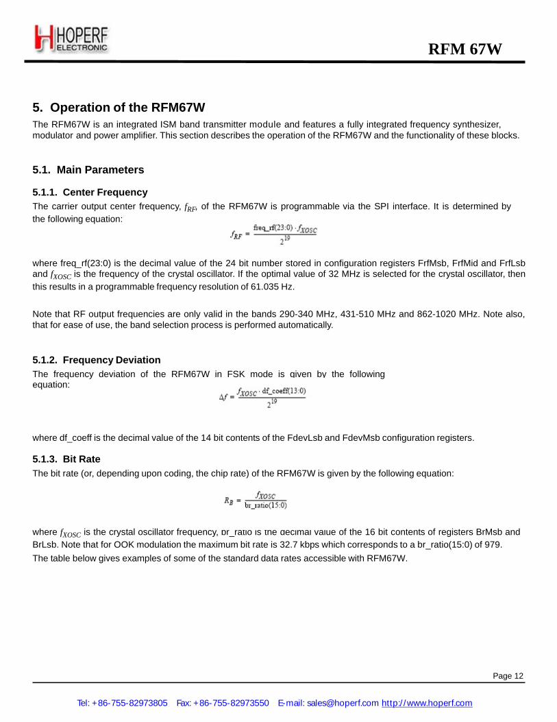
ADVANCED COMMUNICATIONS & SENSING DATASHEET 5. Operation of the RFM67W The RFM67W is an integrated ISM band transmitter module and features a fully integrated frequency synthesizer, modulator and power amplifier. This section describes the operation of the RFM67W and the functionality of these blocks.
5.1. Main Parameters
5.1.1. Center Frequency The carrier output center frequency, fRF, of the RFM67W is programmable via the SPI interface. It is determined by the following equation:
where freq_rf(23:0) is the decimal value of the 24 bit number stored in configuration registers FrfMsb, FrfMid and FrfLsb and fXOSC is the frequency of the crystal oscillator. If the optimal value of 32 MHz is selected for the crystal oscillator, then this results in a programmable frequency resolution of 61.035 Hz.
Note that RF output frequencies are only valid in the bands 290-340 MHz, 431-510 MHz and 862-1020 MHz. Note also, that for ease of use, the band selection process is performed automatically.
5.1.2. Frequency Deviation The frequency deviation of the RFM67W in FSK mode is given by the following equation: where df_coeff is the decimal value of the 14 bit contents of the FdevLsb and FdevMsb configuration registers.
5.1.3. Bit Rate The bit rate (or, depending upon coding, the chip rate) of the RFM67W is given by the following equation:
where fXOSC is the crystal oscillator frequency, br_ratio is the decimal value of the 16 bit contents of registers BrMsb and BrLsb. Note that for OOK modulation the maximum bit rate is 32.7 kbps which corresponds to a br_ratio(15:0) of 979. The table below gives examples of some of the standard data rates accessible with RFM67W.
5.2. Synthesizer The frequency synthesizer of the RFM67W is a fully integrated fractional-N third-order sigma-delta phase-locked loop and VCO. Also incorporated are fully integrated third-order and low pass filters which determine the loop bandwidth. All of these features are fully automated and derived from the user bitrate and frequency deviation settings, as described in Sections 5.1.1 to 5.1.3.
To ensure the frequency accuracy of the PLL output it is necessary to perform calibration. The calibration process is performed automatically upon power up of the RFM67W. However, the calibration feature is also accessible to the user via the SPI configuration register, PllStat (address 0x0A). The calibration is performed by setting bit 2 (pll_cal) high. This ensures that the frequency output accuracy is limited only by the frequency error of the crystal oscillator, the calibration procedure lasts 500 µs, during which time pll_cal_done (bit 4 of address 0x0A) is set low. Once complete pll_cal_done is set high and confirmation of a successful calibration can be obtained by reading pll_cal_ok.
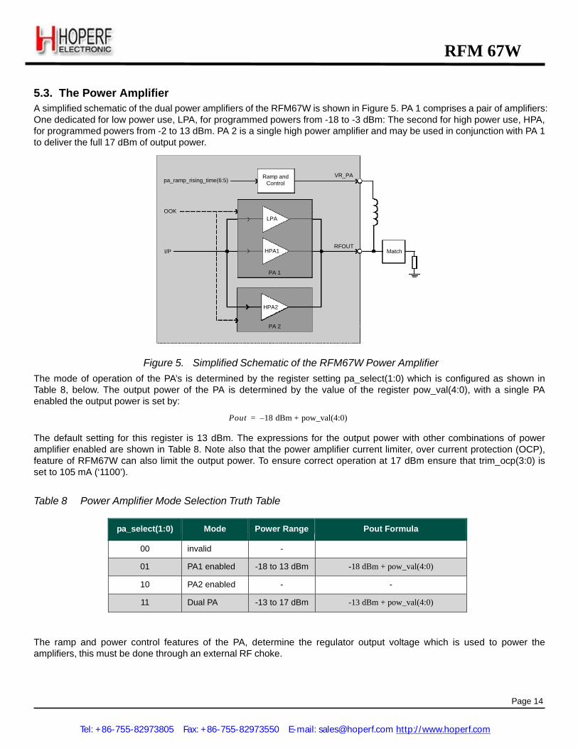
5.3. The Power Amplifier A simplified schematic of the dual power amplifiers of the RFM67W is shown in Figure 5. PA 1 comprises a pair of amplifiers: One dedicated for low power use, LPA, for programmed powers from -18 to -3 dBm: The second for high power use, HPA, for programmed powers from -2 to 13 dBm. PA 2 is a single high power amplifier and may be used in conjunction with PA 1 to deliver the full 17 dBm of output power.
pa_ramp_rising_time(6:5) Ramp and Control
VR_PA
OOK LPA
I/P HPA1
RFOUT Match
PA 1
HPA2
PA 2
Figure 5. Simplified Schematic of the RFM67W Power Amplifier The mode of operation of the PA’s is determined by the register setting pa_select(1:0) which is configured as shown in Table 8, below. The output power of the PA is determined by the value of the register pow_val(4:0), with a single PA enabled the output power is set by:
Pout = –18 dBm + pow_val(4:0)
The default setting for this register is 13 dBm. The expressions for the output power with other combinations of power amplifier enabled are shown in Table 8. Note also that the power amplifier current limiter, over current protection (OCP), feature of RFM67W can also limit the output power. To ensure correct operation at 17 dBm ensure that trim_ocp(3:0) is set to 105 mA (‘1100’).
Table 8 Power Amplifier Mode Selection Truth Table
pa_select(1:0) Mode Power Range Pout Formula
00 invalid - 01 PA1 enabled -18 to 13 dBm -18 dBm + pow_val(4:0) 10 PA2 enabled - - 11 Dual PA -13 to 17 dBm -13 dBm + pow_val(4:0)
The ramp and power control features of the PA, determine the regulator output voltage which is used to power the amplifiers, this must be done through an external RF choke.
6. Digital Control and Interface The RFM67W has several operating modes, configuration parameters and internal status indicators which are stored in internal registers. In MCU mode, all of these registers can be accessed by an external microcontroller via the SPI interface. In stand alone mode, both the configuration information and the data to be transmitted, are stored in an external E2PROM. The way that both the configuration and payload information is stored in the E2PROM must match the way the configuration is defined in the internal registers. For a full description see Section 6.1.2.
6.1. Stand Alone Mode
6.1.1. State Machine Description The stand alone mode is activated when the pin E2_Mode is tied to VDD. The RFM67W SPI interface is then configured in master mode. The internal state machine of the RFM67W then carries out the following operations:
1) Immediately after power-up, the SPI interface reads the main configuration section in the E2PROM and then goes into the ‘sleep’ operating mode (i.e. all blocks off).
2) Whilst in ‘sleep’ operating mode, when an edge is detected on any of the push-buttons PB[3:0], the chip wakes-up and starts the RC oscillator (typical startup time ~100 µs).
3) The RC oscillator is used to clock a debounce timer which gives the logical push button input value after the programmed delay. The frame section corresponding to the button value (1 to 15) is read from the E2PROM. At this point additional, button specific, configuration information may be loaded. Otherwise, the configuration settings of 1) are used. Using the appropriate configuration, the payload corresponding to the detected button press is then transmitted. The payload transmission may be repeated up to 254 times.
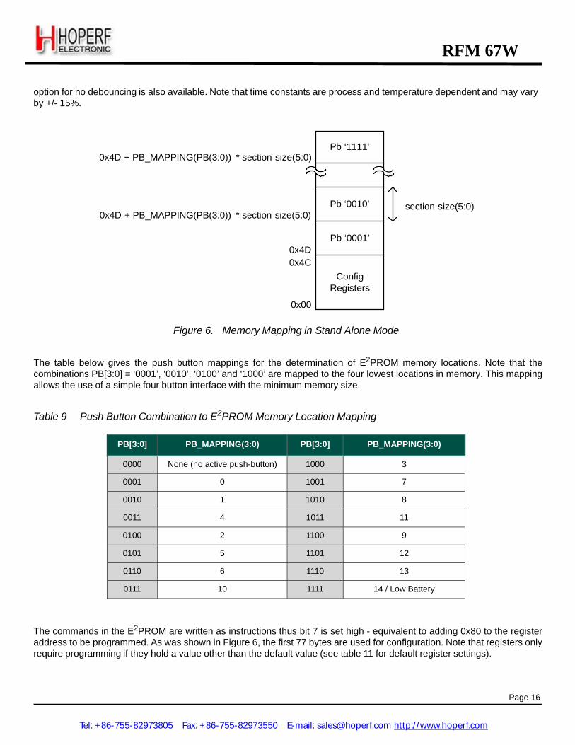
4) When the frame has been transmitted, the pad PLL_LOCK goes low and the chip goes into SLEEP mode. 6.1.2. Memory Organization of the E2PROM The memory map for stand alone mode is shown in Figure 6. The configuration information occupies the first 77 bytes, the format of the configuration is {ADDR; VALUE} - therefore allowing up to 38 registers to be defined. Each push button configuration is mapped directly to a location in the E2PROM - determined by the mappings given in Table 9 and the variable section_size(5:0). The purpose of this variable, push button specific, section size is to allow the optimum use of different sizes of external memory. Note that the maximum frame length is 64 bytes - this equates to a maximum E2PROM size of 8 kbit. The influence of the section_size variable is illustrated in Figure 6.
The mapping of Table 9 permits up to 15 frames to be defined. Each section may contain both write_registers commands and the payload to be transmitted. Thus allowing the dynamic configuration of settings such as output power and frequency in response to a button push. Each section within the E2PROM must conform to the following format: {FIFO_ADDR; REPEAT; LENGTH; VALUE_1; VALUE_2;...;VALUE_N}. Where VALUE_1... N is the user defined payload, REPEAT is the number of times the frame is to be transmitted, LENGTH defines the number of bytes in the message and FIFO_ADDR = 0x95.
The push-buttons may need to be debounced before being read. The debouncer time constant is programmed by the debounce_time(2:0) register which allows a range of debounce timer values to be accessed from 470 ms to 480 ms. An
The table below gives the push button mappings for the determination of E2PROM memory locations. Note that the combinations PB[3:0] = ‘0001’, ‘0010’, ‘0100’ and ‘1000’ are mapped to the four lowest locations in memory. This mapping allows the use of a simple four button interface with the minimum memory size.
Table 9 Push Button Combination to E2PROM Memory Location Mapping
The commands in the E2PROM are written as instructions thus bit 7 is set high - equivalent to adding 0x80 to the register address to be programmed. As was shown in Figure 6, the first 77 bytes are used for configuration. Note that registers only require programming if they hold a value other than the default value (see table 11 for default register settings).
The following table gives an example snippet of E2PROM contents, here for each location in E2PROM memory the first 13 bytes of the available 77 (0x4C) bytes are occupied with configuration. The remaining bytes are left in their default 0xFF setting. The first push-button memory location is at 0x4D. Here we see that the periodic mode timer (see following section for a full description) is configured and a 10 byte payload follows. Subsequent push buttons are configured at the locations determined by the section size, see Figure 6.
Table 10 Example External SPI E2PROM Contents for RFM67W Configuration
Subsequent button push button configuration and payload could follow at address 0x5C, respecting the E2PROM section size constraint. Note that if register 0x00 is configured, care should be taken to enable transmit mode - mode(2:0) to ensure reliable transition to transmit mode.
6.1.3. Periodic mode Periodic mode is a sub-mode of stand alone mode wherein the RFM67W will periodically sense the push button inputs for activity. If a push button input is high then the payload according to that input is transmitted. The wake-up interval, Twakeup, is defined by periodic_n(3:0) and periodic_d(3:0) values.
where TRC is the RC oscillator period, periodic_n is programmable between 0 and 15 and periodic_d may take values between 0 and 10. The maximum period is hence approximately 125 s when the frequency of the RC oscillator is 67 kHz. Push button mode is enabled when the value of D is non-zero and, when activated, all stand alone mode functionality is available. It is important to note that if there is no push button pressed, then no message will be transmitted.
6.1.4. Low Battery Indicator: Stand Alone Mode
The low battery indicator may be used in stand alone mode to detect the battery voltage and send a low battery message to the receiver. It is enabled by setting the eol_frame_mode bit ‘high’ (register 0x12). The low battery state is determined by comparing the supply voltage with a 1.695 V to 2.185 V programmable threshold (threshold trim_eol(2:0), address 0x12). Following detection, the following actions are performed depending upon the exact mode of operation:
Normal Operation (Non-Periodic): The battery end-of-life condition is checked during the normal frame. If it is true, then a single extra frame #14 (see Table 9) is automatically sent after the normal frame.
Stand-Alone Periodic Mode Operation: The battery end-of-life condition is checked during the normal frame. If it is true, then the next frame, sent at the next timer tick is frame #14 (see Table 9), the frame is sent only once.
6.1.5. Low Battery Indicator: MCU Mode In MCU mode the low battery status indicator may be accessed and configured via the SPI register EolCtrl. Alternatively, the active high low battery indication is mapped to the PB0 pin allowing the independent generation of hardware interrupts.
6.2. MCU Mode
6.2.1. SPI Operation The first byte in any data transfer over the SPI is the address read/write byte. It comprises:
1. W/RB bit, which is 1 for write access and 0 for read access 2. 7 bits of address, MSB first.
A transfer always starts by the NSS (not slave select) signal going low whilst SCK is high. MOSI (master out - slave in) is generated by the master on the next falling edge of SCK and is sampled by the slave on the next rising edge of SCK. MISO is generated by the slave on the falling edge of SCK and is high impedance when NSS is high. By convention, all bytes are sent MSB first.
MCU mode is activated when pad E2_Mode is tied to GND (ground). In this mode the RFM67W is configured as SPI slave and its internal configuration registers can be written following the format shown in Figure 7.
An ‘address write-byte‘ followed by a data byte is sent for a write access. Where multiple sequential registers are to be written, the NSS input may be kept low after this first address-byte plus data-byte have been sent. In this state sequential data-bytes may be written, the address is automatically incremented after the reception of each additional data-byte. This allows the sequential data-bytes to be written without the need for an address byte. NSS must then be set ‘high’ after the last byte transfer.
Similarly, the configuration registers of the RFM67W can be read by issuing an ‘address read-byte’ (see Figure 8) the corresponding register contents are then transferred over the MISO line. As above, the contents of each subsequent register can be transferred by holding the NSS input low.
A summary of all of the registers of the RFM67W are given in Table 11, this is followed by detailed descriptions of each of the registers in Table 12.
6.2.2. Data and Data Clock Usage In MCU mode the data to be transmitted is applied exclusively via the DATA input. The DATA input is sampled at the crystal frequency, fxosc. Where the MCU mediates the data rate and no gaussian or bit filtering is required, then the use of the data clock signal is optional. However, where filtering is to be used or the specified data rate accuracy is to be achieved, then the rising edge of the data clock, DCLK, signal must be used to clock the data into the RFM67W DATA input.
T_DATA T_DATA
DATA (NRZ)
DCLK
Figure 9. RFM67W Data Clock Timing Diagram (Used Only for Filtering and Ensuring Bit Rate Accuracies)
0x08 PaCtrl PA selection and power control. 0x09 PaFskRamp PA rise and fall timing (FSK). 0x0A PllStat PLL status register. 0x0B VcoCtrl1 0x0C VcoCtrl2 0x0D VcoCtrl3 0x0E VcoCtrl4
VCO calibration values.
0x0F ClockCtrl Clock output pin settings. 0x10 Eeprom Stand alone mode E2PROM configuration. 0x11 ClockSel Selection between RC or crystal oscillator. 0x12 EolCtrl Low battery indicator settings. 0x13 PaOcpCtrl PA Over current protection - limits PA current. 0x14 unused - 0x15 unused - 0x16 unused - 0x17 PerDivider Periodic mode wake-up timer control. 0x18 BtnDeb Push button debouncer setting.
1:0 data_shaping(1:0) rw Data shaping: In FSK: 00 no shaping 01 Gaussian filter with BT = 1.0 10 Gaussian filter with BT = 0.5 11 Gaussian filter with BT = 0.3 In OOK: 00 no shaping 01 filtering with fcutoff = bit rate 10 filtering with fcutoff = 2 * bit rate (BR <= 32 kb/s) 11 reserved
0x01 BrMsb 0x1A 7:0 br_ratio(15:8) rw Bit rate MSB (chip rate if Manchester encoding)
0x02 BrLsb 0x0B
7:0 br_ratio(7:0) rw Bit rate LSB (chip rate if Manchester encoding)
Default value is 0x1A0B = 4.8 kbps 7:6 - - unused 0x03 FdevMsb 0x00 5:0 fdev_coeff(13:8) rw Deviation frequency MSB
0x04 FdevLsb 0x52 7:0 fdev_coeff(7:0) rw Deviation Frequency LSB
4:0 pow_val(4:0) rw Output power Pout = -18 dBm + pow_val Default is 13 dBm.
7:4 - r unused 0x09 PaFskRamp 0x08 3:0 pa_ramp_rising_time(3:0) rw Rise/fall time ramping (FSK only)
0000 = 2 ms 0001 = 1 ms 0010 = 500 us 0011 = 250 us 0100 = 125 us 0101 = 100 us 0110 = 62 us 0111 = 50 us 1000 = 40 us (d) 1001 = 31 us 1011 = 25 us 1010 = 20 us 1100 = 15 us 1101 = 12 us 1110 = 10 us 1111 = 8 us
Addr. Register Name Default Bits Variable Name Mode Description
7:6 - r unused 5 pll_lock_detect r PLL lock status:
0 = PLL not locked 1 = PLL locked
4 pll_cal_done r PLL calibration status 0 = Calibration on-going 1 = Calibration performed Note: Reset to 0 in sleep mode irrespective of calibration state.
3 pll_cal_ok r PLL Calibration Result 0 = Calibration procedure failed 1= Calibration procedure successful Note: Reset to 0 in sleep mode irrespective of calibration state
2 pll_cal_start w Triggers PLL calibration, always read as 0.
7:5 - r unused 0x0B VcoCtrl1 NA 4:0 SB1(4:0) rw VCO band first calibration value 7:5 - r unused 0x0C VcoCtrl2 NA 4:0 SB2(4:0) rw VCO band second calibration value 7:5 - r unused 0x0D VcoCtrl3 NA 4:0 SB3(4:0) rw VCO band third calibration value 7:5 - r unused 0x0E VcoCtrl4 NA 4:0 SB4(4:0) rw VCO band fourth calibration value 7:4 - r unused 3 rc_enable rw
Enables RC oscillator. RC oscillator is also automatically switched on in E2PROM mode. 0 = RC oscillator off 1 = RC oscillator on
2:0 vthr_eol(2:0) rw Battery end of life threshold 000 = 1.695 V 001 = 1.764 V 010 = 1.835 V (default setting) 011 = 1.905 V 100 = 1.976 V 101 = 2.045 V 110 = 2.116 V 111 = 2.185 V
7:5 - r unused 4 on_ocp rw
Enables power amplifier current limiter: 0 = OCP disabled 1 = OCP enabled
0x13 PaOcpCtrl 0x11
3:0 trim_ocp(3:0) rw PA OCP DC load current threshold: 0000 = 45 mA 0001 = 50 mA 0010 = 55 mA 0011 = 60 mA 0100 = 65 mA 0101 = 70 mA 0110 = 75 mA 0111 = 80 mA 1000 = 85 mA 1001 = 90 mA 1010 = 95 mA 1011 = 100 mA (default setting) 1100 = 105 mA (recommended +17 dBm setting)1101 = 110 mA 1110 = 115 mA 1111 = 120 mA
Addr. Register Name Default Bits Variable Name Mode Description
0x15 Unused - - - - - 0x16 Unused - - - - unused
7:4 periodic_d(3:0) rw Periodic mode D divider (values from 1 to 10) 0x17 PerDivider 0x00 3:0 periodic_n(3:0) rw Periodic mode N divider (values from 0 to 15)
7.2. Wake-up Times When switching between modes, an optimized sequence of events is automatically performed by RFM67W. For example, in response to the command to enter transmit mode whilst in sleep mode, each intermediate mode is engaged - ensuring crystal oscillator start-up and PLL lock before transition to transmit mode. External indication of PLL lock is given by the PLL lock pin (MCU mode only). The PLL lock pin output is only valid whist no data is applied to the DATA pin. The transition from frequency synthesizer mode to transmit is well defined and a function of bit rate and transmit ramp time, given in FSK mode by:
where pa_ramp_rising_time(3:0) is the user defined contents of PaFskRamp and RB is the bit rate. For OOK mode the time is given by:
TS_TS (μs ) = 5 + ------1------- 2 · RB
A flow chart showing the automatic, optimised start-up procedure, initiated with a single SPI command is shown in Figure 14. Note that after the PLL lock indicator is set then the transmitter requires TS_TR to set-up before transmission may begin.
7.3 Reset Pin Timing Manual reset of the RFM67W is possible by asserting a logical high to the reset pin. The timing for this operation is shown in the following figure. During the reset operation the RFM67W current consumption may rise to 1 mA. Following the reset operation the user must wait 5 ms before performing any other operation.
8. Reference Design Performance This section details the measured typical performance of the reference design described in the preceding section.
8.1. Power Output versus Consumption
20 90
17 dBm Match Pmeas
15 14 dBm Match Pmeas 80 17 dBm Match Imeas 14 dBm Match Imeas
10 70
5 60
0 50
-5 40
-10 30
-15 20
-20 PA1 Only PA1 and 2 Enabled
10 -20 -15 -10 -5 0 5 10 15 20
Programmed Power (dBm)
Figure 24. Typical Power Consumption of the Reference Design versus Measured and Programmed Power Output at 915 MHz
The measured current consumption of the RFM67W versus programmed and measured output power is shown in the preceding figure. The green curves correspond to measurements (made at 915 MHz) using the low power matching of Section 7.7. The measured consumption displays two distinct regimes: Above a programmed power of -3 dBm both high and low power amplifiers of PA1 are active. Below, however, only the low power amplifier within PA1 is enabled allowing enhanced efficiency for operation below this programmed power output.
The blue portion of the curve (13 to 17 dBm operation) uses the matching illustrated in Section 7.6. Note that not only must both power amplifiers be enabled to access these output powers, but also the OCP (current limiter) for the PA must be disabled or the limit adjusted to 100 mA accordingly.
8.2. Power Output Flatness versus Temperature and Supply Voltage The RFM67W reference design power output flatness as a function of voltage and temperature is shown below.
16.90
16.80
16.70
16.60
16.50
3.6 V, 25 C 3.3 V, 25 C 1.8 V, 25 C 3.6 V, 90 C 3.3 V, 90 C 1.8 V, 90 C 3.6 V, -45 C 3.3 V, -45 C 1.8 V, -45 C
16.40
16.30 862 863 864 865 866 867 868 869 870 871
Frequency (MHz)
Figure 25. Typical 17 dBm Output Power Flatness versus Supply Voltage and Temperature, Measured in the 868 MHz ISM Band
17.40
17.30
17.20
17.10
17.00
16.90
3.6 V, 25 C 3.3 V, 25 C 1.8 V, 25 C 3.6 V, 90 C 3.3 V, 90 C 1.8 V, 90 C 3.6 V, -45 C 3.3 V, -45 C 1.8 V, -45 C
16.80
16.70
16.60 900 905 910 915 92 0 92 5 93 0
Freque nc y (MHz)
Figure 26. Typical 17 dBm Output Power Flatness versus Supply Voltage and Temperature, Measured in the 915 MHz ISM band
27. Typical RF67 Phase Noise Measurement at 315 MHz (-104 dBc/Hz at 5
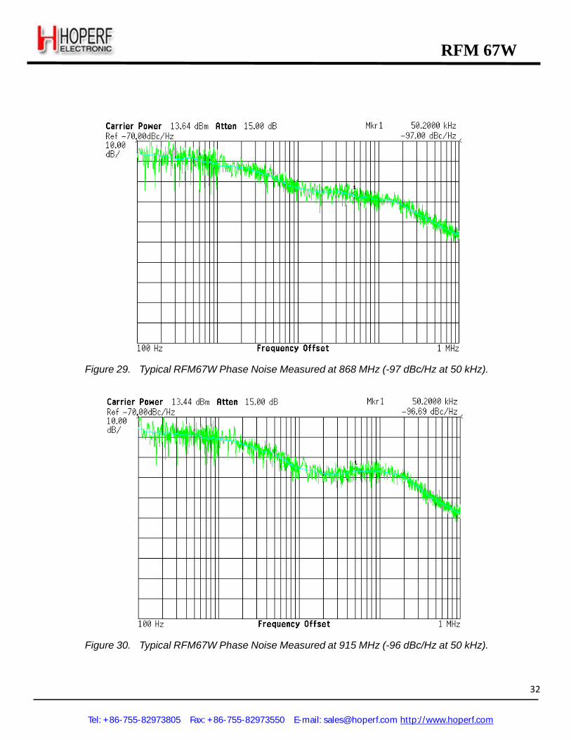
8.3. Phase Noise The phase noise of the RFM67W is measured in the centre frequencies of the principal ISM bands below 1 GHz. The phase noise is a function of frequency and varies from -104 dBc/Hz at 50 kHz offset at 315 MHz band to -96dBc/Hz at 50 kHz offset at 915 MHz
Figure 0 kHz).
Figure 28. Typical RFM67W Phase Noise Measurement at 434 MHz (-102 dBc/Hz at 50 kHz).
Figure 27. Typical RFM67W Phase Noise Measurement at 315 MHz (-104dBc/Hz at 50 kH )
8.4. RFM67W Baseband Filtering The following figure illustrates the effect of applying the baseband gaussian filtering to the modulating bitstream of the RFM67W. This measurement was performed in the 868 MHz ISM band with the following settings: PPGM = 17 dBm, fRF = 868 MHz, Df = 50 kHz and Rb = 50 kbps (implies b=2). Here we see the occupied bandwidth reduced from 500 kHz for the unfiltered bit stream to 330 kHz with a filtering coefficient (BT) of 1. By increasing the filtering strength further to BT=0.3, the channel bandwidth for operation in the 868 MHz ISM band is reduced to below 200 kHz.
Figure 31. The Influence of Gaussian Filtering on the Modulation Bandwidth (Wideband) 8.5. Adjacent Channel Power Modulation spectrum of the RFM67W measured in 100 Hz bandwidth is shown in the following three figures together with the integrated adjacent channel power for the modulation settings shown in the figure caption. Please note that all measurements were performed at 868 MHz, with an output power of 13 dBm. Please also note that the clock output was disabled.