Page 1
1
Ripple Texturing of Suspended Graphene Atomic Membranes
Wenzhong Bao1, Feng Miao1, Zhen Chen2, Hang Zhang1, Wanyoung Jang2, Chris Dames2,
Chun Ning Lau1*
1Department of Physics and Astronomy, University of California, Riverside, CA 92521
2Department of Mechanical Engineering, University of California, Riverside, CA 92521
Abstract
Graphene is the nature’s thinnest elastic membrane, with exceptional mechanical and electrical
properties. We report the direct observation and creation of one-dimensional (1D) and 2D
periodic ripples in suspended graphene sheets, using spontaneously and thermally induced
longitudinal strains on patterned substrates, with control over their orientations and wavelengths.
We also provide the first measurement of graphene’s thermal expansion coefficient, which is
anomalously large and negative, ~ -7x10⁻⁶ K-1 at 300K. Our work enables novel strain-based
engineering of graphene devices.
PACS numbers: 62.25.-g, 65.40.De, 68.55.-a, 73.63.-b
* E-mail: [email protected]
Page 2
2
As the only known isolated atomic membrane[1-3], graphene offers a unique platform for
understanding the fundamental mechanical properties of nano-materials, such as its extremely
high elastic constants[4] and breaking strength[5], and the spontaneous formation of ripples in
suspended graphene [6]. Unlike other thin films, the local mechanical distortions in graphene are
expected to have a profound impact on its electrical properties, including creating effective
magnetic fields[7, 8], modifying the local electronic potential[9, 10], breaking the charges’
valley degeneracy[8], and inducing additional scattering[11, 12]. Such a close relationship
between graphene’s morphology and electrical properties, and its readiness to deform, could be
explored to enable device tailoring based on manipulation of local strains[13], or to facilitate
selective formation of sp3 carbon-carbon bonds for bandgap creation[14]. However, even though
corrugations have been inferred from finite-sized electron diffraction spots in suspended
graphene sheets[6], ripples have neither been directly observed or controlled.
Here we report the direct observation and controlled creation of periodic ripples in
suspended graphene sheets via spontaneously and thermally generated strains. We find that thin
film mechanics, developed for continuum materials, continues to describe these atomically thin
membranes. We manipulate the orientation, wavelength and/or amplitude of the ripples via
controlled boundary conditions and the difference in the thermal expansion coefficients (TEC)
between graphene and the substrate. This thermo-mechanical manipulation is especially effective
because of graphene’s anomalously large and negative TEC, which is measured to be ~5-6 times
larger than that of bulk graphite in the basal plane. Finally, as a first step towards systematic
investigation of ripple-related transport effects, we perform electrical measurements on these
graphene devices. Our results indicate that small ripples do not introduce significant scattering,
Page 3
3
consistent with prior results[15, 16], and shed light on some of the unusual behaviors observed in
ref. [16].
Graphene membranes, ranging from single layers (~0.3 nm) to ~ 16 nm in thickness, and
~0.5 to 20 µm in width, are suspended across pre-defined trenches on Si/SiO2 substrates[17]. We
examine their morphology under a scanning electron microscope (SEM) or an atomic force
microscope (AFM). Strikingly, most of the graphene sheets are not flat, but spontaneously form
nearly periodic ripples (Fig. 1a-c). Typically, the ripple crests are perpendicular to the edges of
the trench (y-direction), although oblique ripples are also occasionally observed[17]. The out-of-
plane displacement ζ of the ripples is well-described by a sinusoidal function,
ζ =Asin(2πy/λ). (1)
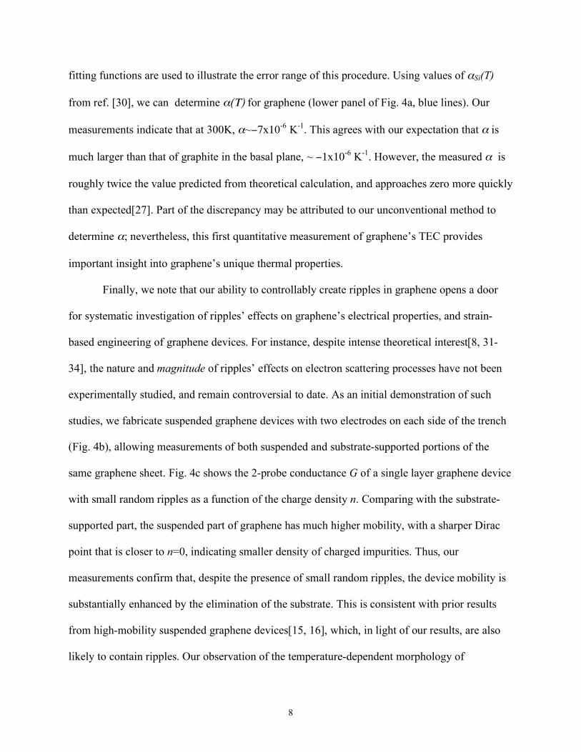
where A is the amplitude and λ the wavelength. We have imaged and measured more than 50
different membranes, with A ranging from 0.7 to 30 nm, and λ ranging from 370 nm to 5 µm.
To understand the origin of these ripples, we note that for an elastic thin film, ripples
described by Eq. (1) may be induced by either transverse compression in the y direction, or by
longitudinal strain and/or shear in the x-direction[18]. From classical elasticity theory[19], we
expect the clamped boundary conditions imposed by the banks of the trenches suppress lateral
movement and induce local biaxial stress. For a thin film of thickness t with clamped boundaries
at x=0 and x=L, the presence of a longitudinal tensile strain γ leads to[18]
!
"4
tL( )2
=4# 2
3 1$% 2( )& and
!
A2
"tL=
16#
3$ 2 (1%" 2 )
&
' (
)
* +
1/2
(2)
Here ν =0.165 is the Poisson ratio for graphite in the basal plane[20]. Combining both equations,
we eliminate γ and obtain a relation with only experimentally accessible parameters:
Page 4
4
!
A"
L=
8#
3(1$# 2 )t (3)
If instead the applied stress is dominated by in-plane shear, the equation takes a different
prefactor[21]
!
A"
L=
8
3(1+ # )t (4)
Using values of A, L, λ and t as determined from AFM images, we plot Aλ/L vs. t for 51 devices
that display periodic ripples, as shown by the data in Fig. 1d. Eqs. (3) and (4) are plotted as the
lower and upper lines, respectively. Most of the data points fall on the lower solid line, indicating
that the ripples are induced by pre-existing longitudinal strains in graphene. However, the 6 data
points that fall above the upper line have a similar slope to the latter, suggesting the presence of
shear in these devices.
Eqs. (2) – (4) are derived based on classical thin-film elasticity theory, and may not be
valid a priori for atomically thin membranes. The inset of Fig. 1d displays Aλ/L vs. t for samples
that are 1, 2 and 3 layers thick. Remarkably, the data points falls on a straight line, suggesting
that Eq. (3) holds even for single atomic layer membranes.
The strains in these atomic membranes can also be readily obtained from Eq. (2). In Fig.
1e, we use the first equation to compute γ for membranes with strain-induced ripples, and plot γ
vs t. For thicker films, γ is relatively small, ~0.016% to 0.3%. In contrast, thinner films are more
easily strained, and exhibit γ up to 1.5%.
Building on our observation of periodic ripples in graphene membranes, we now show
that these ripples can be controllably produced via simple thermal manipulation. The graphene
membranes are annealed in a furnace in argon up to 700 K, and imaged again at room
temperature. Surprisingly, almost all graphene membranes undergo one or both of the following
Page 5
5
dramatic changes in morphology – (1) the ripple geometry is significantly altered, with
apparently larger amplitudes and longer wavelengths; (2) the graphene membrane buckles,
typically sagging toward the substrate, or occasionally buckling upwards. In fact, the buckling
can be quite dramatic: the central portions of several membranes settled on the bottom of the
trenches without breaking[17].
To understand these observations, we perform in situ SEM imaging of our devices at
different temperatures T, using a custom-built SEM stage with a built-in heater and a
thermocouple. Fig. 2a-b show two image sequences for two different membranes. When T is
raised to 450-600K, the membranes are flat, and any pre-existing ripples completely disappear.
However, upon cooling down to 300K, ripples invariably appear, usually with much larger
amplitudes than any pre-annealing ones. The device in Fig. 2b also exhibits longitudinal
buckling and sags into the trench. A movie of ripple formation in a single-layer graphene film
during cooling is included online[17].
The above observations suggest that, after thermal annealing, a graphene sheet
experiences biaxial compression[22]; the different behaviors (rippling vs. buckling) arise from
the different boundary conditions in the two directions. This process may be understood in terms
of graphene’s thermal contraction, and the competition between three forces: (1). Fpin, the
substrate-pinning force that prevents the graphene membrane from sliding; (2) Fb, the
bending/buckling critical compression force, which is generally << Fpin; and (3). Fstretch, the
elastic restoring force under tension. Fig. 2c shows a schematic of the process. When T increases,
the substrate and the trench width expand biaxially, while graphene contracts; this differential in
TEC places the membrane in biaxial tension. Once Fstretch > Fpin, the taut membrane slides
irreversibly over the substrate into the trench, hence “erasing” any pre-existing ripples.
Page 6
6
Conversely, the cooling process applies compressive stress; since Fb < Fpin, the ends of the
graphene remain pinned to the banks of the trench, resulting in transverse (y) ripples and/or
longitudinal (x) buckling.
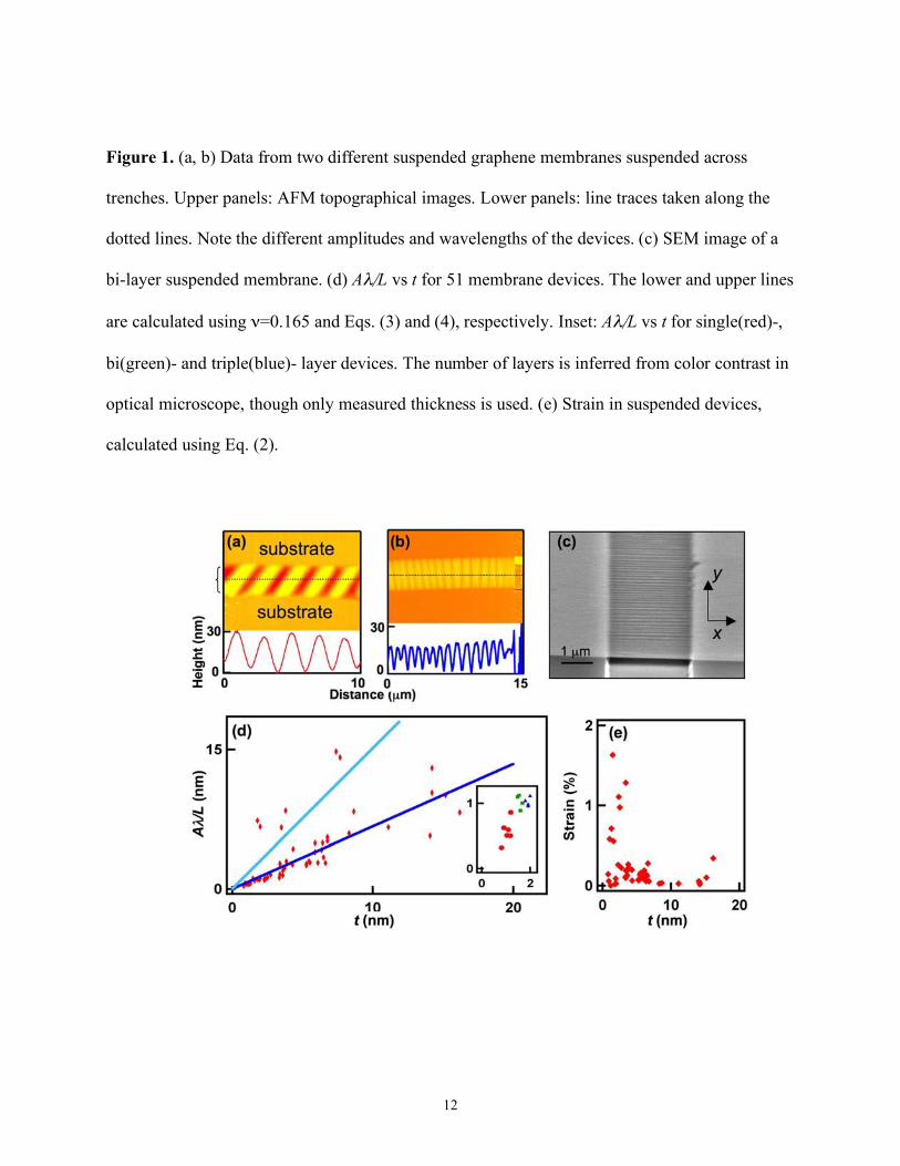
Such interplay between the thermal expansion of the substrate and the membrane suggest
a simple way to control both the amplitude (or, if desired, the wavelength) and orientation of the
ripples. Since the membranes buckle readily under compression, the transverse compressive
strain[18] is
!
" ~ 1+# 2
$2%1. Hence A and λ of the post-annealed wrinkles are related,
!
A ~ " # for A<<λ. Since Δ arises from the difference in TEC between the substrate and
graphene, we expect Δ to scale with Θmax, the maximum annealing temperature rise above
ambient. Fig. 3a plots A vs
!
" #max
for 6 different devices, each thermally cycled to several
different temperatures. Indeed, the data points fall approximately on a straight line. Thus, for a
given set of boundary conditions, the ripple’s A and λ can be controlled by Θmax.
To control the orientation of the ripples, we note that the ripple patterns are determined
by the substrate-imposed boundary conditions (e.g. buckling vs. rippling in x and y-directions,
respectively). This is similar to that in metallic thin films on elastomeric substrates that were
patterned with relief structures[23]. In both experiments, ripples patterns, in which crests are
aligned perpendicular to the step-like structures on the substrate, arise from the redistribution of
compressive stresses due to the TEC differential between the substrate and thin film. Hence, as
the first step towards controlled creation of 2D ripples, we pattern openings of different shapes
on the substrates. Graphene membranes are suspended over these openings; annealing in
temperature up to 700K yields striking patterns of 2D ripples, with the crests perpendicular to the
edges of the opening (Fig. 3b). Such 1D or 2D ripple patterns may be desirable for novel devices
Page 7
7
such as in-plane electronic superlattices[24, 25]. In the long term, just as the creation of complex
patterns was demonstrated in ref.[23], simple thermal manipulation, coupled with pre-patterned
relief structures on substrates, can be used to engineer graphene’s local morphology and alter its
electronic properties. Such processes are also compatible with large-scale device applications.
We now explore the interplay between the ripple mechanics and graphene’s
thermodynamical and electrical properties. Notably, our thermo-mechanical control of the
amplitude and orientation of the ripples proves to be exceedingly effective, due to graphene’s
negative TEC that accentuates the TEC-difference between the substrate and graphene. Indeed, a
negative TEC is expected as a consequence of graphene’s two-dimensionality, in which the
energies of out-of-plane (bending) phonon modes is lower for smaller lattice parameters[26].
However, although graphene’s TEC has been calculated[27-29], no experimental measurement
has been reported to date.
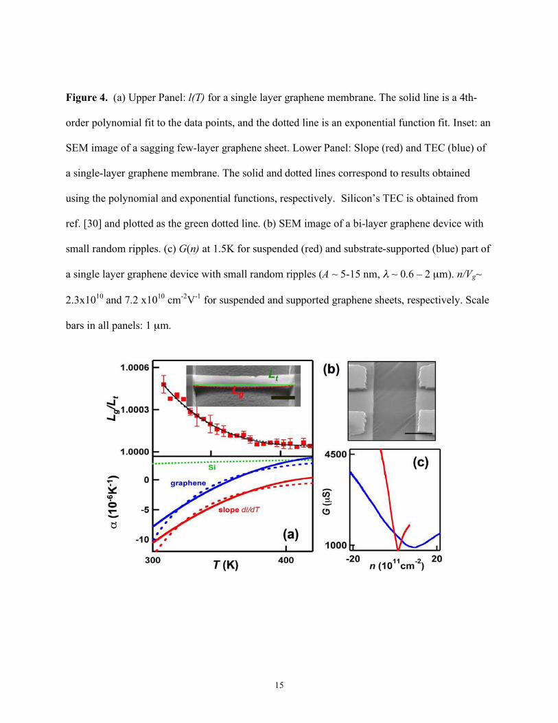
Our experiment readily enables measurement of the TEC α(Τ). To this end, we anneal a
single-layer graphene sheet in a furnace up to 700K to create a sagging membrane. This device is
then inserted into the SEM chamber, and heated up to ~450 K, at which the membrane is taut
across the trench. The heater is then turned off to allow the membrane to cool to 300K. At a
given temperature T, we take an image of the sagging membrane, and compute the ratio
l(T)=Lg(T)/Lt(T), where Lg is the length of graphene membrane as measured along the arc, and Lt
is the length of the trench measured along the chord of the arc (Fig. 4a inset). Both quantities are
measured independently for every image to minimize errors induced by, e.g., slight variations in
the imaging conditions. In Fig. 4a we plot l(T) for a single layer graphene sheet. The slope of the
graph can be approximated by
!
b =dl
dT"# $#
Si, where αSi is silicon’s TEC. To obtain b, the data
points are approximated by an analytical function, which is then differentiated. Two different
Page 8
8
fitting functions are used to illustrate the error range of this procedure. Using values of αSi(T)
from ref. [30], we can determine α(Τ) for graphene (lower panel of Fig. 4a, blue lines). Our
measurements indicate that at 300K, α~−7x10⁻⁶ K-1. This agrees with our expectation that α is
much larger than that of graphite in the basal plane, ~ −1x10⁻⁶ K-1. However, the measured α is
roughly twice the value predicted from theoretical calculation, and approaches zero more quickly
than expected[27]. Part of the discrepancy may be attributed to our unconventional method to
determine α; nevertheless, this first quantitative measurement of graphene’s TEC provides
important insight into graphene’s unique thermal properties.
Finally, we note that our ability to controllably create ripples in graphene opens a door
for systematic investigation of ripples’ effects on graphene’s electrical properties, and strain-
based engineering of graphene devices. For instance, despite intense theoretical interest[8, 31-
34], the nature and magnitude of ripples’ effects on electron scattering processes have not been
experimentally studied, and remain controversial to date. As an initial demonstration of such
studies, we fabricate suspended graphene devices with two electrodes on each side of the trench
(Fig. 4b), allowing measurements of both suspended and substrate-supported portions of the
same graphene sheet. Fig. 4c shows the 2-probe conductance G of a single layer graphene device
with small random ripples as a function of the charge density n. Comparing with the substrate-
supported part, the suspended part of graphene has much higher mobility, with a sharper Dirac
point that is closer to n=0, indicating smaller density of charged impurities. Thus, our
measurements confirm that, despite the presence of small random ripples, the device mobility is
substantially enhanced by the elimination of the substrate. This is consistent with prior results
from high-mobility suspended graphene devices[15, 16], which, in light of our results, are also
likely to contain ripples. Our observation of the temperature-dependent morphology of
Page 9
9
suspended graphene sheets may also have implications on understanding results reported in ref.
[16], in which suspended graphene devices display unusual G(T) behaviors with large sample-to-
sample variations.
We thank Marc Bockrath and Shan-Wen Tsai for discussions, and Bophan Chim, Dong
Yan and Zeng Zhao for assistance with SEM imaging. This research is supported in part by
NSF/CAREER DMR/0748910, NSF/CBET 0756359 and ONR/DMEA H94003-07-2-0703.
Page 10
10
References
[1] K. S. Novoselov et al., Nature 438, 197 (2005).
[2] Y. B. Zhang, Y. W. Tan, H. L. Stormer, and P. Kim, Nature 438, 201 (2005).
[3] F. Miao et al., Science 317, 1530 (2007).
[4] J. S. Bunch et al., Science 315, 490 (2007).
[5] C. Lee, X. D. Wei, J. W. Kysar, and J. Hone, Science 321, 385 (2008).
[6] J. C. Meyer et al., Nature 446, 60 (2007).
[7] F. Guinea, B. Horovitz, and P. Le Doussal, Phys. Rev. B 77, 205421 (2008).
[8] F. Guinea, M. I. Katsnelson, and M. A. H. Vozmediano, Phys. Rev. B 77, 075422 (2008).
[9] A. L. V. de Parga et al., Phys. Rev. Lett. 100, 056807 (2008).
[10] E.-A. Kim and A. H. Castro Neto, Europhys. Lett. 84, 57007 (2008).
[11] M. I. Katsnelson and A. K. Geim, Phil. Trans. Roy. Soc. A 366, 195 (2008).
[12] S. V. Morozov et al., Phys. Rev. Lett. 100, 016602 (2008).
[13] V. M. Pereira and A. H. Castro Neto, arXiv:0810.4539v1 (2008).
[14] D. C. Elias et al., arXiv:0810.4706v1 (2008).
[15] X. Du, I. Skachko, A. Barker, and E. Y. Andrei, Nature Nanotechnol. 3, 491 (2008).
[16] K. I. Bolotin et al, Phys. Rev. Lett. 101, 096802 (2008).
[17] Supplementary material. [18] E. Cerda and L. Mahadevan, Phys. Rev. Lett. 90, 074302 (2003).
[19] E. M. Lifshitz and L. D. Landau, Theory of Elasticity (Butterworth-Heinemann, London,
1959), 3rd ed.
[20] O. L. Blakslee et al, J. Appl. Phys. 41, 3373 (1970).
[21] Y. W. Wong, S. Pellegrino, and J. Mechan. Mater. Struct. 1, 25 (2006).
Page 11
11
[22] P. Peyla, Eur. Phys. J. B 48, 379 (2005).
[23] N. Bowden et al, Nature 393, 146 (1998).
[24] A. Isacsson, L. M. Jonsson, J. M. Kinaret, and M. Jonson, Phys. Rev. B 77, 035423
(2008).
[25] C. H. Park et al, Nano Lett. 8, 2920 (2008).
[26] M. E. Simon and C. M. Varma, Phys. Rev. Lett. 86, 1781 (2001).
[27] N. Mounet and N. Marzari, Phys. Rev. B 71, 205214 (2005).
[28] Y. K. Kwon, S. Berber, and D. Tomanek, Phys. Rev. Lett. 92, 015901 (2004).
[29] P. K. Schelling and R. Keblinski, Phys. Rev. B 68, 035425 (2003).
[30] H. Watanabe, N. Yamada, and M. Okaji, Int. J. Thermophys. 25, 221 (2004).
[31] T. O. Wehling et al, Europhys. Lett. 84, 17003 (2008).
[32] I. F. Herbut, V. Juricic, and O. Vafek, Phys. Rev. Lett. 100, 046403 (2008).
[33] L. Brey and J. J. Palacios, Phys. Rev. B 77, 041403 (2008).
[34] F. de Juan, A. Cortijo, and M. A. H. Vozmediano, Phys. Rev. B 76, 165409 (2007).
Page 12
12
Figure 1. (a, b) Data from two different suspended graphene membranes suspended across
trenches. Upper panels: AFM topographical images. Lower panels: line traces taken along the
dotted lines. Note the different amplitudes and wavelengths of the devices. (c) SEM image of a
bi-layer suspended membrane. (d) Aλ/L vs t for 51 membrane devices. The lower and upper lines
are calculated using ν=0.165 and Eqs. (3) and (4), respectively. Inset: Aλ/L vs t for single(red)-,
bi(green)- and triple(blue)- layer devices. The number of layers is inferred from color contrast in
optical microscope, though only measured thickness is used. (e) Strain in suspended devices,
calculated using Eq. (2).
Page 13
13
Figure 2. Graphene membranes before (left panels), during (middle) and after (right) annealing.
(a, b) In situ SEM images of two devices. Bottom panels of (b) are higher magnification images
of the edge of the graphene membrane, which sags into the trench after annealing. (c) Schematic
of buckling of a graphene membrane. The arrows indicate the contraction/expansion of the
substrate and graphene.
Page 14
14
Figure 3. (a) A vs. λΘmax1/2 for post-annealed devices. (b) Formation of periodic 2D ripples in
graphene membranes suspended over openings of various shapes. Scale bars: 1 µm.
Page 15
15
Figure 4. (a) Upper Panel: l(T) for a single layer graphene membrane. The solid line is a 4th-
order polynomial fit to the data points, and the dotted line is an exponential function fit. Inset: an
SEM image of a sagging few-layer graphene sheet. Lower Panel: Slope (red) and TEC (blue) of
a single-layer graphene membrane. The solid and dotted lines correspond to results obtained
using the polynomial and exponential functions, respectively. Silicon’s TEC is obtained from
ref. [30] and plotted as the green dotted line. (b) SEM image of a bi-layer graphene device with
small random ripples. (c) G(n) at 1.5K for suspended (red) and substrate-supported (blue) part of
a single layer graphene device with small random ripples (A ~ 5-15 nm, λ ~ 0.6 – 2 µm). n/Vg~
2.3x10¹⁰ and 7.2 x1010 cm-2V-1 for suspended and supported graphene sheets, respectively. Scale
bars in all panels: 1 µm.