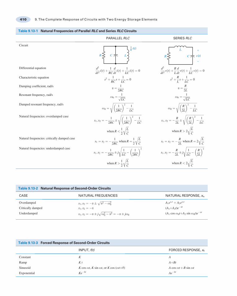
Table 9.13-1 Natural Frequencies of Parallel RLC and Series RLC Circuits PARALLEL RLC SERIES RLC Circuit L R C i(t) L C R v(t) + – Differential equation d 2 dt 2 it ðÞþ 1 RC d dt it ðÞþ 1 LC it ðÞ¼ 0 d 2 dt 2 vt ðÞþ R L d dt vt ðÞþ 1 LC vt ðÞ¼ 0 Characteristic equation s 2 þ 1 RC s þ 1 LC ¼ 0 s 2 þ R L s þ 1 LC ¼ 0 Damping coefficient, rad/s a ¼ 1 2RC a ¼ R 2L Resonant frequency, rad/s o 0 ¼ 1 ffiffiffiffiffiffi LC p o 0 ¼ 1 ffiffiffiffiffiffi LC p Damped resonant frequency, rad/s o d ¼ ffiffiffiffiffiffiffiffiffiffiffiffiffiffiffiffiffiffiffiffiffiffiffiffiffiffiffiffiffiffi 1 2RC 2 1 LC s o d ¼ ffiffiffiffiffiffiffiffiffiffiffiffiffiffiffiffiffiffiffiffiffiffiffiffiffiffi R 2L 2 1 LC s Natural frequencies: overdamped case s 1 ; s 2 ¼ 1 2RC ffiffiffiffiffiffiffiffiffiffiffiffiffiffiffiffiffiffiffiffiffiffiffiffiffiffiffiffi ffi 1 2RC 2 1 LC s s 1 ; s 2 ¼ R 2L ffiffiffiffiffiffiffiffiffiffiffiffiffiffiffiffiffiffiffiffiffiffiffiffiffiffi R 2L 2 1 LC s when R < 1 2 ffiffiffi L C r when R > 2 ffiffiffi L C r Natural frequencies: critically damped case s 1 ¼ s 2 ¼ 1 2RC when R ¼ 1 2 ffiffiffi L C r s 1 ¼ s 2 ¼ R 2L when R ¼ 2 ffiffiffi L C r Natural frequencies: underdamped case s 1 ; s 2 ¼ 1 2RC j ffiffiffiffiffiffiffiffiffiffiffiffiffiffiffiffiffiffiffiffiffiffiffiffiffiffiffiffi ffi 1 LC 1 2RC 2 s s 1 ; s 2 ¼ R 2L j ffiffiffiffiffiffiffiffiffiffiffiffiffiffiffiffiffiffiffiffiffiffiffiffiffiffi 1 LC R 2L 2 s when R > 1 2 ffiffiffi L C r when R < 2 ffiffiffi L C r Table 9.13-2 Natural Response of Second-Order Circuits CASE NATURAL FREQUENCIES NATURAL RESPONSE, x n Overdamped s 1 ; s 2 ¼a ffiffiffiffiffiffiffiffiffiffiffiffiffiffiffiffi a 2 o 2 0 p A 1 e s1t þ A 2 e s2t Critically damped s 1 ; s 2 ¼a (A 1 þA 2 t)e at Underdamped s 1 ; s 2 ¼a j ffiffiffiffiffiffiffiffiffiffiffiffiffiffiffiffi o 2 0 a 2 p ¼a jo d (A 1 cos o d tþA 2 sin o d t)e at Table 9.13-3 Forced Response of Second-Order Circuits INPUT, f(t) FORCED RESPONSE, x f Constant K A Ramp Kt AþBt Sinusoid K cos ot, K sin ot, or K cos (otþy) A cos ot þ B sin ot Exponential Ke bt Ae bt 410 9. The Complete Response of Circuits with Two Energy Storage Elements
Transcript
Table 9.13-1 Natural Frequencies of Parallel RLC and Series RLC Circuits
Table 9.13-3 Forced Response of Second-Order Circuits
INPUT, f(t) FORCED RESPONSE, xf
Constant K A
Ramp K t AþBt
Sinusoid K cos ot, K sin ot, or K cos (otþy) A cos otþB sin ot
Exponential Ke&bt Ae&bt
410 9. The Complete Response of Circuits with Two Energy Storage Elements
PROBLEMS
Section 9.2 Differential Equation for Circuits withTwo Energy Storage Elements
P 9.2-1 Find the differential equation for the circuit shownin Figure P 9.2-1 using the direct method.
vs 100 Ω
2 Ω
10 F
1 mH
µ+–
Figure P 9.2-1
P 9.2-2 Find the differential equation for the circuit shown inFigure P 9.2-2 using the operator method.
Answer:
d2
dt2 iL tð Þ þ 11; 000ddt
iL tð Þ þ 1:1 ' 108iL tð Þ ¼ 108is tð Þ
is 100 Ω
1 mH
10 Ω
10 Fµ
iL
Figure P 9.2-2
P 9.2-3 Find the differential equation for iL(t) for t > 0 for thecircuit of Figure P 9.2-3.
R1
R2
L
+–
is
vcC
vs
iL
t = 0
+
–
Figure P 9.2-3
P 9.2-4 The input to the circuit shown in Figure P 9.2-4 isthe voltage of the voltage source, Vs. The output is the inductorcurrent i(t). Represent the circuit by a second-order differentialequation that shows how the output of this circuit is related tothe input for t> 0.
Hint: Use the direct method.
R2
L+– Vs
i(t)
t = 0
v(t)
+
–
R1R3
C
Figure P 9.2-4
P 9.2-5 The input to the circuit shown in Figure P 9.2-5 isthe voltage of the voltage source, vs. The output is the capacitorvoltage v(t). Represent the circuit by a second-order differentialequation that shows how the output of this circuit is related tothe input for t > 0.
Hint: Use the direct method.
+– vs
R1
R2
L
i(t)
v(t)
+
–
C
t = 0
Figure P 9.2-5
P 9.2-6 The input to the circuit shown in Figure P 9.2-6 is thevoltage of the voltage source, vs. The output is the inductorcurrent i(t). Represent the circuit by a second-order differentialequation that shows how the output of this circuit is related tothe input for t > 0.
Hint: Use the direct method.
+– vs
R1
R2
L i(t)
v(t)
+
–
C
t = 0
Figure P 9.2-6
Problem available in WileyPLUS at instructor’s discretion.
Problems 411
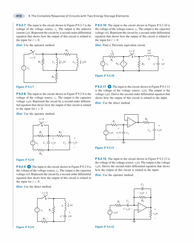
P 9.2-7 The input to the circuit shown in Figure P 9.2-7 is thevoltage of the voltage source, vs. The output is the inductorcurrent i2(t). Represent the circuit by a second-order differentialequation that shows how the output of this circuit is related tothe input for t > 0.
Hint: Use the operator method.
+– vs
R1
R2
L1 i1(t)
t = 0
L2 i2(t)
R3
Figure P 9.2-7
P 9.2-8 The input to the circuit shown in Figure P 9.2-8 is thevoltage of the voltage source, vs. The output is the capacitorvoltage v2(t). Represent the circuit by a second-order differen-tial equation that shows how the output of this circuit is relatedto the input for t > 0.
Hint: Use the operator method.
+– vs
R1 R2
v2(t)
+
–
C2
t = 0
v1(t)
+
–
C1
R3
Figure P 9.2-8
P 9.2-9 The input to the circuit shown in Figure P 9.2-9 isthe voltage of the voltage source, vs. The output is the capacitorvoltage v(t). Represent the circuit by a second-order differentialequation that shows how the output of this circuit is related tothe input for t > 0.
Hint: Use the direct method.
+– vs R1
R2
L i(t)
v(t)+
–C
t = 0
Figure P 9.2-9
P 9.2-10 The input to the circuit shown in Figure P 9.2-10 isthe voltage of the voltage source, vs. The output is the capacitorvoltage v(t). Represent the circuit by a second-order differentialequation that shows how the output of this circuit is related tothe input for t > 0.
Hint: Find a Th!evenin equivalent circuit.
+–
ia
biavs
R1
R2
L
i(t)
v(t)
+
–
C
t = 0
Figure P 9.2-10
P 9.2-11 The input to the circuit shown in Figure P 9.2-11is the voltage of the voltage source, vs(t). The output is thevoltage v2(t). Derive the second-order differential equation thatshows how the output of this circuit is related to the input.
Hint: Use the direct method.
–
+
v2(t)
+
–
C2v1(t)
+
–
C1+–
R1
vs(t)
R2
Figure P 9.2-11
P 9.2-12 The input to the circuit shown in Figure P 9.2-12 isthe voltage of the voltage source, vs(t). The output is the voltagevo(t). Derive the second-order differential equation that showshow the output of this circuit is related to the input.
Hint: Use the operator method.
+
–
+–
v2(t) +–
C2
R2
v1(t)+ –
C1R1
vo(t)
+
–
vs(t)
Figure P 9.2-12
412 9. The Complete Response of Circuits with Two Energy Storage Elements
P 9.2-13 The input to the circuit shown in Figure P 9.2-13is the voltage of the voltage source, vs(t). The output is thevoltage vo(t). Derive the second-order differential equation thatshows how the output of this circuit is related to the input.
Hint: Use the direct method.
+
–
+–
v(t) +–
C
R2
R1
vo(t)
+
–
vs(t)
t = 0
L
i(t)
Figure P 9.2-13
P 9.2-14 The input to the circuit shown in Figure P 9.2-14 isthe voltage of the voltage source, vs(t). The output is the voltagev2(t). Derive the second-order differential equation that showshow the output of this circuit is related to the input.
Hint: Use the direct method.
+
–
+–
v1(t)+ –
C1
R2
R1
vs(t)
R3
v2(t)
+
–
C2
Figure P 9.2-14
P 9.2-15 Find the second-order differential equation for i2for the circuit of Figure P 9.2-15 using the operator method.Recall that the operator for the integral is 1=s.
Answer: 3d2i2dt2 þ 4
di2dt
þ 2 i2 ¼ d2vs
dt2
i1 i2vs1 H
+– 1 2
1 Ω 2 Ω
F
Figure P 9.2-15
Section 9.3 Solution of the Second-OrderDifferential Equation—The Natural ResponseP 9.3-1 Find the characteristic equation and its roots for thecircuit of Figure P 9.2-2.
P 9.3-2 Find the characteristic equation and its roots for thecircuit of Figure P 9.3-2.
P 9.3-3 Find the characteristic equation and its roots for thecircuit shown in Figure P 9.3-3.
vs 1 mH
2 Ω1 Ω
10 Fµ+–
vc
iL
+
–
Figure P 9.3-3
P 9.3-4 German automaker Volkswagen, in its bid to makemore efficient cars, has come up with an auto whose enginesaves energy by shutting itself off at stoplights. The stop–startsystem springs from a campaign to develop cars in all its worldmarkets that use less fuel and pollute less than vehicles now onthe road. The stop–start transmission control has a mechanismthat senses when the car does not need fuel: coasting downhilland idling at an intersection. The engine shuts off, but a smallstarter flywheel keeps turning so that power can be quicklyrestored when the driver touches the accelerator.
A model of the stop–start circuit is shown in FigureP 9.3-4. Determine the characteristic equation and the naturalfrequencies for the circuit.
Answer: s2 þ 20s þ 400 ¼ 0s ¼ &10 ( j17:3
1 2 H
10 Ω
+–
+–
5 mF
10u(t) V
7u(t) V
Figure P 9.3-4 Stop–start circuit.
Problems 413
Section 9.4 Natural Response of the UnforcedParallel RLC Circuit
P 9.4-1 Determine v(t) for the circuit of Figure P 9.4-1 when L¼ 1 H and vs ¼ 0 for t , 0. The initial conditions are v(0) ¼ 6 Vand dv=dt(0) ¼ &3000 V/s.
Answer: v tð Þ ¼ &2e&100t þ 8e&400t V
L
Ω80+
–v(t) 25 Fµ+
–vs(t)
Figure P 9.4-1
P 9.4-2 An RLC circuit is shown in Figure P 9.4-2, inwhich v(0) ¼ 2 V. The switch has been open for a long timebefore closing at t ¼ 0. Determine and plot v(t).
F 1 HΩt = 0
v(t)+
–3 41 3
Figure P 9.4-2
P 9.4-3 Determine i1(t) and i2(t) for the circuit of FigureP 9.4-3 when i1(0) ¼ i2(0) ¼ 11 A.
i2Ω2
i1
2 H
3 HΩ1
Figure P 9.4-3
P 9.4-4 The circuit shown in Figure P 9.4-4 contains a switchthat is sometimes open and sometimes closed. Determine thedamping factor a, the resonant frequency o0, and the dampedresonant frequency od of the circuit when (a) the switch is openand (b) the switch is closed.
+–
i(t)
v(t)
+
–
5 mF50 Ω
10 Ω
2 H
20 V
40 Ω
Figure P 9.4-4
P 9.4-5 The circuit shown in Figure P 9.4-5 is used in air-planes to detect smokers who surreptitiously light up beforethey can take a single puff. The sensor activates the switch, and
the change in the voltage v(t) activates a light at the flightattendant’s station. Determine the natural response v(t).
Answer: v tð Þ ¼ &1:16e&2:7t þ 1:16e&37:3t V
1 A1 Ω
0.4 H F v(t)+
–
Light bulb
t = 01 40
Sensor
Figure P 9.4-5 Smoke detector.
Section 9.5 Natural Response of the CriticallyDamped Unforced Parallel RLC Circuit
P 9.5-1 Find vc(t) for t > 0 for the circuit shown in FigureP 9.5-1.
Answer: vc tð Þ ¼ 3 þ 6000tð Þe&2000t V
100 Ω 30u(–t) mA
25 mH
10 mFvc+–
Figure P 9.5-1
P 9.5-2 Find vc(t) for t > 0 for the circuit of Figure P 9.5-2.Assume steady-state conditions exist at t ¼ 0&.
Answer: vc tð Þ ¼ &8te&2t V
+–
t = 0
20 V F vc+
–11
Ω10
1 4H Ω
Figure P 9.5-2
P 9.5-3 Police often use stun guns to incapacitate potentiallydangerous felons. The handheld device provides a series ofhigh-voltage, low-current pulses. The power of the pulses is farbelow lethal levels, but it is enough to cause muscles to contractand put the person out of action. The device provides a pulse ofup to 50,000 V, and a current of 1 mA flows through an arc.A model of the circuit for one period is shown in Figure P 9.5-3.Find v(t) for 0 < t < 1 ms. The resistor R represents the sparkgap. Select C so that the response is critically damped.
+– v
+
–R = 106 Ω
t = 0 104 V
10 mH
C
Figure P 9.5-3
414 9. The Complete Response of Circuits with Two Energy Storage Elements
P 9.5-4 Reconsider Problem P 9.4-1 when L ¼ 640 mH andthe other parameters and conditions remain the same.
Answer: v tð Þ ¼ 6 & 1500tð Þe&250t V
P 9.5-5 An automobile ignition uses an electromagnetic trigger.The RLC trigger circuit shown in Figure P 9.5-5 has a step inputof 6 V, and v(0) ¼ 2 V and i(0) ¼ 0. The resistance R must beselected from 2V<R< 7V so that the current i(t) exceeds 0.6 Afor greater than 0.5 s to activate the trigger. A critically dampedresponse i(t) is required to avoid oscillations in the triggercurrent. Select R and determine and plot i(t).
i6 u(t) Vv(t)
+
+
–
–Trigger
1 H 1 4 F
R
Figure P 9.5-5
Section 9.6 Natural Response of an UnderdampedUnforced Parallel RLC Circuit
P 9.6-1 A communication system from a space station usesshort pulses to control a robot operating in space. The transmittercircuit is modeled in Figure P 9.6-1. Find the output voltage vc(t)for t > 0. Assume steady-state conditions at t ¼ 0&.
Answer: vc tð Þ ¼ e&400t 3 cos 300t þ 4 sin 300t½ * V
+–
vc+
–
6 V
0.8 H
250 Ω
250 Ωt = 0
5 × 10⁻⁶ F
Figure P 9.6-1
P 9.6-2 The switch of the circuit shown in Figure P 9.6-2 isopened at t ¼ 0. Determine and plot v(t) when C ¼ 1=4 F.Assume steady state at t ¼ 0&.
Answer: v tð Þ ¼ &4e&2t sin 2t V
+–
t = 0
6 V C v(t)+
–HΩ1
Ω3
1 2
Figure P 9.6-2
P 9.6-3 A 240-W power supply circuit is shown in FigureP 9.6-3a. This circuit employs a large inductor and a largecapacitor. The model of the circuit is shown in Figure P 9.6-3b.Find iL(t) for t > 0 for the circuit of Figure P 9.6-3b. Assumesteady-state conditions exist at t ¼ 0&.
Answer: iL tð Þ ¼ e&2t &4 cos t þ 2 sin tð Þ A
(a)
2 Ω
4 Ω
8 Ω
iL
1 4 F
7 A
t = 0
4 H
(b)
Figure P 9.6-3 (a) A power supply. (b) Model of the powersupply circuit.
P 9.6-4 The natural response of a parallel RLC circuit ismeasured and plotted as shown in Figure P 9.6-4. Using thischart, determine an expression for v(t).
Hint: Notice that v(t) ¼ 260 mV at t ¼ 5 ms and that v(t) ¼&200 mV at t ¼ 7.5 ms. Also, notice that the time between thefirst and third zero-crossings is 5 ms.
Answer: v tð Þ ¼ 544e&276t sin 1257t V
0 5 10 15 20 25 30–400
–300
–200
–100
0
100
200
300
400
500
600
v(t)(mV)
Time (ms)
Figure P 9.6-4 The natural response of a parallel RLC circuit.
# Courtesy of R.S.R. Electronics, Inc.
Problems 415
P 9.6-5 The photovoltaic cells of the proposed space stationshown in Figure P 9.6-5a provide the voltage v(t) of the circuitshown in Figure P 9.6-5b. The space station passes behind theshadow of earth (at t ¼ 0) with v(0) ¼ 2 V and i(0) ¼ 1/10 A.Determine and sketch v(t) for t > 0.
Photocells
(a)
+
–Ω5
Spacestation
electric motors
2 H F v
The photovoltaiccells connected
in parallel
i
(b)
1 10
Figure P 9.6-5 (a) Photocells on space station. (b) Circuit withphotocells.
Section 9.7 Forced Response of an RLC Circuit
P 9.7-1 Determine the forced response for the inductor currentif when (a) is ¼ 1 A, (b) is ¼ 0.5t A, and (c) is ¼ 2e&250t A for thecircuit of Figure P 9.7-1.
is u(t) A
i
Ω 10 mH 1 mF100 65
Figure P 9.7-1
P 9.7-2 Determine the forced response for the capacitorvoltage vf for the circuit of Figure P 9.7-2 when (a) vs ¼ 2 V,(b) vs ¼ 0.2t V, and (c) vs ¼ 1e&30t V.
+–vs u(t) V v
+
–
7 Ω
833.3 F
0.1 H
µ
Figure P 9.7-2
P 9.7-3 A circuit is described for t > 0 by the equation
d2vdt2
þ 5dvdt
þ 6v ¼ vs
Find the forced response vf for t > 0 when (a) vs ¼ 8 V, (b) vs ¼3e&4t V, and (c) vs ¼ 2e&2t V.
Answer: (a) vf ¼ 8=6 V (b) vf ¼32
e&4t V (c) vf ¼ 2te&2t V
Section 9.8 Complete Response of an RLC Circuit
P 9.8-1 Determine i(t) for t > 0 for the circuit shown in FigureP 9.8-1.
iLi
+–11 mA
t = 01 kΩ 4 V
6.25 H2 kΩ1 µFvc
+
–
Figure P 9.8-1
P 9.8-2 Determine i(t) for t > 0 for the circuit shown in FigureP 9.8-2.
Hint: Show that 1 ¼ d2
dt2 i tð Þ þ 5ddt
i tð Þ þ 5i tð Þ for t > 0
Answer: i tð Þ ¼ 0:2 þ 0:246 e&3:62t & 0:646 e&1:38t A for t > 0.
i(t)2u(t) – 1 V 0.25 Fv(t)+
–
+– 4 H
4 Ω1 Ω
Figure P 9.8-2
P 9.8-3 Determine v1(t) for t > 0 for the circuit shown inFigure P 9.8-3.
Answer: v1 tð Þ ¼ 10 þ e&2:4'104 t & 6 e&4'103 t V for t > 0
+–10 V v1(t)
t = 0+
–
1 kΩ 1 kΩ
1/6 µF v2(t)+
–1/16 µF
Figure P 9.8-3
P 9.8-4 Find v(t) for t > 0 for the circuit shown in FigureP 9.8-4 when v(0) ¼ 1 V and iL(0) ¼ 0.
416 9. The Complete Response of Circuits with Two Energy Storage Elements
Answer: v ¼ 25e&3t & 117
[429e&4t & 21 cos t þ 33 sin t* V
1 12 FiL
+– v
+
–0.5 H5 cos t V
1 Ω 1 Ω
Figure P 9.8-4
P 9.8-5 Find v(t) for t > 0 for the circuit of Figure P 9.8-5.
P 9.8-6 An experimental space station power supply systemis modeled by the circuit shown in Figure P 9.8-6. Find v(t) fort > 0. Assume steady-state conditions at t ¼ 0&.
t = 0
0.125 F+
–4 Ω2 Ω 5 V
4 H
(10 cos t)u(t) V
i(t)
v(t) +–
– +
Figure P 9.8-6
P 9.8-7 Find vc(t) for t > 0 in the circuit of Figure P 9.8-7when (a) C ¼ 1=18 F, (b) C ¼ 1=10 F, and (c) C ¼ 1=20 F.
Answers:
(a) vc tð Þ ¼ 8e&3t þ 24te&3t & 8 V(b) vc tð Þ ¼ 10e&t & 2e&5t & 8 V(c) vc tð Þ ¼ e&3t 8 cos t þ 24 sin tð Þ & 8 V
v(t)+
–4 Ω C
8 Ω
2 H
a
2u(t) A
i(t)
Figure P 9.8-7
P 9.8-8 Find vc(t) for t > 0 for the circuit shown in FigureP 9.8-8.
Hint: 2 ¼ d2
dt2 vc tð Þ þ 6ddt
vc tð Þ þ 2vc tð Þ for t > 0
Answer: vc tð Þ ¼ 0:123e&5:65t þ 0:877e&0:35t þ 1 V for t > 0.
4 Ω 8 Ω
F vC(t)
+
–iL(t)
2 H
u(t) + A– 1 4
1 4
1 2
Figure P 9.8-8
P 9.8-9 In Figure P 9.8-9, determine the inductor currenti(t) when is ¼ 5u(t) A. Assume that i(0) ¼ 0, vc(0) ¼ 0.
Answer: i(t) ¼ 5 + e&2t [&5 cos 5t & 2 sin 5t] A
i
Ω2 Fis8 29 1 8
H
Figure P 9.8-9
P 9.8-10 Railroads widely use automatic identification ofrailcars. When a train passes a tracking station, a wheeldetector activates a radio-frequency module. The module’santenna, as shown in Figure P 9.8-10a, transmits and receivesa signal that bounces off a transponder on the locomotive. A
Vehicle-mountedtransponder tag
Wheel detectorinput
Antenna
+ –
ΩΩ1
L
v
0.5Ω1.5
is
0.5 F
i
(b)
(a)
Figure P 9.8-10 (a) Railroad identification system.(b) Transponder circuit.
Problems 417
trackside processor turns the received signal into useful infor-mation consisting of the train’s location, speed, and directionof travel. The railroad uses this information to schedulelocomotives, trains, crews, and equipment more efficiently.
One proposed transponder circuit is shown in FigureP 9.8-10b with a large transponder coil of L ¼ 5 H. Determinei(t) and v(t). The received signal is is ¼ 9 þ 3e&2t u(t) A.
P 9.8-11 Determine v(t) for t > 0 for the circuit shown inFigure P 9.8-11.
Answer: vc tð Þ ¼ 0:75 e&4t & 6:75 e&36t þ 16 V for t > 0
i(t) va(t)
v(t)
–
+
+
–
4 Ω0.1 H+– 0.625 F
2va(t)6u(t) + 10 V
Figure P 9.8-11
P 9.8-12 The circuit shown in Figure P 9.8-12 is at steady statebefore the switch opens. The inductor current is given to be
i(t) ¼ 240þ 193e&6:25t cos (9:27t & 1021) mA for t , 0
Determine the values of R1, R3, C, and L.
L+–
i(t)
t = 0
v(t)
+
–
R1R3
C 20 Ω
24 V
Figure P 9.8-12
P 9.8-13 The circuit shown in Figure P 9.8-13 is at steadystate before the switch opens. Determine the inductor currenti(t) for t > 0.
+–
i(t)
t = 0
v(t)
+
–
12 Ω
18 V
8 Ω 24 Ω
0.4 H
25 mF
Figure P 9.8-13
*P 9.8-14 The circuit shown in Figure P 9.8-14 is atsteady state before the switch closes. Determine the capacitorvoltage v(t) for t > 0.
+–
ia
3ia
i(t)
v(t)
+
–
t = 0
10 Ω10 Ω20 V
0.4 H
25 mF
Figure P 9.8-14
P 9.8-15 The circuit shown in Figure P 9.8-15 is at steadystate before the switch closes. Determine the capacitor voltage,v(t), for t > 0.
+–
i(t)
v(t)
+
–
t = 0
5 mF50 Ω
50 Ω
2 H
20 V
Figure P 9.8-15
P 9.8-16 The circuit shown in Figure P 9.8-16 is at steadystate before the switch closes. Determine the inductor currenti(t) for t > 0.
+–
i(t)
v(t)
+
–
t = 0
9 Ω
16 Ω
0.4 H
25 mF20 V
Figure P 9.8-16
P 9.8-17 The circuit shown in Figure P 9.8-17 is at steadystate before the switch opens. Determine the inductor currenti2(t) for t > 0.
+–
i1(t)
t = 0
i2(t)24 Ω
75 Ω
15 Ω
4 H 1.6 H
20 V
Figure P 9.8-17
418 9. The Complete Response of Circuits with Two Energy Storage Elements
P 9.8-18 The circuit shown in Figure P 9.8-18 is at steadystate before the switch closes. Determine the capacitor voltagev(t) for t > 0.
+–
i(t)
v(t)
+
–
t = 0
50 Ω
50 Ω
5 mF
2 H
20 V
Figure P 9.8-18
P 9.8-19 Find the differential equation for vc(t) in thecircuit of Figure P 9.8-19, using the direct method. Findvc(t) for time t > 0 for each of the following sets of componentvalues:
(a) C ¼ 1 F, L ¼ 0.25 H, R1 ¼ R2 ¼ 1.309 V(b) C ¼ 1 F, L ¼ 1 H, R1 ¼ 3 V, R2 ¼ 1 V(c) C ¼ 0.125 F, L ¼ 0.5 H, R1 ¼ 1 V, R2 ¼ 4 V
Answer:
(a) vc tð Þ ¼ 12&e&2t þ 1
2e&4t V
(b) vc tð Þ ¼ 14& 1
4þ 1
2t
$ %e&2t V
(c) vc tð Þ ¼ 0:8 & e&2t 0:8 cosð 4t þ 0:4 sin 4tÞ V
L
R2
R1
C+–
iL(t)
vc(t)vs(t) = u(t)+
–
Figure P 9.8-19
P 9.8-20 Find the differential equation for vo(t) in thecircuit of Figure P 9.8-20, using the direct method. Findvo(t) for time t > 0 for each of the following sets of componentvalues:
(a) C ¼ 1 F, L ¼ 0.25 H, R1 ¼ R2 ¼ 1.309 V(b) C ¼ 1 F, L ¼ 1 H, R1 ¼ 1 V, R2 ¼ 3 V(c) C ¼ 0.125 F, L ¼ 0.5 H, R1 ¼ 4 V, R2 ¼ 1 V
Answer:
(a) vo tð Þ ¼ 12& e&2t þ 1
2e&4t V
(b) vo tð Þ ¼ 34& 3
4þ 3
2t
$ %e&2t V
(c) vo tð Þ ¼ 0:2 & e&2t 0:2 cos 4t þ 0:1 sin 4tð Þ V
L
R2
R1
C+–
iL(t)
vo(t)vs(t) = u(t)
+
–
vc(t)+
–
Figure P 9.8-20
Section 9.9 State Variable Approach to CircuitAnalysis
P 9.9-1 Find v(t) for t > 0, using the state variablemethod of Section 9.9 when C ¼ 1=5 F in the circuitof Figure P 9.9-1. Sketch the response for v(t) for 0 <t < 10 s.
Answer: v tð Þ ¼ &25e&t þ e&5t þ 24 V
6 Ω
v+
–C
1 H
4u(t) A
Figure P 9.9-1
P 9.9-2 Repeat Problem P 9.9-1 when C ¼ 1=10 F. Sketch theresponse for v(t) for 0 < t < 3 s.
Answer: v tð Þ ¼ e&3t &24 cos t & 32 sin tð Þ þ 24 V
P 9.9-3 Determine the current i(t) and the voltage v(t) for thecircuit of Figure P 9.9-3.
Answer: i tð Þ ¼ 3:08e&2:57t & 0:08e&97:4t & 6! "
A
0.5 Ωi
–3u(t) A 0.2 H v+
–20 mF 3 A
Figure P 9.9-3
P 9.9-4 Clean-air laws are pushing the auto industrytoward the development of electric cars. One proposedvehicle using an ac motor is shown in Figure P 9.9-4a.The motor-controller circuit is shown in Figure P 9.9-4bwith L ¼ 100 mH and C ¼ 10 mF. Using the state equationapproach, determine i(t) and v(t) where i(t) is the motor-control current. The initial conditions are v(0) ¼ 10 V andi(0) ¼ 0.
Problems 419
P 9.9-5 Studies of an artificial insect are being used to under-stand the nervous system of animals. A model neuron in thenervous system of the artificial insect is shown in Figure P 9.9-5.The input signal vs is used to generate a series of pulses, calledsynapses. The switch generates a pulse by opening at t ¼ 0 andclosing at t ¼ 0.5 s. Assume that the circuit is at steady state andthat v(0&) ¼ 10 V. Determine the voltage v(t) for 0 < t < 2 s.
+– vvs
+
–F30 V
H
3 Ω
6 ΩSwitch
1 6
1 2
Figure P 9.9-5 Neuron circuit model.
Section 9.10 Roots in the Complex Plane
P 9.10-1 For the circuit of Figure P 9.10-1, determinethe roots of the characteristic equation and plot the roots onthe s-plane.
3 kΩ2 kΩ
i1 i2
+– 2 mH2 mH12 – 6u(t) V
Figure P 9.10-1
P 9.10-2 For the circuit of Figure P 9.6-1, determine the rootsof the characteristic equation and plot the roots on the s-plane.
P 9.10-3 For the circuit of Figure P 9.10-3, determine the rootsof the characteristic equation and plot the roots on the s-plane.
vs 4 kΩF
4 H
µ1 4+–
Figure P 9.10-3
P 9.10-4 An RLC circuit is shown in Figure P 9.10-4.
(a) Obtain the two-node voltage equations, using operators.(b) Obtain the characteristic equation for the circuit.(c) Show the location of the roots of the characteristic equation
in the s-plane.(d) Determine v(t) for t > 0.
36u(t) V +–
Ω12 Ω6
a b
v(t)+
–F
1 H
1 18
Figure P 9.10-4
Section 9.11 How CanWe Check . . . ?
P 9.11-1 Figure P 9.11-1a shows an RLC circuit. The voltagevs(t) of the voltage source is the square wave shown in FigureP 9.11-1a. Figure P 9.11-1c shows a plot of the inductor currenti(t), which was obtained by simulating this circuit, usingPSpice. Verify that the plot of i(t) is correct.
Answer: The plot is correct.
+ –
Ω2vx
vx
2ix
1
ix
L
2C
v
+
–
i
Ω
+ –
Transistorizeddc to ac inverter
Integrated interiorpermanent magnet
ac motor andautomatic transaxle
Sodium-sulfurbattery
Systemcontroller
Electric powersteering
(a) (b)
Figure P 9.9-4 (a) Electric vehicle. (b) Motor-controller circuit.
420 9. The Complete Response of Circuits with Two Energy Storage Elements
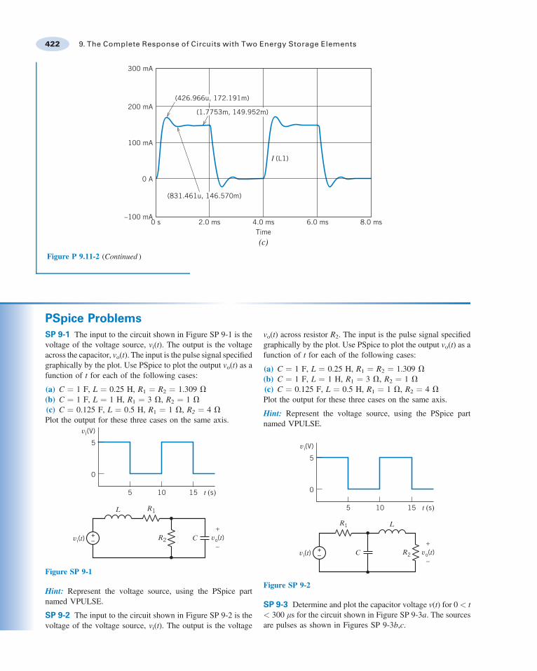
P 9.11-2 Figure P 9.11-2b shows an RLC circuit. Thevoltage vs(t) of the voltage source is the square wave shownin Figure P 9.11-2a. Figure P 9.11-2c shows a plot of
the inductor current i(t), which was obtained by simulatingthis circuit, using PSpice. Verify that the plot of i(t) is correct.
Answer: The plot is not correct.
t, ms
(a)
0
25
4 8 12 16
vs, V
+–
(b)
i(t)100 Ω
12 mHvs µ2 F
(c)
0 A
–200 mA
200 mA
400 mA
0 s 2.0 ms 4.0 ms 6.0 ms 8.0 msTimeI (L1)
I (L1)
(550.562u, 321.886m)
(1.6405m, 256.950m)
(1.0787m, 228.510m)
(3.6854m, 250.035m)
Figure P 9.11-1
t, ms
+–
(b)(a)
i(t)100 Ω
0
15
2 4 6 8
vs, V
8 mHvs µ0.2 F
Figure P 9.11-2
Problems 421
PSpice ProblemsSP 9-1 The input to the circuit shown in Figure SP 9-1 is thevoltage of the voltage source, vi(t). The output is the voltageacross the capacitor, vo(t). The input is the pulse signal specifiedgraphically by the plot. Use PSpice to plot the output vo(t) as afunction of t for each of the following cases:
(a) C ¼ 1 F, L ¼ 0.25 H, R1 ¼ R2 ¼ 1.309 V(b) C ¼ 1 F, L ¼ 1 H, R1 ¼ 3 V, R2 ¼ 1 V(c) C ¼ 0.125 F, L ¼ 0.5 H, R1 ¼ 1 V, R2 ¼ 4 VPlot the output for these three cases on the same axis.
0
5
vi(V)
t (s)10 15
5
vo(t)vi(t) R2
R1L
+
–C+
–
Figure SP 9-1
Hint: Represent the voltage source, using the PSpice partnamed VPULSE.
SP 9-2 The input to the circuit shown in Figure SP 9-2 is thevoltage of the voltage source, vi(t). The output is the voltage
vo(t) across resistor R2. The input is the pulse signal specifiedgraphically by the plot. Use PSpice to plot the output vo(t) as afunction of t for each of the following cases:
(a) C ¼ 1 F, L ¼ 0.25 H, R1 ¼ R2 ¼ 1.309 V(b) C ¼ 1 F, L ¼ 1 H, R1 ¼ 3 V, R2 ¼ 1 V(c) C ¼ 0.125 F, L ¼ 0.5 H, R1 ¼ 1 V, R2 ¼ 4 VPlot the output for these three cases on the same axis.
Hint: Represent the voltage source, using the PSpice partnamed VPULSE.
0
5
vi(V)
t (s)10 15
5
vo(t)vi(t)
R1
+
–C+
– R2
L
Figure SP 9-2
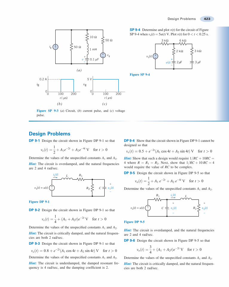
SP 9-3 Determine and plot the capacitor voltage v(t) for 0 < t< 300 ms for the circuit shown in Figure SP 9-3a. The sourcesare pulses as shown in Figures SP 9-3b,c.
(c)
0 A
–100 mA
200 mA
100 mA
300 mA
0 s 2.0 ms 4.0 ms 6.0 ms 8.0 msTime
I (L1)
(426.966u, 172.191m)
(1.7753m, 149.952m)
(831.461u, 146.570m)
Figure P 9.11-2 (Continued )
422 9. The Complete Response of Circuits with Two Energy Storage Elements
v 0.1 Fµ
+–+
–
ig Ω50
Ω50
1 mH
vg
Ω10
(a)
0 100 2000
0.2 A
ig
t ( s)µ0 100 200
0
5 V
vg
t ( s)µ
(b) (c)
Figure SP 9-3 (a) Circuit, (b) current pulse, and (c) voltagepulse.
SP 9-4 Determine and plot v(t) for the circuit of FigureSP 9-4 when vs(t) ¼ 5u(t) V. Plot v(t) for 0 < t < 0.25 s.
+–
v(t)+
–
vs(t)
2 Fµ
Ω3 k Ω6 k
Ω2 k Ω3 k
3 Fµ
Figure SP 9-4
Design ProblemsDP 9-1 Design the circuit shown in Figure DP 9-1 so that
vc tð Þ ¼ 12þ A1e&2t þ A2e&4t V for t > 0
Determine the values of the unspecified constants A1 and A2.
Hint: The circuit is overdamped, and the natural frequenciesare 2 and 4 rad/sec.
L
R2
R1
C+–
iL(t)
vc(t)vs(t) = u(t)+
–
Figure DP 9-1
DP 9-2 Design the circuit shown in Figure DP 9-1 so that
vc tð Þ ¼ 14þ A1 þ A2tð Þe&2t V for t > 0
Determine the values of the unspecified constants A1 and A2.
Hint: The circuit is critically damped, and the natural frequen-cies are both 2 rad/sec.
DP 9-3 Design the circuit shown in Figure DP 9-1 so that
vc tð Þ ¼ 0:8þ e&2t A1 cos 4t þ A2 sin 4tð ÞV for t > 0
Determine the values of the unspecified constants A1 and A2.
Hint: The circuit is underdamped, the damped resonant fre-quency is 4 rad/sec, and the damping coefficient is 2.
DP 9-4 Show that the circuit shown in Figure DP 9-1 cannot bedesigned so that
vc tð Þ ¼ 0:5þ e&2t A1 cos 4t þ A2 sin 4tð ÞV for t > 0
Hint: Show that such a design would require 1=RC þ 10RC ¼4 where R ¼ R1 ¼ R2. Next, show that 1=RC þ 10 RC ¼ 4would require the value of RC to be complex.
DP 9-5 Design the circuit shown in Figure DP 9-5 so that
vo tð Þ ¼ 12þ A1 e&2t þ A2 e&4t V for t > 0
Determine the values of the unspecified constants A1 and A2.
+–
iL(t)
vc(t)
+
–
vo(t)
+
–
L
R2
R1
Cvs(t) = u(t)
Figure DP 9-5
Hint: The circuit is overdamped, and the natural frequenciesare 2 and 4 rad/sec.
DP 9-6 Design the circuit shown in Figure DP 9-5 so that
vo tð Þ ¼ 34þ A1 þ A2tð Þe&2t V for t > 0
Determine the values of the unspecified constants A1 and A2.
Hint: The circuit is critically damped, and the natural frequen-cies are both 2 rad/sec.
Design Problems 423
DP 9-7 Design the circuit shown in Figure DP 9-5 so that
vc tð Þ ¼ 0:2þ e&2t A1 cos 4t þ A2 sin 4tð ÞV for t > 0
Determine the values of the unspecified constants A1 and A2.
Hint: The circuit is underdamped, the damped resonant fre-quency is 4 rad/sec, and the damping coefficient is 2.
DP 9-8 Show that the circuit shown in Figure DP 9-5 cannot bedesigned so that
vc tð Þ ¼ 0:5þ e&2t A1 cos 4t þ A2 sin 4tð ÞV for t > 0
Hint: Show that such a design would require 1=RC þ 10 RC ¼4 where R ¼ R1 ¼ R2. Next, show that 1=RC þ 10 RC ¼ 4would require the value of RC to be complex.
DP 9-9 A fluorescent light uses cathodes (coiled tungstenfilaments coated with an electron-emitting substance) at eachend that send current through mercury vapors sealed in the tube.Ultraviolet radiation is produced as electrons from the cathodesknock mercury electrons out of their natural orbits. Some of thedisplaced electrons settle back into orbit, throwing off the excessenergy absorbed in the collision. Almost all of this energy is in
the form of ultraviolet radiation. The ultraviolet rays, which areinvisible, strike a phosphor coating on the inside of the tube. Therays energize the electrons in the phosphor atoms, and the atomsemit white light. The conversion of one kind of light into anotheris known as fluorescence.
One form of a fluorescent lamp is represented by the RLCcircuit shown in Figure DP 9-9. Select L so that the current i(t)reaches a maximum at approximately t ¼ 0.5 s. Determine themaximum value of i(t). Assume that the switch was in position 1for a long time before switching to position 2 at t ¼ 0.
Hint: Use PSpice to plot the response for several values of L.
t = 0
10 V +–
1 2
i
L
FΩ4
1 3
Figure DP 9-9 Flourescent lamp circuit.
424 9. The Complete Response of Circuits with Two Energy Storage Elements