20
Robu st Low Powe r VLSI ECE 7502 S2015 Canary SRAM Built in Self Test for SRAM Write V MIN Tracking ECE 7502 Class Final Presentation Arijit Banerjee 21 th Apr 2015
| Date post: | 31-Dec-2015 |
| Category: |
Documents |
| Upload: | osborn-mcgee |
| View: | 224 times |
| Download: | 0 times |

Rob
ust
Low
Power
VLSI
ECE7502S2015
Canary SRAM Built in Self Test for SRAM Write VMIN Tracking
ECE 7502 Class Final Presentation
Arijit Banerjee
21th Apr 2015
Rob
ust
Low
Power
VLSI
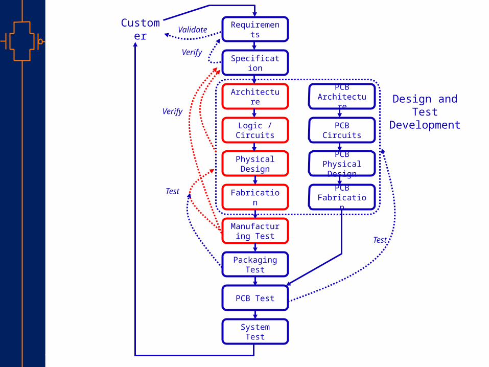
Requirements
Specification
Architecture
Logic / Circuits
Physical Design
Fabrication
Manufacturing Test
Packaging Test
PCB Test
System Test
PCB Architecture
PCB Circuits
PCB Physical Design
PCB Fabrication
Design and Test Development
Customer Validate
Verify
Verify
Test
Test

Rob
ust
Low
Power
VLSI 3
Outline Problem statement: Testing of canary
SRAMs with reverse assist Expected outcomes Approach: proposed canary built in self
test (BIST) Results Conclusions

Rob
ust
Low
Power
VLSI 4
Canary SRAM
An SRAM sensor that can be sensitive to retention, read, write Uses a reverse assist to degrade operations
Canary data retention voltage (DRV) tracking [Wang et al 2007]
Canary write minimum operating voltage (VMIN )tracking [Banerjee et al 2014] Uses BIST to count the # of bit failures User knobs: failure threshold and degree of reverse assist

Rob
ust
Low
Power
VLSI 5
Problem Statement: Testing of Canary SRAMs with Reverse Assist Challenges in testing of canary SRAM
Need to test canaries for a specific trend for bit failure vs. canary reverse assist at speed
Testing should provide production go no-go and diagnostic data of the canaries
Also the CBIST should have some testing capability of itself
How to check the functionality of the canary SRAM with reverse assist so that it can be used to track SRAM write VMIN?
To develop a BIST that can test the failure trends in canary at speed in production run and also provide the failure diagnostic data for the canary SRAM

Rob
ust
Low
Power
VLSI 6
Expected Outcomes To design a CBIST in Verilog and synthesize it in IBM
130nm technology for a 512bit canary with reverse assist To check the trend to be within a max and min (bit failure rate) BFR limit and
monotonicity of the failure data To run at speed covering all the reverse assist settings for write 0 and write 1
trends Will have go no-go production CBIST run support and debug functionality of
each reverse assist settings
Equip CBIST with some design for testability (DFT) feature for testing itself and estimate its test and fault coverage Full scan insertion Estimation of fault coverage using stuck at transition fault models

Rob
ust
Low
Power
VLSI 7
Approach: Proposed Canary BIST Architecture
Verilog entry of the CBIST for a 512b canary SRAM consisting of three blocks CBIST finite
state machine (FSM)
CBIST bit failure rate (BFR) FSM
BFR table to min and max BFR interface
BFR Table to Min and Max BFR interface
Canary BIST FSM to control canary SRAM read write
tming
BFR FSM to calculate the bit wise XOR, bitadder, bit error
accumulator and BIST calculator BFR for canary
SRAM
CyA
ddr
WrR
d
RaS
el
RaO
n
RaSel
Init Word
Min and Max BFR Table
Words
Min BFR Word
Max BFR Word
RaSelCBIST Enable, Rstb, Clk
CyD
in
CyD
out
CyDin
BIST Done
Calculated BFR table and BIST status output register
BIST Go-No-Go Done
Init Word
Min and Max BFR Table Words

Rob
ust
Low
Power
VLSI 8
Approach: CBIST FSM Algorithm
CBIST FSM controls the canary SRAM with reverse assist and BFR FSM
Generates read-write signals, canary address and data in values
Initializes canary SRAM without reverse assist using Init-word
Then writes !Init-word and reads back
Covers all RaSel settings and for write 0 and write 1
Start
State=00Initialize all
registers to 0
Write Canary Words with the
Init Word:CyAddr++
CyAddr< MaxAddr No
Yes
State=01Write Canaries
State=10 Read Canaries
CyAddr< MaxAddrNo
Yes
RaSel <Max RaSel
RaSel++Yes
NoState=11
End

Rob
ust
Low
Power
VLSI 9
Approach: CBIST BFR FSM Algorithm CBIST BFR FSM
calculates the bit failures per BIST run of canary SRAM
Covers all the reverse assist settings (RaSel)
Also checks the monotonicity of the BFR data with RaSel values
Start
Initialize all registers to 0
RaSel=0
XOR(CyDin,CyDout)
Bit Adder
Bit Error Accumulator:Accumulate every cycle
(ErrAccumulator <= MxBfr && ErrAccumulator >= MnBfr) ?
BSTAT[RaSel]=1 BSTAT[RaSel]=0
YesNo
RaSel++ by CBIST FSMRaSel < Max RaSel ?
End
No
Yes

Rob
ust
Low
Power
VLSI 10
Approach: Rest of the Design Verification and Test Generation Flow
RTL Verification of CBIST using Synopsys’s VCS simulator in DVE environment
Synthesis using Synopsys's Design Compiler Post synthesis design verification using VCS DFT Scan Insertion in CBIST using Synopsys’s
DFT compiler Synopsys’s TetraMAX fault simulation of
the CBIST using stuck at and transition fault models for test coverage
Rob
ust
Low
Power
VLSI
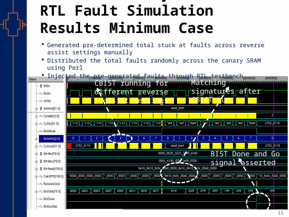
Results: Pre-Synthesis RTL Fault Simulation Results Minimum Case Generated pre-determined total stuck at faults across reverse assist
settings manually Distributed the total faults randomly across the canary SRAM using Perl Injected the pre-generated faults through RTL testbench
11
Matching signatures after CBIST run
BIST Done and Go signal asserted
CBIST running for different reverse assist settings

Rob
ust
Low
Power
VLSI 12
Results: Post-Synthesis RTL Fault Simulation Results Pass Case Synthesized using
IBM 130nm at SS_1.08V_-55C corner with 36ns (27.77MHz) Clock period
Able to detect BFR scenarios Nominal Minimum Maximum
Minimum BFR Case Output:Calc BFR Signature is: 6e1684108c0c80a000006e1684108c0c80a00000Read BFR Signature is: 6e1684108c0c80a000006e1684108c0c80a00000BIST Go No Go Status is: 1BIST Status Register Value is: ffff
0 1 2 3 4 5 6 7 80
100200300400500600
Max, Min, Nominal Write Bit Failure Rate vs. Reverse Assist Settings
Typical BFRMax BFRMin BFR
Reverse assist settingsN
umbe
r of w
rite
failu
res

Rob
ust
Low
Power
VLSI 13
0 1 2 3 4 5 6 7 80
100200300400500600
Faulty Write Bit Failure Rate vs. Reverse Assist Settings
Typical BFRMax BFRMin BFRFaulty BFR Case 1Faulty BFR Case 2Faulty BFR Case 3
Reverse assist settings
Num
ber o
f wri
te fa
ilure
s
Results: Post-Synthesis RTL Fault Simulation Results Fail Case
Able to detect BFR scenarios Overshoot Undershoot Non-monotonic
Signature comparison shows error in BIST Status register
Faulty BFR Case 3:Calc BFR Signature is: 7a990489541e00e05c007a990489541e00e05c00Read BFR Signature is: 7a990489541e00e05c007a990489541e00e05c00BIST Go No Go Status is: 0BIST Status Register Value is: d9d91101 1001 1101 1001

Rob
ust
Low
Power
VLSI 14
Results: Scan Insertion Used Synopsys’s DFT Compiler
Full scan chain
Estimated test coverage was 99.6%, however had issues in scan insertion and design rule check (DRC) errors were there that can cause fault simulation issue
Source: Dilip Vasudevan’s PhD thesis and a PPT from Kate, Yu-Jen Huang for DFT
Rob
ust
Low
Power
VLSI 15
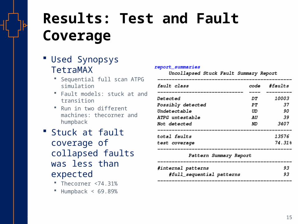
Results: Test and Fault Coverage Used Synopsys
TetraMAX Sequential full scan ATPG
simulation Fault models: stuck at and
transition Run in two different
machines: thecorner and humpback
Stuck at fault coverage of collapsed faults was less than expected Thecorner <74.31% Humpback < 69.89%

Rob
ust
Low
Power
VLSI 16
Results: Test and Fault Coverage Transition fault
coverage of collapsed faults was less than expected Thecorner < 64.74% Humpback < 64.56% Possible issue is DRC error
which occurred during the scan insertion
Did not got time to dig into it for a fix

Rob
ust
Low
Power
VLSI 17
Timeline
Deliverables Expected Date
Projected Date
Actual Date Status Issues
Architecture and Algorithm Design for
CBIST
2/16/2015 2/16/2015 Done none
Verilog entry of scan chain to BFR data table interface and simulation results
2/26/2015 2/26/2015 Done Having Verilog compilation
issues initially, but resolved
later.
Verilog entry of CBIST FSM and simulation
results
3/4/2015 03/4/2015 Done NA
Verilog entry of CBIST bitwise XOR, bit adder and error accumulator FSM and simulation
results
3/11/2015 03/9/2015 Done NA
Canary SRAM to CBIST interface and
full RTL integration for canary BIST in Verilog and simulation results
3/18/2015 3/25/2015 04/14/2015 Done Delayed due to time crunch. Will catch up
soon and complete.
Synthesis of Full CBIST using DC in
IBM 130nm
3/25/2015 3/27/2015 04/14/2015 Done Schedule changed. Will do that on 25th March week

Rob
ust
Low
Power
VLSI 18
Timeline ContinuedDeliverables Expected
DateProjected
DateActual Date Status Issues
Post synthesis verification of the
CBIST
3/30/2015 04/14/2015 Done Time issues
SPICE / DVE Simulation results of
CBIST pass/fail testing and test
access time
4/01/2015 04/14/2015 Done Time issues
Modeling the canary SRAM for stuck at
and canary BIST for delay faults
4/07/2015 04/14/2015 Done Time issues
Canary BIST Fault coverage results using TetraMAX
4/14/2015 04/14/2015 Done Time issues
Final Project Report 4/28/2015 Ongoing
Rob
ust
Low
Power
VLSI 19
Conclusions
The CBIST design shows promises to solves the issue of canary testing to see if canary with reverse assist can be used to track SRAM write VMIN.
We here only focused on canary write failure trend checking, but this hardware can be extended to readability testing also
Speed of the CBIST is not so good as the functionality is heavy and technology is 130nm
Scan insertion was a bit troublesome and had DFT DRC issues
Overall timeline was met successfully and the project was successful

Rob
ust
Low
Power
VLSI 20
References [1] J. Wang and B. Calhoun, “Canary replica feedback for near-DRV
standby vdd scaling in a 90 nm SRAM,” in Proc. Custom IntegratedCircuit Conf. (CICC ’07), Sep. 2007, pp. 29–32.
[2] Banerjee, A.; Sinangil, M.E.; Poulton, J.; Gray, C.T.; Calhoun, B.H., "A reverse write assist circuit for SRAM dynamic write VMIN tracking using canary SRAMs," Quality Electronic Design (ISQED), 2014 15th International Symposium on , vol., no., pp.1,8, 3-5 March 2014
[3] B. Zimmer, S. O. Toh, H. Vo, Y. Lee, O. Thomas, K. Asanovic, andB. Nikolic, “SRAM assist techniques for operation in a wide voltage rangein 28 nm CMOS,” IEEE Trans. Circuits Syst. II, vol. 59, no. 12, pp. 853–857, Dec. 2012.
[4] Fradi, A.; Nicolaidis, M.; Anghel, L., "Memory BIST with address programmability," On-Line Testing Symposium (IOLTS), 2011 IEEE 17th International , vol., no., pp.79,85, 13-15 July 2011
[5] Zarrineh, K.; Upadhyaya, S.J., "Programmable memory BIST and a new synthesis framework," Fault-Tolerant Computing, 1999. Digest of Papers. Twenty-Ninth Annual International Symposium on , vol., no., pp.352,355, 15-18 June 1999
[6] Kokrady, A.; Ravikumar, C.P.; Chandrachoodan, N., "Layout-Aware and Programmable Memory BIST Synthesis for Nanoscale System-on-Chip Designs," Asian Test Symposium, 2008. ATS '08. 17th , vol., no., pp.351,356, 24-27 Nov. 2008
[7] Ching-Hong Tsai; Cheng-Wen Wu, "Processor-programmable memory BIST for bus-connected embedded memories," Design Automation Conference, 2001. Proceedings of the ASP-DAC 2001. Asia and South Pacific , vol., no., pp.325,330, 2001


