© September 18, 2012 Dr. Lynn Fuller
Rochester Institute of Technology
Microelectronic Engineering
MEMs Lithography
Page 1
ROCHESTER INSTITUTE OF TEHNOLOGYMICROELECTRONIC ENGINEERING
9-18-2012 mem_lith.ppt
Microelectromechanical Systems (MEMs)Unit Processes for MEMs
Lithography
Dr. Lynn FullerWebpage: http://people.rit.edu/lffeee
Microelectronic EngineeringRochester Institute of Technology
82 Lomb Memorial DriveRochester, NY 14623-5604
Tel (585) 475-2035Fax (585) 475-5041
Email: [email protected] webpage: http://www.microe.rit.edu
© September 18, 2012 Dr. Lynn Fuller
Rochester Institute of Technology
Microelectronic Engineering
MEMs Lithography
Page 2
OUTLINE
PhotolithographyResist ProcessingLIGAThick ResistsSU-8Maskmaking for MEMsReversal ProcessingLift-OffTri-Layer ProcessesImaging PolyimidesReferencesHomework
© September 18, 2012 Dr. Lynn Fuller
Rochester Institute of Technology
Microelectronic Engineering
MEMs Lithography
Page 3
RAYLEIGH CRITERIA
DOF = λ λ λ λ / (2(NA)2)Lmin = 0.61 λ λ λ λ / NA
g-line i-line KrF ArF ArF
λλλλ 436 nm 365nm 248nm 193nm 193nm
NA 0.28 0.52 0.52 0.52 0.65
Lmin 0.95µm 0.50µm 0.30µm 0.23µm 0.18µm
DOF 2.78µm 0.8µm 0.46µm 0.36µm 0.23µm
© September 18, 2012 Dr. Lynn Fuller
Rochester Institute of Technology
Microelectronic Engineering
MEMs Lithography
Page 4
300 400 500 600 700
1.0i-line, 365 nm
g-line, 436 nm
0.5
0.0
Wavelength (nm)
h f
e
Resist Absorption
EMISSION SPECTRA OF THE Hg VAPOR BULB
© September 18, 2012 Dr. Lynn Fuller
Rochester Institute of Technology
Microelectronic Engineering
MEMs Lithography
Page 5
PHOTOLITHOGRAPHY
PhotomaskPhotoresistFilm to be PatterndSubstrate
Light
Negative Resist Positive Resist
Rendered Insoluble Rendered Soluble
After Development
After Etch and Strip
© September 18, 2012 Dr. Lynn Fuller
Rochester Institute of Technology
Microelectronic Engineering
MEMs Lithography
Page 6
PHOTORESIST PROCESSING
Substrate Cleaning
Priming
Spin Coating
Soft-Bake
Exposure
Post Exposure Bake
Develop
Rinse
Hard-Bake
Etching
Striping
© September 18, 2012 Dr. Lynn Fuller
Rochester Institute of Technology
Microelectronic Engineering
MEMs Lithography
Page 7
SUBSTRATE CLEAN AND PRIME
Cleaning is done with a high pressure (2000 psi) water scrub
A dehydration bake is typically done on a hot plate at 250 °Cfor 1 min. (Wafers are clean and dry just after removingfrom oxide growth furnace)
HMDS (hexa-methyl-di-silizane), TCPS, BSA - Adhesion promoter or primer: Are commonly applied as a liquidor vapor. HMDS attaches to remaining OH molecules releasing ammonia gas and creating an organic-like surface improving adhesion
Too much HMDS is detrimental to sensitivity and adhesion.
© September 18, 2012 Dr. Lynn Fuller
Rochester Institute of Technology
Microelectronic Engineering
MEMs Lithography
Page 8
RESIST SELECTION
S 1400 Pos g 50 0.6 1.8 0.1-2.8 120 1000 EGMEA
S 1800 Pos g 100 0.6 1.8 0.1-2.8 120 1000 PMA
EL 2026 Pos g, i 100 0.5 4.2 0.1-40 EL
OCG 825 Pos g,i 160 0.6 3 0.8-3 140 500 EEP
OMR-83 Neg i 30 2.5 175 Xylene
SAL 601 Neg ebeam 1uC/cm2 0.1 4 0.2-1.5 120 1000 EEA
Type
wavele
ngth
λλ λλ
(nm
)
Sensi
tivit
y (f
or
1 µ
m)
Reso
luti
on
(µm
)
Contr
ast
Thic
kness
(µ
m)
@ 4
000 r
pm
Soft
enin
g T
em
pera
ture
Boro
n a
nd I
ron (
ppm
)
Solv
ent
Type
© September 18, 2012 Dr. Lynn Fuller
Rochester Institute of Technology
Microelectronic Engineering
MEMs Lithography
Page 9
RESIST THICKNESS VS SPIN SPEED
70006000400030002000 5000
Spin Speed (rpm)
30 %, (20.30 cp)
26 %, (11.59 cp)
28 %, (15.23 cp)Th
ick
nes
s (µ
m)
0.7
1.1
1.3
32 %, (27.48 cp)
1.5
Most spin coating is performed at spin speeds from 3000 to 7000 RPM for 20 to 60 seconds, producing coating uniformities to +/- 100 Å
Example Only
© September 18, 2012 Dr. Lynn Fuller
Rochester Institute of Technology
Microelectronic Engineering
MEMs Lithography
Page 10
SOFT BAKE
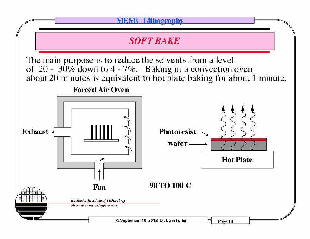
The main purpose is to reduce the solvents from a levelof 20 - 30% down to 4 - 7%. Baking in a convection ovenabout 20 minutes is equivalent to hot plate baking for about 1 minute.
Hot Plate
Exhaust Photoresist
wafer
Forced Air Oven
Fan 90 TO 100 C
© September 18, 2012 Dr. Lynn Fuller
Rochester Institute of Technology
Microelectronic Engineering
MEMs Lithography
Page 11
AUTOMATED COAT AND DEVELOP TRACK
© September 18, 2012 Dr. Lynn Fuller
Rochester Institute of Technology
Microelectronic Engineering
MEMs Lithography
Page 12
COAT AND DEVELOP TRACK
DEVELOPDI Wet
CD-26 Developer45sec. Puddle,30sec. Rinse,
40sec., 4000rpm Spin Dry
SPIN COAT
Shipley812 Resist
4500rpm, 60 sec.
SOFT BAKE
115 °C60 sec.
HARD BAKE
125 °C, 60 sec.
RECIPE 1 for all Tracks
DEHYDRATE BAKE/HMDS PRIMING
HMDS VaporPrime
140 °C, 60 sec.
© September 18, 2012 Dr. Lynn Fuller
Rochester Institute of Technology
Microelectronic Engineering
MEMs Lithography
Page 13
THICKNESS AFTER DEVELOP LOG DOSE
Resist Gamma, γγγγSlope
Norm
alized t
hic
kness
aft
er
Develo
p
Log Dose (mj/cm2)
Dc
0
0.5
1.0
D(0)
Dc is the dose to clearD(0) is the max dose for
unexposed areas
The higher the slope or contrast, gamma, then the smaller the difference needs to be between exposure in areas to be cleared and areas to leave resist. That is the required airal image modulation is smaller.
© September 18, 2012 Dr. Lynn Fuller
Rochester Institute of Technology
Microelectronic Engineering
MEMs Lithography
Page 14
EXPOSURE
E = I t
where E is exposure dose in mj/cm2, I is irradianc in mw/cm2, t is exposure time in seconds
Humidity should be 45% the exposed PAC requires water to convert to carboxilic acid
Post exposure bake increases speed of resist
Post exposure bake reduces standing wave effects
Post exposure bake is require for chemically amplified and image reversal resists (100 to 115 C for 1 min.)
© September 18, 2012 Dr. Lynn Fuller
Rochester Institute of Technology
Microelectronic Engineering
MEMs Lithography
Page 15
GCA 6700 STEPPER
g-Line Stepper λ = 436 nmNA = 0.28σ = 0.6Resolution0.6 λ / NA = ~1µm20 x 20 mm Field SizeDepth of Focus= k2 λ/(NA)2 = 3 µm
Stepper Job: [10,1]MEMS2000Pass: 1 (poly1), 2 (via), 3 (anchor), 4 (poly2)
© September 18, 2012 Dr. Lynn Fuller
Rochester Institute of Technology
Microelectronic Engineering
MEMs Lithography
Page 16
ASML 5500/200
NA = 0.48 to 0.60 variableσ= 0.35 to 0.85 variable
With Variable Kohler, orVariable Annular illuminationResolution = K1 λ/NA
= ~ 0.35µm for NA=0.6, σ =0.85
Depth of Focus = k2 λ/(NA)2
= > 1.0 µm for NA = 0.6i-Line Stepper λ = 365 nm
22 x 27 mm Field Size
© September 18, 2012 Dr. Lynn Fuller
Rochester Institute of Technology
Microelectronic Engineering
MEMs Lithography
Page 17
EXPOSURE TOOLS
SEE www.suss.comcontact printers
with back side alignment
Karl Suss Aligner at RIT
© September 18, 2012 Dr. Lynn Fuller
Rochester Institute of Technology
Microelectronic Engineering
MEMs Lithography
Page 18
DEVELOP
Develop is done in an alkali solution such as NaOH or KOH (Metal Containing Developers) Trace quantities of these metals can cause transistor threshold voltage shifts. These developers give higher contrast and are less expensive than metal ion free.
Metal Ion Free Developers are available.
Developer Concentration and Temperature of Developer are the most important parameters to control.
© September 18, 2012 Dr. Lynn Fuller
Rochester Institute of Technology
Microelectronic Engineering
MEMs Lithography
Page 19
HARD BAKE
Hard Bake is done at or slightly above the glass transition temperature. The resist is crosslinked (and is toughened prior to plasma etch). The resist flows some as shown below. Pinholes are filled. Improves adhesion also. No flow should occur at the substrate. Photo stabilization involves applying UV radiation and heat at 110C for dose of 1000 mj/cm2 then ramping up the temperature to 150-200 C to complete the photostabilization process.
After Develop After Hard Bake
125 to 140 C for 1 min.
© September 18, 2012 Dr. Lynn Fuller
Rochester Institute of Technology
Microelectronic Engineering
MEMs Lithography
Page 20
ETCH
Wet etchesAcids – can be usedBases – can not be used with positive photoresist
Plasma etchesFlourine based etches – etches photoresist at ~0.2 µm/min
Isotropic etches availableAnisotropic etches available
© September 18, 2012 Dr. Lynn Fuller
Rochester Institute of Technology
Microelectronic Engineering
MEMs Lithography
Page 21
RESIST STRIP
Asher
O2 + Energy = 2 O
O is reactive and will combinewith plastics, wood, carbon, photoresist, etc.
© September 18, 2012 Dr. Lynn Fuller
Rochester Institute of Technology
Microelectronic Engineering
MEMs Lithography
Page 22
NOVEL RESIST PROCESSES
LIGA ProcessSU-8 Thick ResistsReversal ProcessingLift-off ProcessesTri-layer ProcessesElectrodeposited ResistNano-imprint Technology
Maskmaking for MEMs
© September 18, 2012 Dr. Lynn Fuller
Rochester Institute of Technology
Microelectronic Engineering
MEMs Lithography
Page 23
LIGA
LIGA method is based on a combination of deep-etch x-ray lithography, electroforming and molding. (in German: Lithographie, Galvanoformung, Abformung)
X-ray resist image
Electroplatednickel mold
© September 18, 2012 Dr. Lynn Fuller
Rochester Institute of Technology
Microelectronic Engineering
MEMs Lithography
Page 24
LIGA
X-ray lithography has depth of focusthat is measured in cm. This structureis ~400 µm in height
© September 18, 2012 Dr. Lynn Fuller
Rochester Institute of Technology
Microelectronic Engineering
MEMs Lithography
Page 25
LIGA
Honeycomb structure in PMMA.Openings of 80 µm, wall thicknessof 7 µm
© September 18, 2012 Dr. Lynn Fuller
Rochester Institute of Technology
Microelectronic Engineering
MEMs Lithography
Page 26
SU-8 RESIST
Microlithography Chemical Company
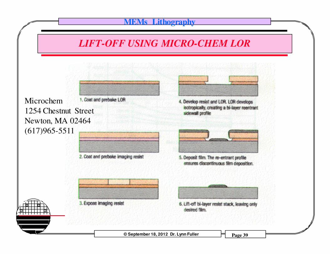
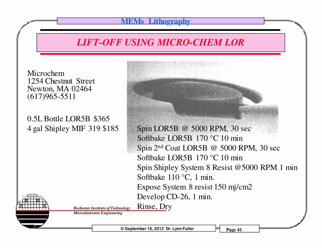
MicroChem Corp.,1254 Chestnut Street, Newton, MA 02464. Tel: (617)965-5511Fax: (617) 965-5818, makes SU-8, LOR and other resist systems
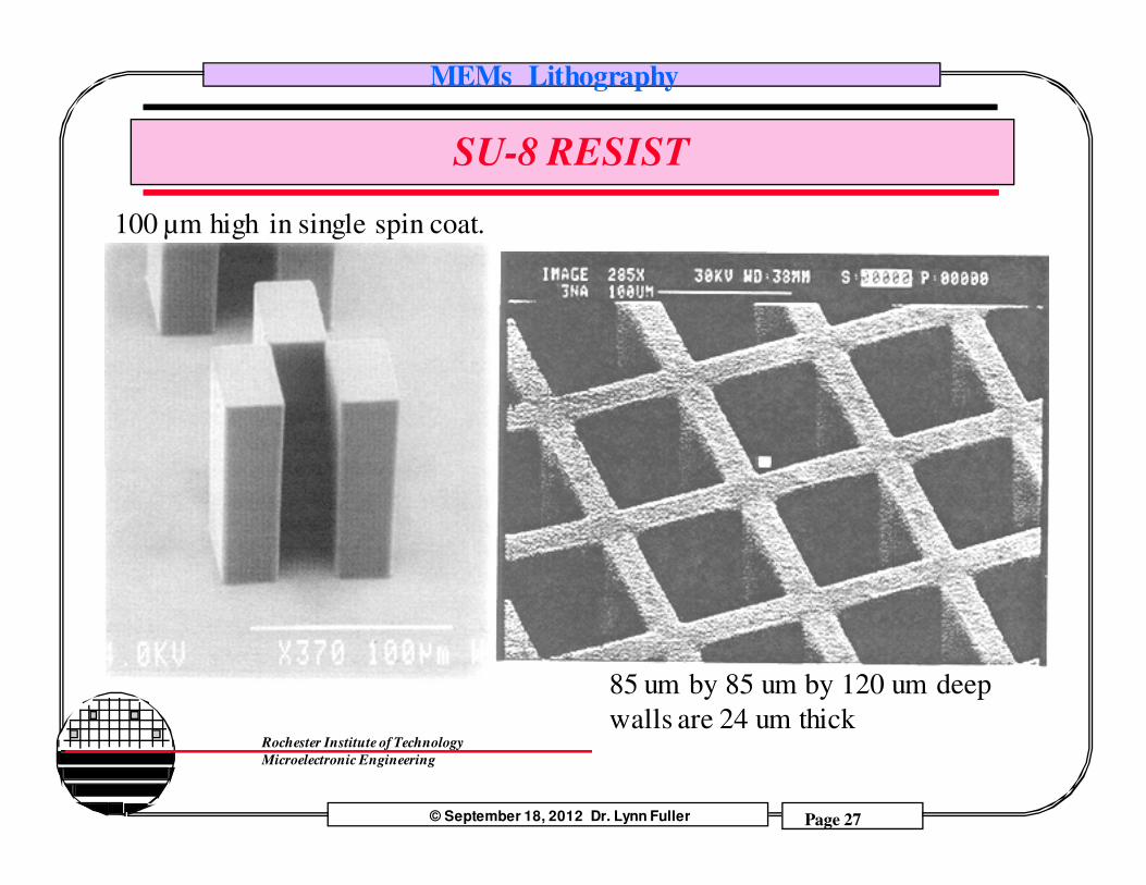
SU-8 is an Epoxy Photoresist coatings 50-500 um thickness
(does not strip in acetone, oxygen plasma strip is possible buttakes 50 to 500 times longer than a 1 um coating so RIE oxygenplasma, high pressure water and other techniques are used.)
Electroplate nickel on 500 A chrome, 3000 A copper base layer
When using a mold use polydimethylsiloxane (PDMS) mold release
Jenoptik makes HEX 03 hot embossing system or do by homemade150 C, vacuum forming, 45 min
MORE
© September 18, 2012 Dr. Lynn Fuller
Rochester Institute of Technology
Microelectronic Engineering
MEMs Lithography
Page 27
SU-8 RESIST
85 um by 85 um by 120 um deep walls are 24 um thick
100 µm high in single spin coat.
© September 18, 2012 Dr. Lynn Fuller
Rochester Institute of Technology
Microelectronic Engineering
MEMs Lithography
Page 28
SU-8 RESIST at RIT
© September 18, 2012 Dr. Lynn Fuller
Rochester Institute of Technology
Microelectronic Engineering
MEMs Lithography
Page 29
SU-8 RESIST PROCESSING at RIT
Dehydration Bake on Hotplate at 250 C for 5 minCool for 3 minDispense SU-8 10 by pouring out of the bottle. (we have SU-8-10, SU-8
2002, 2015 and 2050 materialSpread @ 500 RPM for 5 secondsSpin @ 3000 rpm for 30 sec.Leave on the wafer on the spinner to self planarize for 5 min.(no vacuum)Pre Bake at 55 C for 5 min in a convection oven or Solitec 0.5 cm above
90 °C hot plate. Soft Bake at 90 C for 6 min on a hotplateCool for 5 minExpose using Karl Suss contact aligner
E = 175 mJ/cm2 (for ~10 um thick resist)PEB Bake 90 C on hotplate for 15 min in a convection oven or Solitec 0.5
cm above 90 °C hot plate for 5 min then 15 min on hot plateCool for 15 min
Develop in RER 600 (100% PGMEA) Developer, for 3 min with constant vigorous agitation
Rinse with IPASpin or Blow Dry
© September 18, 2012 Dr. Lynn Fuller
Rochester Institute of Technology
Microelectronic Engineering
MEMs Lithography
Page 30
Dynachem EL2026 Thick Film Positive Photoresist gives thickness between 2 and 100 µm. Bake in convection over at 90 C for 30 min. Best focus is 240 not the normal 250 for a 10 um coating. Exposure dose is 4500 mj/cm2. Develop is 0.35 Normal KOH developer for 10 min. Hardbake 100 C for 30 min in convection oven.
AZ 4000 Series Photoresists, Hoechst, 3070 Highway 22 West, Somerville, NJ 08876, (201) 231-3889, for Thick Film Applications: AZ4330 is 35.5 % solids for 2.9 µm @ 5000 rpm, AZ4400 for 3.5 µm @ 5000 rpm, AZ4620 for 5.6 µm @ 5000 rpm and 7.1 µm at 3000 rpm. AZ P4620 gives 30 µm thickness, AZ PLP 100 gives 50 µm thickness, Develop with AZ400K diluted 1:3. AZ4901 is formulated for spray and can coat up to 50 µm thick.
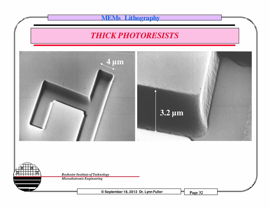
THICK PHOTORESISTS
Multiple coatings give thicker resist layers. In between each coating bake at 90 C for 30 seconds on the hot plate. Use low spin speeds even as low as 1240 rpm.
Exposure needs to be increased start with 100 mj/cm2 for each 1µm thickness of resist.
AZ P4620 (10 µm)
© September 18, 2012 Dr. Lynn Fuller
Rochester Institute of Technology
Microelectronic Engineering
MEMs Lithography
Page 31
We tried coating Shipley system 8 resist at low spin speed to see how thick of a coating we could get. We got 1.7um @ 2000rpm, 1.2um @ 3000rpm and 1.0um @ 4000rpm. Exposure on the stepper at 200 mj/cm2 (0.8 seconds in integrate mode) worked with hand develop of 1 min. using Shipley 321 developer.
We also tried OCG ASPR-528 at RIT, the resist coated at 4500 rpm gave a thickness of 2.9 µm after a soft bake of 115 C for 1 min, and 1 sec exposure on the stepper for 250 mj/cm2 in integrate mode and develop in straight Shipley 321 developer for 1 min 30 seconds gives good images.
ExposureSpeed Thickness Dose5000 rpm 25,000 Å 400mj/cm24500 27,3004000 31,550 5003500 33,1003000 35,500 6002500 37,6002000 41,000 700
THICK PHOTORESISTS
© September 18, 2012 Dr. Lynn Fuller
Rochester Institute of Technology
Microelectronic Engineering
MEMs Lithography
Page 32
THICK PHOTORESISTS
3.2 µm
4 µm
© September 18, 2012 Dr. Lynn Fuller
Rochester Institute of Technology
Microelectronic Engineering
MEMs Lithography
Page 33
THICK RESISTS
Molds for electroplated
MEM structures
20 µm
THICK RESISTS
© September 18, 2012 Dr. Lynn Fuller
Rochester Institute of Technology
Microelectronic Engineering
MEMs Lithography
Page 34
PHOTOSENSITIVE FILMS
http://www.rayzist.com/
Also ImageOn fromRIT Bookstore 12”x10’x0.002” thickfor $18
© September 18, 2012 Dr. Lynn Fuller
Rochester Institute of Technology
Microelectronic Engineering
MEMs Lithography
Page 35
NEGATIVE PHOTORESIST FILM PROCESSING
ImageOn Processing –negative working resist, 50µm Thick
Wet SubstrateRemove mylar film from the non-shiny side of the resistPlace resist on the wet substrateRemove water from center to edge, remove top mylar film
Repeat to get 100, 150, 200 µm total thicknessHeat cure the resist to improve adhesion???Expose: Dose = ~50 mj/cm2,
Iradiance = 3.5mW/cm2 x 15 sec30 for 100µm, 45 for 150µm, etc.
Remove top mylar filmDevelop for 60sec in CD26 (develop 15 sec, spray DI water,
repeat every 15 sec until clearRinse with water and dryHard bake
© September 18, 2012 Dr. Lynn Fuller
Rochester Institute of Technology
Microelectronic Engineering
MEMs Lithography
Page 36
150µm DEEP CHANNELS
© September 18, 2012 Dr. Lynn Fuller
Rochester Institute of Technology
Microelectronic Engineering
MEMs Lithography
Page 37
1 Dehydration Bake at 200 °C, 3 minutes.2 Spin coat AZ-5214-E photoresist - 4000rpm / 45sec3 Pre-bake on hotplate - 100°C / 45sec4 Expose 80 mj/cm2, (about 10 seconds on Kasper contact aligner) or (800 mj/cm2 on the stepper, because stepper is G-line and Kasper is wide band exposure)5 Post exposure bake, image reversal (PEB) on hotplate - 115°C / 90sec6 Flood expose on Kasper aligner - 30sec 7 Develop 20 sec. in Shipley 351 + H2O (1:4 ratio) in petri dish
- mix 100ml developer with 400ml H2O -rinse immediately after develop
8 Blow Dry. 9 Postbake on hotplate - 100°C / 1min
Coat
Photoresist
Substrate
Expose
Normal Process
No Extra Processing
Reversal Process
Post Exposure Reversal BakeFlood Expose
After Development
After Development
REVERSAL PROCESSING
MORE
© September 18, 2012 Dr. Lynn Fuller
Rochester Institute of Technology
Microelectronic Engineering
MEMs Lithography
Page 38
LIFT-OFF
1. Create a reverse slope or undercut resist edge profile
2. Deposit film by evaporation
3. Chemically strip photoresist and lift off film, leaving film in desired pattern
Substrate
Photoresist Film
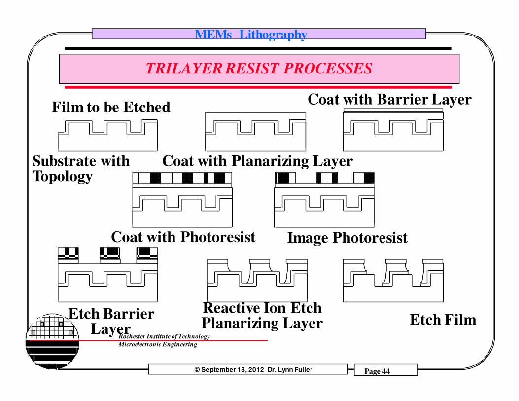
These undercut resist profiles are created by several techniques:1. Chlorobenzene induced lip in single layer photoresist2. Bilayer resists where top layer developes slower3. Special undercoatings that develop faster than resist in developer4. Trilayer methods5. Image reversal resists
MORE
© September 18, 2012 Dr. Lynn Fuller
Rochester Institute of Technology
Microelectronic Engineering
MEMs Lithography
Page 39
LIFT-OFF USING MICRO-CHEM LOR
Microchem1254 Chestnut StreetNewton, MA 02464(617)965-5511
© September 18, 2012 Dr. Lynn Fuller
Rochester Institute of Technology
Microelectronic Engineering
MEMs Lithography
Page 40
LIFT-OFF USING MICRO-CHEM LOR
© September 18, 2012 Dr. Lynn Fuller
Rochester Institute of Technology
Microelectronic Engineering
MEMs Lithography
Page 41
LIFT-OFF USING MICRO-CHEM LOR
0.5L Bottle LOR5B $3654 gal Shipley MIF 319 $185 Spin LOR5B @ 5000 RPM, 30 sec
Softbake LOR5B 170 °C 10 minSpin 2nd Coat LOR5B @ 5000 RPM, 30 secSoftbake LOR5B 170 °C 10 minSpin Shipley System 8 Resist @5000 RPM 1 minSoftbake 110 °C, 1 min.Expose System 8 resist 150 mj/cm2Develop CD-26, 1 min.Rinse, Dry
Microchem1254 Chestnut StreetNewton, MA 02464(617)965-5511
© September 18, 2012 Dr. Lynn Fuller
Rochester Institute of Technology
Microelectronic Engineering
MEMs Lithography
Page 42
AZ nLOF 2000 Photoresist
RIT process, spin at 3000rpm 30 sec, bake 95°C for 90 s, Expose 120 mj/cm2 on Canon, Develop.rcp on SSI track
© September 18, 2012 Dr. Lynn Fuller
Rochester Institute of Technology
Microelectronic Engineering
MEMs Lithography
Page 43
PHOTOPATTERNABLE SILICONE MATERIALS
www.DowCorning.com
© September 18, 2012 Dr. Lynn Fuller
Rochester Institute of Technology
Microelectronic Engineering
MEMs Lithography
Page 44
TRILAYER RESIST PROCESSES
Substrate withTopology
Film to be Etched
Coat with Planarizing Layer
Coat with Barrier Layer
Coat with Photoresist Image Photoresist
Etch BarrierLayer
Reactive Ion EtchPlanarizing Layer Etch Film
© September 18, 2012 Dr. Lynn Fuller
Rochester Institute of Technology
Microelectronic Engineering
MEMs Lithography
Page 45
Polyimide has a melting point of 450 C, can be spin coated and imaged with lithographic processes making it useful for many applications.Using DuPont Corporations PI-2555 we can get film thickness between 2.5 µm @ 5000 rpm and 5.0 µm @ 1500 rpm. It is cured by placing on 120 °C hot plate for 30 min. and then on a 350 °C hot plate for 30 min. Multilayer coatings can give thickness greater than 10 µm. (a 500 gm bottle costs ~$250) Du Pont Co., Electronic Materials Division, Barley Mill Plaza, Reynolds Mill Building, Wilmington, DE 19898 (800)441-7543OCG Microelectronic Materials, Belgium, makes a polyimide “Proimide 114A” which we have used.These film are easily imaged using an aluminum barrier layer and conventional photoresist (such as Shipley System-8) followed by Oxygen Reactive Ion Etch.
POLYIMIDE
© September 18, 2012 Dr. Lynn Fuller
Rochester Institute of Technology
Microelectronic Engineering
MEMs Lithography
Page 46
ETCHING OF POLYIMIDE IN GEC CELL
Use GEC Cell, Time=75 min, Pressure=300 mTorr, Power = 60 watts, Flow = 50 sccm, Gas=Oxygen, Give an Etch Rate of 1300 Å/min (7.8 um/hr)
Higher etch rates can be obtained with addition of a small amount of CF4. Note: CF4 also etches silicon, silicon dioxide, and silicon nitride.
GEC cell at 300 mTorr, 45 sccm O2, 5 sccm CF4, 60 watts, 30 min for 10 µm of Polyimide, (~20µm/hr)
© September 18, 2012 Dr. Lynn Fuller
Rochester Institute of Technology
Microelectronic Engineering
MEMs Lithography
Page 47
CONFORMAL RESIST COATINGS
http://www.elvisions.comElectronic Visions Inc. (602 437-9492
Uniform conformal coatings on sidewallsand in cavities.
© September 18, 2012 Dr. Lynn Fuller
Rochester Institute of Technology
Microelectronic Engineering
MEMs Lithography
Page 48
ELECTRODEPOSIED RESIST COATINGS
© September 18, 2012 Dr. Lynn Fuller
Rochester Institute of Technology
Microelectronic Engineering
MEMs Lithography
Page 49
NANOIMPRINT LITHOGRAPHY
1. Substrate is coated with photoresist.2. Substrate is heated above the glass transistion temperature.3. A hard mold is pressed against the substrate deforming the resist.4. The substrate and resist is cooled5. The hard mold is removed6. The resist is plasma etched (RIE) in Oxygen to remove residual resist.7. Substrate is etched.
© September 18, 2012 Dr. Lynn Fuller
Rochester Institute of Technology
Microelectronic Engineering
MEMs Lithography
Page 50
NANOIMPRINT
© September 18, 2012 Dr. Lynn Fuller
Rochester Institute of Technology
Microelectronic Engineering
MEMs Lithography
Page 51
PLATING
Using a patterned photoresist layer. Wafers can be electroplated in those areas creating structures without etching.
1 mm Electroplatednickel
PhotoresistPatternPlated Copper Gears
© September 18, 2012 Dr. Lynn Fuller
Rochester Institute of Technology
Microelectronic Engineering
MEMs Lithography
Page 52
MASKMAKING FOR MEMS
Maskmaking is normal except for mask sets that include masks to image the backside of the wafer. In order to get alignment, the masks for the back side need to be mirrored with respect to the front side masks.
Letter R on top of waferrequires a mask that is
wrong reading from chrome side
Letter R on bottom of wafer aligned with R on
top requires correct reading mask image from chrome side
© September 18, 2012 Dr. Lynn Fuller
Rochester Institute of Technology
Microelectronic Engineering
MEMs Lithography
Page 53
STEREO LITHOGRAPHY
10 µm 10 µm
Two infrared lasers causes plastic resin to polymerize. Professor Satoshi Kawata of Osaka University
© September 18, 2012 Dr. Lynn Fuller
Rochester Institute of Technology
Microelectronic Engineering
MEMs Lithography
Page 54
REFERENCES
1. Micromechanics and MEMs, Edited by William S. Trimmer, IEEE Press.
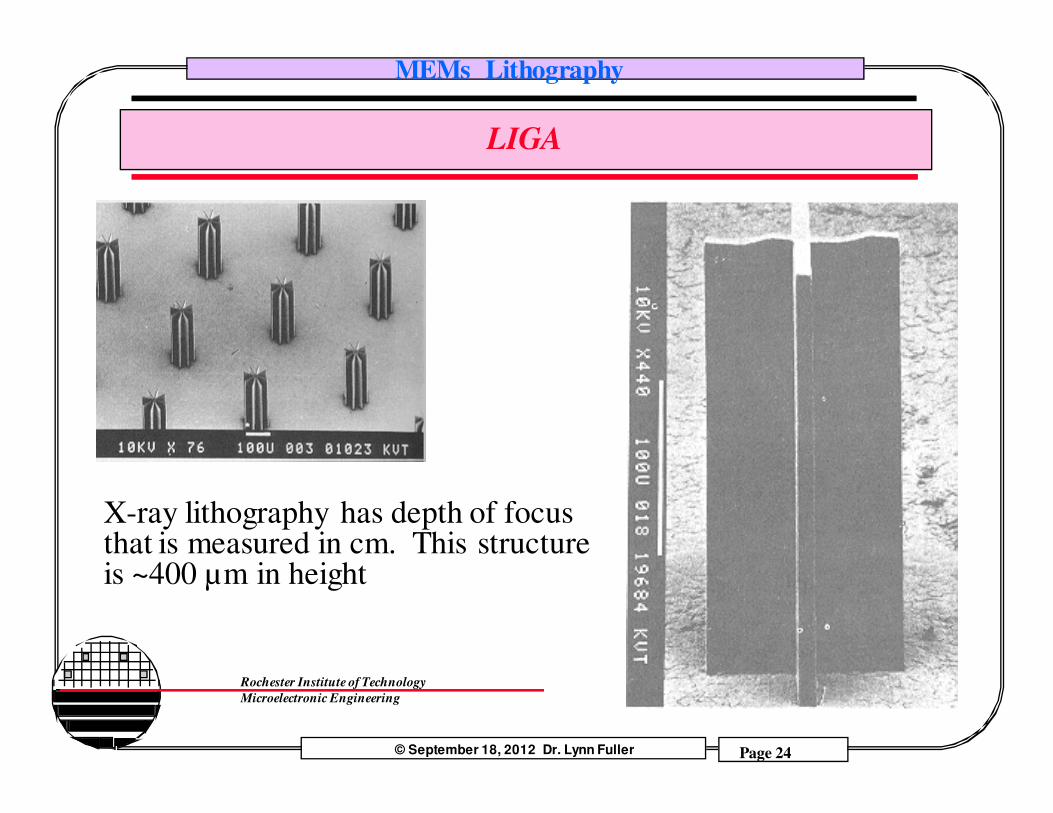
2. Fabrication of Microstructures Using the LIGA Process, W. Ehrfeld, et.al., Proceedings of IEEE Micro Robots and Teleoperators Workshop, November 1987.
3. “Image Reversal Resist for g-line Exposure: Chemistry and Lithographic Evaluation,” Gerhard Buhr, Helmut Lenz and Siegfried Scheler, R & D Informationstechnik-Division, Hoechst Aktiengesellschaft Werk Kalle, D-6200 Wiesbaden
4. “Single-Step Otical Lift-Off Process,” M. Hatzakis, B.J. Canavello, J.M. Shaw, IBM J. Res, Develop, Vol 24, No.4, July, 1980.
5. www.microchem.com
6. Dupont
© September 18, 2012 Dr. Lynn Fuller
Rochester Institute of Technology
Microelectronic Engineering
MEMs Lithography
Page 55
HOMEWORK – MSMS LITHOGRAPHY
1. What makes lithography for MEMs different than lithography for integrated circuits?
2. Compare the depth of focus for RIT’s g-line stepper with RIT’s i-line stepper.
3. What resist thickness is needed to plasma etch a 2µm thick silicon dioxide layer? (assume SiO2 etch rate = 350Å/min and Photoresistetch rate = 220Å/min.)
4. What is the purpose of the hard bake? When would you not do hard bake? Why?
5. Explain how lift-off works. What are the advantages of using lift-off?