Monday Dec. 14 Room A 7:00-8:00AM Breakfast Session: Crystal Engineering I Chair: Cristian V. Ciobanu 8:00-8:25AM A01: Laser-irradiation-induced crystallization of Si films: scientific opportunities and technological motivations James Im Columbia University, USA 8:25-8:50AM A02: Multi crystalline silicon solidification under controlled forced convection Kader Zaidat Institut Polytechnique de Grenoble – PHELMA, France 8:50-9:15AM A03: Thermodynamic Phase Behavior of Cocrystal Systems Gabriele Sadowski TU Dortmund, Germany 9:15-9:40AM A04: The effect of crystalline environment on molecular interactions in crystals : A further (unknown) variable in crystal engineering Enrique Espinosa University of Lorraine, France 9:40-10:05AM A05: Continuous crystallization of pharmaceuticals Richard Lakerveld The Hong Kong University of Science & Technology, Hong Kong 10:05-10:20AM Session Break Session: Epitaxial thin films and nanostructures I Chair: Bernd Rauschenbach 10:20 -10:45AM A06: Stability and Electrical ZnIn2O4 Thin Film with Cubic Spinel Structure as a Novel Transparent Conductive Oxide Naoki Wakiya Shizuoka University, Japan 10:45-11:10AM A07: Sub-monolayer InAs/GaAs depositions without and with Sb for fast, directly driven laser devices Holger Eisele Technische Universitä t Berlin, Germany 11:10-11:35AM A08: Real time observation of nanowire growth and selective growth of nanocrystals Tomas Sikola Brno University of Technology, Czech Republic 11:35-12:00PM A09: Novel Dilute Bismides for IR Optoelectronics Shumin Wang Chalmers University of Technology, Sweden 12:00-12:25PM A10: Magnetic domain wall manipulation in tailored (Ga,Mn)As nanostructures for spintronic applications Tadeusz Wosinski Polish Academy of Sciences, Poland 12:30-13:30PM Lunch Break
Transcript
Monday Dec. 14
Room A
7:00-8:00AM Breakfast
Session: Crystal Engineering I Chair: Cristian V. Ciobanu
8:00-8:25AM
A01: Laser-irradiation-induced
crystallization of Si films: scientific
opportunities and technological
motivations
James Im
Columbia University, USA
8:25-8:50AM
A02: Multi crystalline silicon
solidification under controlled forced
convection
Kader Zaidat
Institut Polytechnique de Grenoble –
PHELMA, France
8:50-9:15AM A03: Thermodynamic Phase Behavior of
Cocrystal Systems
Gabriele Sadowski
TU Dortmund, Germany
9:15-9:40AM
A04: The effect of crystalline
environment on molecular interactions in
crystals : A further (unknown) variable in
crystal engineering
Enrique Espinosa
University of Lorraine, France
9:40-10:05AM A05: Continuous crystallization of
pharmaceuticals
Richard Lakerveld
The Hong Kong University of Science &
Technology, Hong Kong
10:05-10:20AM Session Break
Session: Epitaxial thin films and nanostructures I Chair: Bernd Rauschenbach
10:20 -10:45AM
A06: Stability and Electrical ZnIn2O4
Thin Film with Cubic Spinel Structure as
a Novel Transparent Conductive Oxide
Naoki Wakiya
Shizuoka University, Japan
10:45-11:10AM
A07: Sub-monolayer InAs/GaAs
depositions without and with Sb for fast,
directly driven laser devices
Holger Eisele
Technische Universität Berlin, Germany
11:10-11:35AM
A08: Real time observation of nanowire
growth and selective growth of
nanocrystals
Tomas Sikola
Brno University of Technology, Czech
Republic
11:35-12:00PM A09: Novel Dilute Bismides for IR
Optoelectronics
Shumin Wang
Chalmers University of Technology,
Sweden
12:00-12:25PM
A10: Magnetic domain wall
manipulation in tailored (Ga,Mn)As
nanostructures for spintronic
applications
Tadeusz Wosinski
Polish Academy of Sciences, Poland
12:30-13:30PM Lunch Break
Monday Dec. 14
Room B
Session: Epitaxial thin films and nanostructures II Chair: Tadeusz Wosinski
13:30-13:55PM B01: Sheathed Nanowires Aligned by
Crystallographic Periodicity
Hiroshi M. Yamamoto
Institute for Molecular Science, Japan
13:55-14:20PM
B02: 3D Nanostructured Materials via
Atomic Layer Deposition: Fabrication &
Solar Energy Harvesting / Smart
Window Applications
Alfred Tok
Nanyang Technological University,
Singapore
14:20-14:45PM B03: SiGe Sputter Epitaxy and Its
Application to SiGe 2D Devices
Yoshiyuki Suda
Tokyo University of Agriculture and
Technology, Japan
14:45-15:00PM
B04: Development of MBE Air-Hole
Retained Growth Technique for
Fabrication of Photonic-Crystal Lasers
Masaya Nishimoto
Kyoto University, Japan
15:00-15:15PM
B05: Synthesis of High Performance
Co(Soft)/SmCo5(Hard) Nanocomposite
Magnets by Core/Shell Nanoparticles for
Exchange-coupled Nanocomposite
Inho Kim
Sogang University, Korea
15:15-15:25PM Session Break
Session: Epitaxial thin films and nanostructures III Chair: Yoshiyuki Suda
15:25-15:50PM
B06: Epitaxial GaN films prepared by
hyperthermal ion beam assisted
molecular beam epitaxy - an
electronmicroscopical study
Bernd Rauschenbach
IOM and University Leipzig, Germany
15:50-16:15PM
B07: Concurring kinetics of phase
transition and grain growth in
nanostructured alloy
Feng Liu
Northwestern Polytechnical University,
China
16:15-16:40PM
B08: Epitaxial Growth of Lead-free
Piezoelectric Thin films and
Superlattices
Danyang Wang
University of New South Wales, Australia
16:40-17:05PM B09: The unique physical properties of
nanostructured diamond
Changzhi Gu
Institute of Physics, CAS, China
17:30PM Dinner Social
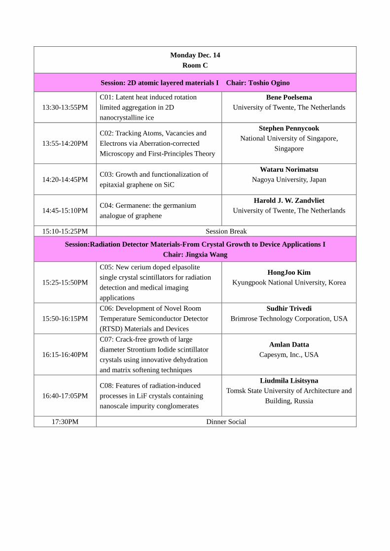
Monday Dec. 14
Room C
Session: 2D atomic layered materials I Chair: Toshio Ogino
13:30-13:55PM
C01: Latent heat induced rotation
limited aggregation in 2D
nanocrystalline ice
Bene Poelsema
University of Twente, The Netherlands
13:55-14:20PM
C02: Tracking Atoms, Vacancies and
Electrons via Aberration-corrected
Microscopy and First-Principles Theory
Stephen Pennycook
National University of Singapore,
Singapore
14:20-14:45PM C03: Growth and functionalization of
epitaxial graphene on SiC
Wataru Norimatsu
Nagoya University, Japan
14:45-15:10PM C04: Germanene: the germanium
analogue of graphene
Harold J. W. Zandvliet
University of Twente, The Netherlands
15:10-15:25PM Session Break
Session:Radiation Detector Materials-From Crystal Growth to Device Applications I
Chair: Jingxia Wang
15:25-15:50PM
C05: New cerium doped elpasolite
single crystal scintillators for radiation
detection and medical imaging
applications
HongJoo Kim
Kyungpook National University, Korea
15:50-16:15PM
C06: Development of Novel Room
Temperature Semiconductor Detector
(RTSD) Materials and Devices
Sudhir Trivedi
Brimrose Technology Corporation, USA
16:15-16:40PM
C07: Crack-free growth of large
diameter Strontium Iodide scintillator
crystals using innovative dehydration
and matrix softening techniques
Amlan Datta
Capesym, Inc., USA
16:40-17:05PM
C08: Features of radiation-induced
processes in LiF crystals containing
nanoscale impurity conglomerates
Liudmila Lisitsyna
Tomsk State University of Architecture and
Building, Russia
17:30PM Dinner Social
Monday Dec. 14
Room D
Session: Tunable materials Chair: Holger Eisele
13:30-13:55PM D01: Gold(I) Compounds with Tunable
Luminescent Properties
Andrea Deak
Hungarian Academy of Sciences, Hungary
13:55-14:20PM
D02: Controlled nucleation and growth
in glass and its impact on glass
bioactivity
Jonathan Massera
Tampere University of Technology, Finland
14:20-14:45PM D03: Thin films from topological
crystalline insulators
Marta Galicka
Polish Academy of Sciences, Poland
14:45-15:10PM D04: Glass-ferroic composite: the third
class of ferroic materials
Yuanchao Ji
Xi'an Jiaotong University, China
15:10-15:25PM Session Break
Session: General I Chair: Geun Woo Lee
15:25-15:50PM
D05: Importance of water in the control
of inorganic crystal growth by organic
molecules
Hiroki Nada
National Institute of Advanced Industrial
Science and Technology (AIST)
Japan
15:50-16:15PM
D06: Synthesis of Graphene / MxWO3
Composite with Excellent Electrical
Properties
Shu Yin
Tohoku University, Japan
16:15-16:40PM
D07: Convection diffusion models
accompanied with gas-phase epitaxy of
semiconducting layers
Pavel Boldyrevskii
Nizhny Novgorod Lobachevsky State
University, Russia
16:40-17:05PM D08: Fluoride crystals as potential
vacuum ultraviolet laser media
Nobuhiko Sarukura
Osaka University, Japan
17:30PM Dinner Social
Tuesday Dec. 15
Room B
7:00-8:00AM Breakfast
Session: Epitaxial thin films and nanostructures IV Chair: Elisabeth Blanquet
8:00-8:25AM
B10: Eliminating defects in
three-dimensional micro- and
nanocrystals on mismatched substrates
Hans Von Känel
ETH Zürich, Switzerland
8:25-8:50AM B11: Growth of atomically flat diamond
films
Norio Tokuda
Kanazawa University, Japan
8:50-9:15AM
B12: Hybrid Magnetic/Semiconductor
Materials : Growth, Structure and
Properties
Yongbing Xu
Nanjing University, China; The University
of York, UK
9:15-9:40AM B13: Heteroepitaxial growth of layered
pnictides and chalcogenides films
Hidenori Hiramatsu
Tokyo Institute of Technology, Japan
9:40-10:05AM B14: Epitaxial growth of gamma-phase
Ga2O3 semiconductor
Takayoshi Oshima
Tokyo Institute of Technology, Japan
10:05-10:20AM Session Break
Session: General II Chair: Pallavi Kushwaha
10:20 -10:45AM B15: Lattice Model Analysis Combined
with LEEM Observations
Noriko Akutsu
Osaka Electro-Communication University,
Japan
10:45-11:10AM
B16: Numerical Simulation of
Development of Sea Ice Microstructure
with Particle Method and Voronoi
Dynamics
Yoshiki Kawano
National Institute of Technology, Japan
11:10-11:35AM
B17: Structure-function correlations in
metal oxides – Insights from density
functional and many body theory
Eva Rauls
Universität Paderborn, Germany
11:35-12:00PM
B18: Bipartite bosonic modes and spin
memory effects in superconducting
Sr4V2O6Fe2As2 investigated with
variable temperature/field spin-polarized
STM
Jhinhwan Lee
KAIST, Korea
12:00-13:30PM Lunch Break
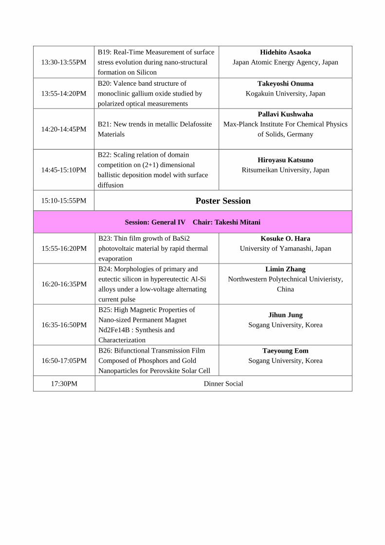
Session: Gereral III Chair: Yoshiki Kawano
13:30-13:55PM
B19: Real-Time Measurement of surface
stress evolution during nano-structural
formation on Silicon
Hidehito Asaoka
Japan Atomic Energy Agency, Japan
13:55-14:20PM
B20: Valence band structure of
monoclinic gallium oxide studied by
polarized optical measurements
Takeyoshi Onuma
Kogakuin University, Japan
14:20-14:45PM B21: New trends in metallic Delafossite
Materials
Pallavi Kushwaha
Max-Planck Institute For Chemical Physics
of Solids, Germany
14:45-15:10PM
B22: Scaling relation of domain
competition on (2+1) dimensional
ballistic deposition model with surface
diffusion
Hiroyasu Katsuno
Ritsumeikan University, Japan
15:10-15:55PM Poster Session
Session: General IV Chair: Takeshi Mitani
15:55-16:20PM
B23: Thin film growth of BaSi2
photovoltaic material by rapid thermal
evaporation
Kosuke O. Hara
University of Yamanashi, Japan
16:20-16:35PM
B24: Morphologies of primary and
eutectic silicon in hypereutectic Al-Si
alloys under a low-voltage alternating
current pulse
Limin Zhang
Northwestern Polytechnical Univieristy,
China
16:35-16:50PM
B25: High Magnetic Properties of
Nano-sized Permanent Magnet
Nd2Fe14B : Synthesis and
Characterization
Jihun Jung
Sogang University, Korea
16:50-17:05PM
B26: Bifunctional Transmission Film
Composed of Phosphors and Gold
Nanoparticles for Perovskite Solar Cell
Taeyoung Eom
Sogang University, Korea
17:30PM Dinner Social
Tuesday Dec. 15
Room C
7:00-8:00AM Breakfast
Session: III-Nitrides for Lighting, Photovoltaics and Sensing Applications I
Chair: Zlatko Sitar
8:00-8:25AM
C09: Photoelectric energy conversion in
GaN porous nanostructures formed by
electrochemical process
Taketomo Sato
Hokkaido University, Japan
8:25-8:50AM
C10: Solar Light Driven Selective
Methanol Production via Artificial
Photosynthesis Devices Fabrication
YoungSoo Kang
Sogang University, Korea
8:50-9:15AM
C11: Dislocation Passivation by Positive
Usage of Phase Separation During
InGaN Growth by DERI Method
Yasushi Nanishi
Ritsumeikan University, Japan
9:15-9:40AM C12: Technical issues of GaInN growth
with high indium composition for LEDs
Tohru Honda
Kogakuin University, Japan
9:40-10:05AM
C13: Precise Growth Control for
AlGaN/GaN Superlattices by MBE and
MOCVD for Developing GaN-Based
THz Quantum Cascade Lasers
Wataru Terashima
RIKEN Quantum Optodevice Laboratory,
Japan
10:05-10:20AM Session Break
Session: 2D atomic layered materials II Chair: Bene Poelsema
10:20 -10:45AM
C14: Nanopatterning of Graphene Films
by Local Catalytic Etching Using Metal
Nanoparticles
Toshio Ogino
Yokohama National University, Japan
10:45-11:10AM
C15: Soft-mode instabilities and
electronic correlations in strained 2D
materials
Chris A. Marianetti
Columbia University, USA
11:10-11:35AM
C16: Controlling the Space Distribution
of Composition and Electronic Structure
in Two dimensional Layered
Semiconductor
Xidong Duan
Hunan University, China
12:00-13:30PM Lunch Break
Session: Single crystals I Chair: Jarkko Leiro
13:30-13:55PM C17: Stability of micro and nano single
crystal rods and wires
Harris Wong
Louisiana State University, USA
13:55-14:20 PM
C18: Single-crystal film growth of
organic semiconductors using inkjet
printing
Hiromi Minemawari
National Institute of Advanced Industrial
Science and Technology (AIST), Japan
14:20-14:45PM
C19: Single crystal growth of Fe-Ga
alloys by the Czochralski method for
application to vibration energy
harvesting
Shun Fujieda
Tohoko University, Japan
14:45-15:10PM C20: Single Crystal Growth for
Functional Materials
Youguo Shi
Institute of Physics, CAS
China
15:10-15:55PM Poster Session
Session: Epitaxial thin films and nanostructures V Chair: Bernd Rauschenbach
15:55-16:20PM
C21: In situ X-ray synchrotron and
optical analysis of ZnO Growth by
Atomic Layer Deposition
Elisabeth Blanquet
University of Grenoble Alpes, France
16:20-16:45PM
C22: Pulsed laser deposition of epitaxial
silicon carbide and aluminum nitride
thin films on silicon substrates
Hideki Nakazawa
Hirosaki University, Japan
16:45-17:10PM
C23: InGaAs and InP grown on silicon
for high mobility CMOS
Jiaoqing Pan
Institute of semiconductors, CAS, China
17:30PM Dinner Social
Tuesday Dec. 15
Room D
7:00-8:00AM Breakfast
Session: Crystal engineering II Chair: Kader Zaidat
8:00-8:25AM
D09: Integrated Hybrid Semiconductors:
Structural, Chemical, and Electrical
Properties
Mark Goorsky
University of California, Los Angeles, USA
8:25-8:50AM
D10: Influence on carrier recombination
of Cu(In,Ga)Se2 solar cells induced by
device processing
Jiro Nishinaga
National Institute of Advanced Industrial
Science and Technology (AIST), Japan
8:50-9:15AM D11: H-Bond Stitched Nano-Porous
Molecular Framework Materials
Jean-Pascal Sutter
CNRS, Coordination Chemistry Lab
(LCC), France
9:15-9:40AM
D12: Experimental and numerical
aspects of the Kyropoulos Crystal
Growth of Silicon for Photovoltaics
Guy Chichignoud
SIMAP EPM CNRS, France
9:40-10:05AM
D13: Characterization of the dendrite
structure during solidification: A study
using synchrotron X-ray tomography and
3-D phase field modeling approaches
Zhipeng Guo
Tsinghua University, China
10:05-10:20AM Session Break
Session: Single crystals II Chair: Harris Wong
10:20-10:45AM
D14: Crystal Growth and piezoelectric
properties of Ca3Ta(Ga1-xAlx)3Si2O14
single crystals
Tetsuo Kudo
Tohoku University, Japan
10:45-11:10AM D15: Cleavage properties of muscovite
mica and PbS single crystals
Jarkko Leiro
University of Turku, Finland
11:10-11:35AM
D16: Comparisons between 5 at%
Yb-doped LuPO4 and Yb-doped
Lu0.5Y0.5PO4 crystals on absorption
spectra
Bing Teng
Qingdao University, China
12:00-13:30PM Lunch Break
Session: III-Nitrides for Lighting, Photovoltaics and Sensing Applications II Chair: YoungSoo Kang
13:30-13:55PM
D17: Growth of Thick InGaN and GaN
by Tri-Halide Vapor Phase Epitaxy with
high rate
Hisashi Murakami
Tokyo University of Agriculture &
Technology, Japan
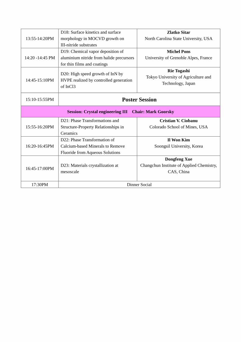
13:55-14:20PM
D18: Surface kinetics and surface
morphology in MOCVD growth on
III-nitride substrates
Zlatko Sitar
North Carolina State University, USA
14:20 -14:45 PM
D19: Chemical vapor deposition of
aluminium nitride from halide precursors
for thin films and coatings
Michel Pons
University of Grenoble Alpes, France
14:45-15:10PM
D20: High speed growth of InN by
HVPE realized by controlled generation
of InCl3
Rie Togashi
Tokyo University of Agriculture and
Technology, Japan
15:10-15:55PM Poster Session
Session: Crystal engineering III Chair: Mark Goorsky
15:55-16:20PM
D21: Phase Transformations and
Structure-Property Relationships in
Ceramics
Cristian V. Ciobanu
Colorado School of Mines, USA
16:20-16:45PM
D22: Phase Transformation of
Calcium-based Minerals to Remove
Fluoride from Aqueous Solutions
Il Won Kim
Soongsil University, Korea
16:45-17:00PM D23: Materials crystallization at
mesoscale
Dongfeng Xue
Changchun Institute of Applied Chemistry,
CAS, China
17:30PM Dinner Social
Wednesday Dec. 16
Room B
7:00-8:00AM Breakfast
Session: Radiation Detector Materials - From Crystal Growth to Device Applications II
Chair: HongJoo Kim
8:00-8:25AM
B27: Facile fabrication of porphyrin
Janus particles from water droplet
template at oil-aqueous interface
Jingxia Wang
Technical Institute of Physics and
Chemistry, China
8:25-8:50AM
B28: GaSb alternative substrates for
MBE growth of next generation HgCdTe
infrared detectors
Wen Lei
University of Western Australia, Australia
Session: III-Nitrides for Lighting, Photovoltaics and Sensing Applications III
Chair: Yasushi Nanishi
8:50-9:15AM
B29: Preparation of III-Nitride Devices
for Large Area Light Emitting Devices
and Solar Cells
Hiroshi Fujioka
The University of Tokyo, Japan
9:15-9:40AM
B30: Recent Advances in Basic
Ammonothermal Growth of Gallium
Nitride
Siddha Pimputkar
University of California, USA
9:40-10:05AM B31: InGaN pyramidal quantum dot as a
source of single photons
Houssaine Machhadani
Linköping University, Sweden
10:05-10:20AM Session Break
Session: Crystal engineering IV Chair: Zhipeng Guo
10:20-10:45AM
B32: Layer crystal growth with fractal
analysis technique: from theory to
engineering application
Xiaobin Jiang
Dalian University of Technology, China
10:45-11:10AM B33: Engineering Functional Materials by
Halogen Bonding
Giancarlo Terraneo
Politecnico di Milano, Italy
11:10-11:35AM
B34: Crystal growth control in
chalcogenide and its application to
multilevel storage in phase-change
memory
You Yin
Gunma University, Japan
12:00-13:30 PM Lunch Break
Session: Epitaxial thin films and nanostructures VI Chair: Sylke Blumstengel
13:30-13:55PM
B35: Monolithic integrated Ge light
emitters fabricated by epitaxial lateral
overgrowth
Katsuya Oda
Hitachi Ltd., Research & Development
Group, Japan
13:55-14:20PM
B36: Atomically Engineered
Metal-Insulator Transition at the
TiO2/LaAlO3 Heterointerface
Makoto Minohara
High Energy Accelerator Research
Organization (KEK), Japan
14:20 -14:45 PM
B37: Thermodynamics and kinetics of
nanocluster formation on semiconductor
surfaces
Andreas Fissel
Leibniz University Hannover, Germany
14:45-15:10PM B38: Epitaxial growth of metastable
oxide thin films under atmosphere
Kentaro Kaneko
Kyoto University, Japan
15:10-15:25PM Session Break
Session: Epitaxial thin films and nanostructures VII Chair: Hans Von Känel
15:25-15:45PM
B39: Growth and Characterization of Full
Flux-closure Quadrants in PbTiO3 thin
films
Yinlian Zhu
Institute of Metal Research, CAS, China
15:45-16:10PM
B40: Synthesis of Polar and Non-Polar
Epitaxial GaN Thin Films by Ion-Beam
Nitridation of Ga Droplets
Jürgen W. Gerlach
Leibniz Institute of Surface Modification
(IOM), Germany
16:10-16:35PM
B41: Epitaxial growth of hybrid
inorganic/organic semiconductor
structures
Sylke Blumstengel
Humboldt-Universität zu Berlin, Germany
16:35-17:00PM
B42: Epitaxially stabilized oxide film
composed of twisted triangular-lattice
layers
Masaki Uchida
The University of Tokyo, Japan
17:00-17:25PM
B43: Growth temperature dependence of
crystalline state of
low-temperature-grown InGaAs on InP
substrate
Yoriko Tominaga
Hiroshima University, Japan
17:30PM Dinner Social
Wednesday Dec. 16
Room C
7:00-8:00AM Breakfast
Session: General V Chair: Jean-Noel Aqua
8:00-8:25AM
C24: Supercooled liquids, glasses and
growth of dendrites under out of
equilibrium conditions
Francesco Aliotta
Istituto per I Processi Chimici-Fisici, CNR
Italy
8:25-8:50AM
C25: Electric Field Assisted Growth of
Organic Conductive wire and
Self-aligned Organic Nanotransistor
Masatoshi Sakai
Chiba University, Japan
8:50-9:15AM C26: Calcium minerals crystal growth
for dental material applications
Yuki Sugiura
Kyushu University, Japan
9:15-9:40AM C27: Morphology effect on the
nano-hematite and its magnetic property
Yen-Hua Chen
National Cheng Kung University, Taiwan
9:40-10:05AM
C28: Dynamics of Multi-functional
Materials with Inelastic Neutron
Scatterings
Dehong Yu
Australian Nuclear Science and Technology
Organisation, Australia
10:05-10:20AM Session Break
Session: General VI Chair: Alexander Gelfgat
10:20-10:45AM
C29: Structural diversity of
multi-component self-assembled
systems
Irene Ling
University of Malaya, Malaysia
10:45-11:10AM C30: Magnetocaloric effect in
multifunctional perovskites
Suja Elizabeth
Indian Institute of Science, India
11:10-11:35AM
C31: Strain-engineered SiGe
nanomembranes on Porous Silicon
stressor
Jean-Noel Aqua
Université Paris 6 – INSP, France
11:35-12:00PM C32: Silicon Nanostructures for
Nanoelectronics and Photovoltaics
Noushine Shahidzadeh
University of Amsterdam, The Netherlands
12:00-13:30 PM Lunch Break
Session: Crystal engineering V Chair: Guy Chichignoud
13:55-14:20PM
C33: Morphology Control of Metal
Oxide Crystals for Multifunctional
Cosmetic Application
Tsugio Sato
Tohoku University, Japan
14:20-14:45PM C34: Crystal engineering of cocrystals:
air-stable cyclohexasulfur as cocrystal
Kunihisa Sugimoto
Japan Synchrotron Radiation Research
Institute(JASRI), Japan
14:45 -15:10PM C35: Drug beneficiation via
cyclodextrin inclusion
Mino R. Caira
University of Cape Town, South Africa
15:10-15:25PM Session Break
Session: Crystal engineering VI Chair: Kader Zaidat
15:25 -15:50PM
C36: The discrete crystal growth:
multi-scale phenomena, mechanism and
influence on segregation
Xiaoping Ma
Institute of Metal Research, CAS, China
15:50-16:15PM
C37: In Situ Study of the Crystal
Formation Process of Molecular
Materials
Yang Liu
Shandong University, China
16:15-16:40PM
C38: Wetting and joining of structural
materials by growth of metal borates
nano/micro whiskers
Jian Cao
Harbin Institute of Technology, China
17:30PM Dinner Social
Wednesday Dec. 16
Room D
7:00-8:00AM Breakfast
Session: Epitaxial thin films and nanostructures VIII Chair: Kosuke Matsuzaki
8:00-8:25AM
D24: Growth of strained Si/SiGe on
Si(110) substrates for realization of
high-mobility devices
Keisuke Arimoto
University of Yamanashi, Japan
8:25-8:50AM
D25: Construction of well-defined 3D
transition metal oxides nanostructures
and their novel properties
Azusa N. Hattori
Osaka University, Japan
8:50-9:15AM D26: A-site driven ferroelectricity in
strained La2NiMnO6 thin films
Ryota Takahashi
University of Tokyo, Japan
9:15-9:40AM
D27: Synthesis of
Heteroatom-Containing Nanocarbon
Materials by Solution Plasma Process
in Organic Solution
Takahiro Ishizaki
Shibaura Institute of Technology, Japan
9:40-10:05AM D28: Modified InAs/GaAs quantum
dots for enhanced solar cell efficiency
Jose María Ulloa
Universidad Politécnica de Madrid, Spain
10:05-10:20AM Session Break
Session: Epitaxial thin films and nanostructures IX Chair: Masaki Uchida
10:20-10:45AM
D29: Low Temperature Deposition of
Epitaxial (K,Na)NbO3 Films using
Hydrothermal Method
Takahisa Shiraishi
Tohoku University, Japan
10:45-11:10AM D30: Epitaxial Growth of InAs-based
Quantum Structures on GaAs
Itaru Kamiya
Toyota Technological Institute, Japan
11:10-11:35AM D31: Epitaxial growth of bipolar
conducting Cu3N (100) thin films
Kosuke Matsuzaki
Tokyo Institute of Technology, Japan
11:35-12:00PM
D32: A-axis Growth of nano
structured VO2 Thin films by Pulsed
Laser Deposition on substrate glass
Balla Diop Ngom
Universit Cheikh Anta Diop de Dakar
(UCAD), Senegal
12:00-13:30PM Lunch Break
Session: General VII Chair: Masaharu Oshima
13:55-14:20PM
D33: Non-intrusive instability
measurements in a model of
Czochralski melt flow
Alexander Gelfgat
Tel Aviv University, Israel
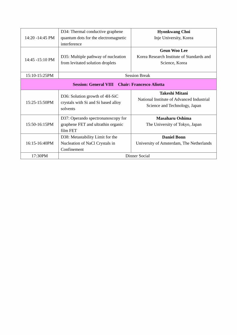
14:20 -14:45 PM
D34: Thermal conductive graphene
quantum dots for the electromagnetic
interference
Hyonkwang Choi
Inje University, Korea
14:45 -15:10 PM D35: Multiple pathway of nucleation
from levitated solution droplets
Geun Woo Lee
Korea Research Institute of Standards and
Science, Korea
15:10-15:25PM Session Break
Session: General VIII Chair: Francesco Aliotta
15:25-15:50PM
D36: Solution growth of 4H-SiC
crystals with Si and Si based alloy
solvents
Takeshi Mitani
National Institute of Advanced Industrial
Science and Technology, Japan
15:50-16:15PM
D37: Operando spectronanoscopy for
graphene FET and ultrathin organic
film FET
Masaharu Oshima
The University of Tokyo, Japan
16:15-16:40PM
D38: Metastability Limit for the
Nucleation of NaCl Crystals in
Confinement
Daniel Bonn
University of Amsterdam, The Netherlands
17:30PM Dinner Social
Tuesday Dec. 15
15:10-15:55PM
Poster Session
P01 Electrical and optical properties of ZnO films