PANTEL ET AL . VOL. 5 ’ NO. 7 ’ 6032–6038 ’ 2011 www.acsnano.org 6032 June 20, 2011 C 2011 American Chemical Society Room-Temperature Ferroelectric Resistive Switching in Ultrathin Pb(Zr 0.2 Ti 0.8 )O 3 Films Daniel Pantel, * Silvana Goetze, Dietrich Hesse, and Marin Alexe Max Planck Institute of Microstructure Physics, Weinberg 2, 06120 Halle (Saale), Germany D ue to their switchable spontaneous polarization, ferroelectric materials can be used as nonvolatile mem- ories, e.g., ferroelectric random access mem- ories (FeRAM), but so far their destructive readout scheme limits the applications of ferroelectric memories. 1,2 Evaluating the polarization direction by a nondestructive readout scheme rather than by the switched charge would be a tremendous advantage. This has been recognized al- ready from the early time of ferroelectric memories by development of the most simple nonvolatile memory cell: the ferro- electric field effect transistor (FeFET). 3,4 The major yet unsolved problem of FeFET is the low retention time, i.e., the time within which the written information vanishes and the two polarization directions become indistinguishable. Losing information is most probably caused by the strongly asym- metric metalferroelectricsemiconductor structure, which generates polarization back-switching. Therefore, it will be highly desirable to find an alternative route to read nondestructively the polarization in a sim- ple metalferroelectricmetal (MFM) struc- ture, similar to the polar switch proposed by Esaki and co-workers. 5 The leakage current in usual thin film ferroelectric capacitors is mostly governed by the band alignment at the metalferro- electric interface, the potential barrier, which itself is influenced by the polarization state. 6,7 Thus the effective resistance of a ferroelectric memory cell would have two bistable states like in resistive switching ran- dom access memories (RRAMs). In RRAMs these resistive effects are usually based on defects or on chemical processes 8,9 that may be difficult to control during the fabri- cation process. 10 On the contrary the resis- tive switching based on polarization switching in ferroelectrics is in principle a pure elec- tronic process, and this might alleviate these drawbacks. Furthermore, ferroelectric polarization and thus the information stored in a memory cell can in principle be switched in the picosecond range, 11,12 as the effective switching time is usually lim- ited only by the electrical circuit. 11,13 Following this route, resistive switching in ferroelectrics has been intensively investi- gated in bulk crystals, 14 organic films, 1517 and thin oxide films. 10,1827 In this frame- work Maksymovych et al., 21 using a conduc- tive atomic force microscope (AFM) tip as a top electrode, showed that indeed the polarization direction influences FowlerNordheim tunneling into ferroelectrics. Nevertheless, for application in memory cells a real metalferroelectricmetal het- erostructure, i.e., a capacitor, is required. The capacitor geometry would exclude any spurious effects on the resistance due, for instance, to electrochemical interaction between the AFM tip and the ferroelectric surface. 2830 Furthermore, the uniform electric field in the case of a capacitor-like geometry provides better physical insight into the switching and transport mechanism. 31 * Address correspondence to [email protected]. Received for review May 20, 2011 and accepted June 19, 2011. Published online 10.1021/nn2018528 ABSTRACT Spontaneous polarization of ferroelectric materials has been for a long time proposed as binary information support, but it suffers so far from destructive readout. A nondestructive resistive readout of the ferroelectric polarization state in a me- talferroelectricmetal capacitor would thus be advantageous for data storage applications. Combing conducting force microscopy and piezoelectric force microscopy, we unambiguously show that ferroelectric polarization direction and resistance state are correlated for epitaxial ferroelectric Pb(Zr 0.2 Ti 0.8 )O 3 nanoscale capacitors prepared by self-assembly methods. For intermediate ferro- electric layer thickness (∼9 nm) sandwiched between copper and La 0.7 Sr 0.3 MnO 3 electrodes we achieved giant electroresistance with a resistance ratio of >1500 and high switching current densities (>10 A/cm 2 ) necessary for effective resistive readout. The present approach uses metalferroelectricmetal devices at room temperature and, therefore, significantly advances the use of ferroelectric-based resistive switching. KEYWORDS: ferroelectrics . resistive switching . nanoscale capacitor . conductive-AFM . PFM . Pb(Zr 0.2 Ti 0.8 )O 3 ARTICLE
Transcript
PANTEL ET AL . VOL. 5 ’ NO. 7 ’ 6032–6038 ’ 2011
www.acsnano.org
6032
June 20, 2011
C 2011 American Chemical Society
Room-Temperature FerroelectricResistive Switching in UltrathinPb(Zr0.2Ti0.8)O3 FilmsDaniel Pantel,* Silvana Goetze, Dietrich Hesse, and Marin Alexe
Max Planck Institute of Microstructure Physics, Weinberg 2, 06120 Halle (Saale), Germany
Due to their switchable spontaneouspolarization, ferroelectric materialscan be used as nonvolatile mem-
ories, e.g., ferroelectric randomaccessmem-ories (FeRAM), but so far their destructivereadout scheme limits the applications offerroelectric memories.1,2 Evaluating thepolarization direction by a nondestructivereadout scheme rather than by theswitched charge would be a tremendousadvantage. This has been recognized al-ready from the early time of ferroelectricmemories by development of the mostsimple nonvolatile memory cell: the ferro-electric field effect transistor (FeFET).3,4 Themajor yet unsolved problem of FeFET is thelow retention time, i.e., the time withinwhich the written information vanishesand the two polarization directions becomeindistinguishable. Losing information ismost probably caused by the strongly asym-metric metal�ferroelectric�semiconductorstructure, which generates polarizationback-switching. Therefore, it will be highlydesirable to find an alternative route to readnondestructively the polarization in a sim-ple metal�ferroelectric�metal (MFM) struc-ture, similar to the polar switch proposed byEsaki and co-workers.5
The leakage current in usual thin filmferroelectric capacitors is mostly governedby the band alignment at the metal�ferro-electric interface, the potential barrier,which itself is influenced by the polarizationstate.6,7 Thus the effective resistance of aferroelectric memory cell would have twobistable states like in resistive switching ran-dom access memories (RRAMs). In RRAMsthese resistive effects are usually based ondefects or on chemical processes8,9 thatmay be difficult to control during the fabri-cation process.10 On the contrary the resis-tive switching based onpolarization switchingin ferroelectrics is in principle a pure elec-tronic process, and this might alleviate
these drawbacks. Furthermore, ferroelectricpolarization and thus the informationstored in a memory cell can in principle beswitched in the picosecond range,11,12 asthe effective switching time is usually lim-ited only by the electrical circuit.11,13
Following this route, resistive switching inferroelectrics has been intensively investi-gated in bulk crystals,14 organic films,15�17
and thin oxide films.10,18�27 In this frame-work Maksymovych et al.,21 using a conduc-tive atomic force microscope (AFM) tip asa top electrode, showed that indeed thepolarization direction influences Fowler�Nordheim tunneling into ferroelectrics.Nevertheless, for application in memorycells a real metal�ferroelectric�metal het-erostructure, i.e., a capacitor, is required.The capacitor geometry would excludeany spurious effects on the resistance due,for instance, to electrochemical interactionbetween the AFM tip and the ferroelectricsurface.28�30 Furthermore, the uniformelectric field in the case of a capacitor-likegeometry provides better physical insightinto theswitchingand transportmechanism.31
Electroresistance effects have been found in ferroelec-tric thin films with real metal electrodes,10,24,26,27 but itis not yet unambiguously shown that these effects aresolely based on the ferroelectric switching.Here, we apply a self-assembly approach to prepare
large arrays of well-ordered ferroelectric capacitorswith typical sizes smaller than 0.1 μm2.We clearly showthe direct correlation between polarization switchingand resistive switching in MFM heterostructures withultrathin epitaxial ferroelectric lead zirconate titanate,Pb(Zr0.2Ti0.8)O3 (PZT), films by measuring the currentthrough a gold-capped Cu/PZT/La0.7Sr0.3MnO3 (LSMO)capacitor with a ca. 9 nm thick ferroelectric PZT layerand the polarization direction using conducting forcemicroscopy (C-AFM) and piezoelectric force micro-scopy (PFM), respectively.Ferroelectric PZT was chosen as a model room-
temperature ferroelectric material that can be epitaxi-ally grown, almost defect free, on SrTiO3 (STO) sub-strates, giving a high spontaneous polarization,32 andcan evenbe integrated onto silicon.33 Usual ferroelectriccapacitors have a typical electrode area on the order ofseveral tens or hundreds of square micrometers, andusually the defect-mediated leakage paths will rule theoverall current and obscure the polarization-dependentcurrent for ultrathin ferroelectric films. In order to avoidthis, submicrometer capacitors have to be used.We use natural lithography34 or nanosphere litho-
graphy (NSL)35,36 to fabricate arrays of well-orderednanoscale ferroelectric capacitors. NSL is a versatilelithography technique producing well-ordered maskswith scalable pitch and feature size relying on the self-assembly of a mono or double layer of hexagonallyclose-packed polystyrene latex spheres.34�36 First itwas applied to produce ordered arrays ofmetal nanois-lands, but later on also to the growth of ordered 1Dnanostructures,37 ferroelectric nanodots,38 magneticnanodots,39 and organic semiconductor particles.35
Here, we use nanosphere lithography to producearrays of well-ordered metal electrodes on the topferroelectric surface.
RESULTS AND DISCUSSION
The MFM preparation process is sketched in Figure1a. First, the oxide layers were grown by pulsed laserdeposition (PLD) at elevated temperature. Directlyafter cooling, the samples were removed from thePLD chamber and NSL was applied. Details of theNSL process can be found in the Methods section.The self-assembled monolayer of polystyrene latexspheres (1 μm diameter) was subsequently used as astencil mask for thermal evaporation of the metallayers (here Cu capped with Au). Figure 1b shows theperfect self-assembly of the spheres into a monolayeron the PZT surface after metal deposition. Copper waschosen as the top electrode since it gives good Schottkybarriers with PZT.40 The resulting well-ordered metalnanostructures (Figure 1c) were obtained by dissolvingthe latex nanospheres in dichlormethane.Transport and piezoelectric measurements are then
performed by contacting the nanoscale top electrodeusing anAFM tip (schematically sketched in the inset ofFigure 3) through which IV curves (C-AFM mode) andpiezoelectric characteristics (PFM) are measured.For the present Cu/PZT/LSMO heterostructures, two
issues in terms of film quality need to be addressed tounambiguously analyze measured transport datathrough ultrathin ferroelectric films. First, the LSMObottom electrode needs to be almost perfect in termsof the structural quality and surface morphology. Anatomically flat surface is necessary to avoid any currentinhomogeneity. Second, one needs to have an effec-tive resistance much smaller than the junction resis-tance to avoid current limiting by a parasitic serialresistance. Thus the actual resistivity needs to be as lowas possible, and a high enough LSMO thickness toensure a low effective resistance is necessary. Theoptimum thickness of the LSMO bottom electrodewas found to be around 50 nm with its typical proper-ties being shown in the Supporting Information.Another important issue is the PZT polarization,
since the electroresistance scales exponentially withpolarization value.41 It is known that polarization
Figure 1. (a) Schematic of the NSL process adapted for nanoscale electrode preparation on PZT surfaces. (b) Scanningelectron microscopy (SEM) image of a hexagonally close packed monolayer of polysterene spheres and (c) the resultingAu-capped Cu nanoislands (by AFM) on top of a PZT surface.
ARTIC
LE
PANTEL ET AL . VOL. 5 ’ NO. 7 ’ 6032–6038 ’ 2011
www.acsnano.org
6034
decreases as the film thickness decreases below10 nm.42�45 We have shown that a very high electro-resistance is given by the thermionic injection(Schottky) transport mechanism or by changing thetransport mechanism from thermionic injection toFowler�Nordheim tunneling by polarization direc-tion.31 The thickness range where this is suitable interms of low voltage and sufficiently high currentdensity is rather narrow. For PZT the optimum thick-ness will be approximately in the range of 4 to 10 nm.Indeed, for a 20 nm thick PZT film almost no currentcan be measured for voltages below coercive voltage.For the present case the ferroelectricity was con-
firmedbyPFM for thefilms thinner than10nm. Figure 2ashows poling experiments on a bare PZT surface for theprimarily investigated 9 nm thick PZT film. In the as-grown state the polarization points upward, i.e., towardthe AFM tip, like in the case of a positively poledsurface. The poled ferroelectric domain configurationis stable for at least several hours. Thicker PZT films(20 nmormore) grown at the same conditions showonmacroscopic capacitors (0.04 mm2) fully saturatedferroelectric polarization loops with a high remnantpolarizationof about 110μC/cm2 (Supporting Information),confirming the excellent ferroelectric properties of ourPZT films.32 The high remnant polarization is in agree-ment with the large out-of-plane lattice constant re-sulting from the in-plane compressive stress from theSTO substrate of the PZT layers, as shown by X-rayinvestigations. All our heterostructures are grownfully strained to the STO lattice, as confirmed byreciprocal space mappings around the STO 203
reflection (Supporting Information), ensuring high po-larization even for ultrathin films. High-resolutiontransmission electron microscope images (Figure 2b)indicate coherent growth with sharp interfaces.Figure 3a shows IV characteristics of a 1.5 μm2 and a
0.04 μm2 Au-capped Cu electrode on top of a 9 nmthick PZT film. A large hysteresis in current is observedfor both devices. It is worth noting that devices with alarge difference in area show similar current densities(see also Figure S4 in Supporting Information), which isa strong indication for a homogeneous transport overthe electrode area, in contrast to a filament- or defect-controlled transport. By running fromþ3 V to�3 V, thecurrent switches from the low conducting state (OFF)to thehigh conducting state (ON) at approximately�2.1 Vand back to the OFF state at about 0.8 V whensweeping from �3 V to þ3 V, as the polarizationpresumably switches. The switching voltage variesslightly from device to device. The OFF state is forthe polarization up and the ON state is for polariza-tion down, with the as-grown state being OFF, inagreement with the as-grown upward polarizationdirection deduced from Figure 2a. The displacementcurrent peaks, clearly visible in Figure S3a, cannot beseen here because of the long measurement timeas well as the low expected current density com-pared to the current density in the ON state. Theswitching behavior is observed for most of theinvestigated devices, although some show high,not switchable leakage, probably because of con-ducting paths due to clustering of defects under-neath those electrodes.
Figure 2. (a) Topographic and piezoresponse AFM imagesof a ca. 9 nm thick epitaxial PZTfilm after poling two squaresin an as-grown regionwith a voltageof�2V (2� 2 μm2) andþ2V (1� 1 μm2) appliedbetweenbottomelectrode and theconductive AFM tip. A PFM-phase change by 180� with noobservable topographic change confirms the ferroelectricnature of the PZT film. (b) HR-TEM micrograph of the samePZT/LSMO/STO heterostructure.
Figure 3. (a) Current density j versus voltage V on a 1.5 μm2
and a 0.04 μm2 Cu/Au island on a ca. 9 nm thick PZT filmmeasured by different conductive coating of AFM tips(Ti�Pt and conductive diamond, respectively) as sketchedin the inset, demonstrating that electrode size and tip donot influence the result. (b) Electroresistance ER and ON/OFF ratio versus operation voltage V calculated for the1.5 μm2 device from (a). All lines are guides to the eye.
ARTIC
LE
PANTEL ET AL . VOL. 5 ’ NO. 7 ’ 6032–6038 ’ 2011
www.acsnano.org
6035
The electroresistance (ER) is given by
ER ¼ j(PV,ON) � j(Pv,OFF)
j(PV,ON)(1)
where j is the current density, which approaches in ourcase unity; that is, the ratio between ON and OFF statesexceeds about 100, at reasonable operation voltagesbelow the switching voltage (see Figure 3b). However,the ON/OFF ratio rises to 1500 (at�1.3 V), being higherthan in C-AFM based reports,23,20,22 as expected by thethickness dependence of the electroresistance.31,23
The switched current density exceeds 10 A/cm2 atvoltages below the switching voltage, higher than inPt/BiFeO3/SrRuO3 heterostructures with much thickerferroelectric layers.10
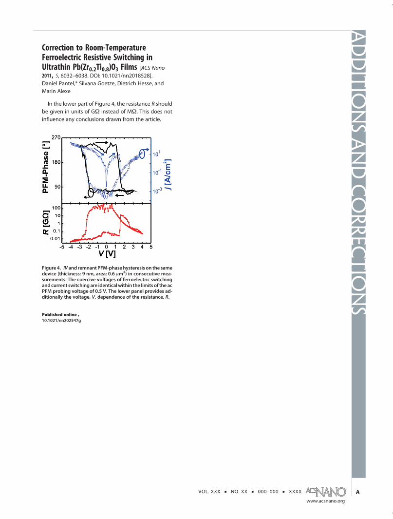
To establish a direct correlation between ferroelec-tric and resistive switching, simultaneous or consecu-tive measurements of the voltage dependence of aferroelectric parameter, e.g., polarization, and the cur-rent on the same device are necessary.19,21 Here, weconsecutively measure the IV characteristics and thenthe piezoelectric loop on the same capacitor (Figure 4).The IV characteristics show switching voltages of ap-proximately 1.4 and �2.2 V. As expected, for ferro-electric polarization switching, the PFM phase changesby 180� at the coercive voltages (1.4 and �2.2 V,corresponding to a coercive field of about 2 MV/cm,on the order of what is observed in ultrathin ferro-electric films21�23); that is, the coercive voltage and thevoltage at which the resistance switches coincide.Therefore we conclude that the resistive switching isoriginating in ferroelectric switching. Due to the smallsize of the electrodes and the low currents, heatingeffects of the tip are negligible.19 Hence, we do not seethat thecurrent influences thepiezoelectricmeasurements.
Retention is an important issue for the nonvolatilememory cells, which in the case of ferroelectric mem-ories is due to polarization back-switching or imprintphenomena.2 In the present case retention providesadditional evidence for the ferroelectric origin of theresistive switching. Some electrodes show stable cur-rent states of the negatively poled state (ON state,polarization down) for more than one hour (Figure 5a).However, few devices (see Figure 5b) show rapid back-switching of the polarization from down to up asobserved in the PFM-phase signal by a change of180� after several 10 seconds. As shown in Figure 5b,the current density of the same electrodes decays on asimilar time scale, which is in agreement with a polar-ization back-switching scenario. This observation ex-cludes any voltage-driven electrochemical effects onthe resistive switching, since during polarization andresistive back-switching there is no electrical fieldapplied. The rather broad transition in current com-pared to the switching in PFM phase is mostly due tothe difference in the effect of polarization switching onthe mechanical behavior (vibrations by piezoelectriceffect) and the electronic conduction: The polarizationswitching proceeds by nucleation and growth even fornanoscale capacitors,46 which means that at certainstages during the back-switching the capacitor willconsist of domains with different orientations. Whilethe phase switches by 180� when more than 50% ofthe area is switched, the influence of the polarization
Figure 4. IV and remnant PFM-phase hysteresis on the samedevice (thickness: 9 nm, area: 0.6 μm2) in consecutivemeasurements. The coercive voltages of ferroelectricswitching and current switching are identical within thelimits of the ac PFM probing voltage of 0.5 V. The lowerpanel provides additionally the voltage, V, dependence ofthe resistance, R. Figure 5. (a) Retentionproperties of a typical capacitor after
switching with �2.5 V recorded at �1.7 V, demonstrating along retention time. The error bars indicate the currentfluctuations during the measurement. Other capacitorshave smaller retention times, as shown in (b). The timedependencyof the PFMphase after switchingwith(3V andthe current state at�1V after switchingwith�3V show thatback-switching of the polarization from down to up occurson the same time scale as the transition from high to lowconduction state. All lines are guides to the eye.
ARTIC
LE
PANTEL ET AL . VOL. 5 ’ NO. 7 ’ 6032–6038 ’ 2011
www.acsnano.org
6036
on the current is exponential andmay lead to an earlierchange in current during polarization back-switching.One of the most important questions is related to
the transport mechanism that governs the electrore-sistance. As the ferroelectric films are relatively thick(9 nm), direct tunneling is rather unlikely. For theinvestigated ferroelectric barrier thickness thermionicinjection is expected to prevail on the electronictransport at room temperature.31 The correspondingelectric field (E) dependency of the current density(jSchottky) for simple semiconductors is given by47
jSchottky ¼ A��T2 exp � 1
kBTΦB �
ffiffiffiffiffiffiffiffiffiffiffiffiffiffiffie3E
4πε0εifl
s0@
1A
24
35(2)
with temperature T, the effective Richardson's constantA**, the image force lowering permittivity εifl, and thepotential barrier ΦB. The electric field E for a ferro-electric material is a superposition of the applied field,the depolarization field, and the field due to the bandalignment.7 In the Supporting Information (Figure S5),we show a fit of the obtained IV data to eq 2, fromwhich we conclude that indeed thermionic injection
dominates the transport for the investigated film. Theobtained changes in barrier heights from 0.57 and0.67 eV in the ON state to 1.33 and 0.63 eV in theOFF state are consistent with the electrostatic modelfor the dependence of an asymmetric barrier on thepolarization direction of a metal�ferroelectric�metalheterostructure.41
Higher currents necessary for the use of low-costcurrent amplifiers in memory applications9,10 can beachieved in high-quality ferroelectric films with thick-nesses below about 4 nm by tunneling,31 which alsoprovides electroresistance,48,41,20 or by using semicon-ductor ferroelectrics.10
CONCLUSIONS
In summary, we have shown an approach to preparenanoscalemetal�ferroelectric�metal capacitors usingself-assemblymethods. These nanoscale capacitors aresubsequently used to clearly show the direct correla-tion between resistive and ferroelectric switching inultrathin PZT films. A high resistance ratio, up to 1500,as well as high switched current densities of about10 A/cm2 open new pathways toward ferroelectricity-based nonvolatile memory devices.
METHODSSample Preparation. PLD was performed at substrate tem-
peratures between 550 and 600 �C in an oxygen atmosphereof 0.2 mbar ablating stoichiometric ceramic targets (with 10%Pb excess for the PZT target). Base pressure of our PLD system isbelow 5 � 10�6 mbar. The energy fluence of the KrF excimerlaser (λ = 248 nm) at the target was about 300 mJ/cm2. The 0.1�off-cut STO (100)-oriented substrates were etched and an-nealed before deposition to obtain an atomically flat, singleTiO2-terminated surface with approximately 200 nm wideterraces separated by one unit cell high steps.49
For NSL a commercial water solution of monodispersepolysterene latex spheres (2.5 wt %) was diluted 1:1 by volumewith isopropyl alcohol (p.a.) to reduce surface tension. For the1 μm diameter spheres, 5 μL of the obtained solution wasdripped on the approximately 10� tilted sample surface anddried at room temperature. More details on NSL can be found inthe Supporting Information.
For thermal evaporation, the Cu and Au were evaporatedfrom a tungsten coil and boat, respectively, at a distance of10 cm from the sample. The sample could bemoved to allow formetal heterostructures with the thicknesses controlled by aquartz crystal. The pressure during the room-temperature deposi-tion process was kept below 7� 10�6 mbar to prevent oxidation.
Piezoelectric Force and Conductive Scanning Probe Microscopy. TheAFM-based investigations were carried out using a CP-Researchmicroscope (Thermomicroscope) with a variety of conductiveAFM tips (ATEC-EFM/Ir�Pt, NSC15/Ti�Pt, DDESP-FM/dopeddiamond, CDT-FMR/doped diamond) in contact mode. A lock-in amplifier (SR 830 DSP) was used to apply the ac probingvoltage (f = 24.5 kHz) with an amplitude of 0.5 V, well belowthe coercive voltage of the PZT films, to the bottom electrodeand to measure the piezoresponse signal. Direct currentvoltage pulses were also superimposed for remnant hyster-esis measurements by the lock-in amplifier, where the piezo-response was measured at Vdc = 0 V after poling with an appliedvoltage for 200 ms.
For collecting IV curves the measured current was amplifiedby 108 V/A with a variable gain sub femto ampere currentamplifier (Femto DDCPA-300) and subsequently by �10 (low-noise preamplifier, SR 560) and filteredwith a lowpass filter (1 kHz).The resulting voltage, proportional to the current, was mea-sured by a KeithleyMultimeter 2000. The IVmeasurement setupwas previously calibrated using a Keithley Electrometer 6517Bconnected to the tip. A 1 MΩ serial resistor limited the currentthrough theAFM tip. A full voltage sweep took about 10 s, i.e., onthe same time scale as the PFM loops.
For the retention measurement the polarization wasswitched by a voltage pulse (�3 V, 1 s) into a defined polariza-tion state. Consecutively, the voltage was held at 0 V. Tomeasure the current after a certain retention time, the voltagewas set to�1 V, and after 1 s (to let the current relax into a stablestate) the current was measured.
Transmission Electron Microscopy. High-resolution TEM investi-gations were performed using a Jeol 4010 microscope. TEMsamples were prepared by standard methods (mechanicalpolishing and ion milling).
Acknowledgment. This work has been supported by theGerman Science Foundation (DFG) through SFB762. We arethankful to N. Schammelt for PLDmaintenance and to P.Wernerfor helpwithHR-TEM.We thank Y. Kim for useful discussions andO. Moutanabbir for carefully reading the manuscript.
Supporting Information Available: Details for NSL, LSMOproperties, PZT properties, additional electrical measurementson nanoscale capacitors, and fits of the IV curves to thethermionic injection model. This material is available free ofcharge via the Internet at http://pubs.acs.org.
REFERENCES AND NOTES1. Auciello, O.; Scott, J. F.; Ramesh, R. The Physics of Ferro-
electric Memories. Phys. Today 1998, 51, 22–27.2. Scott, J. Ferroelectric Memories; Springer: Berlin, 2000.
ARTIC
LE
PANTEL ET AL . VOL. 5 ’ NO. 7 ’ 6032–6038 ’ 2011
www.acsnano.org
6037
3. Looney, D. H.; Summit, N. J. Semiconductive TranslatingDevice. US Patent 2,791,758, 1957.
4. Wu, S.-Y.; Francombe, M. H. Ferroelectric Memory Device.US Patent 3,832,700, 1974.
5. Esaki, L.; Laibowitz, R.; Stiles, P. Polar Switch. IBM Tech.Disclosure Bull. 1971, 13, 2161.
6. Chang, L.; Esaki, L. Nonvolatile Schottky Diode with BarrierHeight Controlled by Ferroelectric Polarization. IBM Tech.Disclosure Bull. 1971, 14, 1250–1251.
10. Jiang, A. Q.; Wang, C.; Jin, K. J.; Liu, X. B.; Scott, J. F.; Hwang,C. S.; Tang, T. A.; Liu, H. B.; Yang, G. Z. A Resistive Memory inSemiconducting BiFeO3 Thin-Film Capacitors. Adv. Mater.2011, 23, 1277–1281.
11. Li, J.; Nagaraj, B.; Liang, H.; Cao, W.; Lee, C. H.; Ramesh, R.Ultrafast Polarization Switching in Thin-Film Ferroelectrics.Appl. Phys. Lett. 2004, 84, 1174–1176.
12. Korff Schmising, C. v.; Bargheer, M.; Kiel, M.; Zhavoronkov,N.; Woerner, M.; Elsaesser, T.; Vrejoiu, I.; Hesse, D.; Alexe, M.Coupled Ultrafast Lattice and Polarization Dynamics inFerroelectric Nanolayers. Phys. Rev. Lett. 2007, 98, 257601.
13. Jiang, A. Q.; Lin, Y. Y.; Tang, T. A. Interfacial-Layer Modula-tion of Domain Switching Current in Ferroelectric ThinFilms. J. Appl. Phys. 2007, 101, 104105.
15. Qu, H.; Yao, W.; Garcia, T.; Zhang, J.; Sorokin, A. V.; Ducharme,S.; Dowben, P. A.; Fridkin, V. M. Nanoscale PolarizationManipulation and Conductance Switching in Ultrathin Filmsof a Ferroelectric Copolymer. Appl. Phys. Lett. 2003, 82,4322–4324.
16. Asadi, K.; de Leeuw, D. M.; de Boer, B.; Blom, P. W. M.Organic Non-Volatile Memories from Ferroelectric Phase-Separated Blends. Nat. Mater. 2008, 7, 547–550.
17. L�opez-Encarnaci�on, J. M.; Burton, J. D.; Tsymbal, E. Y.; Velev,J. P. Organic Multiferroic Tunnel Junctions with Ferro-electric Poly(vinylidene fluoride) Barriers. Nano Lett.2011, 11, 599–603.
18. Shen, W.; Dittmann, R.; Breuer, U.; Waser, R. Improved Endur-ance Behavior of Resistive Switching in (Ba,Sr)TiO3 Thin Filmswith W Top Electrode. Appl. Phys. Lett. 2008, 93, 222102–3.
19. Kohlstedt, H.; Petraru, A.; Szot, K.; Rudiger, A.; Meuffels, P.;Haselier, H.; Waser, R.; Nagarajan, V. Method to DistinguishFerroelectric from Nonferroelectric Origin in Case of Re-sistive Switching in Ferroelectric Capacitors. Appl. Phys.Lett. 2008, 92, 062907.
20. Garcia, V.; Fusil, S.; Bouzehouane, K.; Enouz-Vedrenne, S.;Mathur, N. D.; Barthelemy, A.; Bibes, M. Giant TunnelElectroresistance for Non-Destructive Readout of Ferro-electric States. Nature 2009, 460, 81–84.
21. Maksymovych, P.; Jesse, S.; Yu, P.; Ramesh, R.; Baddorf, A. P.;Kalinin, S. V. Polarization Control of Electron Tunnelinginto Ferroelectric Surfaces. Science 2009, 324, 1421–1425.
22. Crassous, A.; Garcia, V.; Bouzehouane, K.; Fusil, S.; Vlooswijk,A. H. G.; Rispens, G.; Noheda, B.; Bibes, M.; Barthelemy, A.Giant Tunnel Electroresistance with PbTiO3 FerroelectricTunnel Barriers. Appl. Phys. Lett. 2010, 96, 042901.
23. Gruverman, A.; Wu, D.; Lu, H.; Wang, Y.; Jang, H.W.; Folkman,C. M.; Zhuravlev, M. Y.; Felker, D.; Rzchowski, M.; Eom, C. B.;et al. Tunneling Electroresistance Effect in FerroelectricTunnel Junctions at the Nanoscale. Nano Lett. 2009, 9,3539–3543.
24. Blom, P.W.M.; Wolf, R. M.; Cillessen, J. F. M.; Krijn, M. P. C. M.Ferroelectric Schottky Diode. Phys. Rev. Lett. 1994, 73,2107–2110.
25. Yang, C.-H.; Seidel, J.; Kim, S. Y.; Rossen, P. B.; Yu, P.; Gajek,M.; Chu, Y. H.; Martin, L. W.; Holcomb, M. B.; He, Q.; et al.Electric Modulation of Conduction in Multiferroic Ca-doped BiFeO3 Films. Nat. Mater. 2009, 8, 485–493.
26. Garcia, V.; Bibes, M.; Bocher, L.; Valencia, S.; Kronast, F.;Crassous, A.; Moya, X.; Enouz-Vedrenne, S.; Gloter, A.;Imhoff, D.; et al. Ferroelectric Control of Spin Polarization.Science 2010, 327, 1106.
27. Hambe, M.; Petraru, A.; Pertsev, N. A.; Munroe, P.; Nagarajan,V.; Kohlstedt, H. Crossing an Interface: Ferroelectric Con-trol of Tunnel Currents in Magnetic Complex Oxide Het-erostructures. Adv. Funct. Mater. 2010, 20, 2436–2441.
28. Dagata, J. A.; Schneir, J.; Harary, H. H.; Evans, C. J.; Postek,M. T.; Bennett, J. Modification of Hydrogen-PassivatedSilicon by a Scanning Tunneling Microscope Operatingin Air. Appl. Phys. Lett. 1990, 56, 2001–2003.
29. Kalinin, S. V.; Morozovska, A. N.; Chen, L. Q.; Rodriguez, B. J.Local Polarization Dynamics in Ferroelectric Materials. Rep.Prog. Phys. 2010, 73, 056502.
30. Kalinin, S. V.; Balke, N. Local Electrochemical Functionalityin Energy Storage Materials and Devices by ScanningProbe Microscopies: Status and Perspectives. Adv. Mater.2010, 22, E193–E209.
31. Pantel, D.; Alexe, M. Electroresistance Effects in Ferro-electric Tunnel Barriers. Phys. Rev. B 2010, 82, 134105.
32. Vrejoiu, I.; Le Rhun, G.; Pintilie, L.; Hesse, D.; Alexe, M.;Goesele, U. Intrinsic Ferroelectric Properties of StrainedTetragonal PbZr0.2Ti0.8O3 Obtained on Layer by LayerGrown, Defect Free Single Crystalline Films. Adv. Mater.2006, 18, 1657–1661.
33. Sambri, A.; Gariglio, S.; Pardo, A. T.; Triscone, J.-M.; St�ephan,O.; Reiner, J. W.; Ahn, C. H. Enhanced Critical Temperaturein Epitaxial Ferroelectric Pb(Zr0.2Ti0.8)O3 Thin Films onSilicon. Appl. Phys. Lett. 2011, 98, 012903.
35. Hulteen, J. C.; Van Duyne, R. P. Nanosphere Lithography - AMaterials General Fabrication Process for Periodic ParticleArray Surfaces. J. Vac. Sci. Technol. A 1995, 13, 1553–1558.
36. Hulteen, J. C.; Treichel, D. A.; Smith, M. T.; Duval, M. L.;Jensen, T. R.; Van Duyne, R. P. Nanosphere lithography:Size-Tunable Silver Nanoparticle and Surface Cluster Ar-rays. J. Phys. Chem. B 1999, 103, 3854–3863.
38. Ma, W.; Harnagea, C.; Hesse, D.; Goesele, U. Well-OrderedArrays of Pyramid-Shaped Ferroelectric BaTiO3 Nanostruc-tures. Appl. Phys. Lett. 2003, 83, 3770–3772.
39. Winzer, M.; Kleiber, M.; Dix, N.; Wiesendanger, R. Fabrica-tion of Nanodot- and Nanoring-arrays by NanosphereLithography. Appl. Phys. A: Mater. Sci. Process 1996, 63,617–619.
40. Pintilie, L.; Vrejoiu, I.; Hesse, D.; Alexe, M. The Influence ofthe Top-Contact Metal on the Ferroelectric Properties ofEpitaxial Ferroelectric Pb(Zr0.2Ti0.8)O3 Thin Films. J. Appl.Phys. 2008, 104, 114101.
41. Zhuravlev, M. Y.; Sabirianov, R. F.; Jaswal, S. S.; Tsymbal, E. Y.Giant Electroresistance in Ferroelectric Tunnel Junctions.Phys. Rev. Lett. 2005, 94, 246802.
42. Junquera, J.; Ghosez, P. Critical Thickness for Ferroelectri-city in Perovskite Ultrathin Films. Nature 2003, 422, 506–509.
43. Kim, Y. S.; Kim, D. H.; Kim, J. D.; Chang, Y. J.; Noh, T. W.; Kong,J. H.; Char, K.; Park, Y. D.; Bu, S. D.; Yoon, J.-G.; et al. CriticalThickness of Ultrathin Ferroelectric BaTiO3 Films. Appl.Phys. Lett. 2005, 86, 102907.
44. Nagarajan, V.; Junquera, J.; He, J. Q.; Jia, C. L.; Waser, R.; Lee,K.; Kim, Y. K.; Baik, S.; Zhao, T.; Ramesh, R.; et al. Scaling ofStructure and Electrical Properties in Ultrathin EpitaxialFerroelectric Heterostructures. J. Appl. Phys. 2006, 100,051609.
45. Petraru, A.; Kohlstedt, H.; Poppe, U.; Waser, R.; Solbach, A.;Klemradt, U.; Schubert, J.; Zander, W.; Pertsev, N. A.
ARTIC
LE
PANTEL ET AL . VOL. 5 ’ NO. 7 ’ 6032–6038 ’ 2011
www.acsnano.org
6038
Wedgelike Ultrathin Epitaxial BaTiO3 Films for Studies ofScaling Effects in Ferroelectrics. Appl. Phys. Lett. 2008, 93,072902.
46. Kim, Y.; Han, H.; Lee, W.; Baik, S.; Hesse, D.; Alexe, M. Non-Kolmogorov-Avrami-Ishibashi Switching Dynamics inNanoscale Ferroelectric Capacitors. Nano Lett. 2010, 10,1266–1270.
47. Sze, S. Physics of Semiconductor Devices; Wiley-Interscience:Hoboken, NJ, 2007.
48. Kohlstedt, H.; Pertsev, N. A.; Rodriguez Contreras, J.; Waser,R. Theoretical Current-Voltage Characteristics of Ferro-electric Tunnel Junctions. Phys. Rev. B 2005, 72, 125341.
49. Koster, G.; Kropman, B. L.; Rijnders, G. J. H.M.; Blank, D. H. A.;Rogalla, H. Quasi-Ideal Strontium Titanate Crystal SurfacesThrough Formation of Strontium Hydroxide. Appl. Phys.Lett. 1998, 73, 2920–2922.
ARTIC
LE
VOL. XXX ’ NO. XX ’ 000–000 ’ XXXX
www.acsnano.org
A
Correction to Room-TemperatureFerroelectric Resistive Switching inUltrathin Pb(Zr0.2Ti0.8)O3 Films [ACS Nano2011, 5, 6032–6038. DOI: 10.1021/nn2018528].Daniel Pantel,* Silvana Goetze, Dietrich Hesse, andMarin Alexe
In the lower part of Figure 4, the resistance R shouldbe given in units of GΩ instead of MΩ. This does notinfluence any conclusions drawn from the article.
Published online ,10.1021/nn202547g
Figure 4. IV and remnant PFM-phase hysteresis on the samedevice (thickness: 9 nm, area: 0.6 μm2) in consecutive mea-surements. The coercive voltages of ferroelectric switchingand current switching are identicalwithin the limits of the acPFM probing voltage of 0.5 V. The lower panel provides ad-ditionally the voltage, V, dependence of the resistance, R.