Routability-Driven Bump Assignment for Chip-Package Co-Design Presenter: Hung-Ming Chen 2014/4/11 1 Department of Electronics Engineering, National Chiao Tung University VLSI Design Automation LAB
Transcript
Routability-Driven Bump Assignment for Chip-Package Co-Design
Presenter: Hung-Ming Chen 2014/4/11
1 Department of Electronics Engineering, National Chiao Tung University
VLSI Design Automation LAB
Outline
2014/4/11 Department of Electronics Engineering, National Chiao Tung University
VLSI Design Automation LAB
2
Introduction Motivation
Previous works
Our contributions
Preliminary
Problem formulation
Bump assignment and package planning
Experimental results
Conclusions
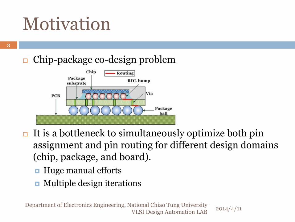
Motivation
2014/4/11 Department of Electronics Engineering, National Chiao Tung University
VLSI Design Automation LAB
3
Chip-package co-design problem
It is a bottleneck to simultaneously optimize both pin assignment and pin routing for different design domains (chip, package, and board).
Huge manual efforts
Multiple design iterations
Previous Works
2014/4/11 Department of Electronics Engineering, National Chiao Tung University
VLSI Design Automation LAB
4
Cross-domain co-design methodology
A board-driven Λ-shaped co-design flow [1]
A concurrent design flow [2]
[1] H. C. Lee and Y. W. Chang, “A chip-package-board co-design methodology,” in Proc. of ACM/IEEE Design Automation Conference, pp. 1082-1087, 2012.
[2] R. J. Lee and H. M. Chen, “A study of row-based area-array I/O design planning in concurrent chip-package design flow,” in Proc. of ACM Trans. on Design Automation of Electronic Systems, vol. 18, no. 2, pp. 1-19, 2013.
Our Contributions
2014/4/11 Department of Electronics Engineering, National Chiao Tung University
VLSI Design Automation LAB
5
A fast heuristic for chip-package co-design
A bump assignment which introduces high routability both in RDL routing and substrate routing (100% in our real case).
A practical RDL layout.
A routing order that guides designers to easily finish net connection on package.
A simulator: improper I/O-ball mapping can be fixed in the early stage.
Outline
2014/4/11 Department of Electronics Engineering, National Chiao Tung University
VLSI Design Automation LAB
6
Introduction
Preliminary
Pseudo single redistribution layer
Substrate routing
Problem formulation
Bump assignment and package planning
Experimental results
Conclusions
Pseudo Single RDL
2014/4/11 Department of Electronics Engineering, National Chiao Tung University
VLSI Design Automation LAB
7
a) Congested RDL
b) Extra routing area
c) Extra metal layer
d) Pseudo single-layer [3]
M9 is mainly for PG
Use less critical area
Avoid additional layers
Cost-effective
Existing style in manual routing
[3] H. W. Hsu, M. L. Chen, H. M. Chen, H. C. Li, and S. H. Chen, “On effective flip-chip routing via pseudo single redistribution layer,” in Proc. of Design, Automation and Test in Europe Conference and Exhibition, pp. 1597-1602, 2012.
Substrate Routing
2014/4/11 Department of Electronics Engineering, National Chiao Tung University
VLSI Design Automation LAB
8
Substrate routing is preferred to be planar, even though multiple routing layers are available [4].
The signal vias are allowed in very limited locations due to manufacturability, leaving space for P/G vias.
Vertical detour introduce extra vias, which may destroy the signal integrity for high-speed differential signals.
[4] S. Liu, G. Chen, T. T. Jing, L. He, T. Zhang, R. Dutta, and X. L. Hong, “Substrate topological routing for high-density packages,” in IEEE Trans. on Computer-Aided Design of Integrated Circuits and Systems, vol. 28, no. 2, pp. 207-216, Feb. 2009.
Outline
2014/4/11 Department of Electronics Engineering, National Chiao Tung University
VLSI Design Automation LAB
9
Introduction
Preliminary
Problem formulation
Bump assignment and package planning
Experimental results
Conclusions
Input
I/O pin sequence O.
Ball matrix B.
Output
Bump assignment U.
Physical RDL layout.
An illustration of planar substrate routing.
Objective
Chip: maximize routability in RDL routing and minimize routing area borrowed from another existing metal layer.
Package: maximize routability in substrate routing.
Problem Formulation
2014/4/11 Department of Electronics Engineering, National Chiao Tung University
VLSI Design Automation LAB
10
Outline
2014/4/11 Department of Electronics Engineering, National Chiao Tung University
VLSI Design Automation LAB
11
Introduction
Preliminary
Problem formulation
Bump assignment and package planning Design flow
Substrate routing
Bump assignment
RDL routing
Experimental results
Conclusions
Design Flow
Traditional flow costs more human resource and time because of the iteration.
We propose a straightforward co-design flow to automatically solve the problem in a short time.
2014/4/11
12
Department of Electronics Engineering, National Chiao Tung University VLSI Design Automation LAB
Outline
2014/4/11 Department of Electronics Engineering, National Chiao Tung University
VLSI Design Automation LAB
13
Introduction
Preliminary
Problem formulation
Bump assignment and package planning Design flow
Substrate routing B-Escape routing Net grouping
Bump assignment
RDL routing
Experimental results
Conclusions
B-Escape Routing Algorithm
2014/4/11 Department of Electronics Engineering, National Chiao Tung University
VLSI Design Automation LAB
14
A simultaneous escape is to find planar escape solutions in both components so that they are honoring the same escape ordering.
Two major techniques:
Boundary routing
Dynamic net ordering
[5] L. Luo, T. Yan, Q. Ma, M. D. F. Wong, and T. Shibuya, “B-escape: a simultaneous escape routing algorithm based on boundary routing,” in Proc. of International Symposium on Physical Design, pp. 19-25, 2010.
Detailed Structure
2014/4/11 Department of Electronics Engineering, National Chiao Tung University
VLSI Design Automation LAB
15
Four pin sequences specify the relations among I/O, bump, and ball: SO≃ SUc≃ SUp= SB
SO: I/O pin sequence.
SUc: a row-based projection of bump matrix on chip.
SUp: a row-based projection of bump matrix on package.
SB: the escape pin order of ball.
Net Grouping
2014/4/11 Department of Electronics Engineering, National Chiao Tung University
VLSI Design Automation LAB
16
We introduce I/O information into B-Escape routing algorithm by net grouping technique.
To simultaneously achieve high routability in both RDL routing and substrate routing.
Group nets based on:
I/O pin sequence
# bumps in a row
Cost: (α, β) → (α, β, γ)
α: trapped
β: blocked
γ is the group of net.
Cost Ordering
2014/4/11 Department of Electronics Engineering, National Chiao Tung University
VLSI Design Automation LAB
17
Inside group: non-decreasing order based on α and β.
Between groups: based on γ.
Upward mode: G1, G2, G3, …, Gn
Downward mode: Gn, …, G3, G2, G1
Backtrack and Reorder
2014/4/11 Department of Electronics Engineering, National Chiao Tung University
VLSI Design Automation LAB
18
While backtracking:
Ni and Nj are in the same group (higher priority)
Ni and Nj are in different groups
where Ni is the chosen net and Nj is the next candidate net
Reformation of B-Escape
2014/4/11 Department of Electronics Engineering, National Chiao Tung University
VLSI Design Automation LAB
19
□ Step1: calculate routing cost of each net
□ Step2: sort net costs
□ Step3: route the first net or backtrack
Between groups
Inside group
Outline
2014/4/11 Department of Electronics Engineering, National Chiao Tung University
VLSI Design Automation LAB
20
Introduction
Preliminary
Problem formulation
Bump assignment and package planning Design flow
Substrate routing
Bump assignment
RDL routing
Experimental results
Conclusions
Global Bump Assignment
2014/4/11 Department of Electronics Engineering, National Chiao Tung University
VLSI Design Automation LAB
21
Find bump assignment set according to the package escape routing result.
Detailed Bump Assignment
2014/4/11 Department of Electronics Engineering, National Chiao Tung University
VLSI Design Automation LAB
22
Choosing a solution from bump assignment set to make the difference between bump pin order and I/O pin order is minimum.
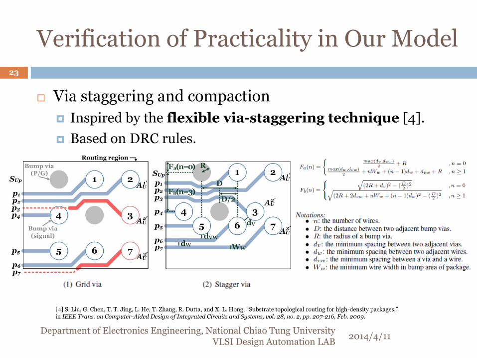
Verification of Practicality in Our Model
2014/4/11 Department of Electronics Engineering, National Chiao Tung University
VLSI Design Automation LAB
23
Via staggering and compaction
Inspired by the flexible via-staggering technique [4].
Based on DRC rules.
[4] S. Liu, G. Chen, T. T. Jing, L. He, T. Zhang, R. Dutta, and X. L. Hong, “Substrate topological routing for high-density packages,” in IEEE Trans. on Computer-Aided Design of Integrated Circuits and Systems, vol. 28, no. 2, pp. 207-216, Feb. 2009.
Outline
2014/4/11 Department of Electronics Engineering, National Chiao Tung University
VLSI Design Automation LAB
24
Introduction
Preliminary
Problem formulation
Bump assignment and package planning Design flow
Substrate routing
Bump assignment
RDL routing
Experimental results
Conclusions
Projection Method
2014/4/11 Department of Electronics Engineering, National Chiao Tung University
VLSI Design Automation LAB
25
Original projection method [3]
One direction
Cost more routing tracks
Reformation
Two directions
Reduce # routing tracks
[3] H. W. Hsu, M. L. Chen, H. M. Chen, H. C. Li, and S. H. Chen, “On effective flip-chip routing via pseudo single redistribution layer,” in Proc. of Design, Automation and Test in Europe Conference and Exhibition, pp. 1597-1602, 2012.
List of Bump Pin Track
2014/4/11 Department of Electronics Engineering, National Chiao Tung University
VLSI Design Automation LAB
26
RDL Routing
2014/4/11 Department of Electronics Engineering, National Chiao Tung University
VLSI Design Automation LAB
27
Step1: consider I/O pads as a pin track SO.
Step2: perform projection method on bump matrix to build a virtual pin track SUc.
Step3: channel routing on pseudo-single layer [3].
[3] H. W. Hsu, M. L. Chen, H. M. Chen, H. C. Li, and S. H. Chen, “On effective flip-chip routing via pseudo single redistribution layer,” in Proc. of Design, Automation and Test in Europe Conference and Exhibition, pp. 1597-1602, 2012.
Outline
2014/4/11 Department of Electronics Engineering, National Chiao Tung University
VLSI Design Automation LAB
28
Introduction
Preliminary
Problem formulation
Bump assignment and package planning
Experimental results
Conclusions
Experimental Results
2014/4/11 Department of Electronics Engineering, National Chiao Tung University
VLSI Design Automation LAB
29
Compared with traditional co-design flow, our work
costs less routing resource.
reduces design time.
saves manual effort. (automatically completes the whole process.)
Package Routability
2014/4/11 Department of Electronics Engineering, National Chiao Tung University
VLSI Design Automation LAB
30
Green path: the escape routing result.
Blue fly-line: bump-ball assignment.
RDL Routability
2014/4/11 Department of Electronics Engineering, National Chiao Tung University
VLSI Design Automation LAB
31
Based on our bump assignment, we can achieve 100% routability in RDL routing by [3].
[3] H. W. Hsu, M. L. Chen, H. M. Chen, H. C. Li, and S. H. Chen, “On effective flip-chip routing via pseudo single redistribution layer,” in Proc. of Design, Automation and Test in Europe Conference and Exhibition, pp. 1597-1602, 2012.
Outline
2014/4/11 Department of Electronics Engineering, National Chiao Tung University
VLSI Design Automation LAB
32
Introduction
Preliminary
Problem formulation
Bump assignment and package planning
Experimental results
Conclusions
Conclusions
2014/4/11 Department of Electronics Engineering, National Chiao Tung University
VLSI Design Automation LAB
33
We propose a straightforward chip-package co-design flow with routability-driven bump assignment based on:
Pseudo-single layer RDL routing [3].
B-Escape routing [5].
Net grouping offers information interactions between chip and package to avoid the iterative revise of bump assignment in traditional design flow.
Experimental results show that our work automatically completes the whole design process in a short time.
[3] H. W. Hsu, M. L. Chen, H. M. Chen, H. C. Li, and S. H. Chen, “On effective flip-chip routing via pseudo single redistribution layer,” in Proc. of Design, Automation and Test in Europe Conference and Exhibition, pp. 1597-1602, 2012. [5] L. Luo, T. Yan, Q. Ma, M. D. F. Wong, and T. Shibuya, “B-escape: a simultaneous escape routing algorithm based on boundary routing,” in Proc. of International Symposium on Physical Design, pp. 19-25, 2010.
References
2014/4/11 Department of Electronics Engineering, National Chiao Tung University
VLSI Design Automation LAB
34
[1] H. C. Lee and Y. W. Chang, “A chip-package-board co-design methodology,” in Proc. of ACM/IEEE Design Automation Conference, pp. 1082-1087, 2012.
[2] R. J. Lee and H. M. Chen, “A study of row-based area-array I/O design planning in concurrent chip-package design flow,” in Proc. of ACM Trans. on Design Automation of Electronic Systems, vol. 18, no. 2, pp. 1-19, 2013.
[3] H. W. Hsu, M. L. Chen, H. M. Chen, H. C. Li, and S. H. Chen, “On effective flip-chip routing via pseudo single redistribution layer,” in Proc. of Design, Automation and Test in Europe Conference and Exhibition, pp. 1597-1602, 2012.
[4] S. Liu, G. Chen, T. T. Jing, L. He, T. Zhang, R. Dutta, and X. L. Hong, “Substrate topological routing for high-density packages,” in IEEE Trans. on Computer-Aided Design of Integrated Circuits and Systems, vol. 28, no. 2, pp. 207-216, Feb. 2009.
[5] L. Luo, T. Yan, Q. Ma, M. D. F. Wong, and T. Shibuya, “B-escape: a simultaneous escape routing algorithm based on boundary routing,” in Proc. of International Symposium on Physical Design, pp. 19-25, 2010.