Wet thermal oxidation of GaAs and GaN 105 x Wet thermal oxidation of GaAs and GaN Ryszard Korbutowicz and Joanna Prażmowska Wroclaw University of Technology Poland 1. Introduction The chapter is devoted to the thermal wet oxidation of AIIIBV semiconductor compounds, mainly to gallium arsenide and gallium nitride. It has been divided into several topics, containing of monoclinic gallium oxide 1 -Ga 2 O 3 properties data, techniques of oxide fabrication and application description. In the first part, properties of mentioned semiconductor’s oxides are characterized. Then methods of manufacturing with a special attention for wet thermal oxidation are described. After that, applications of gallium oxide structures in electronics are given. It focuses also on the semiconductor structures dedicated for gas sensors application while gallium oxide layers improve significantly the most critical parameters of the detector compared to those containing of e.g. SnO 2 . AIIIBV and AIIIN semiconductors compounds are wide known as materials for optoelectronics devices. They are used often also to the construction of high temperature and microwave devices or chemical gas sensors. In these applications dielectric layers are necessary. There is a possibility of using their own oxides – Ga 2 O 3 gives a chance to manufacture many different devices – MOS structures (Metal-Oxide-Semiconductor). It can be MOS capacitors, power Metal Oxide Semiconductor Field Effect Transistors (MOSFETs), high mobility GaAs MOSFETs or gate turn-off thyristors and, probably, CMOS applications (Pearton et al., 1999; Wu et al., 2003). The MOS-gate version of the HEMT has significantly better thermal stability than a metal-gate structure and is well suited to gas sensing (Schweben et al., 1998; Baban et al., 2005; Hong et al., 2007). 2. Properties of -Ga 2 O 3 Gallium oxide -Ga 2 O 3 is a wide band gap material that ensures deep-UV transparency. Appropriately doped could reach conductive properties thus is included to the TCO’s (transparent conductive oxides) materials like ITO or ZnO which are the state-of-the-art materials in optoelectronics. Gallium oxide occurs in various structures like , , , , types (Kim & Kim, 2000). Among many polymorphs, monoclinic -Ga 2 O 3 is considered to be the equilibrium phase (Battiston et al., 1996; Chen et al., 2000; V´llora et al., 2004). It is stable thermally and chemically 1 The typical name for Ga2O3 are: digallium trioxide, gallium(III) oxide, gallium trioxide, gallium oxide. We use in the text term: gallium oxide. 6 www.intechopen.com
Transcript
Wet thermal oxidation of GaAs and GaN 105
Wet thermal oxidation of GaAs and GaN
Ryszard Korbutowicz and Joanna Prażmowska
x
Wet thermal oxidation of GaAs and GaN
Ryszard Korbutowicz and Joanna Prażmowska Wroclaw University of Technology
Poland
1 Introduction
The chapter is devoted to the thermal wet oxidation of AIIIBV semiconductor compounds mainly to gallium arsenide and gallium nitride It has been divided into several topics containing of monoclinic gallium oxide1 -Ga2O3 properties data techniques of oxide fabrication and application description In the first part properties of mentioned semiconductorrsquos oxides are characterized Then methods of manufacturing with a special attention for wet thermal oxidation are described After that applications of gallium oxide structures in electronics are given It focuses also on the semiconductor structures dedicated for gas sensors application while gallium oxide layers improve significantly the most critical parameters of the detector compared to those containing of eg SnO2 AIIIBV and AIIIN semiconductors compounds are wide known as materials for optoelectronics devices They are used often also to the construction of high temperature and microwave devices or chemical gas sensors In these applications dielectric layers are necessary There is a possibility of using their own oxides ndash Ga2O3 gives a chance to manufacture many different devices ndash MOS structures (Metal-Oxide-Semiconductor) It can be MOS capacitors power Metal Oxide Semiconductor Field Effect Transistors (MOSFETs) high mobility GaAs MOSFETs or gate turn-off thyristors and probably CMOS applications (Pearton et al 1999 Wu et al 2003) The MOS-gate version of the HEMT has significantly better thermal stability than a metal-gate structure and is well suited to gas sensing (Schweben et al 1998 Baban et al 2005 Hong et al 2007)
2 Properties of -Ga2O3
Gallium oxide -Ga2O3 is a wide band gap material that ensures deep-UV transparency Appropriately doped could reach conductive properties thus is included to the TCOrsquos (transparent conductive oxides) materials like ITO or ZnO which are the state-of-the-art materials in optoelectronics Gallium oxide occurs in various structures like types (Kim amp Kim 2000) Among many polymorphs monoclinic -Ga2O3 is considered to be the equilibrium phase (Battiston et al 1996 Chen et al 2000 Vacutellora et al 2004) It is stable thermally and chemically 1 The typical name for Ga2O3 are digallium trioxide gallium(III) oxide gallium trioxide gallium oxide We use in the text term gallium oxide
6
wwwintechopencom
Semiconductor Technologies106
(Battiston et al 1996 Vacutellora et al 2004) The thermal stability of -Ga2O3 reaches nearly melting point reported as 1740 C (Orita et al 2004) and 1807 C (Tomm et al 2000) or 2000 K (Vacutellora et al 2004) what determines also possibility of working at high temperature -Ga2O3 in monoclinic structure has a elemental unit dimensions as follows a=12214 Aring b=30371 Aring c=57981 Aring and =10383 (Tomm et al 2000) or a=1223 Aring b=304 Aring c=58 Aring and =1037 (Vacutellora et al 2004) Cleavage along (100) plane (Tomm et al 2000 Ueda a et al 1997 Vacutellora et al 2004) and (001) (Vacutellora et al 2004) are highly preferred The space group of -Ga2O3 is C2m (C32h) where GaO6 share octahedral sites along b and are connected by GaO4 tertrahedra thus anisotropy of optical as well as electrical properties is expected depending on the direction to the chains ndash perpendicular or parallel (Ueda b et al 1997) The -Ga2O3 unit cell along b c and a-axis could be found in (Vacutellora et al 2004)
21 Electrical properties At room temperature -Ga2O3 is an insulating material above 500 C has a semiconductor properties (Fleischer amp Meixner 1993 Battiston et al 1996 Frank et al 1996 Orita et al 2004) Although electrically conductive crystals of -Ga2O3 have been also reported see Table 1 (Vacutellora et al 2004)
direction resistivity mobility carrier concentration
cm cm2V-1s-1 cm-3
lt100gt 011 83 7x10¹⁷
lt010gt 019 78 4x10¹⁷ lt001gt 008 93 9x10¹⁷
Table 1 Electrical properties measured for β-Ga2O3 single crystal along certain direction
211 Electrical conductance The tetravalent tin ion Sn4+ is most often chosen as a donor dopant (Orita et al 2000 Orita et al 2004) because its ionic radius is close to that of Ga3+ and simultaneously Sn4+ ions prefer sixfold coordination This causes substituting of Ga3+ octahedral sites and results in formation of shallow donors (Orita et al 2004) Additionally formation of oxygen vacancies in the layer provides an occurrence of shallow levels as reported for -Ga2O3 crystals (Ueda a et al 1997) Thus much emphasize has been placed on the optimization of the deposition process conditions Alteration of ambient atmosphere and substrate temperature in eg PLD (Pulsed Lased Deposition) technology had significant impact on the properties of the layer In order to assure formation of oxygen vacancies and doping by Sn4+ low partial pressure of oxygen and elevation of substrate temperature to 880 C were applied It could increase chemical potential of oxygen in the lattice what introduces oxygen vacancies and solution of tin ions to the lattice Reported mobility of carriers was 044 cm2V-1s-1 and maximum electrical conductivity 10 Scm-1 These parameters were achieved for layers deposited on substrates maintained at 880 C under pressure equal to 6x10⁻⁵ Pa Increase of oxygen pressure to 13x10-2 Pa led to lowering of conductivity to 36x10-3 Scm-1 (Orita et al 2000) This effect was confirmed by Ueda et al (Ueda b et al 1997) for crystals obtained in floating zone technique increase of oxygen flow rate significantly affected electrical conductivity of investigated material (see Fig 1(a)) Under O2 atmosphere undoped crystals were insulating
lt10-9 -1cm-1 With addition of N2 to the atmosphere the conductivity increased and reached 063 -1cm-1 However the N2 content in the growth ambient is limited by the stability of crystals (Ueda a et al 1997) The maximum obtained electrical conductivity was 38 -1cm-1 for sample grown in gas mixture of N2O2 with partial pressure ratio of 0406 To achieve enhancement in conductivity of gallium oxide also Ti4+ and Zr4+ donor dopants in polycrystalline films for application in gas sensors were used (Frank et al 1996) Unexpected only slight increase in conductivity and decrease in sensitivity were obtained Thus SnO2 doping was applied by Frank et al The highest conductivity was reached for 05 SnO2 (see Fig 1 (b)) Doping possibility seems to be restricted due to solution in lattice limit (Frank b et al 1998)
(a)
005 010 015 020
1E-4
1E-3
001
01
1
Con
duct
ance
[S c
m-1]
O2 flow rate [m3h-1] (b)
08 09 10 11 1201
1
10
100
1000
Res
ista
nce
[kO
hm]
1000KT
undoped 01 Sn 05 Sn 3 Sn
Fig 1 (a) Electric conductivity of the β-Ga2O3 single crystals along the b-axis as a function of the O2 flow rate The closed circles - samples grown from undoped Ga2O3 rods open square - sample grown from Sn-doped Ga2O3 rods (Ueda a et al 1997) (b) Resistance in wet synthetic air of undoped and SnO2 doped thin films (Frank b et al 1998) Depending on orientation crystals grown in floating zone technique had resistivities as follows 011 lt100gt 019 lt010gt and 008 lt001gt cm (Vacutellora et al 2004) and those obtained by Ueda et al were 0026 cm (b-axis) and 045 cm (c-axis) (Ueda b et al 1997) Conductivity did not depend on temperature in the range of 0 ndash 300 K as shown in Fig 2
0 50 100 150 200 250 3001
10
100
a axis
c axis
Con
duct
ivity
[S c
m-1]
Temperature [K] Fig 2 Temperature dependence of the electrical conductivity along b- and a -axis of -Ga2O3 single crystals (Ueda b et al 1997) The Mg2+ was used as an acceptor dopant by Frank et al (Frank et al 1996) to achieve conversion to p-type semiconductive material from intrinsic n-type Layers sequence consisting of dopant and Ga2O3 was deposited on quartz glass substrates by reactive sputtering and subsequently annealed at temperatures up to 1200C Strong decrease of
wwwintechopencom
Wet thermal oxidation of GaAs and GaN 107
(Battiston et al 1996 Vacutellora et al 2004) The thermal stability of -Ga2O3 reaches nearly melting point reported as 1740 C (Orita et al 2004) and 1807 C (Tomm et al 2000) or 2000 K (Vacutellora et al 2004) what determines also possibility of working at high temperature -Ga2O3 in monoclinic structure has a elemental unit dimensions as follows a=12214 Aring b=30371 Aring c=57981 Aring and =10383 (Tomm et al 2000) or a=1223 Aring b=304 Aring c=58 Aring and =1037 (Vacutellora et al 2004) Cleavage along (100) plane (Tomm et al 2000 Ueda a et al 1997 Vacutellora et al 2004) and (001) (Vacutellora et al 2004) are highly preferred The space group of -Ga2O3 is C2m (C32h) where GaO6 share octahedral sites along b and are connected by GaO4 tertrahedra thus anisotropy of optical as well as electrical properties is expected depending on the direction to the chains ndash perpendicular or parallel (Ueda b et al 1997) The -Ga2O3 unit cell along b c and a-axis could be found in (Vacutellora et al 2004)
21 Electrical properties At room temperature -Ga2O3 is an insulating material above 500 C has a semiconductor properties (Fleischer amp Meixner 1993 Battiston et al 1996 Frank et al 1996 Orita et al 2004) Although electrically conductive crystals of -Ga2O3 have been also reported see Table 1 (Vacutellora et al 2004)
direction resistivity mobility carrier concentration
cm cm2V-1s-1 cm-3
lt100gt 011 83 7x10¹⁷
lt010gt 019 78 4x10¹⁷ lt001gt 008 93 9x10¹⁷
Table 1 Electrical properties measured for β-Ga2O3 single crystal along certain direction
211 Electrical conductance The tetravalent tin ion Sn4+ is most often chosen as a donor dopant (Orita et al 2000 Orita et al 2004) because its ionic radius is close to that of Ga3+ and simultaneously Sn4+ ions prefer sixfold coordination This causes substituting of Ga3+ octahedral sites and results in formation of shallow donors (Orita et al 2004) Additionally formation of oxygen vacancies in the layer provides an occurrence of shallow levels as reported for -Ga2O3 crystals (Ueda a et al 1997) Thus much emphasize has been placed on the optimization of the deposition process conditions Alteration of ambient atmosphere and substrate temperature in eg PLD (Pulsed Lased Deposition) technology had significant impact on the properties of the layer In order to assure formation of oxygen vacancies and doping by Sn4+ low partial pressure of oxygen and elevation of substrate temperature to 880 C were applied It could increase chemical potential of oxygen in the lattice what introduces oxygen vacancies and solution of tin ions to the lattice Reported mobility of carriers was 044 cm2V-1s-1 and maximum electrical conductivity 10 Scm-1 These parameters were achieved for layers deposited on substrates maintained at 880 C under pressure equal to 6x10⁻⁵ Pa Increase of oxygen pressure to 13x10-2 Pa led to lowering of conductivity to 36x10-3 Scm-1 (Orita et al 2000) This effect was confirmed by Ueda et al (Ueda b et al 1997) for crystals obtained in floating zone technique increase of oxygen flow rate significantly affected electrical conductivity of investigated material (see Fig 1(a)) Under O2 atmosphere undoped crystals were insulating
lt10-9 -1cm-1 With addition of N2 to the atmosphere the conductivity increased and reached 063 -1cm-1 However the N2 content in the growth ambient is limited by the stability of crystals (Ueda a et al 1997) The maximum obtained electrical conductivity was 38 -1cm-1 for sample grown in gas mixture of N2O2 with partial pressure ratio of 0406 To achieve enhancement in conductivity of gallium oxide also Ti4+ and Zr4+ donor dopants in polycrystalline films for application in gas sensors were used (Frank et al 1996) Unexpected only slight increase in conductivity and decrease in sensitivity were obtained Thus SnO2 doping was applied by Frank et al The highest conductivity was reached for 05 SnO2 (see Fig 1 (b)) Doping possibility seems to be restricted due to solution in lattice limit (Frank b et al 1998)
(a)
005 010 015 020
1E-4
1E-3
001
01
1
Con
duct
ance
[S c
m-1]
O2 flow rate [m3h-1] (b)
08 09 10 11 1201
1
10
100
1000
Res
ista
nce
[kO
hm]
1000KT
undoped 01 Sn 05 Sn 3 Sn
Fig 1 (a) Electric conductivity of the β-Ga2O3 single crystals along the b-axis as a function of the O2 flow rate The closed circles - samples grown from undoped Ga2O3 rods open square - sample grown from Sn-doped Ga2O3 rods (Ueda a et al 1997) (b) Resistance in wet synthetic air of undoped and SnO2 doped thin films (Frank b et al 1998) Depending on orientation crystals grown in floating zone technique had resistivities as follows 011 lt100gt 019 lt010gt and 008 lt001gt cm (Vacutellora et al 2004) and those obtained by Ueda et al were 0026 cm (b-axis) and 045 cm (c-axis) (Ueda b et al 1997) Conductivity did not depend on temperature in the range of 0 ndash 300 K as shown in Fig 2
0 50 100 150 200 250 3001
10
100
a axis
c axis
Con
duct
ivity
[S c
m-1]
Temperature [K] Fig 2 Temperature dependence of the electrical conductivity along b- and a -axis of -Ga2O3 single crystals (Ueda b et al 1997) The Mg2+ was used as an acceptor dopant by Frank et al (Frank et al 1996) to achieve conversion to p-type semiconductive material from intrinsic n-type Layers sequence consisting of dopant and Ga2O3 was deposited on quartz glass substrates by reactive sputtering and subsequently annealed at temperatures up to 1200C Strong decrease of
wwwintechopencom
Semiconductor Technologies108
conductivity was observed but values of this parameters were comparable for 03 and 3 of MgO what indicated on achievement of solubility limit already by 03 of MgO Bulk crystals of -Ga2O3 are electrically conductive but achievement of conductive layers has required many efforts Application of proper substrate is crucial The octahedral Ga3+ chains are responsible for generating paths for electrons thus growth of (-201) -Ga2O3 in which b axis is parallel to the substrates are considered as promising (Orita et al 2004) This requirement could be fulfilled by application of (0006) Al2O3 substrates
212 Carriers mobility Villora et al have measured carriers mobilities of three different oriented samples Results were 83 78 and 98 cm2V-1s-1 for lt100gt lt010gt and lt001gt directions respectively (Vacutellora et al 2004) Proper optimization of process in floating zone technology led to the achievement of carrier mobility of 46 cm2V-1s-1 for single crystals (Ueda b et al 1997) Electron mobility in single crystals and polycrystalline inhomogeneous porous ceramics of Ga2O3 was also investigated by M Fleischer et al at temperature from 800 C to 1000 C as in this range gas sensors operate (Fleischer amp Meixner 1993) Electron mobility determined from Hall measurement was nearly the same for both samples - 10 cm2V-1s-1 Also increase of mobility was observed with increasing the temperature of measurement Ueda et al (Ueda b et al 1997) have measured mobilities along b and c directions for floating zone obtained (100) platelets Mobility along b direction was of one order of magnitude larger than that for c direction Obtained values were as follows 46 cm2V-1s-1 (b-axis) and 26 cm2V-1s-1 (c-axis)
213 Dielectric constant and breakdown field Dielectric constant of gallium oxide is rather rarely investigated Value reported in (Zhou et al 2008) is of about 102 Shan et al (Shan et al 2005) have measured dielectric constant for thin layers deposited on p-Si (100) and sapphire (0001) substrates by PEALD (Plasma Enhanced Atomic Layer Deposition) Substrates temperature during the process was maintained at 200 C As-deposited layers were amorphous and had large leakage current Annealing at 700 or 900 C has improved that parameter but simultaneously layers dielectric constants decreased Figure 3 presents dielectric constants of as-deposited and annealed at various temperatures Ga2O3 thin films The breakdown fieldvoltage depends significantly on technology of fabrication of the material Values reported for thermally oxidized layers were 005-01 MVcm (Readinger et al 1999) 065 MVcm (Zhou et al 2008) 1 MVcm (Lin et al 2006) and 385 MVcm (Kim et al 2001) when those for PEALD were 1-15 MVcm (Shan et al 2005) and e-beam evaporation 36 MVcm (Passlack et al 1995)
200 400 600 800 1000
9
10
11
12
13
Die
lect
ric c
onst
ant
Temperature [oC] Fig 3 Dielectric constants of as-deposited Ga2O3 thin film and of those annealed at various RTA temperatures (Shan et al 2005)
22 Optical properties Gallium oxide is highly transparent in visible and near UV range of wavelengths (Vacutellora et al 2004) Transmittances in the range of visible light and UV range exceeding 80 were reported by (Matsuzuki et al 2006 Orita et al 2004 Ueda b et al 1997) and that reaching nearly 100 by (Shan et al 2005) Enhancement of transmittance could be obtained by increase of oxide layer deposition temperature (Orita et al 2004 Orita et al 2000) or appropriate annealing of crystals (Ueda a et al 1997) Because of the anisotropy of optical properties of -Ga2O3 the absorption edge depends on the angle of incident beam of light to the c or b direction of the crystal Assuming that is an angle between c-axis and electric field vector E Ueda et al have investigated the transmission of floating zone obtained (001) -Ga2O3 platelets with thickness of 0159 mm (Ueda 2 et al 1997) Figure 4 (a) presents the optical transmission spectra of an insulating -Ga2O3 for various The dichroism of the transmission spectra is remarkable It was also indentified by Tippins (Tippins 1965) and Ueda (Ueda a et al 1997) which observed absorption edge at 255 nm and additional shoulder at 275 nm The explanation of the dichroism could be found at (Ueda b et al 1997) Band gap energy Eg of gallium oxide varies in a wide range from 423 to 524 eV depending on the parameters of applied technology see Table 2 and Fig 4 (b) One of the parameters influencing the band gap is temperature of annealing of deposited layer Fig 4 (b)
(a)
250 260 270 280 2900
1020304050607080
90o
60o
45o
30o
=0o
Tran
smitt
ance
[]
Wavelength [nm] (b)
200 400 600 800 1000500
505
510
515
520
525
Ban
d ga
p en
ergy
[eV
]
Temperature [oC] Fig 4 (a) Optical transmission spectra of an insulating -Ga2O3 for various (Ueda b et al 1997) and (b) band gap energy of the as-deposited Ga2O3 and annealed at various temperatures thin films (Shan et al 2005)
wwwintechopencom
Wet thermal oxidation of GaAs and GaN 109
conductivity was observed but values of this parameters were comparable for 03 and 3 of MgO what indicated on achievement of solubility limit already by 03 of MgO Bulk crystals of -Ga2O3 are electrically conductive but achievement of conductive layers has required many efforts Application of proper substrate is crucial The octahedral Ga3+ chains are responsible for generating paths for electrons thus growth of (-201) -Ga2O3 in which b axis is parallel to the substrates are considered as promising (Orita et al 2004) This requirement could be fulfilled by application of (0006) Al2O3 substrates
212 Carriers mobility Villora et al have measured carriers mobilities of three different oriented samples Results were 83 78 and 98 cm2V-1s-1 for lt100gt lt010gt and lt001gt directions respectively (Vacutellora et al 2004) Proper optimization of process in floating zone technology led to the achievement of carrier mobility of 46 cm2V-1s-1 for single crystals (Ueda b et al 1997) Electron mobility in single crystals and polycrystalline inhomogeneous porous ceramics of Ga2O3 was also investigated by M Fleischer et al at temperature from 800 C to 1000 C as in this range gas sensors operate (Fleischer amp Meixner 1993) Electron mobility determined from Hall measurement was nearly the same for both samples - 10 cm2V-1s-1 Also increase of mobility was observed with increasing the temperature of measurement Ueda et al (Ueda b et al 1997) have measured mobilities along b and c directions for floating zone obtained (100) platelets Mobility along b direction was of one order of magnitude larger than that for c direction Obtained values were as follows 46 cm2V-1s-1 (b-axis) and 26 cm2V-1s-1 (c-axis)
213 Dielectric constant and breakdown field Dielectric constant of gallium oxide is rather rarely investigated Value reported in (Zhou et al 2008) is of about 102 Shan et al (Shan et al 2005) have measured dielectric constant for thin layers deposited on p-Si (100) and sapphire (0001) substrates by PEALD (Plasma Enhanced Atomic Layer Deposition) Substrates temperature during the process was maintained at 200 C As-deposited layers were amorphous and had large leakage current Annealing at 700 or 900 C has improved that parameter but simultaneously layers dielectric constants decreased Figure 3 presents dielectric constants of as-deposited and annealed at various temperatures Ga2O3 thin films The breakdown fieldvoltage depends significantly on technology of fabrication of the material Values reported for thermally oxidized layers were 005-01 MVcm (Readinger et al 1999) 065 MVcm (Zhou et al 2008) 1 MVcm (Lin et al 2006) and 385 MVcm (Kim et al 2001) when those for PEALD were 1-15 MVcm (Shan et al 2005) and e-beam evaporation 36 MVcm (Passlack et al 1995)
200 400 600 800 1000
9
10
11
12
13
Die
lect
ric c
onst
ant
Temperature [oC] Fig 3 Dielectric constants of as-deposited Ga2O3 thin film and of those annealed at various RTA temperatures (Shan et al 2005)
22 Optical properties Gallium oxide is highly transparent in visible and near UV range of wavelengths (Vacutellora et al 2004) Transmittances in the range of visible light and UV range exceeding 80 were reported by (Matsuzuki et al 2006 Orita et al 2004 Ueda b et al 1997) and that reaching nearly 100 by (Shan et al 2005) Enhancement of transmittance could be obtained by increase of oxide layer deposition temperature (Orita et al 2004 Orita et al 2000) or appropriate annealing of crystals (Ueda a et al 1997) Because of the anisotropy of optical properties of -Ga2O3 the absorption edge depends on the angle of incident beam of light to the c or b direction of the crystal Assuming that is an angle between c-axis and electric field vector E Ueda et al have investigated the transmission of floating zone obtained (001) -Ga2O3 platelets with thickness of 0159 mm (Ueda 2 et al 1997) Figure 4 (a) presents the optical transmission spectra of an insulating -Ga2O3 for various The dichroism of the transmission spectra is remarkable It was also indentified by Tippins (Tippins 1965) and Ueda (Ueda a et al 1997) which observed absorption edge at 255 nm and additional shoulder at 275 nm The explanation of the dichroism could be found at (Ueda b et al 1997) Band gap energy Eg of gallium oxide varies in a wide range from 423 to 524 eV depending on the parameters of applied technology see Table 2 and Fig 4 (b) One of the parameters influencing the band gap is temperature of annealing of deposited layer Fig 4 (b)
(a)
250 260 270 280 2900
1020304050607080
90o
60o
45o
30o
=0o
Tran
smitt
ance
[]
Wavelength [nm] (b)
200 400 600 800 1000500
505
510
515
520
525
Ban
d ga
p en
ergy
[eV
]
Temperature [oC] Fig 4 (a) Optical transmission spectra of an insulating -Ga2O3 for various (Ueda b et al 1997) and (b) band gap energy of the as-deposited Ga2O3 and annealed at various temperatures thin films (Shan et al 2005)
wwwintechopencom
Semiconductor Technologies110
Refractive indexes of gallium oxide are generally in the range of 18-19 Ueda et al have reported in (Ueda a et al 1997) for single crystals values of 184 and 188 at 980 nm those for e-beam evaporated layers were 1841-1885 at 980 nm (Passlack et al 1995) for PEALD 189 (Shan et al 2005) and for bulk 191 (Passlack et al 1995)
500 Al2O3 (0001) plasma enhanced ALD (Shan et al 2005) 49 α-Al2O3
silica PLD (Matsuzuki et al 2006)
(Orita et al 2000) 484 fused silica e-beam evaporation with no excess of oxygen (Al-Kuhaili et al 2003) 479 - floating zone (along b-axis) (Ueda b et al 1997) 475 quartz spray pyrolysis (Hao amp Cocivera 2002) 474 Si (001) rf magnetron sputtering (Rebien et al 2002) 472
GaAs e-beam evaporation (Rebien et al 2002)
46 - Czochralski (Tomm et al 2000) 452 - floating zone (along c-axis) (Ueda b et al 1997) 448 quartz spray pyrolysis (annealed at 600 ordmC) (Hao amp Cocivera 2002) 444 quartz spray pyrolysis (annealed at 900 ordmC) (Hao amp Cocivera 2002) 423 borosilicate
glass spray pyrolysis (Kim amp Kim 2000)
Table 2 Bang gap energy values of gallium oxide for various techniques
23 Crystalline quality and morphology Depending on deposition technology gallium oxide layers are generally amorphous as reported for samples obtained by PEALD (Shan et al 2005) MOVPE (Metalorganic Vapor Phase Epitaxy) (Battiston et al 1996 Kim amp Kim 2004) or PLD (Orita et al 2004) Crystallization of films could be assured by its annealing at high temperature (Battiston et al 1996 Kim amp Kim 2004 Shan et al 2005) increase of substrates temperature (Orita et al 2004) or oxidation at high temperatures For example amorphous layers of -Ga2O3 deposited on (0001) Al2O3 substrates in PLD at 325 C were obtained by Orita et al Diffraction peaks appeared in layers deposited at temperatures above 380 C (Orita et al 2004) In case of CVD (Chemical Vapor Deposition) -Ga2O3 layers annealing process at temperatures above 700 C assured crystallization Crystalline properties of gallium oxide are usually determined based on XRD (X-Ray Diffraction) with CuK radiation measurement of 2 patterns The most commonly appearing peaks are (-202) (400) and (-111) at 2 angle of about 100deg 54deg and 17deg (Battiston et al 1996) or (11-3) and (30-6) at 39 and 59 (Chen et al 2000) as well as (-206) and (-306) at 496 and 591 (Kim et al 2001) Except of crystallites directions determination XRD method is applied to the estimation of crystallites sizes For this purpose broadening of peak widths is investigated and Sherrer formula applied Crystallites sizes are usually in the range from 20 to 50 nm (Battiston et al 1996 Frank et al 1996) and could be enlarged by temperature of annealing increase The root mean square of layers varies in the range from 5 to 25 Aring Reported values were as follows 5 Aring (Shan et al 2005) 8-13 Aring (Wolter et al 2000) 10-20 Aring (Matsuzaki et al 2006) and 12-23 Aring (Kim amp Kim 2004)
There is a variety of other parameters of oxides apart from those described and analyzed above Authors refer to photoluminescence studies to (Hao amp Cocivera 2002) density of interface states (Lin et al 2005 Lin et al 2006 Nakano b et al 2003 Zhou et al 2008) or oxidation states as well as etching behavior (Passlack et al 1995)
3 Fabrication of the gallium oxide layers
There are several methods of manufacturing of gallium oxide for semiconductor devices applications One can after CW Wilmsen (Wilmsen 1985) say that the main ways are (a) chemical oxidation (b) thermal oxidation (c) anodic oxidation (d) plasma oxidation and (e) other methods Dry or wet thermal oxidation are also applied Since several years bulk crystals of Ga2O3 are available (Tomm et al 2000 Vacutellora et al 2004) as well Thermal oxidation of AIIIBV and AIIIN compounds ndash dry (Wilmsen 1985 Lin et al 2000) or wet (Readinger et al 1999) ndash is unfortunately not similar to silicon oxidation It is caused by other structure ndash these compounds consist of two or more elements which variously react with oxygen and water In addition AIIIBVs and AIIINs are very thermodynamically unstable ndash especially As and N have high partial pressures In spite of these difficulties in many laboratories one carry on thermal oxidation studies because this technique is relatively cheap and can give good results The most known is AlAs oxidation for diode lasers (especially VCSEL lasers) electroluminescent diodes and detectors with Bragg reflectors (Geib et al 1997 Pucicki et al 2004)
31 Chemical oxidation Typical chemical oxidizers for GaAs are HNO3 with H2O2 and H2O Chemical oxidation method is used as a part of surface GaAs substrates cleaning and rather is not used for making gallium oxide layers for devices (Ghidaoui 2002)
32 Electrochemical (anodic) oxidation Oxidation of semiconductors electrochemical anodic process is similar to typical process of oxide layer manufacturing in electrolyte Anodic process is more efficient if in semiconductor materials holes occur ndash type p of electrical conduction For type n it is necessary to generate holes in order to facilitate oxidation The easier way is illumination by the appropriate light ndash with photon energy in the range from 14 eV to 5 eV (Wilmsen 1985) The level of the photon energies depends on energy bandgap of the semiconductor The process is simple in the theory Problems appear with increasing of the oxide thickness ndash both electrical resistivity of oxide layer and diffusion rate of the oxidizing factor in the layer are variable Problem that could appear is a choice of the appropriate electrolyte ndash it depends on the material anodic equipment etc One should to make electrical contacts to the semiconductor permanent or temporary which have to be stable in the applied electrolyte Oxides after anodic process of GaAs are a mixture of gallium and arsenic oxides These layers are not tight and ought to be annealed in high temperature (more than 450 degC) At this temperature arsenic oxides dissociate and gallium oxide will remain crystalline The anodic oxidation of n-type GaN (17 microm thick layer on sapphire substrate with carrier concentration of 46 times 1018 cmndash3) under laboratory illumination at a constant current density of 5 mAcmndash2 in sodium tungstate electrolyte (01 MNa2WO42H2O) at 298 K was made by
wwwintechopencom
Wet thermal oxidation of GaAs and GaN 111
Refractive indexes of gallium oxide are generally in the range of 18-19 Ueda et al have reported in (Ueda a et al 1997) for single crystals values of 184 and 188 at 980 nm those for e-beam evaporated layers were 1841-1885 at 980 nm (Passlack et al 1995) for PEALD 189 (Shan et al 2005) and for bulk 191 (Passlack et al 1995)
500 Al2O3 (0001) plasma enhanced ALD (Shan et al 2005) 49 α-Al2O3
silica PLD (Matsuzuki et al 2006)
(Orita et al 2000) 484 fused silica e-beam evaporation with no excess of oxygen (Al-Kuhaili et al 2003) 479 - floating zone (along b-axis) (Ueda b et al 1997) 475 quartz spray pyrolysis (Hao amp Cocivera 2002) 474 Si (001) rf magnetron sputtering (Rebien et al 2002) 472
GaAs e-beam evaporation (Rebien et al 2002)
46 - Czochralski (Tomm et al 2000) 452 - floating zone (along c-axis) (Ueda b et al 1997) 448 quartz spray pyrolysis (annealed at 600 ordmC) (Hao amp Cocivera 2002) 444 quartz spray pyrolysis (annealed at 900 ordmC) (Hao amp Cocivera 2002) 423 borosilicate
glass spray pyrolysis (Kim amp Kim 2000)
Table 2 Bang gap energy values of gallium oxide for various techniques
23 Crystalline quality and morphology Depending on deposition technology gallium oxide layers are generally amorphous as reported for samples obtained by PEALD (Shan et al 2005) MOVPE (Metalorganic Vapor Phase Epitaxy) (Battiston et al 1996 Kim amp Kim 2004) or PLD (Orita et al 2004) Crystallization of films could be assured by its annealing at high temperature (Battiston et al 1996 Kim amp Kim 2004 Shan et al 2005) increase of substrates temperature (Orita et al 2004) or oxidation at high temperatures For example amorphous layers of -Ga2O3 deposited on (0001) Al2O3 substrates in PLD at 325 C were obtained by Orita et al Diffraction peaks appeared in layers deposited at temperatures above 380 C (Orita et al 2004) In case of CVD (Chemical Vapor Deposition) -Ga2O3 layers annealing process at temperatures above 700 C assured crystallization Crystalline properties of gallium oxide are usually determined based on XRD (X-Ray Diffraction) with CuK radiation measurement of 2 patterns The most commonly appearing peaks are (-202) (400) and (-111) at 2 angle of about 100deg 54deg and 17deg (Battiston et al 1996) or (11-3) and (30-6) at 39 and 59 (Chen et al 2000) as well as (-206) and (-306) at 496 and 591 (Kim et al 2001) Except of crystallites directions determination XRD method is applied to the estimation of crystallites sizes For this purpose broadening of peak widths is investigated and Sherrer formula applied Crystallites sizes are usually in the range from 20 to 50 nm (Battiston et al 1996 Frank et al 1996) and could be enlarged by temperature of annealing increase The root mean square of layers varies in the range from 5 to 25 Aring Reported values were as follows 5 Aring (Shan et al 2005) 8-13 Aring (Wolter et al 2000) 10-20 Aring (Matsuzaki et al 2006) and 12-23 Aring (Kim amp Kim 2004)
There is a variety of other parameters of oxides apart from those described and analyzed above Authors refer to photoluminescence studies to (Hao amp Cocivera 2002) density of interface states (Lin et al 2005 Lin et al 2006 Nakano b et al 2003 Zhou et al 2008) or oxidation states as well as etching behavior (Passlack et al 1995)
3 Fabrication of the gallium oxide layers
There are several methods of manufacturing of gallium oxide for semiconductor devices applications One can after CW Wilmsen (Wilmsen 1985) say that the main ways are (a) chemical oxidation (b) thermal oxidation (c) anodic oxidation (d) plasma oxidation and (e) other methods Dry or wet thermal oxidation are also applied Since several years bulk crystals of Ga2O3 are available (Tomm et al 2000 Vacutellora et al 2004) as well Thermal oxidation of AIIIBV and AIIIN compounds ndash dry (Wilmsen 1985 Lin et al 2000) or wet (Readinger et al 1999) ndash is unfortunately not similar to silicon oxidation It is caused by other structure ndash these compounds consist of two or more elements which variously react with oxygen and water In addition AIIIBVs and AIIINs are very thermodynamically unstable ndash especially As and N have high partial pressures In spite of these difficulties in many laboratories one carry on thermal oxidation studies because this technique is relatively cheap and can give good results The most known is AlAs oxidation for diode lasers (especially VCSEL lasers) electroluminescent diodes and detectors with Bragg reflectors (Geib et al 1997 Pucicki et al 2004)
31 Chemical oxidation Typical chemical oxidizers for GaAs are HNO3 with H2O2 and H2O Chemical oxidation method is used as a part of surface GaAs substrates cleaning and rather is not used for making gallium oxide layers for devices (Ghidaoui 2002)
32 Electrochemical (anodic) oxidation Oxidation of semiconductors electrochemical anodic process is similar to typical process of oxide layer manufacturing in electrolyte Anodic process is more efficient if in semiconductor materials holes occur ndash type p of electrical conduction For type n it is necessary to generate holes in order to facilitate oxidation The easier way is illumination by the appropriate light ndash with photon energy in the range from 14 eV to 5 eV (Wilmsen 1985) The level of the photon energies depends on energy bandgap of the semiconductor The process is simple in the theory Problems appear with increasing of the oxide thickness ndash both electrical resistivity of oxide layer and diffusion rate of the oxidizing factor in the layer are variable Problem that could appear is a choice of the appropriate electrolyte ndash it depends on the material anodic equipment etc One should to make electrical contacts to the semiconductor permanent or temporary which have to be stable in the applied electrolyte Oxides after anodic process of GaAs are a mixture of gallium and arsenic oxides These layers are not tight and ought to be annealed in high temperature (more than 450 degC) At this temperature arsenic oxides dissociate and gallium oxide will remain crystalline The anodic oxidation of n-type GaN (17 microm thick layer on sapphire substrate with carrier concentration of 46 times 1018 cmndash3) under laboratory illumination at a constant current density of 5 mAcmndash2 in sodium tungstate electrolyte (01 MNa2WO42H2O) at 298 K was made by
wwwintechopencom
Semiconductor Technologies112
Pakes et al (Pakes et al 2003) They have observed local oxidation and that the oxidation has occurred at troughs in the faceted GaN layers Near the peaks in the faceted surface oxidation was negligible The localized nature of the oxidation of the GaN is presumed after authors to be related to the strength of the Ga-N bond and non-uniform distributions of impurity non-stoichiometry or defects in the substrate (Pakes et al 2003) The oxide was non-uniform and textured with pore-like features The absence of a compact anodic film is probably due to extensive generation of nitrogen during anodic oxidation which disrupts development of a uniform anodic film Peng et al (Peng et al 2001) have patented the method of nitride material oxidation enhanced by illumination with UV light at room temperature Authors used 254-nm UV light to illuminate the GaN crystals to generate electron-hole pairs The pH value of the electrolyte was in the range of approximately 3 to 10 preferably about 35 The authors (Peng et al 2001) claim that ldquoThis invention allows the rapid formation of gallium oxide at room temperature and it is possible to monitor the thickness of the oxide in-situ by means of measuring the loop currentrdquo
33 Plasma oxidation By plasma oxidation of GaAs gaseous plasma containing oxygen are used The sources of oxygen are O2 N2O or CO2 and it is excited by a RF coil (Wilmsen 1985 Hartnagel amp Riemenschnieder 1999) A DC bias oxidation takes place in a similar way to the wet anodization process In the oxide layers without thermal treatment Ga2O3 and As2O3 almost in equal proportions were found Ions which attacked substrate can sputter the surface and thus lead to a reduced growth rate and to a modification of surface stoichiometry due to a preferential sputtering of the arsenic component (Hartnagel amp Riemenschnieder 1999) The plasma parameters (RF frequency RF power and gas pressure) may not affect the oxide growth but they do affect the degree of GaAs surface degradation during the initial stage of oxide formation In contrast wet anodic oxidations give almost damage-free oxides
34 Dry thermal oxidation Dry thermal oxidation processes of GaAs and GaN are carried out in ambient of oxygen or mixture of nitrogen and oxygen Dry oxidation of GaAs is made rather seldom Processes are very complicated because of problems with arsenic and its low thermal stability Typical top oxide layers on GaAs surface consist of mixture Ga2O3 + GaAsO4 + As2O3 and are rough Near the interface of oxide-gallium arsenide occur Ga2O3 and elemental As (after Wilmsen 1985) These layers are amorphous By higher oxidation temperature (above 500 degC) oxides are polycrystalline and also rather rough They contain mainly Ga2O3 but GaAsO4 was also observed The elemental As small crystallites of As2O5 and As2O3 appeared in layers as well (after Pessegi et al 1998) Arsenic oxides have low thermal stability and during annealing processes oxides undergo decomposition releasing arsenic which escapes from the samples Thermal oxidation of GaAs technique has more than thirty years Thermal oxidation of GaN epilayers is a considerably younger ndash it is a matter of last ten years Gallium nitride needs higher temperature as GaAs or AlAs typical range of dry oxidation is between 800 and 1100 degC (Chen et al 2000) Processes are carried out usually in atmosphere of oxygen (Chen et al 2000 Lin et al 2006) Chen at al (Chen et al 2000) described several
experiments with GaN layers on sapphire substrates Authors made oxidation of GaN samples in dry oxygen Time of oxidation was changed from 20 min to 8 h by the flow of O2 of about 1 slm Temperature was changed from 800 to 1100 degC They have observed two different courses for temperatures of over 1000 degC very rapid oxidation process in the initial stage of oxidation and then after about 1 h followed by a relatively slow process Authors have deliberated after Wolter et al (Wolter et al 1998) the reaction rate constant and have concluded that in the first step of oxidation (rapid process) the oxide creation reaction is limited by the rate of reaction on GaN-oxide interface In second step (slow process by thicker oxide layers) the oxide creation reaction is determined by the diffusion-controlled mechanism (transition from reaction-controlled mechanism to the diffusion-controlled mechanism) They have supposed GaN decomposition at high temperature (over 1000 degC) which can speed up the gallium oxidation (Chen et al 2000) The authors also have observed volume increase of about 40 after oxidation Similar experiments were made by Zhou et al (Zhou et al 2008) by oxidation of GaN powder and GaN free-standing substrates with Ga-terminated surface (front side) from HVPE epitaxial processes They have used dry oxygen as a reactor chamber atmosphere only and have changed time (from 4 to 12 hours) and temperature (850 900 950 and 950 degC) of oxidation According to authors oxidation rate in temperature below 750 degC is negligible They have made similar analysis as Chen et al (Chen et al 2000) after Wolter et al (Wolter et al 1998) and observed similar dependence of the oxide thickness versus time process In GaN dry oxidation processes one could observe two zones interfacial reaction-controlled and diffusion-controlled mechanism for low and high temperature respectively (Zhou et al 2008) Authors of this paper have wrote about ldquothermally grown gallium oxide on () GaN substraterdquo It is typical for many authors although all of them described oxidation process
35 Wet thermal oxidation Problems in wet thermal oxidation of GaAs processes are very similar to those which occur during dry oxidation Arsenic in GaAs has low thermal stability in high temperature and it is rather difficult to carry out oxidation process at the temperature higher than 600 degC The applied temperatures from the range below 600 degC gave not rewarding results The obtained by Korbutowicz et al (Korbutowicz et al 2008) gallium oxide layers have been very thin and had have weak adhesion Processes of wet thermal GaN oxidation are carried out more often Gallium nitride has better thermal stability than gallium arsenide and one can apply higher temperature to obtained Ga2O3 is thicker and has better parameters Typical apparatus for wet thermal oxidation of GaAs or GaN is very similar to that which is applied to wet thermal oxidation of AlAs or AlxGa1-xAs It can be Closed Chamber System CCS (a) or Open Chamber System OCS (b) The open systems are more often used as the systems with closed tube one
351 Close chamber systems Choe et al have described in their paper (Choe et al 2000) CCS equipment for AlAs oxidation which was schematically depicted in Figure 5 a It also can be applied to GaAs oxidation The quartz reaction (oxidation) chamber had two temperature zones ndash the upper and lower zone one for the sample and second for the water source It was small chamber ndash
wwwintechopencom
Wet thermal oxidation of GaAs and GaN 113
Pakes et al (Pakes et al 2003) They have observed local oxidation and that the oxidation has occurred at troughs in the faceted GaN layers Near the peaks in the faceted surface oxidation was negligible The localized nature of the oxidation of the GaN is presumed after authors to be related to the strength of the Ga-N bond and non-uniform distributions of impurity non-stoichiometry or defects in the substrate (Pakes et al 2003) The oxide was non-uniform and textured with pore-like features The absence of a compact anodic film is probably due to extensive generation of nitrogen during anodic oxidation which disrupts development of a uniform anodic film Peng et al (Peng et al 2001) have patented the method of nitride material oxidation enhanced by illumination with UV light at room temperature Authors used 254-nm UV light to illuminate the GaN crystals to generate electron-hole pairs The pH value of the electrolyte was in the range of approximately 3 to 10 preferably about 35 The authors (Peng et al 2001) claim that ldquoThis invention allows the rapid formation of gallium oxide at room temperature and it is possible to monitor the thickness of the oxide in-situ by means of measuring the loop currentrdquo
33 Plasma oxidation By plasma oxidation of GaAs gaseous plasma containing oxygen are used The sources of oxygen are O2 N2O or CO2 and it is excited by a RF coil (Wilmsen 1985 Hartnagel amp Riemenschnieder 1999) A DC bias oxidation takes place in a similar way to the wet anodization process In the oxide layers without thermal treatment Ga2O3 and As2O3 almost in equal proportions were found Ions which attacked substrate can sputter the surface and thus lead to a reduced growth rate and to a modification of surface stoichiometry due to a preferential sputtering of the arsenic component (Hartnagel amp Riemenschnieder 1999) The plasma parameters (RF frequency RF power and gas pressure) may not affect the oxide growth but they do affect the degree of GaAs surface degradation during the initial stage of oxide formation In contrast wet anodic oxidations give almost damage-free oxides
34 Dry thermal oxidation Dry thermal oxidation processes of GaAs and GaN are carried out in ambient of oxygen or mixture of nitrogen and oxygen Dry oxidation of GaAs is made rather seldom Processes are very complicated because of problems with arsenic and its low thermal stability Typical top oxide layers on GaAs surface consist of mixture Ga2O3 + GaAsO4 + As2O3 and are rough Near the interface of oxide-gallium arsenide occur Ga2O3 and elemental As (after Wilmsen 1985) These layers are amorphous By higher oxidation temperature (above 500 degC) oxides are polycrystalline and also rather rough They contain mainly Ga2O3 but GaAsO4 was also observed The elemental As small crystallites of As2O5 and As2O3 appeared in layers as well (after Pessegi et al 1998) Arsenic oxides have low thermal stability and during annealing processes oxides undergo decomposition releasing arsenic which escapes from the samples Thermal oxidation of GaAs technique has more than thirty years Thermal oxidation of GaN epilayers is a considerably younger ndash it is a matter of last ten years Gallium nitride needs higher temperature as GaAs or AlAs typical range of dry oxidation is between 800 and 1100 degC (Chen et al 2000) Processes are carried out usually in atmosphere of oxygen (Chen et al 2000 Lin et al 2006) Chen at al (Chen et al 2000) described several
experiments with GaN layers on sapphire substrates Authors made oxidation of GaN samples in dry oxygen Time of oxidation was changed from 20 min to 8 h by the flow of O2 of about 1 slm Temperature was changed from 800 to 1100 degC They have observed two different courses for temperatures of over 1000 degC very rapid oxidation process in the initial stage of oxidation and then after about 1 h followed by a relatively slow process Authors have deliberated after Wolter et al (Wolter et al 1998) the reaction rate constant and have concluded that in the first step of oxidation (rapid process) the oxide creation reaction is limited by the rate of reaction on GaN-oxide interface In second step (slow process by thicker oxide layers) the oxide creation reaction is determined by the diffusion-controlled mechanism (transition from reaction-controlled mechanism to the diffusion-controlled mechanism) They have supposed GaN decomposition at high temperature (over 1000 degC) which can speed up the gallium oxidation (Chen et al 2000) The authors also have observed volume increase of about 40 after oxidation Similar experiments were made by Zhou et al (Zhou et al 2008) by oxidation of GaN powder and GaN free-standing substrates with Ga-terminated surface (front side) from HVPE epitaxial processes They have used dry oxygen as a reactor chamber atmosphere only and have changed time (from 4 to 12 hours) and temperature (850 900 950 and 950 degC) of oxidation According to authors oxidation rate in temperature below 750 degC is negligible They have made similar analysis as Chen et al (Chen et al 2000) after Wolter et al (Wolter et al 1998) and observed similar dependence of the oxide thickness versus time process In GaN dry oxidation processes one could observe two zones interfacial reaction-controlled and diffusion-controlled mechanism for low and high temperature respectively (Zhou et al 2008) Authors of this paper have wrote about ldquothermally grown gallium oxide on () GaN substraterdquo It is typical for many authors although all of them described oxidation process
35 Wet thermal oxidation Problems in wet thermal oxidation of GaAs processes are very similar to those which occur during dry oxidation Arsenic in GaAs has low thermal stability in high temperature and it is rather difficult to carry out oxidation process at the temperature higher than 600 degC The applied temperatures from the range below 600 degC gave not rewarding results The obtained by Korbutowicz et al (Korbutowicz et al 2008) gallium oxide layers have been very thin and had have weak adhesion Processes of wet thermal GaN oxidation are carried out more often Gallium nitride has better thermal stability than gallium arsenide and one can apply higher temperature to obtained Ga2O3 is thicker and has better parameters Typical apparatus for wet thermal oxidation of GaAs or GaN is very similar to that which is applied to wet thermal oxidation of AlAs or AlxGa1-xAs It can be Closed Chamber System CCS (a) or Open Chamber System OCS (b) The open systems are more often used as the systems with closed tube one
351 Close chamber systems Choe et al have described in their paper (Choe et al 2000) CCS equipment for AlAs oxidation which was schematically depicted in Figure 5 a It also can be applied to GaAs oxidation The quartz reaction (oxidation) chamber had two temperature zones ndash the upper and lower zone one for the sample and second for the water source It was small chamber ndash
wwwintechopencom
Semiconductor Technologies114
3 cm in diameter by 30 cm in length Typical amount of water was about 2 cm3 Chamber with sample and water was closed and the air was evacuated using a pump After this hermetically closed chamber was inserted into a furnace During the heating water was expanded as a vapour and filled whole volume of the quartz ampoule Typical temperature in the upper zone was 410 degC and in the lower zone was varied from 80 degC to 220 degC In this apparatus the oxidation process is controlled by two parameters temperature of oxidation and temperature of water source These systems have some advantages reaction kinetics in controlled by two temperatures oxidation and water vapour creation there is a small demand of oxidizing agent ndash water and no carrier gas A considerable inconvenience is the necessity of vacuum pumps application
352 Open chamber systems Open chamber system for GaAs and GaN oxidation looks like silicon oxidation system It consists of horizontal (very often) quartz tube water bubbler and source of the gases carrier ndash nitrogen N2 or argon Ar and (sometimes) oxygen O2 (Choquette et al 1997 Readinger et al 1999 Pucicki et al 2004 Geib et al 2007 Korbutowicz et al 2008) The three-zone resistant furnace works as a system heating (Fig 5 b) Korbutowicz et al (Korbutowicz et al 2008) have used the bubbler (in the heating jacket with a temperature control) with deionized water H2O as a source of oxidizing agent and nitrogen N2 as a main gas and the initial water level was the same in all experiments to keep the same conditions of the carrier gas saturation
(a) (b)
N2
3-zone furnace
heater with temperature control
bubbler with DI water
thermocouplerotameters
reactor chamber
Fig 5 (a) A schematic diagram of the CCS for wet thermal oxidation (Choe et al 2000) (b) typical apparatus for GaAs and GaN wet thermal oxidation The open systems are cheaper as the closed ones The work with the OCSrsquos are more complicated ndash one need to take into consideration numerous parameters source water temperature reaction temperature main gas flow and flow of the carrier gas through the bubbler kind of gases and using or not of oxygen The significant water consumption during oxidation and the requirement of the water source temperature stabilization also constitute problems But the valuable advantage of open systems is their simple construction Thermal wet oxidation method as a more frequently applied way to get gallium oxide layers will be wider described now Reaction kinetics of thermal wet oxidation and reaction results depend on several parameters a zone reaction temperature (a) a water source temperature (water bubbler) (b)
a flow of a main currier gas (c) a flow of a carrier gas through the water bubbler (d) time of the reaction (e) and type of currier gas (f) Korbutowicz et al (Korbutowicz et al 2008) have described processes of the GaAs and GaN thermal wet oxidation ndash GaAs wafers and GaN layers manufactured by MOVPE and HVPE (Hydride Vapor Phase Epitaxy) on sapphire substrates were used in these studies GaAs in form of bare wafers (one side polished Te doped) or wafers with epilayers (Si doped) were employed in investigations A range of oxidation temperature was between 483 and 526 degC Time was varied from 60 to 300 minutes Typical main flow of nitrogen was 2 800 sccmmin and typical flows through the water bubbler were 260 and 370 sccmmin Thicknesses of the gallium oxides layers grown on gallium arsenide substrates surface were uneven ndash it was visible to the naked eye one can observed variable colors on the surface (see Fig 6 (a)) Defects are preferable points to create oxide ndash from these spots started the oxidation process (Fig 6 (b)) Authors were able to obtain thin layers only since by longer process duration oxide layers were cracked and exfoliated In Fig 6 (c) one can see that oxide layers were thin and transparent Occurring cracks show that in interface region of GaAs-oxide exists a considerable strain
(a) (b) (c)
Fig 6 Views of oxide surfacersquos layers from optical microscope variable colors of gallium oxide (a) substratersquos defect and oxide (b) cracked and exfoliated oxide layer (c) Two kinds of GaN samples have been used ndash GaN epilayers deposited on sapphire substrates ndash thin layers from MOVPE and thick layers from HVPE with surface as grown Temperature of oxidation was higher as for GaAs samples and was as follows 755 795 and 827 degC Typical water temperature was 95 or 96 degC The main flows of nitrogen were varied from 1 450 to 2 800 sccmmin and the flows through the water bubbler were altered from 260 to 430 sccmmin The total gas flow in the reactor chamber was about 3 000 sccmmin In order to determine suitable parameters temperature of water source and temperature of reaction (oxidation) zone were changed Gas flows and time of the process were varied also The obtained thicknesses of gallium oxide were from several nanometers up to hundreds of nanometers The MOVPE GaN layers has much more smoother surface as from HVPE ones The influence of this difference one can remark after oxidation Optical observations by using naked eyes and optical microscope gave a lot of information about morphology of surface with oxide One can observe (Fig 7) eg smoothing of GaN hexagonal islands Wet oxidation of gallium arsenide appeared to be more difficult than that of GaN The Ga2O3 layers which were obtained by Korbutowicz et al were heterogeneous (see below results from X-ray diffraction ndash Fig 8)
wwwintechopencom
Wet thermal oxidation of GaAs and GaN 115
3 cm in diameter by 30 cm in length Typical amount of water was about 2 cm3 Chamber with sample and water was closed and the air was evacuated using a pump After this hermetically closed chamber was inserted into a furnace During the heating water was expanded as a vapour and filled whole volume of the quartz ampoule Typical temperature in the upper zone was 410 degC and in the lower zone was varied from 80 degC to 220 degC In this apparatus the oxidation process is controlled by two parameters temperature of oxidation and temperature of water source These systems have some advantages reaction kinetics in controlled by two temperatures oxidation and water vapour creation there is a small demand of oxidizing agent ndash water and no carrier gas A considerable inconvenience is the necessity of vacuum pumps application
352 Open chamber systems Open chamber system for GaAs and GaN oxidation looks like silicon oxidation system It consists of horizontal (very often) quartz tube water bubbler and source of the gases carrier ndash nitrogen N2 or argon Ar and (sometimes) oxygen O2 (Choquette et al 1997 Readinger et al 1999 Pucicki et al 2004 Geib et al 2007 Korbutowicz et al 2008) The three-zone resistant furnace works as a system heating (Fig 5 b) Korbutowicz et al (Korbutowicz et al 2008) have used the bubbler (in the heating jacket with a temperature control) with deionized water H2O as a source of oxidizing agent and nitrogen N2 as a main gas and the initial water level was the same in all experiments to keep the same conditions of the carrier gas saturation
(a) (b)
N2
3-zone furnace
heater with temperature control
bubbler with DI water
thermocouplerotameters
reactor chamber
Fig 5 (a) A schematic diagram of the CCS for wet thermal oxidation (Choe et al 2000) (b) typical apparatus for GaAs and GaN wet thermal oxidation The open systems are cheaper as the closed ones The work with the OCSrsquos are more complicated ndash one need to take into consideration numerous parameters source water temperature reaction temperature main gas flow and flow of the carrier gas through the bubbler kind of gases and using or not of oxygen The significant water consumption during oxidation and the requirement of the water source temperature stabilization also constitute problems But the valuable advantage of open systems is their simple construction Thermal wet oxidation method as a more frequently applied way to get gallium oxide layers will be wider described now Reaction kinetics of thermal wet oxidation and reaction results depend on several parameters a zone reaction temperature (a) a water source temperature (water bubbler) (b)
a flow of a main currier gas (c) a flow of a carrier gas through the water bubbler (d) time of the reaction (e) and type of currier gas (f) Korbutowicz et al (Korbutowicz et al 2008) have described processes of the GaAs and GaN thermal wet oxidation ndash GaAs wafers and GaN layers manufactured by MOVPE and HVPE (Hydride Vapor Phase Epitaxy) on sapphire substrates were used in these studies GaAs in form of bare wafers (one side polished Te doped) or wafers with epilayers (Si doped) were employed in investigations A range of oxidation temperature was between 483 and 526 degC Time was varied from 60 to 300 minutes Typical main flow of nitrogen was 2 800 sccmmin and typical flows through the water bubbler were 260 and 370 sccmmin Thicknesses of the gallium oxides layers grown on gallium arsenide substrates surface were uneven ndash it was visible to the naked eye one can observed variable colors on the surface (see Fig 6 (a)) Defects are preferable points to create oxide ndash from these spots started the oxidation process (Fig 6 (b)) Authors were able to obtain thin layers only since by longer process duration oxide layers were cracked and exfoliated In Fig 6 (c) one can see that oxide layers were thin and transparent Occurring cracks show that in interface region of GaAs-oxide exists a considerable strain
(a) (b) (c)
Fig 6 Views of oxide surfacersquos layers from optical microscope variable colors of gallium oxide (a) substratersquos defect and oxide (b) cracked and exfoliated oxide layer (c) Two kinds of GaN samples have been used ndash GaN epilayers deposited on sapphire substrates ndash thin layers from MOVPE and thick layers from HVPE with surface as grown Temperature of oxidation was higher as for GaAs samples and was as follows 755 795 and 827 degC Typical water temperature was 95 or 96 degC The main flows of nitrogen were varied from 1 450 to 2 800 sccmmin and the flows through the water bubbler were altered from 260 to 430 sccmmin The total gas flow in the reactor chamber was about 3 000 sccmmin In order to determine suitable parameters temperature of water source and temperature of reaction (oxidation) zone were changed Gas flows and time of the process were varied also The obtained thicknesses of gallium oxide were from several nanometers up to hundreds of nanometers The MOVPE GaN layers has much more smoother surface as from HVPE ones The influence of this difference one can remark after oxidation Optical observations by using naked eyes and optical microscope gave a lot of information about morphology of surface with oxide One can observe (Fig 7) eg smoothing of GaN hexagonal islands Wet oxidation of gallium arsenide appeared to be more difficult than that of GaN The Ga2O3 layers which were obtained by Korbutowicz et al were heterogeneous (see below results from X-ray diffraction ndash Fig 8)
wwwintechopencom
Semiconductor Technologies116
Fig 7 HVPE GaN layer surface after wet thermal oxidation Figure 8 shows x-ray spectrum of gallium compounds on sapphire substrate (G32 sample) One can remark that oxidized surface layer contained GaN Ga2O3 and GaxNOy
Fig 8 X-ray diffraction spectrum of oxidized GaN on sapphire from HVPE G32_SMT2 ndash spectrum from thick GaN layer The MOVPE GaN crystals had smoother surface as HVPE crystals and were more resistant for oxidation In Figure 9 results of AFM (Atomic Force Microscope) observations of the surface and profile of MOVPE sample thickness of 880 (nm) (a) and HVPE sample thickness of 12 (microm) (b) are shown Both samples were oxidized in the same conditions reaction temperature of 827 degC water source temperature of 95 degC process time of 120 min and the same water vapour concentration The initial surface of MOVPE sample was smooth while the surface of HVPE thick layers was rather rough The oxidation process was faster by HVPE crystals because at these crystals surfaces was more developed The surface of oxidized GaN from MOVPE remained smooth whereas on the surface of the sample from HVPE one could observe typical little bumps
(a)
(b)
Fig 9 AFM images of the surface of GaN(MOVPE) sample (a) and GaN(HVPE) sample (b) Readinger et al (Readinger et al 1999) have carried out processes applying GaN powder and GaN thick layers on sapphire from vertical HVPE Atomic percentage of water vapor in carrier gas (O2 N2 and Ar) was maintained on the same level (778) for all furnace temperatures (700 750 800 850 and 900 degC) and carrier gas combinations For comparison purposes authors have prepared a dry oxidation processes (in dry oxygen) for the same samples Samplersquos surfaces after wet oxidation were much smoother as from dry process The authors have observed that below 700 degC in which GaN has a good stability in oxidizing environments They also have found that in ambient of oxygen (dry or wet) the oxidation had faster rate as in wet nitrogen or argon atmosphere Thicknesses of gallium oxide layers in wet O2 process revealed linear dependence on duration of oxidation Wet oxidation have given even poorer electrical results than dry oxidation The authors have judged that electrical parameters deterioration aroused from very irregular morphology at the wet oxideGaN interface
36 Other oxidation methods These above mentioned oxidation methods are not the only ways to get gallium oxide There are several others ones ion-beam induced oxidation (after Hartnagel amp Riemenschnieder 1999) laser assisted oxidation (Bermudez 1983) low-temperature oxidation (after Hartnagel amp Riemenschnieder 1999) photowash oxidation (Offsay et al 1986) oxidation by an atomic oxygen beam (after Hartnagel amp Riemenschnieder 1999) UVozone oxidation (after Hartnagel amp Riemenschnieder 1999) vacuum ultraviolet photochemical oxidation (Yu et al 1988)
37 Summary Apart from above mentioned methods are several other ways to obtain or manufacture gallium oxide layers One can deposited by Chemical Vapour Deposition CVD Physical Vapour Deposition PVD or Physical Vapour Transport PVT methods One can use Local Anodic Oxidation LAO by applying AFM equipment (Matsuzaki et al 2000 Lazzarino et al 2005 Lazzarino et al 2006) to GaAs or GaN surface oxidizing and creating small regions
wwwintechopencom
Wet thermal oxidation of GaAs and GaN 117
Fig 7 HVPE GaN layer surface after wet thermal oxidation Figure 8 shows x-ray spectrum of gallium compounds on sapphire substrate (G32 sample) One can remark that oxidized surface layer contained GaN Ga2O3 and GaxNOy
Fig 8 X-ray diffraction spectrum of oxidized GaN on sapphire from HVPE G32_SMT2 ndash spectrum from thick GaN layer The MOVPE GaN crystals had smoother surface as HVPE crystals and were more resistant for oxidation In Figure 9 results of AFM (Atomic Force Microscope) observations of the surface and profile of MOVPE sample thickness of 880 (nm) (a) and HVPE sample thickness of 12 (microm) (b) are shown Both samples were oxidized in the same conditions reaction temperature of 827 degC water source temperature of 95 degC process time of 120 min and the same water vapour concentration The initial surface of MOVPE sample was smooth while the surface of HVPE thick layers was rather rough The oxidation process was faster by HVPE crystals because at these crystals surfaces was more developed The surface of oxidized GaN from MOVPE remained smooth whereas on the surface of the sample from HVPE one could observe typical little bumps
(a)
(b)
Fig 9 AFM images of the surface of GaN(MOVPE) sample (a) and GaN(HVPE) sample (b) Readinger et al (Readinger et al 1999) have carried out processes applying GaN powder and GaN thick layers on sapphire from vertical HVPE Atomic percentage of water vapor in carrier gas (O2 N2 and Ar) was maintained on the same level (778) for all furnace temperatures (700 750 800 850 and 900 degC) and carrier gas combinations For comparison purposes authors have prepared a dry oxidation processes (in dry oxygen) for the same samples Samplersquos surfaces after wet oxidation were much smoother as from dry process The authors have observed that below 700 degC in which GaN has a good stability in oxidizing environments They also have found that in ambient of oxygen (dry or wet) the oxidation had faster rate as in wet nitrogen or argon atmosphere Thicknesses of gallium oxide layers in wet O2 process revealed linear dependence on duration of oxidation Wet oxidation have given even poorer electrical results than dry oxidation The authors have judged that electrical parameters deterioration aroused from very irregular morphology at the wet oxideGaN interface
36 Other oxidation methods These above mentioned oxidation methods are not the only ways to get gallium oxide There are several others ones ion-beam induced oxidation (after Hartnagel amp Riemenschnieder 1999) laser assisted oxidation (Bermudez 1983) low-temperature oxidation (after Hartnagel amp Riemenschnieder 1999) photowash oxidation (Offsay et al 1986) oxidation by an atomic oxygen beam (after Hartnagel amp Riemenschnieder 1999) UVozone oxidation (after Hartnagel amp Riemenschnieder 1999) vacuum ultraviolet photochemical oxidation (Yu et al 1988)
37 Summary Apart from above mentioned methods are several other ways to obtain or manufacture gallium oxide layers One can deposited by Chemical Vapour Deposition CVD Physical Vapour Deposition PVD or Physical Vapour Transport PVT methods One can use Local Anodic Oxidation LAO by applying AFM equipment (Matsuzaki et al 2000 Lazzarino et al 2005 Lazzarino et al 2006) to GaAs or GaN surface oxidizing and creating small regions
wwwintechopencom
Semiconductor Technologies118
covered by gallium oxide As was told earlier in chapter 2 the best parameters for semiconductor devices has monoclinic -Ga2O3 This type of oxide is easy to obtain by thermal oxidation dry or wet These methods also give possibility to selective oxidation using dielectric mask (eg SiO2) Despite the difficulties and problems on account of numerous process parameters which ought to be taken into consideration wet thermal oxidation of GaAs and GaN processes seem to be the best way for making oxide layers for devices applications
4 Applications of gallium oxide structures in electronics
Due to existent of native silicon oxide domination of silicon in electronics lasts many years Semiconductor compounds as AIIIBV or AIIIN have very good parameters which just predestine to work in a region of high frequencies and a high temperature with a high power insulating substrates high carrier mobility and wide bandgap These all give a big advantage over Si and their alloys But silicon still dominates Why SiO2 is an amorphous material which does not bring strain in underlying silicon Gallium arsenide GaAs applied in semiconductor devices technology has cubic crystal structure (as other AIIIBV compounds) and typical surface orientation (100) Gallium oxide with monoclinic structure which is the only variety of Ga2O3 stable in high temperature that stays stable after cooling is strongly mismatched to GaAs It causes bad relationships between GaAs epitaxial layers and oxide In addition gallium oxide growth on a surface of gallium arsenide is in a reality a mixture of Ga2O3 As2O3 As2O5 and elemental As as was mentioned above This mixture is unstable at elevated temperature and has poor dielectric parameters In order to avoid problems with the growth of Ga2O3 on GaAs surface some of researches have applied thin dielectric layer of Al2O3 in GaAs MOSFET structure (eg Jun 2000) but it is not a matter of our consideration By GaN oxidation is other situation than by GaAs treatment Gallium nitride applied in electronics has hexagonal structure and is better matched GaN in comparison to GaAs is more chemical thermal and environmental resistant Therefore nitrides are more often used to construction of numerous devices with a oxide-semiconductor structure MOS diodes and transistors gas and chemical sensors Silicon electronics supremacy was a result of among others applying of silicon oxide SiO2 possibility Properties of interface silicon oxide and silicon are just excellent This fact allows manufacturing of very-large scale integration circuits with Complementary Metal Oxide Semiconductor (CMOS) transistors (Hong 2008) But silicon devices encounter difficulties going to nanoscale ndash very thin dielectric gate layers is too thin and there is no effect charge carriers can flow through the gate dielectric by the quantum mechanical tunnelling mechanism Leakage current is too high ndash Si devices need dielectrics with higher electrical permittivity k Also power devices made from silicon and their alloys operate in smaller range of power and frequency One can draw a conclusion MOS devices need high k gate dielectric and carriers with higher mobility in channels of transistors as in siliconrsquos ones Whole microelectronics requires something else for example indium phosphide diamond silicon carbide gallium arsenide or gallium nitride and their alloys (see Fig 10 (Kasu 2004))
Fig 10 Demand for high-frequency high-power semiconductors to support the rise in communication capacity (Kasu 2004) Despite very good properties AIIIBV and AIIIN have problems to become commonly used especially in power applications A big obstacle is a lack of high quality stable gate dielectrics with high value of dielectric constant In opinion Ye (Ye 2008) ldquoThe physics and chemistry of IIIndashV compound semiconductor surfaces or interfaces are problems so complex that our understanding is still limited even after enormous research effortsrdquo and that can be the purpose although first GaAs MOSFETs was reported by Becke and White in 1965 (after Ye 2008) still there are problems with wide scale production One can deposit silicon dioxide silicon nitride and similar dielectrics but these materials have relatively small dielectric constant SiO2 has dielectric constant equal to 39 Si3N4 has constant = 75 but silicon nitride is not easy in a treatment Typical value of dielectric constant given in literature for Ga2O3 is in a range from 99 to 142 (Passlack et al 1995 Pearton et al 1999)
41 Metal Oxide Semiconductor devices The first thermal-oxide gate GaAs MOSFET was reported in the work of Takagi et al in 1978 (Takagi et al 1978) The gate oxide which has been grown by the new GaAs oxidation technique in the As2O3 vapor was chemically stable Oxidation process was carried out in a closed quartz ampoule Temperature of liquid arsenic trioxide was equal to 470 degC and temperature of GaAs (gallium oxide growth) was 500 degC Authors supposed that this method can be used in large scale as a fabrication process But up to now it is not the typical manufacture technique Typical GaAs MOSFET has the gate dielectric in the form of oxides mixture Ga2O3(Gd2O3) This mixture comes not from oxidation but from UHV deposition (eg Passlack et al 1997 Hong et al 2007 Passlack et al 2007) Practically almost all papers of Passlackrsquos team from the last twenty years have described oxide structures this type Ga2O3(Gd2O3) which were made in UHV apparatus Difficulties with obtaining good Ga2O3 layers on GaAs from thermal oxidation inclined researches to make GaAs MOS structures with oxidized thin layer of AlGaAs or InAlP but then aluminium is oxidized not gallium (eg Jing et al 2008) Matter of the GaN MOS structures looks similar and different too In many cases gate dielectric is Gadolinium Gallium Garnet (GGG) Gd3Ga5O12 called also Gadolinium Gallium
wwwintechopencom
Wet thermal oxidation of GaAs and GaN 119
covered by gallium oxide As was told earlier in chapter 2 the best parameters for semiconductor devices has monoclinic -Ga2O3 This type of oxide is easy to obtain by thermal oxidation dry or wet These methods also give possibility to selective oxidation using dielectric mask (eg SiO2) Despite the difficulties and problems on account of numerous process parameters which ought to be taken into consideration wet thermal oxidation of GaAs and GaN processes seem to be the best way for making oxide layers for devices applications
4 Applications of gallium oxide structures in electronics
Due to existent of native silicon oxide domination of silicon in electronics lasts many years Semiconductor compounds as AIIIBV or AIIIN have very good parameters which just predestine to work in a region of high frequencies and a high temperature with a high power insulating substrates high carrier mobility and wide bandgap These all give a big advantage over Si and their alloys But silicon still dominates Why SiO2 is an amorphous material which does not bring strain in underlying silicon Gallium arsenide GaAs applied in semiconductor devices technology has cubic crystal structure (as other AIIIBV compounds) and typical surface orientation (100) Gallium oxide with monoclinic structure which is the only variety of Ga2O3 stable in high temperature that stays stable after cooling is strongly mismatched to GaAs It causes bad relationships between GaAs epitaxial layers and oxide In addition gallium oxide growth on a surface of gallium arsenide is in a reality a mixture of Ga2O3 As2O3 As2O5 and elemental As as was mentioned above This mixture is unstable at elevated temperature and has poor dielectric parameters In order to avoid problems with the growth of Ga2O3 on GaAs surface some of researches have applied thin dielectric layer of Al2O3 in GaAs MOSFET structure (eg Jun 2000) but it is not a matter of our consideration By GaN oxidation is other situation than by GaAs treatment Gallium nitride applied in electronics has hexagonal structure and is better matched GaN in comparison to GaAs is more chemical thermal and environmental resistant Therefore nitrides are more often used to construction of numerous devices with a oxide-semiconductor structure MOS diodes and transistors gas and chemical sensors Silicon electronics supremacy was a result of among others applying of silicon oxide SiO2 possibility Properties of interface silicon oxide and silicon are just excellent This fact allows manufacturing of very-large scale integration circuits with Complementary Metal Oxide Semiconductor (CMOS) transistors (Hong 2008) But silicon devices encounter difficulties going to nanoscale ndash very thin dielectric gate layers is too thin and there is no effect charge carriers can flow through the gate dielectric by the quantum mechanical tunnelling mechanism Leakage current is too high ndash Si devices need dielectrics with higher electrical permittivity k Also power devices made from silicon and their alloys operate in smaller range of power and frequency One can draw a conclusion MOS devices need high k gate dielectric and carriers with higher mobility in channels of transistors as in siliconrsquos ones Whole microelectronics requires something else for example indium phosphide diamond silicon carbide gallium arsenide or gallium nitride and their alloys (see Fig 10 (Kasu 2004))
Fig 10 Demand for high-frequency high-power semiconductors to support the rise in communication capacity (Kasu 2004) Despite very good properties AIIIBV and AIIIN have problems to become commonly used especially in power applications A big obstacle is a lack of high quality stable gate dielectrics with high value of dielectric constant In opinion Ye (Ye 2008) ldquoThe physics and chemistry of IIIndashV compound semiconductor surfaces or interfaces are problems so complex that our understanding is still limited even after enormous research effortsrdquo and that can be the purpose although first GaAs MOSFETs was reported by Becke and White in 1965 (after Ye 2008) still there are problems with wide scale production One can deposit silicon dioxide silicon nitride and similar dielectrics but these materials have relatively small dielectric constant SiO2 has dielectric constant equal to 39 Si3N4 has constant = 75 but silicon nitride is not easy in a treatment Typical value of dielectric constant given in literature for Ga2O3 is in a range from 99 to 142 (Passlack et al 1995 Pearton et al 1999)
41 Metal Oxide Semiconductor devices The first thermal-oxide gate GaAs MOSFET was reported in the work of Takagi et al in 1978 (Takagi et al 1978) The gate oxide which has been grown by the new GaAs oxidation technique in the As2O3 vapor was chemically stable Oxidation process was carried out in a closed quartz ampoule Temperature of liquid arsenic trioxide was equal to 470 degC and temperature of GaAs (gallium oxide growth) was 500 degC Authors supposed that this method can be used in large scale as a fabrication process But up to now it is not the typical manufacture technique Typical GaAs MOSFET has the gate dielectric in the form of oxides mixture Ga2O3(Gd2O3) This mixture comes not from oxidation but from UHV deposition (eg Passlack et al 1997 Hong et al 2007 Passlack et al 2007) Practically almost all papers of Passlackrsquos team from the last twenty years have described oxide structures this type Ga2O3(Gd2O3) which were made in UHV apparatus Difficulties with obtaining good Ga2O3 layers on GaAs from thermal oxidation inclined researches to make GaAs MOS structures with oxidized thin layer of AlGaAs or InAlP but then aluminium is oxidized not gallium (eg Jing et al 2008) Matter of the GaN MOS structures looks similar and different too In many cases gate dielectric is Gadolinium Gallium Garnet (GGG) Gd3Ga5O12 called also Gadolinium Gallium
wwwintechopencom
Semiconductor Technologies120
Oxide (GGO) a synthetic crystalline material of the garnet group or Ga2O3(Gd2O3) (eg Gila et al 2000) as by GaAs MOSFETs Some researches tried to make Ga2O3 layer on GaN as dielectric film for MOS applications MOS capacitors (Kim et al 2001 Nakano amp Jimbo 2003) or MOS diodes (Nakano a et al 2003) Kim et al (Kim et al 2001) were studied dry thermal oxidation of GaN in ambient of oxygen It was a furnace oxidation at 850 degC for 12 h which resulted in the formation of monoclinic -Ga2O3 layer 88 nm in thickness Authors have analyzed the structural properties of the oxidized sample by SEM (scanning electron microscopy) XRD and AES (Auger Electron Spectroscopy) measurements In order to develop the electrical characteristics of the thermally oxidized GaN film a MOS capacitor was fabricated Based on observations and measurements authors have found that (i) the formation of monoclinic -Ga2O3 occurred (ii) the breakdown field strength of the thermal oxide was 385 MVcm-1 and (iii) the CndashV curves showed a low oxide charge density (Nf) of 6771011 cm-2 After Kim et al it suggests that the thermally grown Ga2O3 is promising for GaN-based power MOSFET applications (Kim et al 2001) Nakano amp Jimbo (Nakano amp Jimbo 2003) have described their study on the interface properties of thermally oxidized n type GaN metalndashoxidendashsemiconductor capacitors fabricated on sapphire substrates A 100 nm thick -Ga2O3 was grown by dry oxidation at 880 degC for 5 h After epitaxial growth authors have made typical lateral dot-and-ring -Ga2O3GaN MOS capacitors by a thermal oxidation method In order to reach this aim a 500 nm thick Si layer was deposited on the top surface of the GaN sample as a mask material for thermal oxidation Formation of monoclinic -Ga2O3 was confirmed by XRD They have also observed from SIMS (secondary ion mass spectrometry) measurements an intermediate Ga oxynitride layer with graded compositions at the -Ga2O3GaN interface (see Fig 11) The presence of GaNO was remarked by Korbutowicz et al (Korbutowicz et al 2008) in samples from the wet thermal oxidation after XRD measurements as well Nakano amp Jimbo (Nakano amp Jimbo 2003) have not observed in the Cndash t and DLTS (Deep Level Transient Spectroscopy) measurements discrete interface traps They have judged that it is in reasonable agreement with the deep depletion feature and low interface state density of 5531010 eV-1cm-2 revealed by the CndashV measurements They have supposed that the surface Fermi level can probably be unpinned at the -Ga2O3GaN MOS structures fabricated by a thermal oxidation technique The authors have compared as well the sputtered SiO2GaN MOS and -Ga2O3GaN MOS samples in DLTS measurements In Fig 12 results of this study were shown In contrast to the -Ga2O3GaN MOS structure SiO2GaN MOS sample has a large number of interface traps may induce the surface Fermi-level pinning at the MOS interface resulting in the capacitance saturation observed in the deep depletion region of the CndashV curve (Nakano amp Jimbo 2003) In slightly later publication of Nakano et al (Nakano a et al 2003) have described electrical properties of thermally oxidized p-GaN MOS diodes with n+ source regions fabricated on Al2O3 substrates Oxide was grown in the same way as in paper (Nakano amp Jimbo 2003) Results obtained by authors in this study have suggested that the thermally grown -Ga2O3p-GaN MOS structure is a promising candidate for inversion-mode MOSFET
Fig 11 SIMS profiles of Ga N and O atoms in the thermally oxidized -Ga2O3GaN MOS structure (Nakano amp Jimbo 2003)
Fig 12 Typical DLTS spectra at a rate window t1t2 of 10 ms20 ms for the thermally oxidized -Ga2O3GaN MOS and sputtered SiO2n-GaN MOS structures after applying the bias voltage of 225 V (Nakano amp Jimbo 2003) Lin et al (Lin et al 2006) have studied the influence of oxidation and annealing temperature on quality of Ga2O3 grown on GaN GaN wafers were oxidized at 750 degC 800 degC and 850 degC Authors have measured the electrical characteristics and interface quality of the resulting MOS capacitors have compared The process steps for making GaN MOS capacitor is shown in Fig 13 The 300-nm SiO2 layer was deposited on the GaN surface by radio-frequency sputtering to play as a mask for oxidation
(1) (2) (3) (4) (5) (6)
Fig 13 Process flow for GaN MOS capacitor (Lin et al 2006) Oxidation was carried out in dry oxygen ambient and followed by a 05 h annealing in argon at the same temperature as oxidation GaN oxidized at a higher temperature of 850 degC
wwwintechopencom
Wet thermal oxidation of GaAs and GaN 121
Oxide (GGO) a synthetic crystalline material of the garnet group or Ga2O3(Gd2O3) (eg Gila et al 2000) as by GaAs MOSFETs Some researches tried to make Ga2O3 layer on GaN as dielectric film for MOS applications MOS capacitors (Kim et al 2001 Nakano amp Jimbo 2003) or MOS diodes (Nakano a et al 2003) Kim et al (Kim et al 2001) were studied dry thermal oxidation of GaN in ambient of oxygen It was a furnace oxidation at 850 degC for 12 h which resulted in the formation of monoclinic -Ga2O3 layer 88 nm in thickness Authors have analyzed the structural properties of the oxidized sample by SEM (scanning electron microscopy) XRD and AES (Auger Electron Spectroscopy) measurements In order to develop the electrical characteristics of the thermally oxidized GaN film a MOS capacitor was fabricated Based on observations and measurements authors have found that (i) the formation of monoclinic -Ga2O3 occurred (ii) the breakdown field strength of the thermal oxide was 385 MVcm-1 and (iii) the CndashV curves showed a low oxide charge density (Nf) of 6771011 cm-2 After Kim et al it suggests that the thermally grown Ga2O3 is promising for GaN-based power MOSFET applications (Kim et al 2001) Nakano amp Jimbo (Nakano amp Jimbo 2003) have described their study on the interface properties of thermally oxidized n type GaN metalndashoxidendashsemiconductor capacitors fabricated on sapphire substrates A 100 nm thick -Ga2O3 was grown by dry oxidation at 880 degC for 5 h After epitaxial growth authors have made typical lateral dot-and-ring -Ga2O3GaN MOS capacitors by a thermal oxidation method In order to reach this aim a 500 nm thick Si layer was deposited on the top surface of the GaN sample as a mask material for thermal oxidation Formation of monoclinic -Ga2O3 was confirmed by XRD They have also observed from SIMS (secondary ion mass spectrometry) measurements an intermediate Ga oxynitride layer with graded compositions at the -Ga2O3GaN interface (see Fig 11) The presence of GaNO was remarked by Korbutowicz et al (Korbutowicz et al 2008) in samples from the wet thermal oxidation after XRD measurements as well Nakano amp Jimbo (Nakano amp Jimbo 2003) have not observed in the Cndash t and DLTS (Deep Level Transient Spectroscopy) measurements discrete interface traps They have judged that it is in reasonable agreement with the deep depletion feature and low interface state density of 5531010 eV-1cm-2 revealed by the CndashV measurements They have supposed that the surface Fermi level can probably be unpinned at the -Ga2O3GaN MOS structures fabricated by a thermal oxidation technique The authors have compared as well the sputtered SiO2GaN MOS and -Ga2O3GaN MOS samples in DLTS measurements In Fig 12 results of this study were shown In contrast to the -Ga2O3GaN MOS structure SiO2GaN MOS sample has a large number of interface traps may induce the surface Fermi-level pinning at the MOS interface resulting in the capacitance saturation observed in the deep depletion region of the CndashV curve (Nakano amp Jimbo 2003) In slightly later publication of Nakano et al (Nakano a et al 2003) have described electrical properties of thermally oxidized p-GaN MOS diodes with n+ source regions fabricated on Al2O3 substrates Oxide was grown in the same way as in paper (Nakano amp Jimbo 2003) Results obtained by authors in this study have suggested that the thermally grown -Ga2O3p-GaN MOS structure is a promising candidate for inversion-mode MOSFET
Fig 11 SIMS profiles of Ga N and O atoms in the thermally oxidized -Ga2O3GaN MOS structure (Nakano amp Jimbo 2003)
Fig 12 Typical DLTS spectra at a rate window t1t2 of 10 ms20 ms for the thermally oxidized -Ga2O3GaN MOS and sputtered SiO2n-GaN MOS structures after applying the bias voltage of 225 V (Nakano amp Jimbo 2003) Lin et al (Lin et al 2006) have studied the influence of oxidation and annealing temperature on quality of Ga2O3 grown on GaN GaN wafers were oxidized at 750 degC 800 degC and 850 degC Authors have measured the electrical characteristics and interface quality of the resulting MOS capacitors have compared The process steps for making GaN MOS capacitor is shown in Fig 13 The 300-nm SiO2 layer was deposited on the GaN surface by radio-frequency sputtering to play as a mask for oxidation
(1) (2) (3) (4) (5) (6)
Fig 13 Process flow for GaN MOS capacitor (Lin et al 2006) Oxidation was carried out in dry oxygen ambient and followed by a 05 h annealing in argon at the same temperature as oxidation GaN oxidized at a higher temperature of 850 degC
wwwintechopencom
Semiconductor Technologies122
presented better interface quality because less traps were formed at the interface between GaN and the oxide due to more complete oxidation of GaN at higher temperature But the best currentndashvoltage characteristics and C-V characteristics in accumulation region and surface morphology had the sample from 800 degC oxidation process (Lin et al 2006)
42 Gas sensors Metal oxides Ga2O3 gas sensors operating at high temperatures are an alternative for widely used SnO2 based sensors Both types of sensors are not selective but react for a certain group of gasses depending on the temperature of operation Responses on oxygen NO CO CH4 H2 ethanol and acetone are most often investigated Ga2O3 sensors exhibit faster response and recovery time and lower cross-sensitivity to humidity than SnO2 based sensors see Fig 14 (Fleischer amp Meixner 1999) Additional advantages are long-term stability and no necessity of pre-ageing Ga2O3 sensors show stability in atmospheres with low oxygen content what make them suitable for exhaust gas sensing There is also no necessity of degassing cycles in contrary to SnO2 sensors Disadvantages are lower sensitivity and higher power consumption due to high temperature operation (Hoefer et al 2001)
00 05 10 15 20
10
100
900 oC
800 oC
600 oC700 oC
R [k
Ohm
]
Humidity [abs] Fig 14 Temperature dependence of the effect of humidity on the conductivity of Ga2O3 thin films measured in synthetic air (Fleischer amp Meixner 1999) Typical structure of a gas sensor consists of interdigital electrode (Fig 16 Type A) (usually platinum) deposited on the sensing layer composed of polycrystalline Ga2O3 with grain sizes of 10 and 50 nm (Fleischer a et al 1996) or 50ndash100 nm (Schwebel et al 2000 Fleischer amp Meixner et al 1995)
Fig 15 Typical interdigital oxide sensor (Type A) and modified mesh structure (Type B) (Baban et al 2005)
(a)
550 600 650 700 750 800 850 900
1
10
Gga
sGai
r
Temperature [oC]
O2 1 CH4 05 CO 05 H2 05
(b)
550 600 650 700 750 800 850 900070809
1
2
Gga
sGai
r
Temperature [oC]
(c)
550 600 650 700 750 800 850 900
1
10
Gga
sGai
r
Temeperature [oC] Fig 16 Comparison of the gas sensitivity of three different morphologies of β-Ga2O3 (a) single crystals (b) bulk ceramics with closed pore structure and (c) polycrystalline thin film (Fleischer amp Meixner 1999) However sensitivities of three different morphologies of β-Ga2O3 as single crystals bulk ceramics with closed pore structure and polycrystalline thin film were also investigated (see Fig 16) (Fleischer amp Meixner 1999) Baban et al proposed sandwich structure with double Ga2O3 layer and mesh double Pt electrode layer (Fig 15 Type B) nevertheless that device did not achieve neither higher sensitivity nor fast response time but it helped to conclude about the mechanism of detection (Baban et al 2005) The most commonly applied fabrication technique is sputtering of thin Ga2O3 and its subsequent annealing in order to achieve crystallization of the layer Although low-cost screen printed thick Ga2O3 layers with sensing properties similar to that based on thin layers could be also used (Frank a et al 1998) Sensing mechanism is assumed to be based on charge carrier exchange of adsorbed gas with the surface of the sensing layer Resistance modulation is a consequence of the change of free charge carrier concentration resulted from the alteration of acceptor concentration on the surface raising from the reaction of molecules with adsorbed oxygen ions when exposed to oxygen containing ambient (Hoefer et al 2001) Generally adsorbed reducing or oxidizing gas species inject electrons into or extract electrons from semiconducting material (Li et al 2003) thus changing material conductivity Gallium oxide exhibits gas sensitivity at temperature range from 500 ordmC to 1000 ordmC At lower temperatures reducing gases sensitivity occurred In the range from 900 ordmC to 1000 ordmC the detection mechanism is bound to O2 defects equilibrium in the lattice (Fleischer b et al 1996) Modification of sensor parameters such as sensitivity selectivity (cross-sensitivity) and response as well as recovery times for certain gas could be assured by three ways temperature modulation deposition of appropriate filter layerclusters on the active layer or by its doping As described in (Fleischer a et al 1995) gallium oxide layers of 2 μm deposited by sputtering technique (grain sizes typically 50-100 nm) exhibited response to reducing gases in the range of 500 ndash 650 ordmC of operating temperatures Increase of temperature caused decrease of the sensitivity to these gases and simultaneous enhancement of response to NH4 Temperatures of 740 ndash 780 ordmC assured suppression of reducing gases sensitivity leading to the selectivity to NH4 Cross-sensitivity of ethanol and other organic solvents to methane were restricted by application of filter layer of porous β-Ga2O3 deposited on thin sensing Ga2O3 layer Fig 17 (Flingelli et al 1998)
wwwintechopencom
Wet thermal oxidation of GaAs and GaN 123
presented better interface quality because less traps were formed at the interface between GaN and the oxide due to more complete oxidation of GaN at higher temperature But the best currentndashvoltage characteristics and C-V characteristics in accumulation region and surface morphology had the sample from 800 degC oxidation process (Lin et al 2006)
42 Gas sensors Metal oxides Ga2O3 gas sensors operating at high temperatures are an alternative for widely used SnO2 based sensors Both types of sensors are not selective but react for a certain group of gasses depending on the temperature of operation Responses on oxygen NO CO CH4 H2 ethanol and acetone are most often investigated Ga2O3 sensors exhibit faster response and recovery time and lower cross-sensitivity to humidity than SnO2 based sensors see Fig 14 (Fleischer amp Meixner 1999) Additional advantages are long-term stability and no necessity of pre-ageing Ga2O3 sensors show stability in atmospheres with low oxygen content what make them suitable for exhaust gas sensing There is also no necessity of degassing cycles in contrary to SnO2 sensors Disadvantages are lower sensitivity and higher power consumption due to high temperature operation (Hoefer et al 2001)
00 05 10 15 20
10
100
900 oC
800 oC
600 oC700 oC
R [k
Ohm
]
Humidity [abs] Fig 14 Temperature dependence of the effect of humidity on the conductivity of Ga2O3 thin films measured in synthetic air (Fleischer amp Meixner 1999) Typical structure of a gas sensor consists of interdigital electrode (Fig 16 Type A) (usually platinum) deposited on the sensing layer composed of polycrystalline Ga2O3 with grain sizes of 10 and 50 nm (Fleischer a et al 1996) or 50ndash100 nm (Schwebel et al 2000 Fleischer amp Meixner et al 1995)
Fig 15 Typical interdigital oxide sensor (Type A) and modified mesh structure (Type B) (Baban et al 2005)
(a)
550 600 650 700 750 800 850 900
1
10
Gga
sGai
r
Temperature [oC]
O2 1 CH4 05 CO 05 H2 05
(b)
550 600 650 700 750 800 850 900070809
1
2
Gga
sGai
r
Temperature [oC]
(c)
550 600 650 700 750 800 850 900
1
10
Gga
sGai
r
Temeperature [oC] Fig 16 Comparison of the gas sensitivity of three different morphologies of β-Ga2O3 (a) single crystals (b) bulk ceramics with closed pore structure and (c) polycrystalline thin film (Fleischer amp Meixner 1999) However sensitivities of three different morphologies of β-Ga2O3 as single crystals bulk ceramics with closed pore structure and polycrystalline thin film were also investigated (see Fig 16) (Fleischer amp Meixner 1999) Baban et al proposed sandwich structure with double Ga2O3 layer and mesh double Pt electrode layer (Fig 15 Type B) nevertheless that device did not achieve neither higher sensitivity nor fast response time but it helped to conclude about the mechanism of detection (Baban et al 2005) The most commonly applied fabrication technique is sputtering of thin Ga2O3 and its subsequent annealing in order to achieve crystallization of the layer Although low-cost screen printed thick Ga2O3 layers with sensing properties similar to that based on thin layers could be also used (Frank a et al 1998) Sensing mechanism is assumed to be based on charge carrier exchange of adsorbed gas with the surface of the sensing layer Resistance modulation is a consequence of the change of free charge carrier concentration resulted from the alteration of acceptor concentration on the surface raising from the reaction of molecules with adsorbed oxygen ions when exposed to oxygen containing ambient (Hoefer et al 2001) Generally adsorbed reducing or oxidizing gas species inject electrons into or extract electrons from semiconducting material (Li et al 2003) thus changing material conductivity Gallium oxide exhibits gas sensitivity at temperature range from 500 ordmC to 1000 ordmC At lower temperatures reducing gases sensitivity occurred In the range from 900 ordmC to 1000 ordmC the detection mechanism is bound to O2 defects equilibrium in the lattice (Fleischer b et al 1996) Modification of sensor parameters such as sensitivity selectivity (cross-sensitivity) and response as well as recovery times for certain gas could be assured by three ways temperature modulation deposition of appropriate filter layerclusters on the active layer or by its doping As described in (Fleischer a et al 1995) gallium oxide layers of 2 μm deposited by sputtering technique (grain sizes typically 50-100 nm) exhibited response to reducing gases in the range of 500 ndash 650 ordmC of operating temperatures Increase of temperature caused decrease of the sensitivity to these gases and simultaneous enhancement of response to NH4 Temperatures of 740 ndash 780 ordmC assured suppression of reducing gases sensitivity leading to the selectivity to NH4 Cross-sensitivity of ethanol and other organic solvents to methane were restricted by application of filter layer of porous β-Ga2O3 deposited on thin sensing Ga2O3 layer Fig 17 (Flingelli et al 1998)
wwwintechopencom
Semiconductor Technologies124
60 90 120 150 180 210 240
01
1
10
100 Ga2O3-sensor-catalyst-device
Ga2O3-sensor
CO
300
0 pp
m
CO
600
0 pp
m
acet
one
50 p
pm
acet
one
10 p
pm
etha
nol
300
ppm
etha
nol 3
0 pp
m
met
hane
500
ppm
met
hane
500
0 pp
m
R [k
Ohm
]
t [min] Fig 17 Response of a pure Ga2O3 sensor and a sensor catalyst device (hybrid research type) to methane ethanol acetone and CO in wet synthetic air at 800 degC (Flingelli et al 1998) Fleischer et al (Fleischer b et al 1996) have investigated application of amorphous SiO2 layer covering Ga2O3 on the sensitivity selectivity and stability of hydrogen sensor Polycrystalline 2 μm thick gallium oxide layers were deposited by sputtering technique and subsequently heated at 850 ordmC for 15 hours or 1100 ordmC for 1 hour Crystallites sizes were 10 and 50 nm respectively Sensors sensitivity was investigated for NO (300 ppm by vol) CO (100 ppm by vol) CH4 (1 by vol) H2 (1000 ppm by vol) ethanol (15 ppm by vol) and acetone (15 ppm by vol) In order to avoid cross-sensitivity the measurements were prepared in 05 of humidity also influence of humidity reduction to 0025 by vol as well as O2 content from 20 to 1 was evaluated Uncoated Ga2O3 sensor responded by decrease of the conduction of the layer for reducing gases At lower temperatures stronger response was to more chemically reactive gases in contrary to higher temperatures where significant response to chemically stable gasses was observed Detection time of H2 strongly depended on the operating temperature of the sensor Response time at 600 ordmC was 10 min and 30 s at above 700 ordmC Temperatures of 900 ordmC and above assured rapid decrease in conductivity of layer All responses were reversible To prevent the formation of oxygen on the Ga2O3 surface during the oxidation process what would exclude this kind of layers from the application for H2 sensing additional SiO2 layers were used Use of 30 nm SiO2 layer caused lowering of response to reducing gases at temperatures of 900 ordmC and below except of H2 The optimal operation temperature for H2 detection was 800 ordmC Silicon dioxide layers of 300 nm thick have suppressed responses to all gasses at all temperatures except to H2 In this case optimal temperature of operation was 700 ordmC Gallium oxide sensor with SiO2 cap layer could be used as a selective high temperature hydrogen sensor (Fleischer b et al 1996) To assure of oxygen selectivity in oxygen-rich atmospheres Schwebel et al (Schwebel et al 2000) have applied catalytically active oxides Modification materials like CeO2 Mn2O3 and La2O3 were deposited on the surface of 2 μm thick Ga2O3 sputtered on ceramic substrates and annealed at 1050 ordmC for 10 hours (crystallite sizes 50ndash100 nm) Sensors with surface modified by La2O3 or CeO2 responded only to oxygen changes in the ambient in contrary to uncoated Ga2O3 sensor which reacts with variety of gases Modification of the surface with Mn2O3 caused insensitivity to any gases and thus could be used as reference sensor for
compensation of temperature influence in double sensor construction because of similar values of thermal activation energy for conduction (Schwebel et al 2000) Gallium oxide sensors are sensitive for strongly reducing gases Thus detection of NO3 NH3 or CO2 is considerably restricted To investigate their influence on the selectivity various layers like Ta2O5 WO3 NiO AlVO4 SrTiO2 TiO2 and Ta2O3 were deposited on properly prepared sensors consisting of 2 μm thick gallium oxide obtained by sputtering technique and subsequently annealed Application of TiO2 and SrTiO2 did not improve the selectivity to O2 or eliminate the cross-sensitivity to reducing gases Modification of the surface with WO3 gave a strong reaction to NH3 at 600 ordmC and NO at 350 ordmC compared to bare Ga2O3 In case of NiO coating suppression of reaction with methane was revealed at 600-700 ordmC That effect could be used as a reference in double sensor construction Using of AlVO4 assured selectivity for O2 when operating at 700 ordmC and insensitivity to gases at temperature above 900 ordmC (Fleischer a et al 1996) Lang et al have applied modification of Ga2O3SnO2 sensing layer surface by iridium rhodium and ruthenium clusters Ruthenium modified layers exhibited significant increase of response on ethanol when iridium modified sensor demonstrated enhanced sensitivity to hydrogen at lower operating temperature Sensitivity was 80 at 550 ordmC (3000 ppm H2) compared to unmodified sensor which sensitivity was 20 at 700 ordmC (3000 ppm H2) Measurements of as low concentration as 30 ppm were possible Rhodium modified sensor could be used only as a detector of presence of ethanol (Lang et al 2000) Dopants such as ZrO2 TiO2 and MgO were applied in sandwich structure of sensor containing as follows substratePt interdigital structureGa2O3dopantGa2O3dopant Ga2O3 in order to investigate their influence on the sensitivity However no influence on the sensitivity to O2 was reported Additionally response decrease to CH4 for ZrO2 doping and slight increase for MgO doping was observed (Frank et al 1996) Sensitivity to CO and CH4 was achieved by application of SnO2 doping in the sandwich structure The highest response was for 01 at for both gases However no influence of doping on oxygen sensitivity was observed (Frank b et al 1998) Responses on oxygen of Ga2O3 semiconducting thin films doped with Ce Sb W and Zn were investigated by Li et al 2003 (Li et al 2003) Films doped with Zn exhibited the largest responses for gas concentrations as follows 100 ppm 1000 ppm and 10000 ppm The optimum operation temperature was 420 ordmC On the other hand Ce doped gallium oxide samples responded promptly to the gas induced The reaction time was less than 40 s when that for Zn doped layer was 100 s Baban et al have obtained response times on oxygen of 14 and 27 s for ordinary interdigital platinum structure and newly proposed sandwich structure respectively (Baban et al 2005) Li et al have also investigated stability and repeatability of the sensors Responses of all sensors were relatively reproducible see Fig 18 (Li et al 2003)
wwwintechopencom
Wet thermal oxidation of GaAs and GaN 125
60 90 120 150 180 210 240
01
1
10
100 Ga2O3-sensor-catalyst-device
Ga2O3-sensor
CO
300
0 pp
m
CO
600
0 pp
m
acet
one
50 p
pm
acet
one
10 p
pm
etha
nol
300
ppm
etha
nol 3
0 pp
m
met
hane
500
ppm
met
hane
500
0 pp
m
R [k
Ohm
]
t [min] Fig 17 Response of a pure Ga2O3 sensor and a sensor catalyst device (hybrid research type) to methane ethanol acetone and CO in wet synthetic air at 800 degC (Flingelli et al 1998) Fleischer et al (Fleischer b et al 1996) have investigated application of amorphous SiO2 layer covering Ga2O3 on the sensitivity selectivity and stability of hydrogen sensor Polycrystalline 2 μm thick gallium oxide layers were deposited by sputtering technique and subsequently heated at 850 ordmC for 15 hours or 1100 ordmC for 1 hour Crystallites sizes were 10 and 50 nm respectively Sensors sensitivity was investigated for NO (300 ppm by vol) CO (100 ppm by vol) CH4 (1 by vol) H2 (1000 ppm by vol) ethanol (15 ppm by vol) and acetone (15 ppm by vol) In order to avoid cross-sensitivity the measurements were prepared in 05 of humidity also influence of humidity reduction to 0025 by vol as well as O2 content from 20 to 1 was evaluated Uncoated Ga2O3 sensor responded by decrease of the conduction of the layer for reducing gases At lower temperatures stronger response was to more chemically reactive gases in contrary to higher temperatures where significant response to chemically stable gasses was observed Detection time of H2 strongly depended on the operating temperature of the sensor Response time at 600 ordmC was 10 min and 30 s at above 700 ordmC Temperatures of 900 ordmC and above assured rapid decrease in conductivity of layer All responses were reversible To prevent the formation of oxygen on the Ga2O3 surface during the oxidation process what would exclude this kind of layers from the application for H2 sensing additional SiO2 layers were used Use of 30 nm SiO2 layer caused lowering of response to reducing gases at temperatures of 900 ordmC and below except of H2 The optimal operation temperature for H2 detection was 800 ordmC Silicon dioxide layers of 300 nm thick have suppressed responses to all gasses at all temperatures except to H2 In this case optimal temperature of operation was 700 ordmC Gallium oxide sensor with SiO2 cap layer could be used as a selective high temperature hydrogen sensor (Fleischer b et al 1996) To assure of oxygen selectivity in oxygen-rich atmospheres Schwebel et al (Schwebel et al 2000) have applied catalytically active oxides Modification materials like CeO2 Mn2O3 and La2O3 were deposited on the surface of 2 μm thick Ga2O3 sputtered on ceramic substrates and annealed at 1050 ordmC for 10 hours (crystallite sizes 50ndash100 nm) Sensors with surface modified by La2O3 or CeO2 responded only to oxygen changes in the ambient in contrary to uncoated Ga2O3 sensor which reacts with variety of gases Modification of the surface with Mn2O3 caused insensitivity to any gases and thus could be used as reference sensor for
compensation of temperature influence in double sensor construction because of similar values of thermal activation energy for conduction (Schwebel et al 2000) Gallium oxide sensors are sensitive for strongly reducing gases Thus detection of NO3 NH3 or CO2 is considerably restricted To investigate their influence on the selectivity various layers like Ta2O5 WO3 NiO AlVO4 SrTiO2 TiO2 and Ta2O3 were deposited on properly prepared sensors consisting of 2 μm thick gallium oxide obtained by sputtering technique and subsequently annealed Application of TiO2 and SrTiO2 did not improve the selectivity to O2 or eliminate the cross-sensitivity to reducing gases Modification of the surface with WO3 gave a strong reaction to NH3 at 600 ordmC and NO at 350 ordmC compared to bare Ga2O3 In case of NiO coating suppression of reaction with methane was revealed at 600-700 ordmC That effect could be used as a reference in double sensor construction Using of AlVO4 assured selectivity for O2 when operating at 700 ordmC and insensitivity to gases at temperature above 900 ordmC (Fleischer a et al 1996) Lang et al have applied modification of Ga2O3SnO2 sensing layer surface by iridium rhodium and ruthenium clusters Ruthenium modified layers exhibited significant increase of response on ethanol when iridium modified sensor demonstrated enhanced sensitivity to hydrogen at lower operating temperature Sensitivity was 80 at 550 ordmC (3000 ppm H2) compared to unmodified sensor which sensitivity was 20 at 700 ordmC (3000 ppm H2) Measurements of as low concentration as 30 ppm were possible Rhodium modified sensor could be used only as a detector of presence of ethanol (Lang et al 2000) Dopants such as ZrO2 TiO2 and MgO were applied in sandwich structure of sensor containing as follows substratePt interdigital structureGa2O3dopantGa2O3dopant Ga2O3 in order to investigate their influence on the sensitivity However no influence on the sensitivity to O2 was reported Additionally response decrease to CH4 for ZrO2 doping and slight increase for MgO doping was observed (Frank et al 1996) Sensitivity to CO and CH4 was achieved by application of SnO2 doping in the sandwich structure The highest response was for 01 at for both gases However no influence of doping on oxygen sensitivity was observed (Frank b et al 1998) Responses on oxygen of Ga2O3 semiconducting thin films doped with Ce Sb W and Zn were investigated by Li et al 2003 (Li et al 2003) Films doped with Zn exhibited the largest responses for gas concentrations as follows 100 ppm 1000 ppm and 10000 ppm The optimum operation temperature was 420 ordmC On the other hand Ce doped gallium oxide samples responded promptly to the gas induced The reaction time was less than 40 s when that for Zn doped layer was 100 s Baban et al have obtained response times on oxygen of 14 and 27 s for ordinary interdigital platinum structure and newly proposed sandwich structure respectively (Baban et al 2005) Li et al have also investigated stability and repeatability of the sensors Responses of all sensors were relatively reproducible see Fig 18 (Li et al 2003)
wwwintechopencom
Semiconductor Technologies126
Fig 18 Electrical response of doped Ga2O3 films at temperature of 500 ordmC (1000 ppm O2) (Li et al 2003)
Sensors doped with Sb and W after exposure to the analyzed gas exhibited initial growth of resistance followed by its exponential decrease
5 Conclusion
Gallium oxide appeared to be a good candidate for optoelectronic and electronic applications Intrinsic Ga2O3 layers have insulating nature but after appropriate modification could reach conductive parameters Very interesting effect is n-type semiconducting behavior at elevated temperatures originating from oxygen deficiencies in Ga2O3 Gallium oxide is a material included to the group of transparent conductive oxides (TCOs) that are of great interest Among all TCOs eg ITO or ZnO β-Ga2O3 has the largest value of band-gap what assures high transparency in the range from visible to deep-UV wavelengths Additionally β-Ga2O3 is chemically and thermally stable That all advantages make β-Ga2O3 to be intensively investigated although there is a lot of issues that should researched In the chapter main focus was placed on the monoclinic gallium oxide and its most widely applied fabrication methods There is also a large part devoted to the application of that material Metal Oxide Semiconductor transistors and gas sensors based on pure and doped gallium oxide principles of operation and parameters were described Parameters of Ga2O3 chosen to the analysis and discussion were selected concerning possible application of that material Influence of parameters of process of layers deposition or crystal growth on the electrical as well as optical parameters of gallium oxide was included Possible ways of modification of layers properties are also embraced
6 Refereces
Al-Kuhaili MF Durrani SMA amp Khawaja EE (2003) Optical properties of gallium oxide films deposited by electron beam evaporation Applied Physics Letters Vol 83 No 22 (December 2003) 4533-4535 ISSN 0003-6951
Baban C Toyoda Y amp Ogita M (2005) Oxygen sensing at high temperatures using Ga2O3 films Thin Solid Films Vol 484 No 1-2 (July 2005) 369-373 ISSN 0040-6090
Battiston GA Gerbasi R Porchia M Bertoncello R amp Caccavale F (1996) Chemical vapour deposition and characterization of gallium oxide thin films Thin Solid Films Vol 279 No 1-2 (June 1996) 115-118 ISSN 0040-6090
Bermudez V M (1983) Photoenhanced oxidation of gallium arsenide Journal of Applied Physics Vol 54 No 11 (November 1983) 6795-6798 ISSN 0021-8979
Chen P Zhang R Xu XF Chen ZZ Zhou YG Xie SY Shi Y Shen B Gu SL Huang ZC Hu J amp Zheng YD (2000) Oxidation of gallium nitride epilayers in dry oxygen Journal of Applied Physics A Materials Science amp Processing Vol 71 No 2 (August 2000) 191-194 ISSN 09478396
Choe J-S Park S-H Choe B-D amp Jeon H (2000) Lateral oxidation of AlAs layers at elevated water vapour pressure using a closed-chamber system Semiconductor Science and Technology Vol 15 No 10 (October 2000) L35-L38 ISSN 0268-1242
Fleischer M amp Meixner H (1993) Electron mobility in single- and polycrystalline Ga2O3 Journal of Applied Physics Vol 74 No 1 (July 1993) 300-305 ISSN 0021-8979
Fleischer M amp Meixner H (1995) Sensitive selective and stable CH4 detection using semiconducting Ga2O3 thin films Sensors and Actuators B Vol 26 No 1 (May 1995) 81-84 ISSN 0925-4005
Fleischer a M Seth M Kohl C-D amp Meixner H (1996) A study of surface modification at semiconducting Ga2O3 thin film sensors for enhancement of the sensitivity and selectivity Sensors and Actuators B Vol 35-36 No 1-3 (October 1996) 290-296 ISSN 0925-4005
Fleischer b M Seth M Kohl C-D amp Meixner H (1996) A selective H2 sensor implemented using Ga2O3 thin-films which were covered with a gas filtering SiO2 layer Sensors and Actuators B Vol 35-36 No 1-3 (October 1996) 297-302 ISSN 0925-4005
Fleischer M amp Meixner H (1999) Thin-film gas sensors based on high-temperature-operated metal oxides Journal of Vacuum Science and Technology A Vol 14 No 4 (JulyAugust 1999) 1866-1872 ISSN 0734-2101
Flingelli GK Fleischer MM amp Meixner H (1998) Selective detection of methane in domestic environments using a catalyst sensor system based on Ga2O3 Sensors and Actuators B Vol 48 No 1 (May 1998) 258-262 ISSN 0925-4005
Frank J Fleischer M amp Meixner H (1996) Electrical doping of gas-sensitive semiconducting Ga2O3 thin films Sensors and Actuators B Vol 34 No 1 (August 1996) 373-377 ISSN 0925-4005
Frank a J Fleischer M amp Meixner H (1998) Gas-sensitive electrical properties of pure and doped semiconducting Ga2O3 thick films Sensors and Actuators B Vol 48 No 1 (May 1998) 318-321 ISSN 0925-4005
Frank b J Fleischer M Meixner H amp Feltz A (1998) Enhancement of sensitivity and conductivity of semiconducting Ga2O3 gas sensors by doping with SnO2 Sensors and Actuators B Vol 49 No 1 (June 1998) 110-114 ISSN 0925-4005
Ghidaoui D Lyon S B Thomson G E amp Walton J (2002) Oxide formation during etching of gallium arsenide Corrosion Science Vol 44 No 3 (March 2002) 501-509 ISSN 0010-938X
wwwintechopencom
Wet thermal oxidation of GaAs and GaN 127
Fig 18 Electrical response of doped Ga2O3 films at temperature of 500 ordmC (1000 ppm O2) (Li et al 2003)
Sensors doped with Sb and W after exposure to the analyzed gas exhibited initial growth of resistance followed by its exponential decrease
5 Conclusion
Gallium oxide appeared to be a good candidate for optoelectronic and electronic applications Intrinsic Ga2O3 layers have insulating nature but after appropriate modification could reach conductive parameters Very interesting effect is n-type semiconducting behavior at elevated temperatures originating from oxygen deficiencies in Ga2O3 Gallium oxide is a material included to the group of transparent conductive oxides (TCOs) that are of great interest Among all TCOs eg ITO or ZnO β-Ga2O3 has the largest value of band-gap what assures high transparency in the range from visible to deep-UV wavelengths Additionally β-Ga2O3 is chemically and thermally stable That all advantages make β-Ga2O3 to be intensively investigated although there is a lot of issues that should researched In the chapter main focus was placed on the monoclinic gallium oxide and its most widely applied fabrication methods There is also a large part devoted to the application of that material Metal Oxide Semiconductor transistors and gas sensors based on pure and doped gallium oxide principles of operation and parameters were described Parameters of Ga2O3 chosen to the analysis and discussion were selected concerning possible application of that material Influence of parameters of process of layers deposition or crystal growth on the electrical as well as optical parameters of gallium oxide was included Possible ways of modification of layers properties are also embraced
6 Refereces
Al-Kuhaili MF Durrani SMA amp Khawaja EE (2003) Optical properties of gallium oxide films deposited by electron beam evaporation Applied Physics Letters Vol 83 No 22 (December 2003) 4533-4535 ISSN 0003-6951
Baban C Toyoda Y amp Ogita M (2005) Oxygen sensing at high temperatures using Ga2O3 films Thin Solid Films Vol 484 No 1-2 (July 2005) 369-373 ISSN 0040-6090
Battiston GA Gerbasi R Porchia M Bertoncello R amp Caccavale F (1996) Chemical vapour deposition and characterization of gallium oxide thin films Thin Solid Films Vol 279 No 1-2 (June 1996) 115-118 ISSN 0040-6090
Bermudez V M (1983) Photoenhanced oxidation of gallium arsenide Journal of Applied Physics Vol 54 No 11 (November 1983) 6795-6798 ISSN 0021-8979
Chen P Zhang R Xu XF Chen ZZ Zhou YG Xie SY Shi Y Shen B Gu SL Huang ZC Hu J amp Zheng YD (2000) Oxidation of gallium nitride epilayers in dry oxygen Journal of Applied Physics A Materials Science amp Processing Vol 71 No 2 (August 2000) 191-194 ISSN 09478396
Choe J-S Park S-H Choe B-D amp Jeon H (2000) Lateral oxidation of AlAs layers at elevated water vapour pressure using a closed-chamber system Semiconductor Science and Technology Vol 15 No 10 (October 2000) L35-L38 ISSN 0268-1242
Fleischer M amp Meixner H (1993) Electron mobility in single- and polycrystalline Ga2O3 Journal of Applied Physics Vol 74 No 1 (July 1993) 300-305 ISSN 0021-8979
Fleischer M amp Meixner H (1995) Sensitive selective and stable CH4 detection using semiconducting Ga2O3 thin films Sensors and Actuators B Vol 26 No 1 (May 1995) 81-84 ISSN 0925-4005
Fleischer a M Seth M Kohl C-D amp Meixner H (1996) A study of surface modification at semiconducting Ga2O3 thin film sensors for enhancement of the sensitivity and selectivity Sensors and Actuators B Vol 35-36 No 1-3 (October 1996) 290-296 ISSN 0925-4005
Fleischer b M Seth M Kohl C-D amp Meixner H (1996) A selective H2 sensor implemented using Ga2O3 thin-films which were covered with a gas filtering SiO2 layer Sensors and Actuators B Vol 35-36 No 1-3 (October 1996) 297-302 ISSN 0925-4005
Fleischer M amp Meixner H (1999) Thin-film gas sensors based on high-temperature-operated metal oxides Journal of Vacuum Science and Technology A Vol 14 No 4 (JulyAugust 1999) 1866-1872 ISSN 0734-2101
Flingelli GK Fleischer MM amp Meixner H (1998) Selective detection of methane in domestic environments using a catalyst sensor system based on Ga2O3 Sensors and Actuators B Vol 48 No 1 (May 1998) 258-262 ISSN 0925-4005
Frank J Fleischer M amp Meixner H (1996) Electrical doping of gas-sensitive semiconducting Ga2O3 thin films Sensors and Actuators B Vol 34 No 1 (August 1996) 373-377 ISSN 0925-4005
Frank a J Fleischer M amp Meixner H (1998) Gas-sensitive electrical properties of pure and doped semiconducting Ga2O3 thick films Sensors and Actuators B Vol 48 No 1 (May 1998) 318-321 ISSN 0925-4005
Frank b J Fleischer M Meixner H amp Feltz A (1998) Enhancement of sensitivity and conductivity of semiconducting Ga2O3 gas sensors by doping with SnO2 Sensors and Actuators B Vol 49 No 1 (June 1998) 110-114 ISSN 0925-4005
Ghidaoui D Lyon S B Thomson G E amp Walton J (2002) Oxide formation during etching of gallium arsenide Corrosion Science Vol 44 No 3 (March 2002) 501-509 ISSN 0010-938X
wwwintechopencom
Semiconductor Technologies128
Gila B P Lee K N Johnson W Ren F Abernathy C R Pearton S J Hong M Kwo J Mannaerts J P Anselm K A (2000) A comparison of gallium gadolinium oxide and gadolinium oxide for use as dielectrics in GaN MOSFETs High Performance Devices Proceedings of IEEECornell Conference 2000 pp 182-191 August 2000 Ithaca NY USA ISBN 0-7803-6381-7 IEEE CNF
Hao J amp Cocivera M (2002) Optical and luminescent properties of undoped and rare-earth-doped Ga2O3 thin films deposited by spray pyrolysis Journal of Physics D Applied Physics Vol 35 No 5 (March 2002) 433-438 ISSN 0022-3727
Hoefer U Franf J amp Fleischer M (2001) High temperature Ga2O3-gas sensors and SnO2-gas sensors a comparison Sensors and Actuators B Vol 78 No 1 (August 2001) 6-11 ISSN 0925-4005
Hong M Lee W C Huang M L Chang Y C Lin T D Lee Y J Kwo J Hsu C H amp Lee H Y (2007) Defining new frontiers in electronic devices with high kappa dielectrics and interfacial engineering Thin Solid Films Vol 515 No 14 (May 2007) 5581-5586 ISSN 0040-6090
Jing Z Kosel T H Hall D C amp Fay P (2008) Fabrication and Performance of 025-microm Gate Length Depletion-Mode GaAs-Channel MOSFETs With Self-Aligned InAlP Native Oxide Gate Dielectric Electron Device Letters IEEE Vol 29 No 2 (February 2008) 143-145 ISSN 0741-3106
Jun B K Kim DH Leem J Y Lee J H Lee Y H (2000) Fabrication of a depletion mode GaAs MOSFET using Al2O3 as a gate insulator through the selective wet oxidation of AlAs Thin Solid Films Vol 360 No 1-2 (February 2000) 229-232 ISSN 0040-6090
Kasu M (2004) Selected Papers Advanced Materials and Their Applications to Future Functional Devices - Microwave Operation of Diamond Field-Effect Transistor NTT Technical Review Vol 2 No 6 (June 2004) 19-24 ISSN 13483447
Kim H-G amp Kim W-T (2000) Optical properties of β-Ga2O3 and α-Ga2O3Co thin films grown by spray pyrolysis Journal of Applied Physics Vol 62 No 5 (September 1987) 2000-2002 ISSN 0021-8979
Kim H Park S-J amp Hwang H (2001) Thermally oxidized GaN film for use as gate insulators Journal of Vacuum Science amp Technology B Vol 19 No 2 (MarchApril 2001) 579-581 ISSN 1071-1023
Kim HW amp Kim NH (2004) Annealing effects on the properties of GaaO3 thin films grown on sapphire substrates by metal organic chemical vapor deposition Applied Surface Science Vol 230 No 1-4 (May 2004) 301-306 ISSN 0169-4332
Korbutowicz R Prażmowska J Wągrowski Z Szyszka A amp Tłaczała M (2008) Wet thermal oxidation for GaAs GaN and MetalGaN device applications The Seventh International Conference on Advanced Semiconductor Devices and Microsystems ASDAM 2008 pp 163-166 ISBN 978-1-4244-2325-5 Smolenice Slovakia October 2008 Ed by S Hašcik J Osvald NJ IEEE CNF cop 2008 Piscataway
Lang AC Fleischer M amp Meixner H (2000) Surface modifications of Ga2O3 thin film sensors with Rh Ru and Ir clusters Sensors and Actuators B Vol 66 No 1 (July 2000) 80-84 ISSN 0925-4005
Lazzarino M Padovani M Mori G Sorba L Fanetti M amp Sancrotti M (2005) Chemical composition of GaAs oxides grown by local anodic oxidation a spatially resolved Auger study Chemical Physics Letters Vol 402 No 1-3 (January 2005) 155-159 ISSN 0009-2614
Lazzarino M Mori G Sorba L Ercolani D Biasiol G Heun S amp Locatelli A (2006) Chemistry and formation process of Ga(Al)As oxide during local anodic oxidation nanolithography Surface Science Vol 600 No 18 (September 2006) 3739-3743 ISSN 0039-6028
Li Y Trinchi A Włodarski W Galatsis K amp Kalantar-zadeh K (2003) Investigation of the oxygen gas sensing performance of Ga2O3 thin films with different dopants Sensors and Actuators B Vol 93 No 1 (August 2003) 431 ndash 434 ISSN 0925-4005
Lin L Luo Y Lai PT amp Lau K M (2005) Effects of oxidation temperature on Ga2O3 film thermally grown on GaN Proceedings of 2005 IEEE Conference on Electron Devices and Solid-State Circuits pp 605-608 ISBN 0-7803-9339-2 Hong Kong December 2005
Lin L M Luo Y Lai P T amp Lau K M (2006) Influence of oxidation and annealing temperatures on quality of Ga2O3 film grown on GaN Thin Solid Films Vol 515 No 4 (December 2006) 2111-2115 ISSN 0040-6090
Martens K Wang WF Dimoulas A Borghs G Meuris M Groeseneken G amp Maes HE (2007) Determining weak Fermi-level pinning in MOS devices by conductance and capacitance analysis and application to GaAs MOS devices Solid-State Electronics Vol 51 No 8 (August 2007) 1101ndash1108 ISSN 0038-1101
Matsuzaki Y Hamada A amp Konagai M (2000) Improvement of nanoscale patterning of heavily doped p-type GaAs by atomic force microscope (AFM)-based surface oxidation process Journal of Crystal Growth Vol 209 No 2-3 (February 2000) 509-512 ISSN 0022-0248
Matsuzaki K Hiramatsu H Nomra K Yanagi H Kamiya T Hirano M amp Holono H (2006) Growth structure and carrier transport properties of Ga2O3 epitaxial film examined for transparent field-effect transistor Thin Solid Films Vol 496 No 1 (February 2006) 37-41 ISSN 0040-6090
Nakano Y amp Jimbo T (2003) Interface properties of thermally oxidized n-GaN metalndashoxidendashsemiconductor capacitors Applied Physics Letters Vol 82 No 2 (January 2003) 218-220 ISSN 0003-6951
Nakano a Y Kachi T amp Jimbo T (2003) Electrical properties of thermally oxidized p-GaN metalndashoxidendashsemiconductor diodes Applied Physics Letters Vol 82 No 15 (April 2003) 2443-2245 ISSN 0003-6951
Nakano b Y Kachi T amp Jimbo T (2003) Inversion behavior in thermally oxidized p-GaN metalndashoxidendashsemiconductor capacitors Journal of Vacuum Science and Technology B Vol 21 No 5 (SeptemberOctober2003) 2220-2222 ISSN 1071-1023
Offsey S D Woodall J M Warren A C Kirchner P D Chappell T I amp Pettit G D (1986) Unpinned (100) GaAs surfaces in air using photochemistry Applied Physics Letters Vol 48 No 7 (February 1986) 475-477 ISSN 0003-6951
wwwintechopencom
Wet thermal oxidation of GaAs and GaN 129
Gila B P Lee K N Johnson W Ren F Abernathy C R Pearton S J Hong M Kwo J Mannaerts J P Anselm K A (2000) A comparison of gallium gadolinium oxide and gadolinium oxide for use as dielectrics in GaN MOSFETs High Performance Devices Proceedings of IEEECornell Conference 2000 pp 182-191 August 2000 Ithaca NY USA ISBN 0-7803-6381-7 IEEE CNF
Hao J amp Cocivera M (2002) Optical and luminescent properties of undoped and rare-earth-doped Ga2O3 thin films deposited by spray pyrolysis Journal of Physics D Applied Physics Vol 35 No 5 (March 2002) 433-438 ISSN 0022-3727
Hoefer U Franf J amp Fleischer M (2001) High temperature Ga2O3-gas sensors and SnO2-gas sensors a comparison Sensors and Actuators B Vol 78 No 1 (August 2001) 6-11 ISSN 0925-4005
Hong M Lee W C Huang M L Chang Y C Lin T D Lee Y J Kwo J Hsu C H amp Lee H Y (2007) Defining new frontiers in electronic devices with high kappa dielectrics and interfacial engineering Thin Solid Films Vol 515 No 14 (May 2007) 5581-5586 ISSN 0040-6090
Jing Z Kosel T H Hall D C amp Fay P (2008) Fabrication and Performance of 025-microm Gate Length Depletion-Mode GaAs-Channel MOSFETs With Self-Aligned InAlP Native Oxide Gate Dielectric Electron Device Letters IEEE Vol 29 No 2 (February 2008) 143-145 ISSN 0741-3106
Jun B K Kim DH Leem J Y Lee J H Lee Y H (2000) Fabrication of a depletion mode GaAs MOSFET using Al2O3 as a gate insulator through the selective wet oxidation of AlAs Thin Solid Films Vol 360 No 1-2 (February 2000) 229-232 ISSN 0040-6090
Kasu M (2004) Selected Papers Advanced Materials and Their Applications to Future Functional Devices - Microwave Operation of Diamond Field-Effect Transistor NTT Technical Review Vol 2 No 6 (June 2004) 19-24 ISSN 13483447
Kim H-G amp Kim W-T (2000) Optical properties of β-Ga2O3 and α-Ga2O3Co thin films grown by spray pyrolysis Journal of Applied Physics Vol 62 No 5 (September 1987) 2000-2002 ISSN 0021-8979
Kim H Park S-J amp Hwang H (2001) Thermally oxidized GaN film for use as gate insulators Journal of Vacuum Science amp Technology B Vol 19 No 2 (MarchApril 2001) 579-581 ISSN 1071-1023
Kim HW amp Kim NH (2004) Annealing effects on the properties of GaaO3 thin films grown on sapphire substrates by metal organic chemical vapor deposition Applied Surface Science Vol 230 No 1-4 (May 2004) 301-306 ISSN 0169-4332
Korbutowicz R Prażmowska J Wągrowski Z Szyszka A amp Tłaczała M (2008) Wet thermal oxidation for GaAs GaN and MetalGaN device applications The Seventh International Conference on Advanced Semiconductor Devices and Microsystems ASDAM 2008 pp 163-166 ISBN 978-1-4244-2325-5 Smolenice Slovakia October 2008 Ed by S Hašcik J Osvald NJ IEEE CNF cop 2008 Piscataway
Lang AC Fleischer M amp Meixner H (2000) Surface modifications of Ga2O3 thin film sensors with Rh Ru and Ir clusters Sensors and Actuators B Vol 66 No 1 (July 2000) 80-84 ISSN 0925-4005
Lazzarino M Padovani M Mori G Sorba L Fanetti M amp Sancrotti M (2005) Chemical composition of GaAs oxides grown by local anodic oxidation a spatially resolved Auger study Chemical Physics Letters Vol 402 No 1-3 (January 2005) 155-159 ISSN 0009-2614
Lazzarino M Mori G Sorba L Ercolani D Biasiol G Heun S amp Locatelli A (2006) Chemistry and formation process of Ga(Al)As oxide during local anodic oxidation nanolithography Surface Science Vol 600 No 18 (September 2006) 3739-3743 ISSN 0039-6028
Li Y Trinchi A Włodarski W Galatsis K amp Kalantar-zadeh K (2003) Investigation of the oxygen gas sensing performance of Ga2O3 thin films with different dopants Sensors and Actuators B Vol 93 No 1 (August 2003) 431 ndash 434 ISSN 0925-4005
Lin L Luo Y Lai PT amp Lau K M (2005) Effects of oxidation temperature on Ga2O3 film thermally grown on GaN Proceedings of 2005 IEEE Conference on Electron Devices and Solid-State Circuits pp 605-608 ISBN 0-7803-9339-2 Hong Kong December 2005
Lin L M Luo Y Lai P T amp Lau K M (2006) Influence of oxidation and annealing temperatures on quality of Ga2O3 film grown on GaN Thin Solid Films Vol 515 No 4 (December 2006) 2111-2115 ISSN 0040-6090
Martens K Wang WF Dimoulas A Borghs G Meuris M Groeseneken G amp Maes HE (2007) Determining weak Fermi-level pinning in MOS devices by conductance and capacitance analysis and application to GaAs MOS devices Solid-State Electronics Vol 51 No 8 (August 2007) 1101ndash1108 ISSN 0038-1101
Matsuzaki Y Hamada A amp Konagai M (2000) Improvement of nanoscale patterning of heavily doped p-type GaAs by atomic force microscope (AFM)-based surface oxidation process Journal of Crystal Growth Vol 209 No 2-3 (February 2000) 509-512 ISSN 0022-0248
Matsuzaki K Hiramatsu H Nomra K Yanagi H Kamiya T Hirano M amp Holono H (2006) Growth structure and carrier transport properties of Ga2O3 epitaxial film examined for transparent field-effect transistor Thin Solid Films Vol 496 No 1 (February 2006) 37-41 ISSN 0040-6090
Nakano Y amp Jimbo T (2003) Interface properties of thermally oxidized n-GaN metalndashoxidendashsemiconductor capacitors Applied Physics Letters Vol 82 No 2 (January 2003) 218-220 ISSN 0003-6951
Nakano a Y Kachi T amp Jimbo T (2003) Electrical properties of thermally oxidized p-GaN metalndashoxidendashsemiconductor diodes Applied Physics Letters Vol 82 No 15 (April 2003) 2443-2245 ISSN 0003-6951
Nakano b Y Kachi T amp Jimbo T (2003) Inversion behavior in thermally oxidized p-GaN metalndashoxidendashsemiconductor capacitors Journal of Vacuum Science and Technology B Vol 21 No 5 (SeptemberOctober2003) 2220-2222 ISSN 1071-1023
Offsey S D Woodall J M Warren A C Kirchner P D Chappell T I amp Pettit G D (1986) Unpinned (100) GaAs surfaces in air using photochemistry Applied Physics Letters Vol 48 No 7 (February 1986) 475-477 ISSN 0003-6951
wwwintechopencom
Semiconductor Technologies130
Orita M Ohta H Hirano M amp Hosono H (2000) Deep-ultraviolet transparent conductive -Ga2O3 thin films Applied Physics Letters Vol 77 No 25 (December 2000) 4166-4168 ISSN 0003-6951
Orita M Hiramatsu H Ohta H Hirano M amp Hosono H (2002) Preparation of highly conductive deep ultraviolet transparent -Ga2O3 thin film at low deposition temperatures Thin Solid Films Vol 411 No 1 (May 2002) 134ndash139 ISSN 0040-6090
Oshima T Okuno T amp Fujita S (2007) Ga2O3 Thin Film Growth on c-Plane Sapphire Substrates by Molecular Beam Epitaxy for Deep-Ultraviolet Photodetectors Japanese Journal of Applied Physics Vol 46 No 11 (November 2007) 7217-7220 ISSN 1347-4065
Pakes A P Skeldon G E Thompson J W Fraser S Moisa G I Sproule M J Graham aamp S B Newcomb (2003) Anodic oxidation of gallium nitride Journal of Materials Science Vol 38 No 2 (January 2003) 343-349 ISSN 0022-2461
Passlack M Schubert E F Hobson W S Hong M Moriya N Chu S N G Konstadinidis K Mannaerts J P Schnoes M L amp Zydzik G J (1995) Ga2O3 films for electronic and optoelectronic applications Journal of Applied Physics Vol 77 No 2 (January 1995) 686-693 ISSN 0021-8979
Passlack M Hong M Mannaerts JP Opila R L Chu S N G Moriya N Ren F amp Kwo J R (1997) Low Dit thermodynamically stable Ga2O3-GaAs interfaces fabrication characterization and modeling Electron Devices IEEE Transactions on Vol 44 No 2 (February 1997) 214-225 ISSN 0018-9383
Passlack M Zurcher P Rajagopalan K Droopad R Abrokwah J Tutt M Park Y-B Johnson E Hartin O Zlotnicka A Fejes P Hill RJW Moran DAJ Li X Zhou H Macintyre D Thoms S Asenov A Kalna K amp Thayne I G (2007) High mobility III-V MOSFETs for RF and digital applications IEEE International Electron Devices Meeting IEDM 2007 December 2007 pp 621-624 IEEE Washington DC USA
Pearton S J Zolper J C Shul R J amp Ren F (1999) GaN Processing defects and devices Journal of the Applied Physics Vol 86 No 1 (July 1999) 1-78 ISSN 0021-8979
Peng L-H Hsu Y-C Chen C-Y Ho J-K amp Huang C-N (2001) Method of oxidizing nitride material enhanced by illumination with UV light at room temperature United States Patent Patent No 6190508 Feb 20 2001
Pucicki D Korbutowicz R Kania A amp Adamiak B (2004) Elaboration of thermal wet oxidation of AlAsGaAs Distributed Bragg Reflectors The Fifth International Conference on Advanced Semiconductor Devices and Microsystems ASDAM 2004 pp 179-181 ISBN 0-7803-8335-7 Smolenice Slovakia October 2004 Ed by J Osvald S Hašcik NJ IEEE CNF (cop 2004) Piscataway
Readinger ED Wolter SD Waltemyer DL Delucca JM Mohney SE Prenitzer BI Giannuzzi LA amp Molnar RJ (1999) Wet thermal oxidation of GaN Journal of Electronic Materials Vol 28 No 3 (March 1999) 257-260 ISSN 0361-5235
Rebien M Henrion W Hong M Mannaerts JP amp Fleischer M (2002) Optical properties of gallium oxide thin films Applied Physics Letters Vol 81 No 2 (July 2002) 250-252 ISSN 0003-6951
Schwebel T Fleischer M amp Meixner H (2000) A selective temperature compensated O sensor based on Ga O thin films Sensors and Actuators B Vol 65 No 1-3 (June 2000) 176ndash180 ISSN 0925-4005
Shan FK Liu GX Lee WJ Lee GH Kim IS amp Shin BC (2005) Structural electrical and optical properties of transparent gallium oxide thin films grown by plasma-enhanced atomic layer deposition Journal of Applied Physics Vol 98 No 2 (July 2005) 023504-1-023504-6 ISSN 0021-8979
Takagi H Kano G amp Teramoto I (1978) Thermal-oxide gate GaAs MOSFETs Electron Devices IEEE Transactions on Vol 25 No 5 (May 1978) 551-552 ISSN 0018-9383
Tippins H H (1965) Optical absorption and conductivity in the band edge of -Ga2O3 Physical Review Vol 140 No 1A (October 1965) A316-A319 ISSN 0031-9007
Tomm Y Reiche P Klimm D amp Fukuda T (2000) Czochralski grown Ga2O3 crystals Journal of Crystal Growth Vol 220 No 4 (December 2000) 510-514 ISSN 0022-0248
Ueda a N Hosono H Waseda R amp Kawazoe H (1997) Synthesis and control of conductivity of ultraviolet transmitting -Ga2O3 single crystals Applied Physics Letters Vol 70 No 26 ( June 1997) 3561-3563 ISSN 0003-6951
Ueda b N Hosono H Waseda R amp Kawazoe H (1997) Anisotropy of electrical and optical properties in -Ga2O3 single crystals Applied Physics Letters Vol 71 No 7 (August 1997) 933-935 ISSN 0003-6951
Vacutellora E G Shimamura K Yoshikawa Y Aoki K amp Ichinose N (2004) Large-size β-Ga2O3 single crystals and wafers Journal of Crystal Growth Vol 270 No 3-4 (October 2004) 420-426 ISSN 0022-0248
Wilmsen C W (1985) OxideIII-V Compound Semiconductor Interfaces ndash Anodic oxides in Physics and chemistry of III-V compound semiconductor interfaces Carl W Wilmsen (Ed) Plenum Press 1985 New York and London
Wilmsen C W (1985) OxideIII-V Compound Semiconductor Interfaces ndash Plasma-grown oxide in Physics and chemistry of III-V compound semiconductor interfaces Carl W Wilmsen (Ed) Plenum Press 1985 New York and London
Wilmsen C W (1985) OxideIII-V Compound Semiconductor Interfaces ndash Thermal oxides in Physics and chemistry of III-V compound semiconductor interfaces Carl W Wilmsen (Ed) Plenum Press 1985 New York and London
Wolter S D Mohney S E Venugopalan H Wickenden A E amp Koleske D D (1998) Kinetic Study of the Oxidation of Gallium Nitride in Dry Air Journal of Electrochemical Society Vol 145 No 2 (February 1998) 629-632 ISSN 0013-4651
Wolter SD DeLucca JM Mohney SE Kern RS amp Cuo CP (2000) An investigation into early stages of oxide growth on gallium nitride Thin Solid Films Vol 371 No 1-2 (August 2000) 153-160 ISSN 0040-6090
Wu H-M Lin J-Y Peng L-H Lee C-M Chyi J-I amp Chen E (2003) Annealing effects on the interfacial properties of GaN MOS prepared by photo-enhanced wet oxidation in International Semiconductor Device Research Symposium 3003 10-12 Dec 2003 2003 406-407
wwwintechopencom
Wet thermal oxidation of GaAs and GaN 131
Orita M Ohta H Hirano M amp Hosono H (2000) Deep-ultraviolet transparent conductive -Ga2O3 thin films Applied Physics Letters Vol 77 No 25 (December 2000) 4166-4168 ISSN 0003-6951
Orita M Hiramatsu H Ohta H Hirano M amp Hosono H (2002) Preparation of highly conductive deep ultraviolet transparent -Ga2O3 thin film at low deposition temperatures Thin Solid Films Vol 411 No 1 (May 2002) 134ndash139 ISSN 0040-6090
Oshima T Okuno T amp Fujita S (2007) Ga2O3 Thin Film Growth on c-Plane Sapphire Substrates by Molecular Beam Epitaxy for Deep-Ultraviolet Photodetectors Japanese Journal of Applied Physics Vol 46 No 11 (November 2007) 7217-7220 ISSN 1347-4065
Pakes A P Skeldon G E Thompson J W Fraser S Moisa G I Sproule M J Graham aamp S B Newcomb (2003) Anodic oxidation of gallium nitride Journal of Materials Science Vol 38 No 2 (January 2003) 343-349 ISSN 0022-2461
Passlack M Schubert E F Hobson W S Hong M Moriya N Chu S N G Konstadinidis K Mannaerts J P Schnoes M L amp Zydzik G J (1995) Ga2O3 films for electronic and optoelectronic applications Journal of Applied Physics Vol 77 No 2 (January 1995) 686-693 ISSN 0021-8979
Passlack M Hong M Mannaerts JP Opila R L Chu S N G Moriya N Ren F amp Kwo J R (1997) Low Dit thermodynamically stable Ga2O3-GaAs interfaces fabrication characterization and modeling Electron Devices IEEE Transactions on Vol 44 No 2 (February 1997) 214-225 ISSN 0018-9383
Passlack M Zurcher P Rajagopalan K Droopad R Abrokwah J Tutt M Park Y-B Johnson E Hartin O Zlotnicka A Fejes P Hill RJW Moran DAJ Li X Zhou H Macintyre D Thoms S Asenov A Kalna K amp Thayne I G (2007) High mobility III-V MOSFETs for RF and digital applications IEEE International Electron Devices Meeting IEDM 2007 December 2007 pp 621-624 IEEE Washington DC USA
Pearton S J Zolper J C Shul R J amp Ren F (1999) GaN Processing defects and devices Journal of the Applied Physics Vol 86 No 1 (July 1999) 1-78 ISSN 0021-8979
Peng L-H Hsu Y-C Chen C-Y Ho J-K amp Huang C-N (2001) Method of oxidizing nitride material enhanced by illumination with UV light at room temperature United States Patent Patent No 6190508 Feb 20 2001
Pucicki D Korbutowicz R Kania A amp Adamiak B (2004) Elaboration of thermal wet oxidation of AlAsGaAs Distributed Bragg Reflectors The Fifth International Conference on Advanced Semiconductor Devices and Microsystems ASDAM 2004 pp 179-181 ISBN 0-7803-8335-7 Smolenice Slovakia October 2004 Ed by J Osvald S Hašcik NJ IEEE CNF (cop 2004) Piscataway
Readinger ED Wolter SD Waltemyer DL Delucca JM Mohney SE Prenitzer BI Giannuzzi LA amp Molnar RJ (1999) Wet thermal oxidation of GaN Journal of Electronic Materials Vol 28 No 3 (March 1999) 257-260 ISSN 0361-5235
Rebien M Henrion W Hong M Mannaerts JP amp Fleischer M (2002) Optical properties of gallium oxide thin films Applied Physics Letters Vol 81 No 2 (July 2002) 250-252 ISSN 0003-6951
Schwebel T Fleischer M amp Meixner H (2000) A selective temperature compensated O sensor based on Ga O thin films Sensors and Actuators B Vol 65 No 1-3 (June 2000) 176ndash180 ISSN 0925-4005
Shan FK Liu GX Lee WJ Lee GH Kim IS amp Shin BC (2005) Structural electrical and optical properties of transparent gallium oxide thin films grown by plasma-enhanced atomic layer deposition Journal of Applied Physics Vol 98 No 2 (July 2005) 023504-1-023504-6 ISSN 0021-8979
Takagi H Kano G amp Teramoto I (1978) Thermal-oxide gate GaAs MOSFETs Electron Devices IEEE Transactions on Vol 25 No 5 (May 1978) 551-552 ISSN 0018-9383
Tippins H H (1965) Optical absorption and conductivity in the band edge of -Ga2O3 Physical Review Vol 140 No 1A (October 1965) A316-A319 ISSN 0031-9007
Tomm Y Reiche P Klimm D amp Fukuda T (2000) Czochralski grown Ga2O3 crystals Journal of Crystal Growth Vol 220 No 4 (December 2000) 510-514 ISSN 0022-0248
Ueda a N Hosono H Waseda R amp Kawazoe H (1997) Synthesis and control of conductivity of ultraviolet transmitting -Ga2O3 single crystals Applied Physics Letters Vol 70 No 26 ( June 1997) 3561-3563 ISSN 0003-6951
Ueda b N Hosono H Waseda R amp Kawazoe H (1997) Anisotropy of electrical and optical properties in -Ga2O3 single crystals Applied Physics Letters Vol 71 No 7 (August 1997) 933-935 ISSN 0003-6951
Vacutellora E G Shimamura K Yoshikawa Y Aoki K amp Ichinose N (2004) Large-size β-Ga2O3 single crystals and wafers Journal of Crystal Growth Vol 270 No 3-4 (October 2004) 420-426 ISSN 0022-0248
Wilmsen C W (1985) OxideIII-V Compound Semiconductor Interfaces ndash Anodic oxides in Physics and chemistry of III-V compound semiconductor interfaces Carl W Wilmsen (Ed) Plenum Press 1985 New York and London
Wilmsen C W (1985) OxideIII-V Compound Semiconductor Interfaces ndash Plasma-grown oxide in Physics and chemistry of III-V compound semiconductor interfaces Carl W Wilmsen (Ed) Plenum Press 1985 New York and London
Wilmsen C W (1985) OxideIII-V Compound Semiconductor Interfaces ndash Thermal oxides in Physics and chemistry of III-V compound semiconductor interfaces Carl W Wilmsen (Ed) Plenum Press 1985 New York and London
Wolter S D Mohney S E Venugopalan H Wickenden A E amp Koleske D D (1998) Kinetic Study of the Oxidation of Gallium Nitride in Dry Air Journal of Electrochemical Society Vol 145 No 2 (February 1998) 629-632 ISSN 0013-4651
Wolter SD DeLucca JM Mohney SE Kern RS amp Cuo CP (2000) An investigation into early stages of oxide growth on gallium nitride Thin Solid Films Vol 371 No 1-2 (August 2000) 153-160 ISSN 0040-6090
Wu H-M Lin J-Y Peng L-H Lee C-M Chyi J-I amp Chen E (2003) Annealing effects on the interfacial properties of GaN MOS prepared by photo-enhanced wet oxidation in International Semiconductor Device Research Symposium 3003 10-12 Dec 2003 2003 406-407
wwwintechopencom
Semiconductor Technologies132
Xie X N Chung H J Sow C H amp Wee A T S (2006) Nanoscale materials patterning and engineering by atomic force microscopy nanolithography Materials Science and Engineering R Vol 54 No 1-2 (November 2006) 1ndash48 ISSN 0927-796X
Ye PD (2008) Main determinants for III-V metal-oxide-semiconductor field-effect transistors (invited) Journal of Vacuum Science and Technology A Vol 26 No 4 (July 2008) 697ndash704 ISSN 0734-2101
Yu C F Schmidt M T Podlesnik D V Yang E S amp Osgood R M Jr (1988) Ultraviolet-light-enhanced reaction of oxygen with gallium arsenide surfaces Journal of Vacuum Science and Technology A Vol 6 No 3 (May 1988) 754-756 ISSN 0734-2101
Zhou Y Ahyi C Isaacs-Smith T Bozack M Tin C-C Williams J Park M Cheng A-J Park J-H Kim D-J Wang D Preble EA Hanser A amp Evans K (2008) Formation etching and electrical characterization of a thermally grown gallium oxide on the Ga-face of a bulk GaN substrate Solid-State Electronics Vol 52 No 5 (May 2008) 756ndash764 ISSN 0038-1101
wwwintechopencom
Semiconductor TechnologiesEdited by Jan Grym
ISBN 978-953-307-080-3Hard cover 462 pagesPublisher InTechPublished online 01 April 2010Published in print edition April 2010
InTech ChinaUnit 405 Office Block Hotel Equatorial Shanghai No65 Yan An Road (West) Shanghai 200040 China
Phone +86-21-62489820 Fax +86-21-62489821
Semiconductor technologies continue to evolve and amaze us New materials new structures newmanufacturing tools and new advancements in modelling and simulation form a breeding ground for novelhigh performance electronic and photonic devices This book covers all aspects of semiconductor technologyconcerning materials technological processes and devices including their modelling design integration andmanufacturing
How to referenceIn order to correctly reference this scholarly work feel free to copy and paste the following
Ryszard Korbutowicz and Joanna Prazmowska (2010) Wet Thermal Oxidation of GaAs and GaNSemiconductor Technologies Jan Grym (Ed) ISBN 978-953-307-080-3 InTech Available fromhttpwwwintechopencombookssemiconductor-technologieswet-thermal-oxidation-of-gaas-and-gan
copy 2010 The Author(s) Licensee IntechOpen This chapter is distributedunder the terms of the Creative Commons Attribution-NonCommercial-ShareAlike-30 License which permits use distribution and reproduction fornon-commercial purposes provided the original is properly cited andderivative works building on this content are distributed under the samelicense


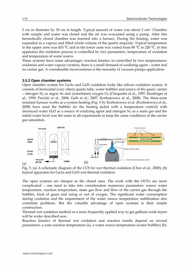
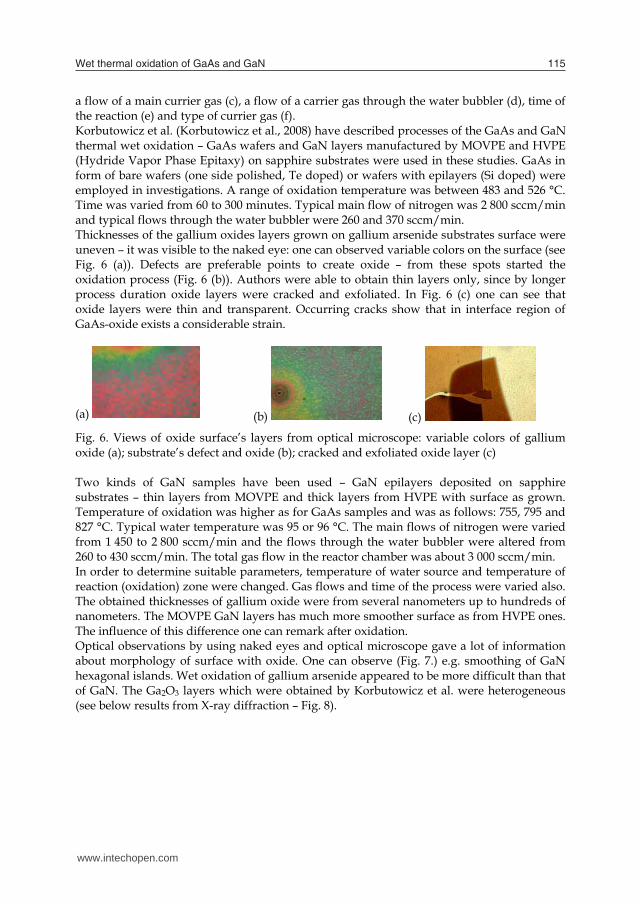
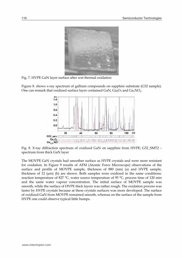


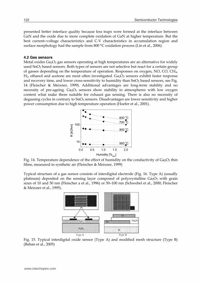

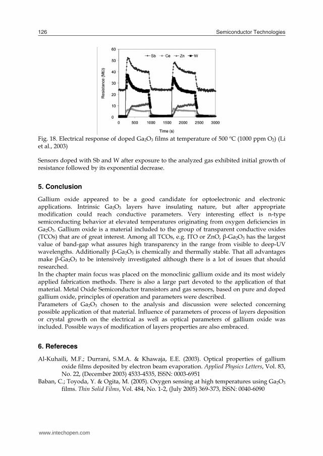


![Ryszard Groń - bazhum.muzhp.plbazhum.muzhp.pl/media//files/Wroclawski_Przeglad...Ryszard Groń "The Historical Works", Aelred of Rievaulx, Kalamazoo 2005 : [recenzja] Wrocławski](https://static.documents.pub/doc/80x56/6129f80fbc7ea15dc56c6c8e/ryszard-gro-ryszard-gro-the-historical-works-aelred-of-rievaulx.jpg)

