The term “combinational” comes to us from mathematics. In mathematics a combination is an unordered set, which is a formal way to say that nobody cares which order the items came in. Most games work this way, if you rolled dice one at a time and get a 2 followed by a 3 it is the same as if you had rolled a 3 followed by a 2. With combinational logic, the circuit produces the same output regardless of the order the inputs are changed. There are circuits which depend on the when the inputs change, these circuits are called sequential logic. Even though you will not find the term “sequential logic” in the chapter titles, the next several chapters will discuss sequential logic. Practical circuits will have a mix of combinational and sequential logic, with sequential logic making sure everything happens in order and combinational logic performing functions like arithmetic, logic, or conversion. You have already used combinational circuits. Each logic gate discussed previously is a combinational logic function. Let’s follow how two NAND gate works if we provide them inputs in different orders. We begin with both inputs being 0.
Transcript
The term “combinational” comes to us from mathematics. In mathematics acombination is an unordered set, which is a formal way to say that nobody careswhich order the items came in. Most games work this way, if you rolled dice oneat a time and get a 2 followed by a 3 it is the same as if you had rolled a 3followed by a 2. With combinational logic, the circuit produces the same outputregardless of the order the inputs are changed.
There are circuits which depend on the when the inputs change, thesecircuits are called sequential logic. Even though you will not find the term“sequential logic” in the chapter titles, the next several chapters will discusssequential logic.
Practical circuits will have a mix of combinational and sequential logic,with sequential logic making sure everything happens in order and combinationallogic performing functions like arithmetic, logic, or conversion.
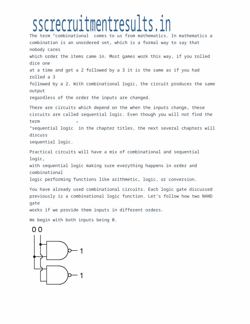
You have already used combinational circuits. Each logic gate discussedpreviously is a combinational logic function. Let’s follow how two NAND gateworks if we provide them inputs in different orders.
We begin with both inputs being 0.
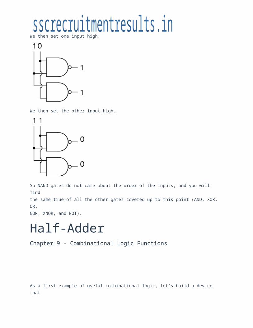
We then set one input high.
We then set the other input high.
So NAND gates do not care about the order of the inputs, and you will findthe same true of all the other gates covered up to this point (AND, XOR, OR,NOR, XNOR, and NOT).
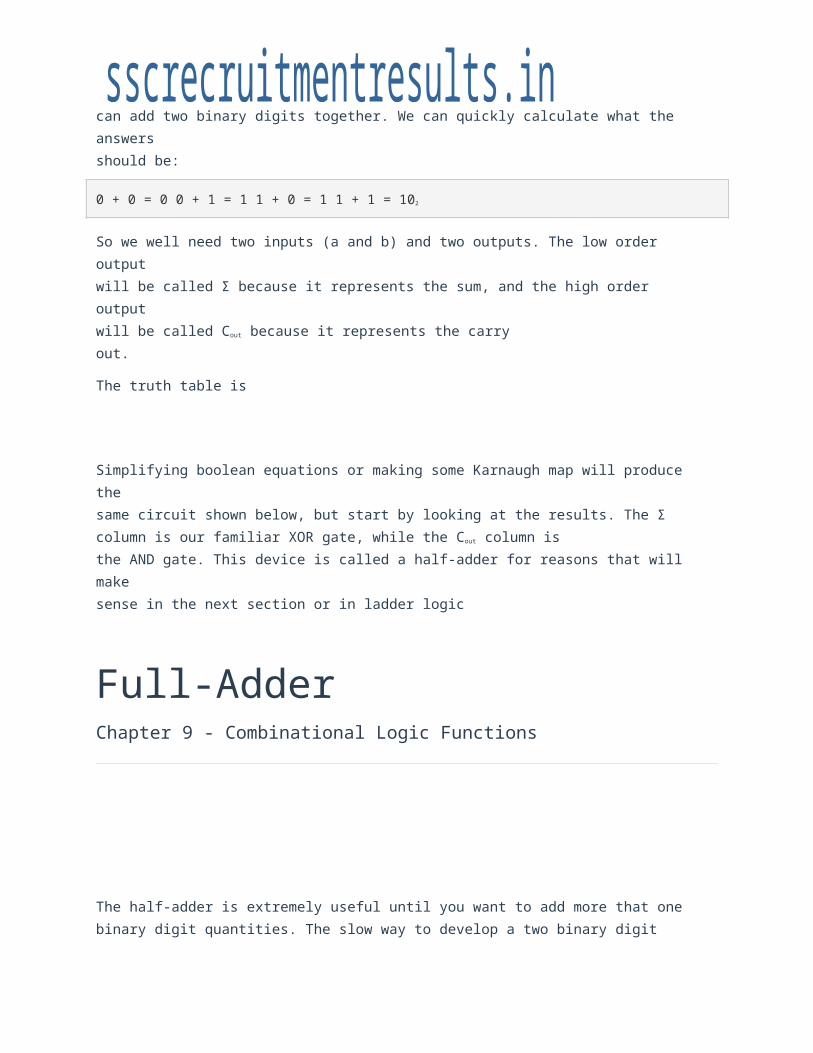
As a first example of useful combinational logic, let’s build a device thatcan add two binary digits together. We can quickly calculate what the answersshould be:
0 + 0 = 0 0 + 1 = 1 1 + 0 = 1 1 + 1 = 102
So we well need two inputs (a and b) and two outputs. The low order outputwill be called Σ because it represents the sum, and the high order outputwill be called Cout because it represents the carryout.
The truth table is
Simplifying boolean equations or making some Karnaugh map will produce thesame circuit shown below, but start by looking at the results. The Σcolumn is our familiar XOR gate, while the Cout column isthe AND gate. This device is called a half-adder for reasons that will makesense in the next section or in ladder logic
The half-adder is extremely useful until you want to add more that onebinary digit quantities. The slow way to develop a two binary digit adders wouldbe to make a truth table and reduce it. Then when you decide to make a threebinary digit adder, do it again. Then when you decide to make a four digitadder, do it again. Then when ... The circuits would be fast, but developmenttime would be slow.
Looking at a two binary digit sum shows what we need to extend addition tomultiple binary digits.
11 11 11 --- 110
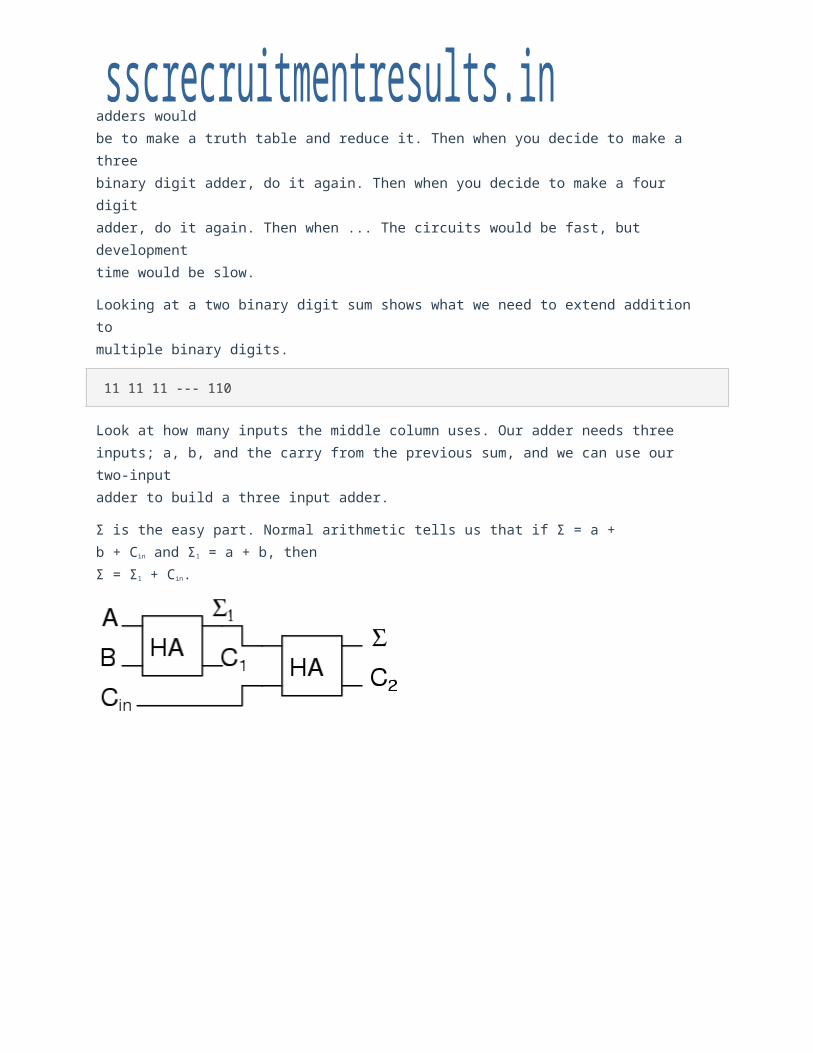
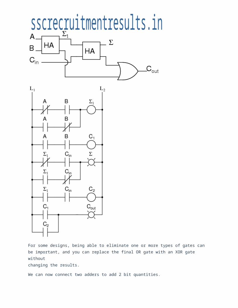
Look at how many inputs the middle column uses. Our adder needs threeinputs; a, b, and the carry from the previous sum, and we can use our two-inputadder to build a three input adder.
Σ is the easy part. Normal arithmetic tells us that if Σ = a +b + Cin and Σ1 = a + b, thenΣ = Σ1 + Cin.
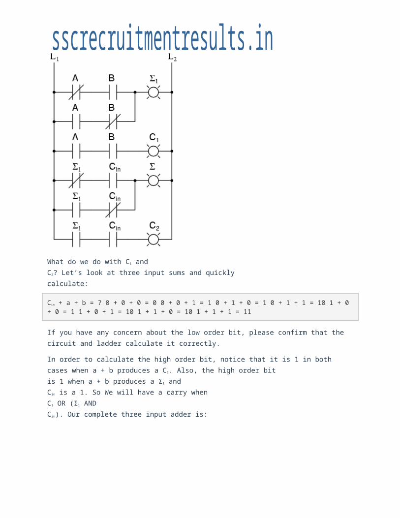
What do we do with C1 andC2? Let’s look at three input sums and quicklycalculate:
If you have any concern about the low order bit, please confirm that thecircuit and ladder calculate it correctly.
In order to calculate the high order bit, notice that it is 1 in bothcases when a + b produces a C1. Also, the high order bitis 1 when a + b produces a Σ1 andCin is a 1. So We will have a carry whenC1 OR (Σ1 ANDCin). Our complete three input adder is:
For some designs, being able to eliminate one or more types of gates canbe important, and you can replace the final OR gate with an XOR gate withoutchanging the results.
We can now connect two adders to add 2 bit quantities.
A0 is the low order bit of A,A1 is the high order bit of A, B0
is the low order bit of B, B1 is the high order bit of B,Σ0is the low order bit of the sum,Σ1 is the high order bit of the sum, andCout is the Carry.
A two binary digit adder would never be made this way. Instead the lowestorder bits would also go through a full adder.
There are several reasons for this, one being that we can then allow acircuit to determine whether the lowest order carry should be included in thesum. This allows for the chaining of even larger sums. Consider two differentways to look at a four bit sum.
If we allow the program to add a two bit number and remember the carry for later, then use that carry in the next sum the program can add any number of bits the user wants even though we have only provided a two-bit adder. Small PLCs can also be chained together for larger numbers. These full adders can also can be expanded to any number of bits space allows. As an example, here’s how to do an 8 bit adder.
This is the same result as using the two 2-bit adders to make a 4-bit adder and then using two 4-bit adders to make an 8-bit adder or re-duplicating ladder logic and updating the numbers.
Each “2+” is a 2-bit adder and made of two full adders. Each “4+” is a 4-bit adder and made of two 2-bit adders. And the result of two 4-bit adders is the same 8-bit adder we used full adders to build. For any large combinational circuit there are generally two approaches to design: you can take simpler circuits and replicate them; or you can design the complex circuit as a complete device. Using simpler circuits to build complex circuits allows a you to spend less time designing but then requires more time for signals to propagate through the transistors. The 8-bit adder design above has to wait for all the Cxoutsignals to move from A0 + B0 up to the inputs of Σ7. If a designer builds an 8-bit adder as a complete device simplified to a sum of products, then each signal just travels through one NOT gate, one AND gate and one OR gate. A seventeen input device has a truth
table with 131,072 entries, and reducing 131,072 entries to a sum of products will take some time. When designing for systems that have a maximum allowed response time to provide the final result, you can begin by using simpler circuits and then attempt to replace portions of the circuit that are too slow. That way you spend most of your time on the portions of a circuit that matter.
DecoderChapter 9 - Combinational Logic Functions
A decoder is a circuit that changes a code into a set of signals. It is called a decoder because it does the reverse of encoding, but we will begin our study of encoders and decoders with decoders because they are simpler to design.
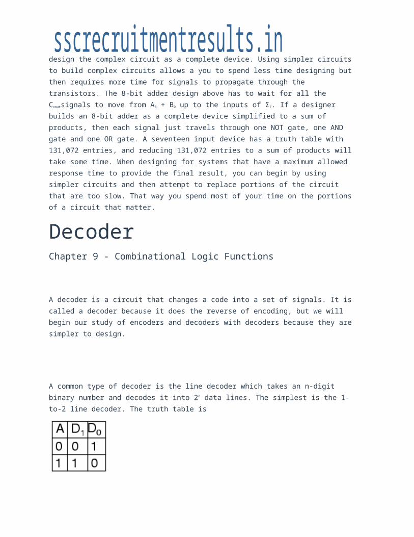
A common type of decoder is the line decoder which takes an n-digit binary number and decodes it into 2n data lines. The simplest is the 1-to-2 line decoder. The truth table is
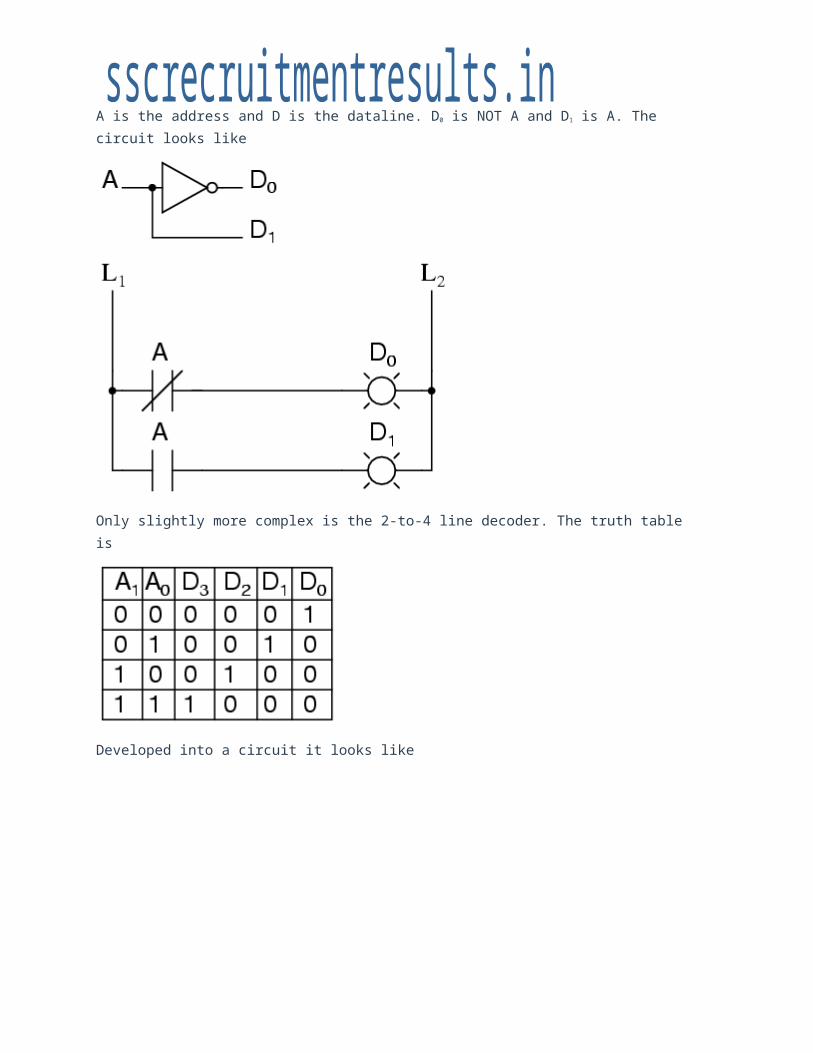
A is the address and D is the dataline. D0 is NOT A and D1 is A. The circuit looks like
Only slightly more complex is the 2-to-4 line decoder. The truth table is
Developed into a circuit it looks like
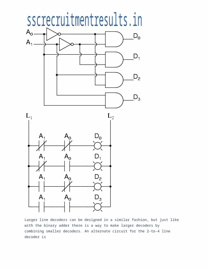
Larger line decoders can be designed in a similar fashion, but just like with the binary adder there is a way to make larger decoders by combining smaller decoders. An alternate circuit for the 2-to-4 line decoder is
Replacing the 1-to-2 Decoders with their circuits will show that both circuits are equivalent. In a similar fashion a 3-to-8 line decoder can be made from a 1-to-2 line decoder and a 2-to-4 line decoder, and a 4-to-16 line decoder can be made from two 2-to-4 line decoders.
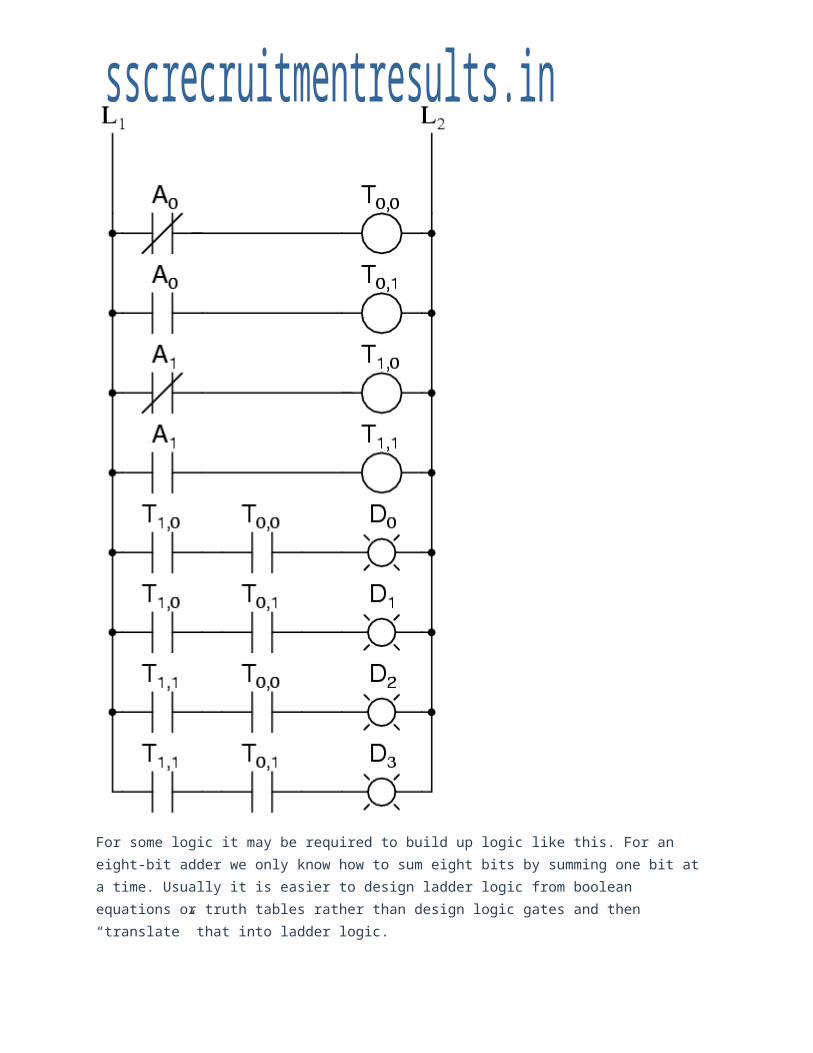
You might also consider making a 2-to-4 decoder ladder from 1-to-2 decoder ladders. If you do it might look something like this:
For some logic it may be required to build up logic like this. For an eight-bit adder we only know how to sum eight bits by summing one bit at a time. Usually it is easier to design ladder logic from boolean equations or truth tables rather than design logic gates and then “translate” that into ladder logic.
A typical application of a line decoder circuit is to select among multiple devices. A circuit needing to select among sixteen devices could have sixteen control lines to select which device should “listen”. With a decoder only four control lines are needed.
EncoderChapter 9 - Combinational Logic Functions
An encoder is a circuit that changes a set of signals into a code. Let’sbegin making a 2-to-1 line encoder truth table by reversing the 1-to-2 decodertruth table.
This truth table is a little short. A complete truth table would be
One question we need to answer is what to do with those other inputs? Dowe ignore them? Do we have them generate an additional error output? In manycircuits this problem is solved by adding sequential logic in order to know notjust what input is active but also which order the inputs became active.
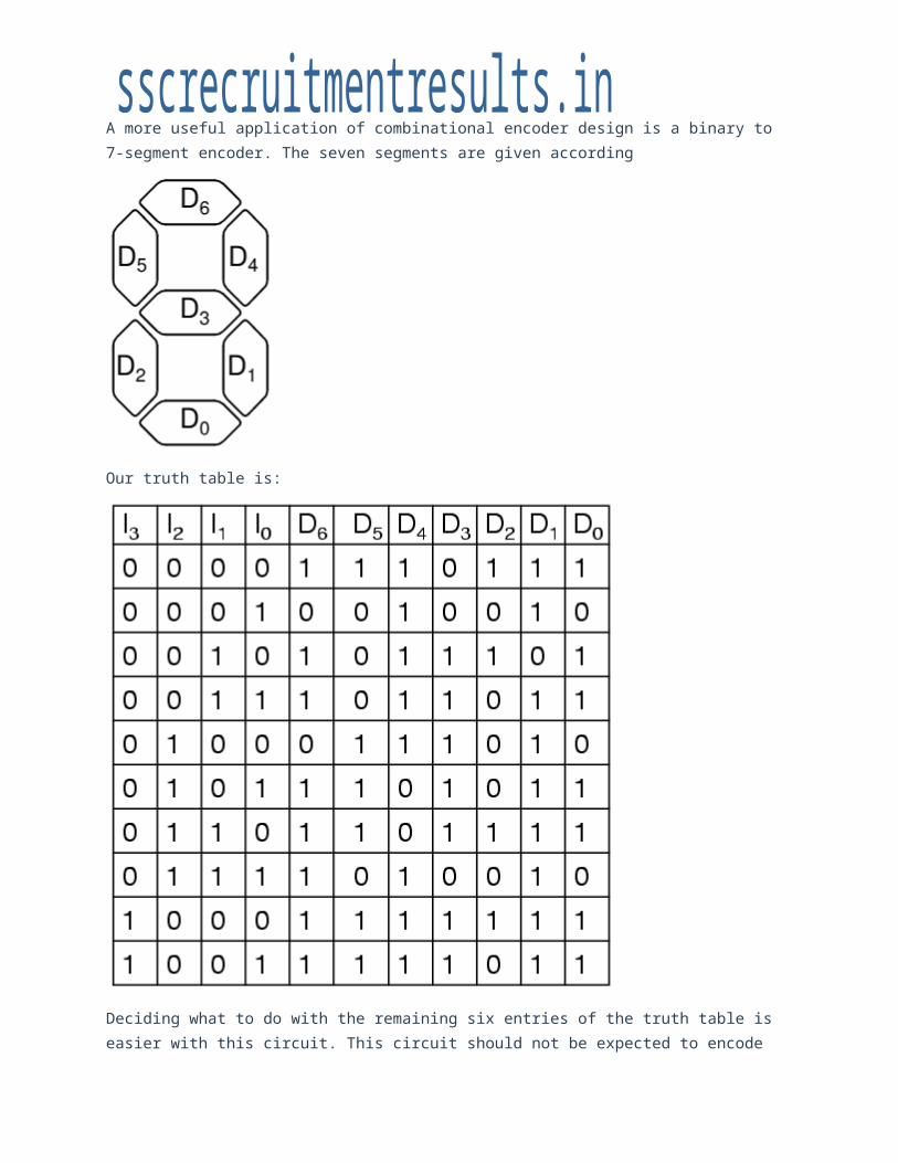
A more useful application of combinational encoder design is a binary to7-segment encoder. The seven segments are given according
Our truth table is:
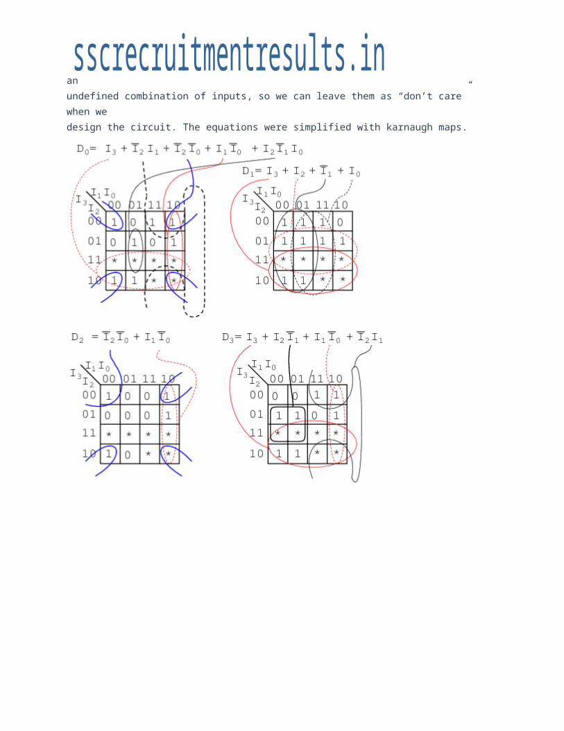
Deciding what to do with the remaining six entries of the truth table iseasier with this circuit. This circuit should not be expected to encode an
undefined combination of inputs, so we can leave them as “don’t care” when wedesign the circuit. The equations were simplified with karnaugh maps.