Page 1
Cover
Embest S3CEV40 EVB
User Guide
Version 2.1
Embest Info&Tech Co.,LTD. All rights reserved.
Room 210, Luohu Science&Technology Building,
#85 Taining Road, Shenzhen, Guangdong, China
Tel: +86-755-25635626/25635656/25631365 Fax: +86-755-25616057
E-mail: [email protected] [email protected]
http://www.embedinfo.com
Copyright ©2001-2004 Embest Info&Tech Co.,LTD. All rights reserved.
Page 2
Content
FOREWORD..................................................................................................................3
CHAPTER I INTRODUCTION TO EMBEST S3CEV40 .................................................4
1.1 Overview........................................................................................................................4
1.2 Embest S3CEV40 Development Kit ..............................................................................5
1.3 Features of Embest S3CEV40........................................................................................6
CHAPTER II INSTALLATION AND USE ......................................................................7
2.1 Structure of Embest S3CEV40 Development Board......................................................7
2.2 Power Supply of Embest S3CEV40...............................................................................8
2.3 JTAG Connection...........................................................................................................9
2.4 Serial Port Connection .................................................................................................10
2.5 Hardware Testing .........................................................................................................11
CHAPTER III HARDWARE STRUCTURE .......................................................................19
3.1 Electric circuit structure .................................................................................................19
3.2 Core Electric Circuit ......................................................................................................20
3.3 Embest S3CEV40 Communication Port Circuit ............................................................25
3.4 External Expanded Module............................................................................................28
3.5 I/O usage ........................................................................................................................33
3.6 Bus Expansion................................................................................................................37
CHAPTER IV SOFTWARE SYSTEM ...........................................................................38
4.2 Introduction to Start Program.........................................................................................42
4.3 µCOS-II..........................................................................................................................50
4.4 Example Codes ..............................................................................................................59
CHAPTER V CUSTOMER SERVICE ............................................................................61
APPENDIX A JUMPER AND SWITCH SET ..................................................................62
Copyright ©2001-2004 Embest Info&Tech Co.,LTD. All rights reserved. Page 2
Page 3
Foreword
This manual is prepared for users of Embest S3CV40 development board of
Embest Info & Tech Co., Ltd. The manual contains the following chapters:
Chapter I Introduction to Embest S3CEV40
Chapter II Installation and Use
Chapter III Hardware Structure of Embest S3CEV40 Board
Chapter IV Software System of Embest S3CEV40
Chapter V After-sales Service and Technical Support
Appendix Jumper and Switch Setting
When using the Embest S3CEV40 development board and the Manual, the
user can also refer to the circuit diagram (included in the CD enclosed).
Due to the limited time, errors may exist in this manual. We are open to
any corrections from readers. Thank you!
Copywrite©2003 by Shenzhen Embest Info&Tech Co.,LTD.
All rights reserved.
No part of this document may be reproducted or transmitted in any form or
by any means without prior written consent of Embest Info&Tech Co.,LTD.
Embest® is registered trademarks of Embest Info&Tech Co.,LTD.
Copyright ©2001-2004 Embest Info&Tech Co.,LTD. All rights reserved. Page 3
Page 4
Chapter I Introduction to Embest S3CEV40
1.1 Overview
Embest S3CEV40 development board is an all-purpose ARM development
board developed by Shenzhen Embest Info & Tech Co., Ltd. It is the best choice
for designing reference , development and application of Samsung S3C44B0x
processor(ARM7TDMI RISC CPU core). It is also an ideal platform for learning
& teaching of ARM and embedded software.
Embest S3CEV40 development board hardware system includes memory,
I/O, digital LED, LCD, touch screen, keyboard and audio output.
Communication interfaces include serial ports, Ethernet interface, USB
interface and I2C interface. Advanced extension includes IDE disk, CF card and
a Flash electronic disk. It is an all-purpose development board with a complete
set of interfaces.
Embest S3CEV40 development board has a multi-functional test program
and driver with uCOS-II and uCLinux real-time operating system already
installed. Embest S3CEV40 development board provides a standard 20-pin
JTAG interface with which the user can fully control CPU and test the program
via JTAG.
Copyright ©2001-2004 Embest Info&Tech Co.,LTD. All rights reserved. Page 4
Page 5
1.2 Embest S3CEV40 Development Kit
A complete set of Embest S3CEV40 development kit includes:
Embest S3CEV40 development board
RS232 serial port line
5V DC power adapter
USB line
Embest S3CEV40 CD-ROM:
- Manual
- Circuit diagram
- Start program and functional module test programs
- All source programs of real-time operating system uCOS-II
When opening the package, please check if any of the above items is
missing. If so, please contact your distributor right away.
Copyright ©2001-2004 Embest Info&Tech Co.,LTD. All rights reserved. Page 5
Page 6
1.3 Features of Embest S3CEV40
Hardware specification:
5.0V DC or USB power supply
2 M bytes 16-bit Flash
8 M bytes 16-bit SDRAM
4K bit EEPROM with IIC BUS
2x RS232
USB connecter
10M Ethernet interface connector
microphone input
IIS audio frequency output (speaker out)
16 M Bytes Nand Flash
External IDE port
LCD&TSP touch screen port
320×240 LCD * (optional)
4×4 keyboard * (optional)
Reset button
2 interrupt buttons and 2 LEDS
8 segment leds
20-pin JTAG interface connector
4 groups 2×20 PIN expansion connectors of CPU
Copyright ©2001-2004 Embest Info&Tech Co.,LTD. All rights reserved. Page 6
Page 7
Chapter II Installation and Use
This chapter is mainly an introduction to how to install and connect the
Embest S3CEV40 development board, and how to conduct basic software and
hardware testing.
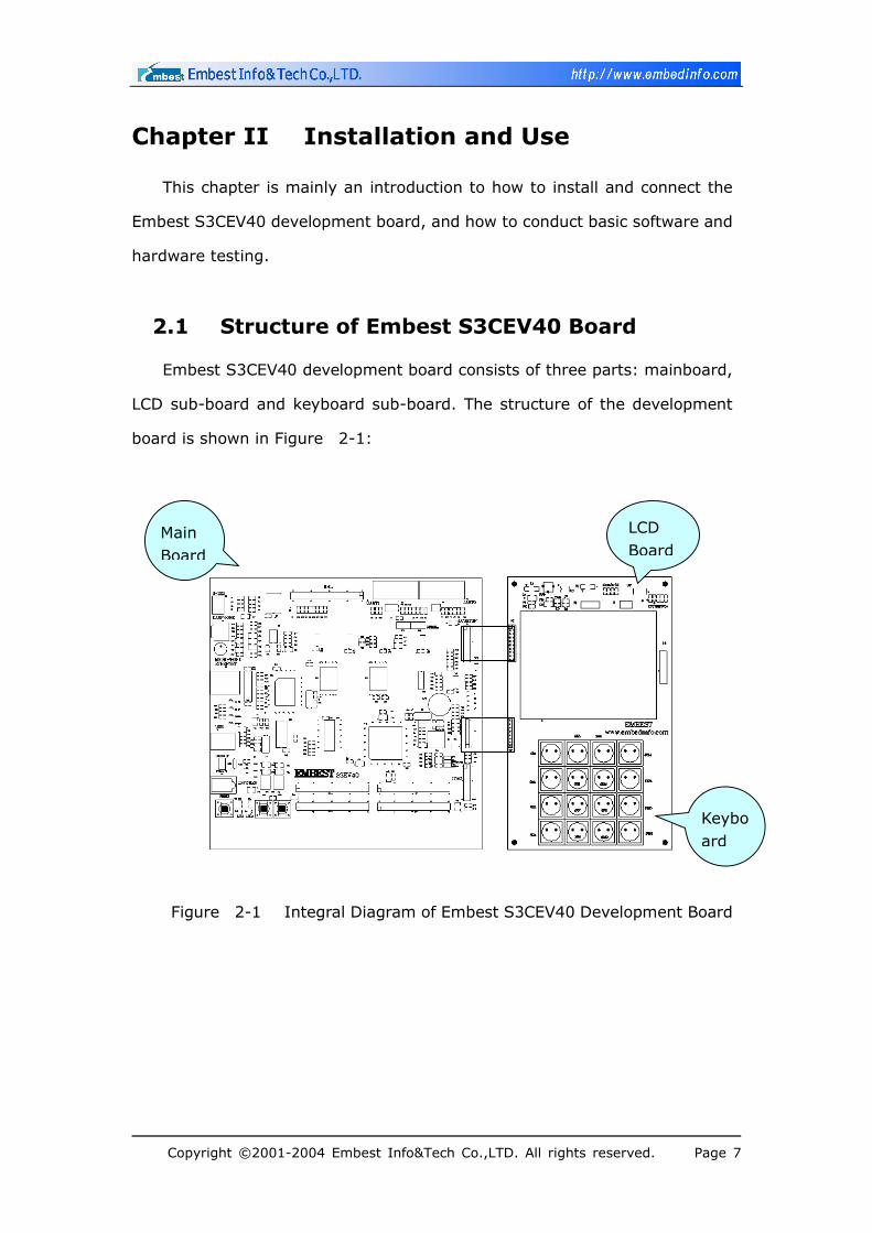
2.1 Structure of Embest S3CEV40 Board
Embest S3CEV40 development board consists of three parts: mainboard,
LCD sub-board and keyboard sub-board. The structure of the development
board is shown in Figure 2-1:
Main Board
LCD Board
Keyboard
Figure 2-1 Integral Diagram of Embest S3CEV40 Development Board
Copyright ©2001-2004 Embest Info&Tech Co.,LTD. All rights reserved. Page 7
Page 8
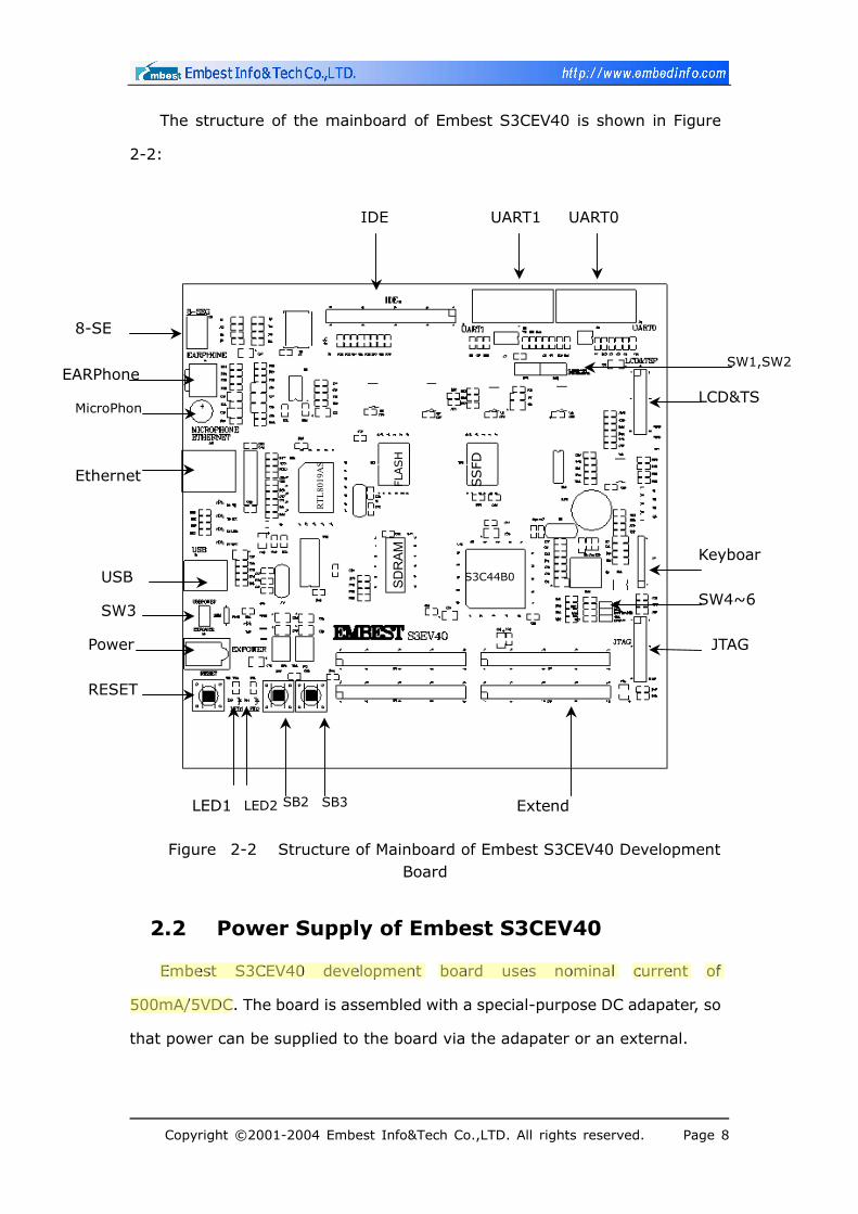
The structure of the mainboard of Embest S3CEV40 is shown in Figure
2-2:
IDE UART1 UART0
8-SE
SW1,SW2 EARPhone
LCD&TSMicroPhon
SSFD
FLASH
RTL8
019A
S
Ethernet
SD
RA
M
KeyboarUSB S3C44B0
SW4~6SW3
Power JTAG
RESET
LED2 SB3 SB2 Extend
LED1
Figure 2-2 Structure of Mainboard of Embest S3CEV40 Development Board
2.2 Power Supply of Embest S3CEV40
Embest S3CEV40 development board uses nominal current of
500mA/5VDC. The board is assembled with a special-purpose DC adapater, so
that power can be supplied to the board via the adapater or an external.
Copyright ©2001-2004 Embest Info&Tech Co.,LTD. All rights reserved. Page 8
Page 9
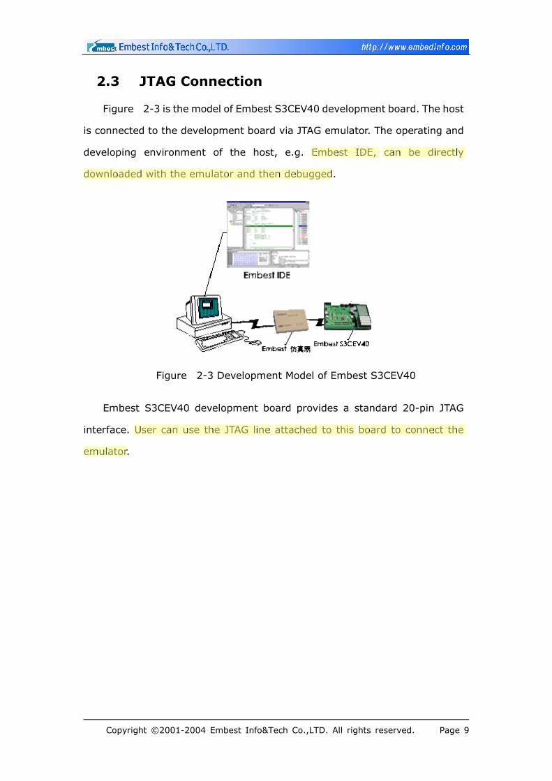
2.3 JTAG Connection
Figure 2-3 is the model of Embest S3CEV40 development board. The host
is connected to the development board via JTAG emulator. The operating and
developing environment of the host, e.g. Embest IDE, can be directly
downloaded with the emulator and then debugged.
Figure 2-3 Development Model of Embest S3CEV40
Embest S3CEV40 development board provides a standard 20-pin JTAG
interface. User can use the JTAG line attached to this board to connect the
emulator.
Copyright ©2001-2004 Embest Info&Tech Co.,LTD. All rights reserved. Page 9
Page 10
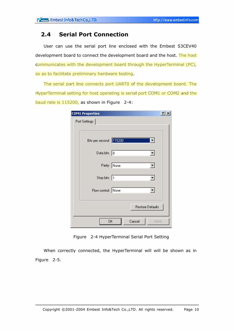
2.4 Serial Port Connection
User can use the serial port line enclosed with the Embest S3CEV40
development board to connect the development board and the host. The host
communicates with the development board through the HyperTerminal (PC),
so as to facilitate preliminary hardware testing.
The serial port line connects port UART0 of the development board. The
HyperTerminal setting for host operating is serial port COM1 or COM2 and the
baud rate is 115200, as shown in Figure 2-4:
Figure 2-4 HyperTerminal Serial Port Setting
When correctly connected, the HyperTerminal will will be shown as in
Figure 2-5.
Copyright ©2001-2004 Embest Info&Tech Co.,LTD. All rights reserved. Page 10
Page 11
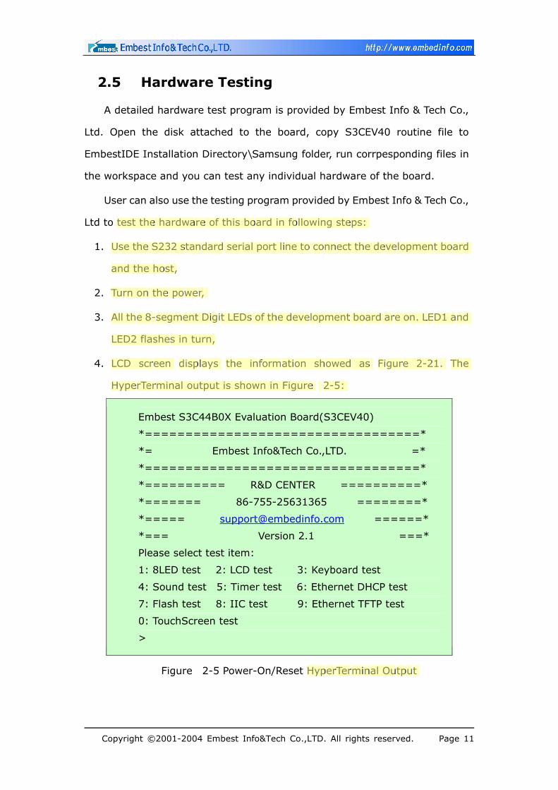
2.5 Hardware Testing
A detailed hardware test program is provided by Embest Info & Tech Co.,
Ltd. Open the disk attached to the board, copy S3CEV40 routine file to
EmbestIDE Installation Directory\Samsung folder, run corrpesponding files in
the workspace and you can test any individual hardware of the board.
User can also use the testing program provided by Embest Info & Tech Co.,
Ltd to test the hardware of this board in following steps:
1. Use the S232 standard serial port line to connect the development board
and the host,
2. Turn on the power,
3. All the 8-segment Digit LEDs of the development board are on. LED1 and
LED2 flashes in turn,
4. LCD screen displays the information showed as Figure 2-21. The
HyperTerminal output is shown in Figure 2-5:
Embest S3C44B0X Evaluation Board(S3CEV40)
*==================================*
*= Embest Info&Tech Co.,LTD. =*
*==================================*
*========== R&D CENTER ==========*
*======= 86-755-25631365 ========*
*===== [email protected] ======*
*=== Version 2.1 ===*
Please select test item:
1: 8LED test 2: LCD test 3: Keyboard test
4: Sound test 5: Timer test 6: Ethernet DHCP test
7: Flash test 8: IIC test 9: Ethernet TFTP test
0: TouchScreen test
>
Figure 2-5 Power-On/Reset HyperTerminal Output
Copyright ©2001-2004 Embest Info&Tech Co.,LTD. All rights reserved. Page 11
Page 12
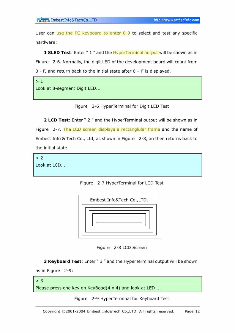
User can use the PC keyboard to enter 0-9 to select and test any specific
hardware:
1 8LED Test: Enter “ 1 ” and the HyperTerminal output will be shown as in
Figure 2-6. Normally, the digit LED of the development board will count from
0 - F, and return back to the initial state after 0 – F is displayed.
> 1
Look at 8-segment Digit LED...
Figure 2-6 HyperTerminal for Digit LED Test
2 LCD Test: Enter “ 2 ” and the HyperTerminal output will be shown as in
Figure 2-7. The LCD screen displays a rectanglular frame and the name of
Embest Info & Tech Co., Ltd, as shown in Figure 2-8, an then returns back to
the initial state.
> 2
Look at LCD...
Figure 2-7 HyperTerminal for LCD Test
Embest Info&Tech Co.,LTD.
Figure 2-8 LCD Screen
3 Keyboard Test: Enter “ 3 ” and the HyperTerminal output will be shown
as in Figure 2-9:
> 3
Please press one key on KeyBoad(4 x 4) and look at LED ...
Figure 2-9 HyperTerminal for Keyboard Test
Copyright ©2001-2004 Embest Info&Tech Co.,LTD. All rights reserved. Page 12
Page 13
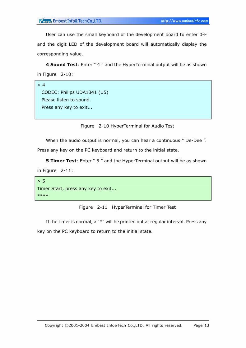
User can use the small keyboard of the development board to enter 0-F
and the digit LED of the development board will automatically display the
corresponding value.
4 Sound Test: Enter “ 4 ” and the HyperTerminal output will be as shown
in Figure 2-10:
> 4
CODEC: Philips UDA1341 (U5)
Please listen to sound.
Press any key to exit...
Figure 2-10 HyperTerminal for Audio Test
When the audio output is normal, you can hear a continuous “ De-Dee ”.
Press any key on the PC keyboard and return to the initial state.
5 Timer Test: Enter “ 5 ” and the HyperTerminal output will be as shown
in Figure 2-11:
> 5
Timer Start, press any key to exit...
****
Figure 2-11 HyperTerminal for Timer Test
If the timer is normal, a “*” will be printed out at regular interval. Press any
key on the PC keyboard to return to the initial state.
Copyright ©2001-2004 Embest Info&Tech Co.,LTD. All rights reserved. Page 13
Page 14
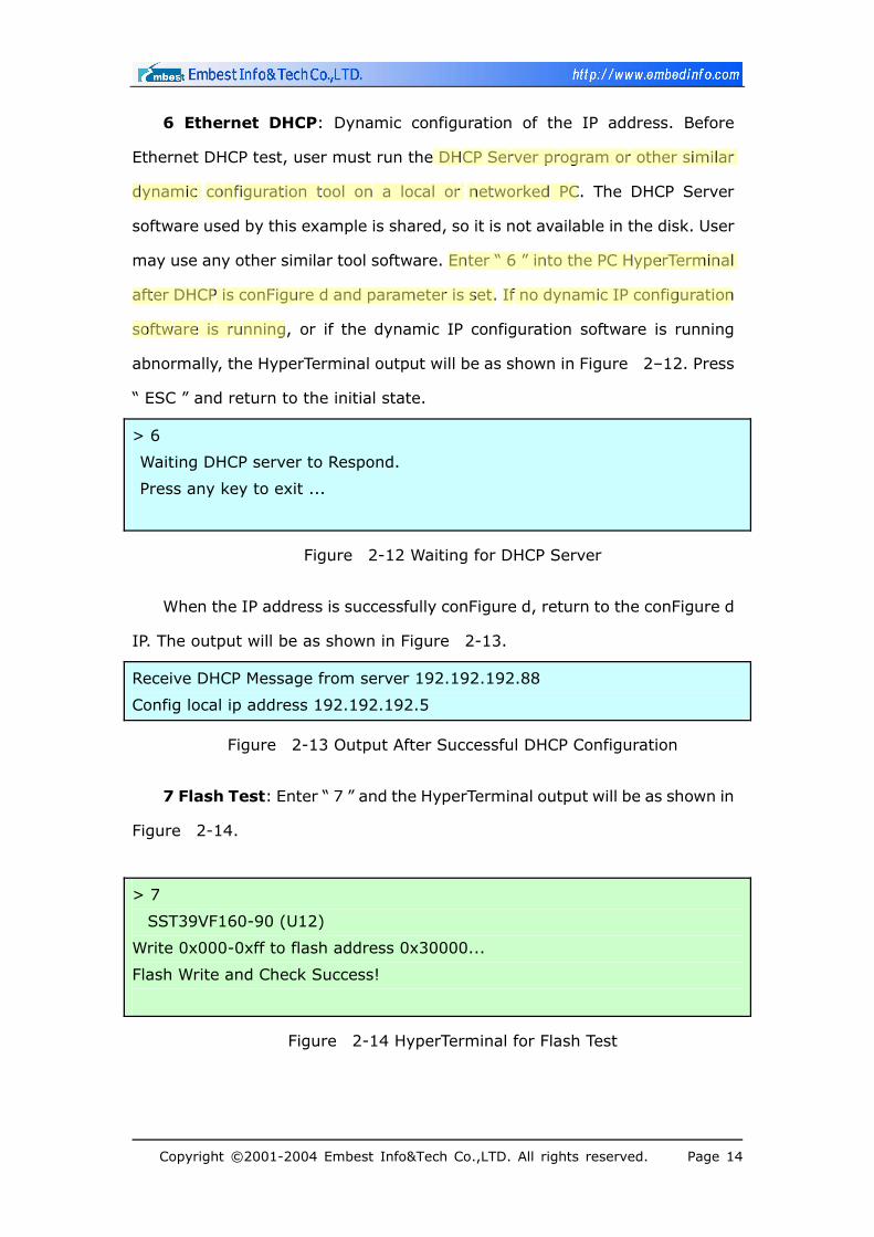
6 Ethernet DHCP: Dynamic configuration of the IP address. Before
Ethernet DHCP test, user must run the DHCP Server program or other similar
dynamic configuration tool on a local or networked PC. The DHCP Server
software used by this example is shared, so it is not available in the disk. User
may use any other similar tool software. Enter “ 6 ” into the PC HyperTerminal
after DHCP is conFigure d and parameter is set. If no dynamic IP configuration
software is running, or if the dynamic IP configuration software is running
abnormally, the HyperTerminal output will be as shown in Figure 2–12. Press
“ ESC ” and return to the initial state.
> 6
Waiting DHCP server to Respond.
Press any key to exit ...
Figure 2-12 Waiting for DHCP Server
When the IP address is successfully conFigure d, return to the conFigure d
IP. The output will be as shown in Figure 2-13.
Receive DHCP Message from server 192.192.192.88
Config local ip address 192.192.192.5
Figure 2-13 Output After Successful DHCP Configuration
7 Flash Test: Enter “ 7 ” and the HyperTerminal output will be as shown in
Figure 2-14.
> 7
SST39VF160-90 (U12)
Write 0x000-0xff to flash address 0x30000...
Flash Write and Check Success!
Figure 2-14 HyperTerminal for Flash Test
Copyright ©2001-2004 Embest Info&Tech Co.,LTD. All rights reserved. Page 14
Page 15
Sequentially write 0x00-0xff into Flash address (0x30000). Read and
compare. When it is successful, the “ Success” prompt will be displayed. Press
any key on the PC to return to the initial state.
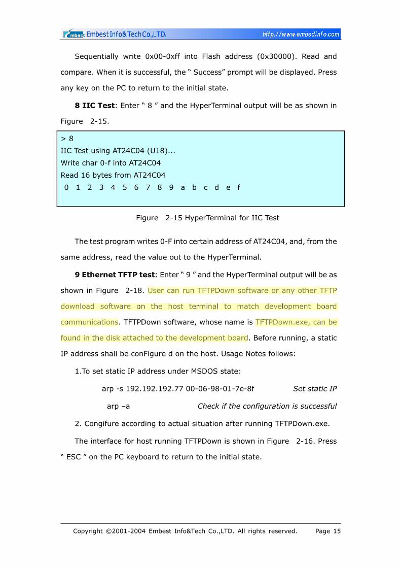
8 IIC Test: Enter “ 8 ” and the HyperTerminal output will be as shown in
Figure 2-15.
> 8
IIC Test using AT24C04 (U18)...
Write char 0-f into AT24C04
Read 16 bytes from AT24C04
0 1 2 3 4 5 6 7 8 9 a b c d e f
Figure 2-15 HyperTerminal for IIC Test
The test program writes 0-F into certain address of AT24C04, and, from the
same address, read the value out to the HyperTerminal.
9 Ethernet TFTP test: Enter “ 9 ” and the HyperTerminal output will be as
shown in Figure 2-18. User can run TFTPDown software or any other TFTP
download software on the host terminal to match development board
communications. TFTPDown software, whose name is TFTPDown.exe, can be
found in the disk attached to the development board. Before running, a static
IP address shall be conFigure d on the host. Usage Notes follows:
1.To set static IP address under MSDOS state:
arp -s 192.192.192.77 00-06-98-01-7e-8f Set static IP
arp –a Check if the configuration is successful
2. Congifure according to actual situation after running TFTPDown.exe.
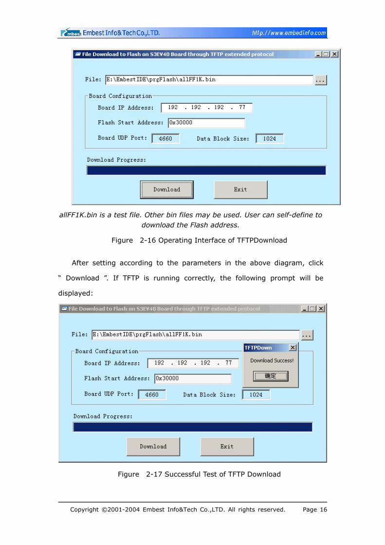
The interface for host running TFTPDown is shown in Figure 2-16. Press
“ ESC ” on the PC keyboard to return to the initial state.
Copyright ©2001-2004 Embest Info&Tech Co.,LTD. All rights reserved. Page 15
Page 16
allFF1K.bin is a test file. Other bin files may be used. User can self-define to download the Flash address.
Figure 2-16 Operating Interface of TFTPDownload
After setting according to the parameters in the above diagram, click
“ Download ”. If TFTP is running correctly, the following prompt will be
displayed:
Figure 2-17 Successful Test of TFTP Download
Copyright ©2001-2004 Embest Info&Tech Co.,LTD. All rights reserved. Page 16
Page 17
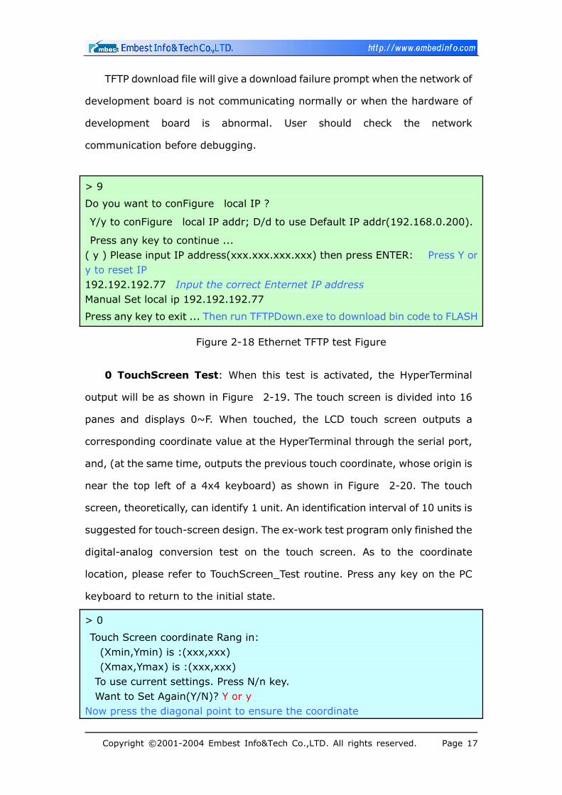
TFTP download file will give a download failure prompt when the network of
development board is not communicating normally or when the hardware of
development board is abnormal. User should check the network
communication before debugging.
> 9
Do you want to conFigure local IP ?
Y/y to conFigure local IP addr; D/d to use Default IP addr(192.168.0.200).
Press any key to continue ... ( y ) Please input IP address(xxx.xxx.xxx.xxx) then press ENTER: Press Y or y to reset IP 192.192.192.77 Input the correct Enternet IP address Manual Set local ip 192.192.192.77
Press any key to exit ... Then run TFTPDown.exe to download bin code to FLASH
Figure 2-18 Ethernet TFTP test Figure
0 TouchScreen Test: When this test is activated, the HyperTerminal
output will be as shown in Figure 2-19. The touch screen is divided into 16
panes and displays 0~F. When touched, the LCD touch screen outputs a
corresponding coordinate value at the HyperTerminal through the serial port,
and, (at the same time, outputs the previous touch coordinate, whose origin is
near the top left of a 4x4 keyboard) as shown in Figure 2-20. The touch
screen, theoretically, can identify 1 unit. An identification interval of 10 units is
suggested for touch-screen design. The ex-work test program only finished the
digital-analog conversion test on the touch screen. As to the coordinate
location, please refer to TouchScreen_Test routine. Press any key on the PC
keyboard to return to the initial state.
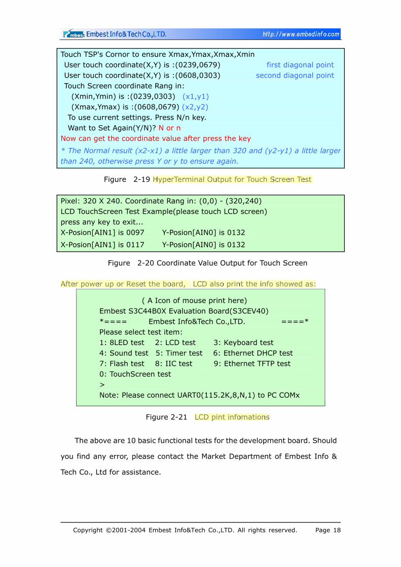
> 0
Touch Screen coordinate Rang in: (Xmin,Ymin) is :(xxx,xxx) (Xmax,Ymax) is :(xxx,xxx) To use current settings. Press N/n key. Want to Set Again(Y/N)? Y or y Now press the diagonal point to ensure the coordinate
Copyright ©2001-2004 Embest Info&Tech Co.,LTD. All rights reserved. Page 17
Page 18
Touch TSP's Cornor to ensure Xmax,Ymax,Xmax,Xmin User touch coordinate(X,Y) is :(0239,0679) first diagonal point User touch coordinate(X,Y) is :(0608,0303) second diagonal point Touch Screen coordinate Rang in: (Xmin,Ymin) is :(0239,0303) (x1,y1) (Xmax,Ymax) is :(0608,0679) (x2,y2) To use current settings. Press N/n key. Want to Set Again(Y/N)? N or n Now can get the coordinate value after press the key
* The Normal result (x2-x1) a little larger than 320 and (y2-y1) a little larger than 240, otherwise press Y or y to ensure again.
Figure 2-19 HyperTerminal Output for Touch Screen Test
Pixel: 320 X 240. Coordinate Rang in: (0,0) - (320,240) LCD TouchScreen Test Example(please touch LCD screen) press any key to exit... X-Posion[AIN1] is 0097 Y-Posion[AIN0] is 0132
X-Posion[AIN1] is 0117 Y-Posion[AIN0] is 0132
Figure 2-20 Coordinate Value Output for Touch Screen
After power up or Reset the board, LCD also print the info showed as:
( A Icon of mouse print here) Embest S3C44B0X Evaluation Board(S3CEV40) *==== Embest Info&Tech Co.,LTD. ====* Please select test item: 1: 8LED test 2: LCD test 3: Keyboard test 4: Sound test 5: Timer test 6: Ethernet DHCP test 7: Flash test 8: IIC test 9: Ethernet TFTP test 0: TouchScreen test > Note: Please connect UART0(115.2K,8,N,1) to PC COMx
Figure 2-21 LCD pint infomations
The above are 10 basic functional tests for the development board. Should
you find any error, please contact the Market Department of Embest Info &
Tech Co., Ltd for assistance.
Copyright ©2001-2004 Embest Info&Tech Co.,LTD. All rights reserved. Page 18
Page 19
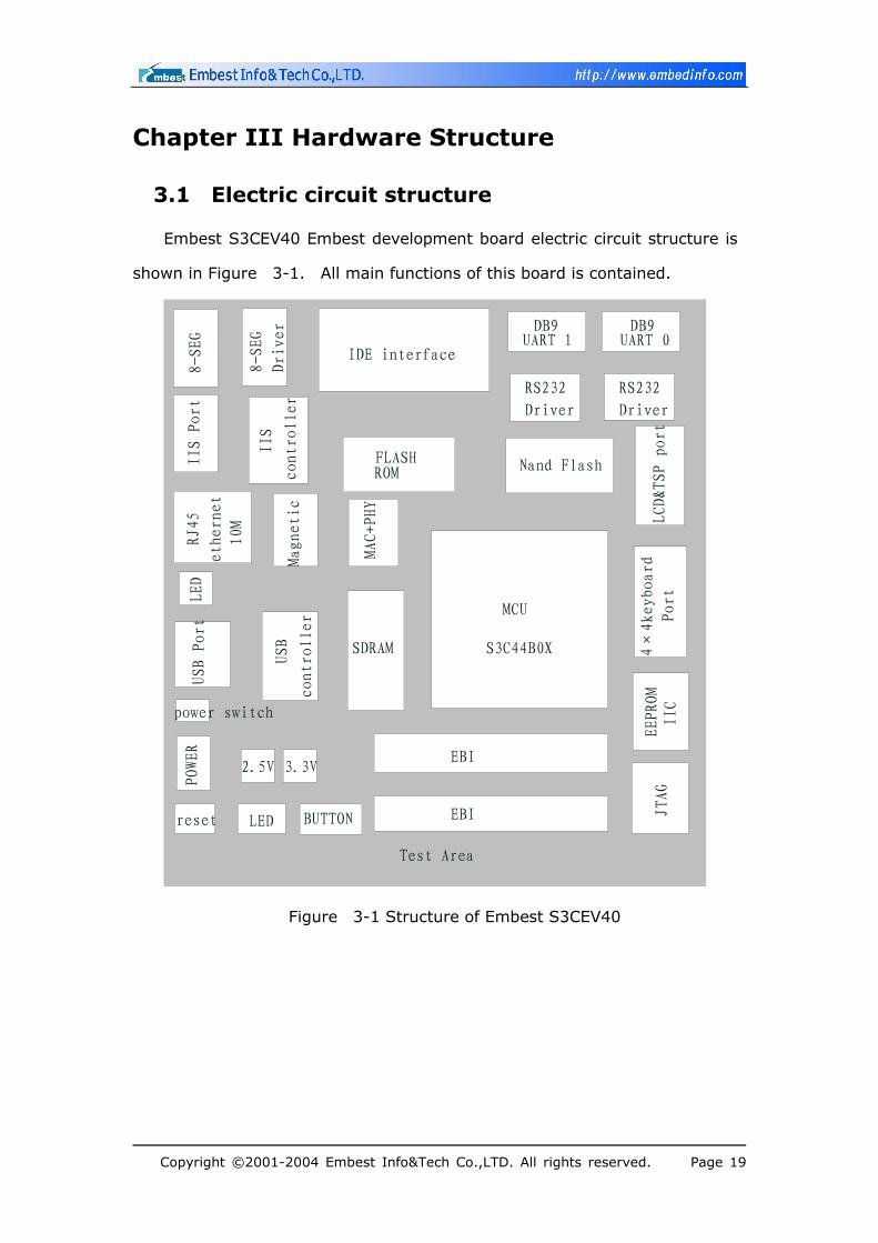
Chapter III Hardware Structure
3.1 Electric circuit structure
Embest S3CEV40 Embest development board electric circuit structure is
shown in Figure 3-1. All main functions of this board is contained.
SDRAM
FLASH Nand FlashROM
S3C44B0X
MCU
IIC
JTAG
USB Port
IDE interface
LCD&TSP port
4×
4keyboard
10M
RJ45
8-SEG
DB9
IIS Port
RS232
Driver
IIS
8-SEG
Driver
USB
Magnetic
MAC+PHY
LED
POWER
3.3V2.5V
controller
ethernet
Port
UART 1
controller
EEPROM
DB9
RS232
Driver
UART 0
power switch
reset LED BUTTON
EBI
EBI
Test Area
Figure 3-1 Structure of Embest S3CEV40
Copyright ©2001-2004 Embest Info&Tech Co.,LTD. All rights reserved. Page 19
Page 20
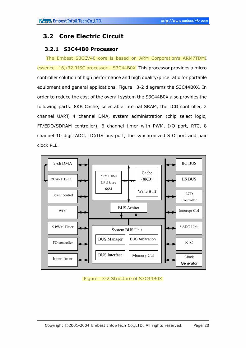
3.2 Core Electric Circuit
3.2.1 S3C44B0 Processor
The Embest S3CEV40 core is based on ARM Corporation’s ARM7TDMI
essence--16,/32 RISC processor --S3C44B0X. This processor provides a micro
controller solution of high performance and high quality/price ratio for portable
equipment and general applications. Figure 3-2 diagrams the S3C44B0X. In
order to reduce the cost of the overall system the S3C44B0X also provides the
following parts: 8KB Cache, selectable internal SRAM, the LCD controller, 2
channel UART, 4 channel DMA, system administration (chip select logic,
FP/EDO/SDRAM controller), 6 channel timer with PWM, I/O port, RTC, 8
channel 10 digit ADC, IIC/IIS bus port, the synchronized SIO port and pair
clock PLL.
2-ch DMA
2UART 1SIO
Inner Timer
Power control
WDT
5 PWM Timer
I/O controller
8 ADC 10bit
Interrupt Ctrl
LCD
Controller
IIS BUS
Clock
Generator
IIC BUS
RTC
BUS Arbiter
System BUS Unit
Memory CtrlBUS Interface
BUS ArbitrationBUS Manager
ARM7TDMI
CPU Core
66M
Cache(8KB)
Write Buff
Figure 3-2 Structure of S3C44B0X
Copyright ©2001-2004 Embest Info&Tech Co.,LTD. All rights reserved. Page 20
Page 21
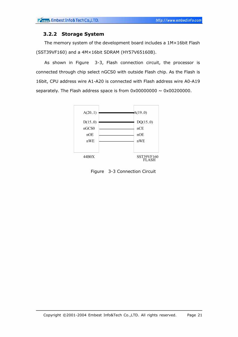
3.2.2 Storage System
The memory system of the development board includes a 1M×16bit Flash
(SST39VF160) and a 4M×16bit SDRAM (HY57V65160B).
As shown in Figure 3-3, Flash connection circuit, the processor is
connected through chip select nGCS0 with outside Flash chip. As the Flash is
16bit, CPU address wire A1-A20 is connected with Flash address wire A0-A19
separately. The Flash address space is from 0x00000000 ~ 0x00200000.
44B0X SST39VF160FLASH
A(20..1) A(19..0)
DQ(15..0)D(15..0)nGCS0
nOEnWE
nCEnOEnWE
Figure 3-3 Connection Circuit
Copyright ©2001-2004 Embest Info&Tech Co.,LTD. All rights reserved. Page 21
Page 22
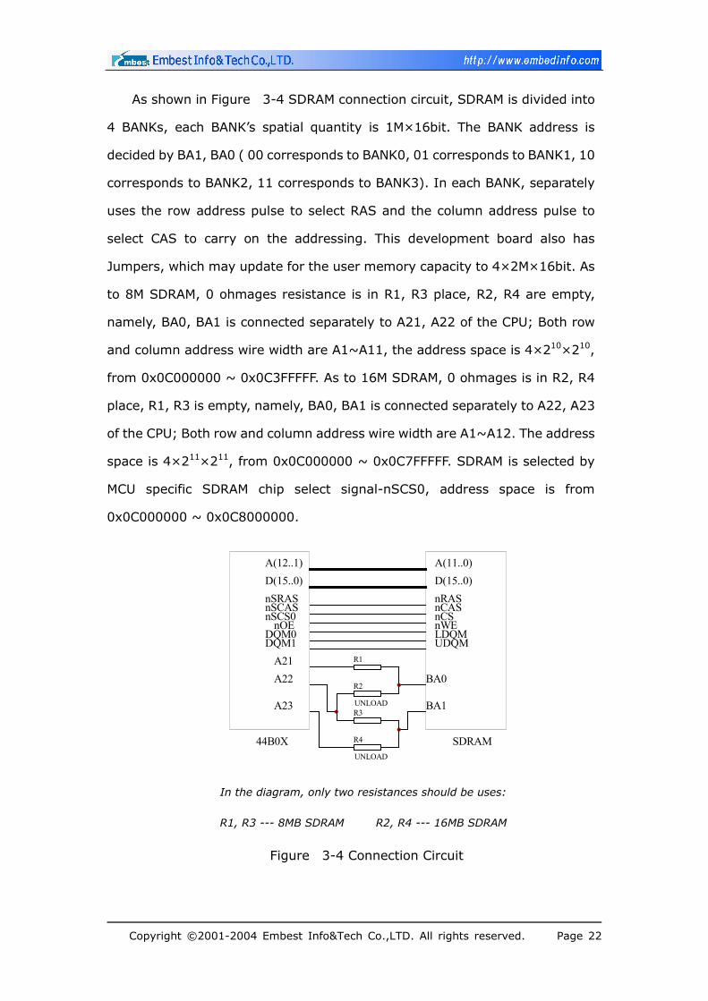
As shown in Figure 3-4 SDRAM connection circuit, SDRAM is divided into
4 BANKs, each BANK’s spatial quantity is 1M×16bit. The BANK address is
decided by BA1, BA0 ( 00 corresponds to BANK0, 01 corresponds to BANK1, 10
corresponds to BANK2, 11 corresponds to BANK3). In each BANK, separately
uses the row address pulse to select RAS and the column address pulse to
select CAS to carry on the addressing. This development board also has
Jumpers, which may update for the user memory capacity to 4×2M×16bit. As
to 8M SDRAM, 0 ohmages resistance is in R1, R3 place, R2, R4 are empty,
namely, BA0, BA1 is connected separately to A21, A22 of the CPU; Both row
and column address wire width are A1~A11, the address space is 4×210×210,
from 0x0C000000 ~ 0x0C3FFFFF. As to 16M SDRAM, 0 ohmages is in R2, R4
place, R1, R3 is empty, namely, BA0, BA1 is connected separately to A22, A23
of the CPU; Both row and column address wire width are A1~A12. The address
space is 4×211×211, from 0x0C000000 ~ 0x0C7FFFFF. SDRAM is selected by
MCU specific SDRAM chip select signal-nSCS0, address space is from
0x0C000000 ~ 0x0C8000000.
R1
R2
R3
R4
A(12..1)D(15..0) D(15..0)
A(11..0)
nSRASnCASnSCASnRASnCSnWELDQMUDQM
nSCS0nOE
DQM0DQM1
A21A22
A23
BA0
BA1
44B0X SDRAM
UNLOAD
UNLOAD
In the diagram, only two resistances should be uses:
R1, R3 --- 8MB SDRAM R2, R4 --- 16MB SDRAM
Figure 3-4 Connection Circuit
Copyright ©2001-2004 Embest Info&Tech Co.,LTD. All rights reserved. Page 22
Page 23
3.2.3 IIC EEPROM Interface
The development board has an EEPROM (AT24C040), whose capacity was
4Kbit, to support IIC bus. IIC is a bidirectional double-wire serial bus which is
used in the internal IC control. In standard mode, data transmission speed
may achieve 100kbit/s; In fast mode, 400kbit/s.
3.2.4 Power Supply, Reset, Clock Circuit and JTAG Port
This development board is powered by DC 5V regulated power supply.
After the electricity is inputed, two constant voltages chips on the board
separately produces 3.3V and 2.5V voltage for MCU I/O and ARM core;
There is a RESET button on the development board. You may press down
this button to reset the system;
The real-time clock is realized by connecting MCU to an external
32.768KHz crystal oscillator;
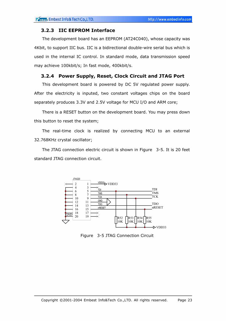
The JTAG connection electric circuit is shown in Figure 3-5. It is 20 feet
standard JTAG connection circuit.
2468101214
13579
1113151617181920
JTAG20VDD33
TDITMSTCKGNDTDOnRESET
VDD33
VDD33
TDITMSTCK
TDOnRESET
GNDR5310K
R5210K
R5410K
R5510K
Figure 3-5 JTAG Connection Circuit
Copyright ©2001-2004 Embest Info&Tech Co.,LTD. All rights reserved. Page 23
Page 24
3.2.5 Switch and State Indicating LED
SW1 is the power switch of the entire development board. When the switch
is in the position of "USBPOWER", the development board is powered by USB;
When the switch is in the position of "EXTPOWER", by external power supply.
D3 is the power indicating lamp, which may indicate if board is with
electricity.
Moreover, the ethernet port also has 4 status indicating lamps, which are:
D5-connection indicating lamp;
D6- data receiving indicating lamp;
D13- data transmitting indicating lamp;
D14-Auto-testing passed indicating lamp.
Copyright ©2001-2004 Embest Info&Tech Co.,LTD. All rights reserved. Page 24
Page 25
3.3 Embest S3CEV40 Communication Port Circuit
3.3.1 Serial Port
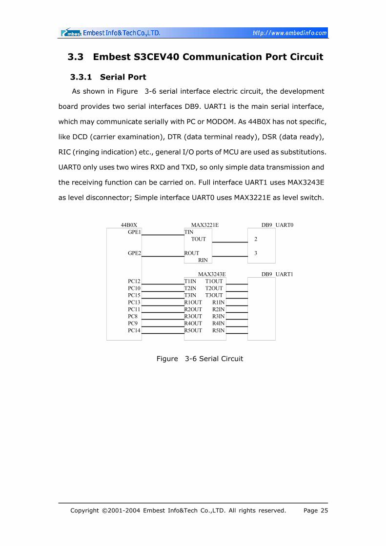
As shown in Figure 3-6 serial interface electric circuit, the development
board provides two serial interfaces DB9. UART1 is the main serial interface,
which may communicate serially with PC or MODOM. As 44B0X has not specific,
like DCD (carrier examination), DTR (data terminal ready), DSR (data ready),
RIC (ringing indication) etc., general I/O ports of MCU are used as substitutions.
UART0 only uses two wires RXD and TXD, so only simple data transmission and
the receiving function can be carried on. Full interface UART1 uses MAX3243E
as level disconnector; Simple interface UART0 uses MAX3221E as level switch.
TIN
ROUT
TOUT
RIN
2
3
T1INT2INT3IN
T1OUTT2OUTT3OUT
R1OUTR2OUTR3OUTR4OUTR5OUT
R1INR2INR3INR4INR5IN
PC8PC9
PC10
PC11
PC12
PC13
PC14
PC15
GPE1
GPE2
DB9
DB9
UART0
UART1
MAX3221E
MAX3243E
44B0X
Figure 3-6 Serial Circuit
Copyright ©2001-2004 Embest Info&Tech Co.,LTD. All rights reserved. Page 25
Page 26
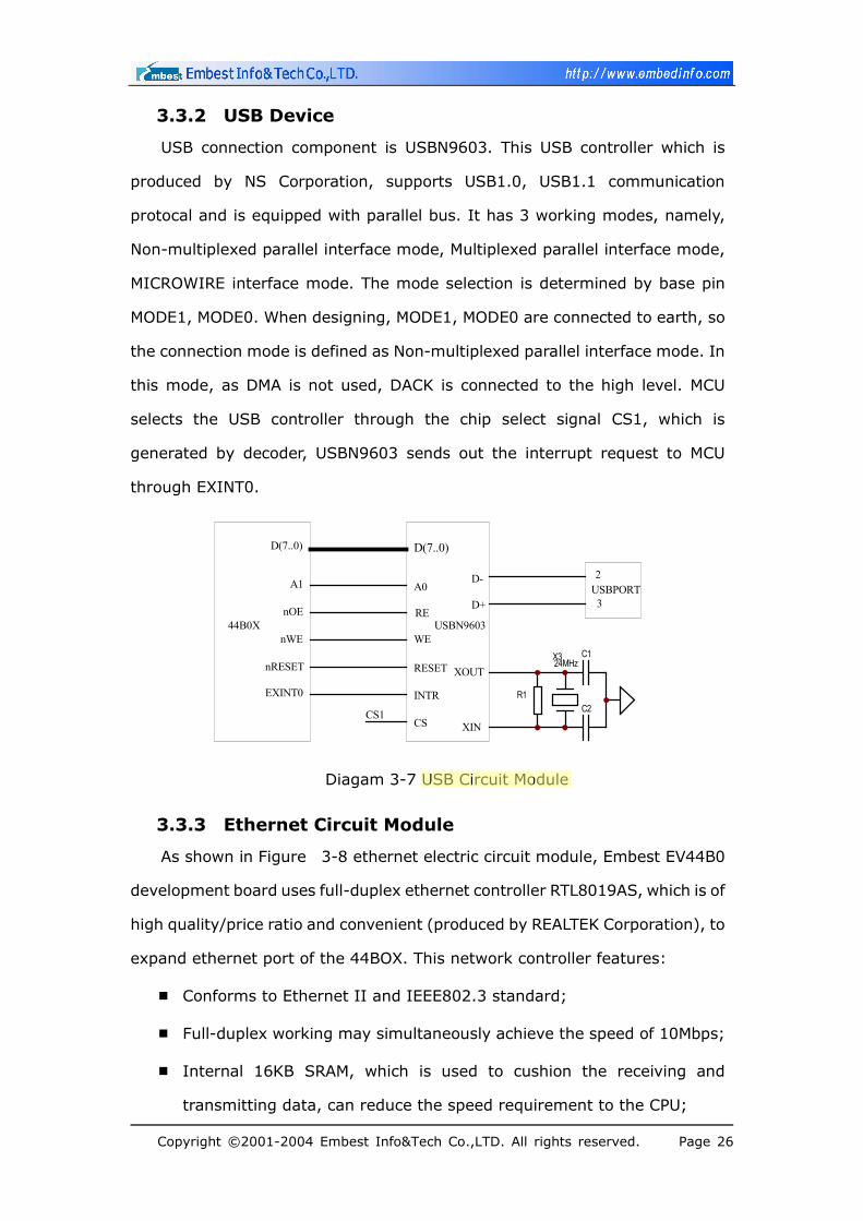
3.3.2 USB Device
USB connection component is USBN9603. This USB controller which is
produced by NS Corporation, supports USB1.0, USB1.1 communication
protocal and is equipped with parallel bus. It has 3 working modes, namely,
Non-multiplexed parallel interface mode, Multiplexed parallel interface mode,
MICROWIRE interface mode. The mode selection is determined by base pin
MODE1, MODE0. When designing, MODE1, MODE0 are connected to earth, so
the connection mode is defined as Non-multiplexed parallel interface mode. In
this mode, as DMA is not used, DACK is connected to the high level. MCU
selects the USB controller through the chip select signal CS1, which is
generated by decoder, USBN9603 sends out the interrupt request to MCU
through EXINT0.
D(7..0)
A1 A0
nOE
nWE
nRESET
EXINT0
CS1
RE
WE
RESET
INTR
CS
R1
X324MHz
C1
C2
XOUT
XIN
D-
D+
44B0X USBN9603
USBPORT2
3
D(7..0)
Diagam 3-7 USB Circuit Module
3.3.3 Ethernet Circuit Module
As shown in Figure 3-8 ethernet electric circuit module, Embest EV44B0
development board uses full-duplex ethernet controller RTL8019AS, which is of
high quality/price ratio and convenient (produced by REALTEK Corporation), to
expand ethernet port of the 44BOX. This network controller features:
Conforms to Ethernet II and IEEE802.3 standard;
Full-duplex working may simultaneously achieve the speed of 10Mbps;
Copyright ©2001-2004 Embest Info&Tech Co.,LTD. All rights reserved. Page 26
Internal 16KB SRAM, which is used to cushion the receiving and
transmitting data, can reduce the speed requirement to the CPU;
Page 27
Supports 8,/16 digit data bus, 8 interrupt request line, and 16 I/O base
address selection;
Supports UTP, AVI and BNC automatic detection, also supports
automatic polar revision to 10BaseT topology;
Permits 4 conclusion LED pin programmable output;
100 feet PQFP seal, which reduced the PCB board size.
RTL8019AS has three working modes. In Built-in mode application, if
93C46 is not used, the cost may be reduced, simultaneously the connections
are reduced. So usually Jumper mode is used. The net card I/O base address is
determined by IOS3, IOS2, IOS1 and IOS0. RTL8019AS integrated two RAM.
One is 16KB, whose address is 0x4000~0x7FFF; another is 32 bytes, whose
address is 0x0000~0x001F. RAM stores the data by page. Every 256 bytes
consists a page. Generally, page 0 is called PROM, which is to store net card
address. It is read out from 93C46 when the net card reset. But as this board
did not use 93C46, PROM cannot be used. So a program should be made to
assign a net card address and write into MAR0~MAR5. 16KB RAM serves as the
buffering area of receiving and transmitting data. Generally 0x4000~0x46FF
serves as buffering area for transmitting, 0x4700~0x7FFF serves as buffering
area for receiving.
D(15..0) SD(15..0)
A(12..8) SA(4..0)
IORBIOWBRSTRVnRESET
nWEnOE
EXINT3 INT0
A20
A18A19
nGCS1 S3A0A1A2
Y7 CS7 AEN
HDLD
TPIN+TPIN-
1364 7
91012 1
2
36
44BOX 74LV138 RTL8019AS
FB2022 RJ45
Figure 3-8 Ethernet Circuit Module
Copyright ©2001-2004 Embest Info&Tech Co.,LTD. All rights reserved. Page 27
Page 28
3.4 External Expanded Module
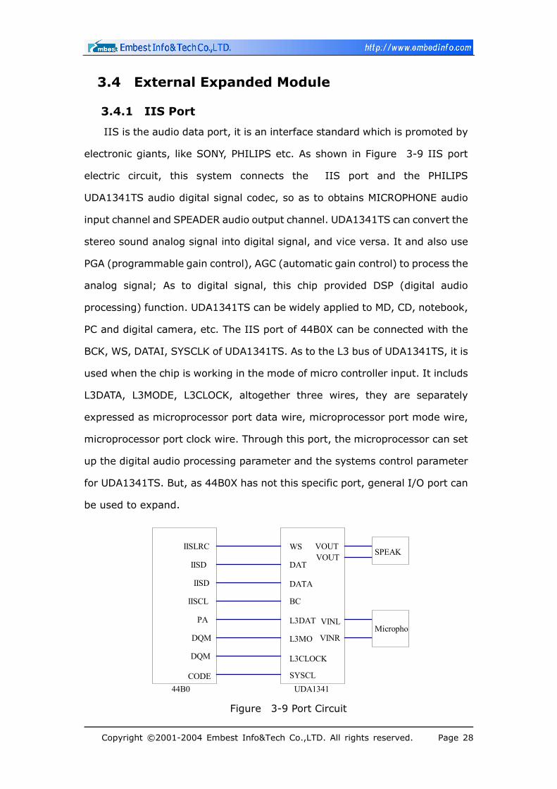
3.4.1 IIS Port
IIS is the audio data port, it is an interface standard which is promoted by
electronic giants, like SONY, PHILIPS etc. As shown in Figure 3-9 IIS port
electric circuit, this system connects the IIS port and the PHILIPS
UDA1341TS audio digital signal codec, so as to obtains MICROPHONE audio
input channel and SPEADER audio output channel. UDA1341TS can convert the
stereo sound analog signal into digital signal, and vice versa. It and also use
PGA (programmable gain control), AGC (automatic gain control) to process the
analog signal; As to digital signal, this chip provided DSP (digital audio
processing) function. UDA1341TS can be widely applied to MD, CD, notebook,
PC and digital camera, etc. The IIS port of 44B0X can be connected with the
BCK, WS, DATAI, SYSCLK of UDA1341TS. As to the L3 bus of UDA1341TS, it is
used when the chip is working in the mode of micro controller input. It includs
L3DATA, L3MODE, L3CLOCK, altogether three wires, they are separately
expressed as microprocessor port data wire, microprocessor port mode wire,
microprocessor port clock wire. Through this port, the microprocessor can set
up the digital audio processing parameter and the systems control parameter
for UDA1341TS. But, as 44B0X has not this specific port, general I/O port can
be used to expand.
PA
DQM
DQM
CODE
IISLRC
IISD
IISD
IISCL
WS
DATA
DAT
BC
L3MO
L3CLOCK
SYSCL
L3DAT VINL
VINR
VOUTVOUT
SPEAK
Micropho
44B0 UDA1341
Figure 3-9 Port Circuit
Copyright ©2001-2004 Embest Info&Tech Co.,LTD. All rights reserved. Page 28
Page 29
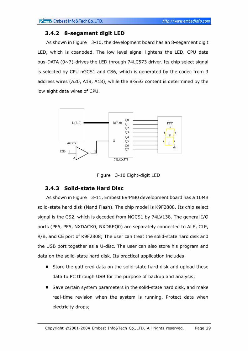
3.4.2 8-segament digit LED
As shown in Figure 3-10, the development board has an 8-segament digit
LED, which is coanoded. The low level signal lightens the LED. CPU data
bus-DATA (0~7)-drives the LED through 74LC573 driver. Its chip select signal
is selected by CPU nGCS1 and CS6, which is generated by the codec from 3
address wires (A20, A19, A18), while the 8-SEG content is determined by the
low eight data wires of CPU.
a
bf
c
g
de
DPY
dp
Q0Q1Q2Q3Q4Q5Q6Q71 2
A
CS6
D(7..0) D(7..0)
G44B0X
74LCX573
Figure 3-10 Eight-digit LED
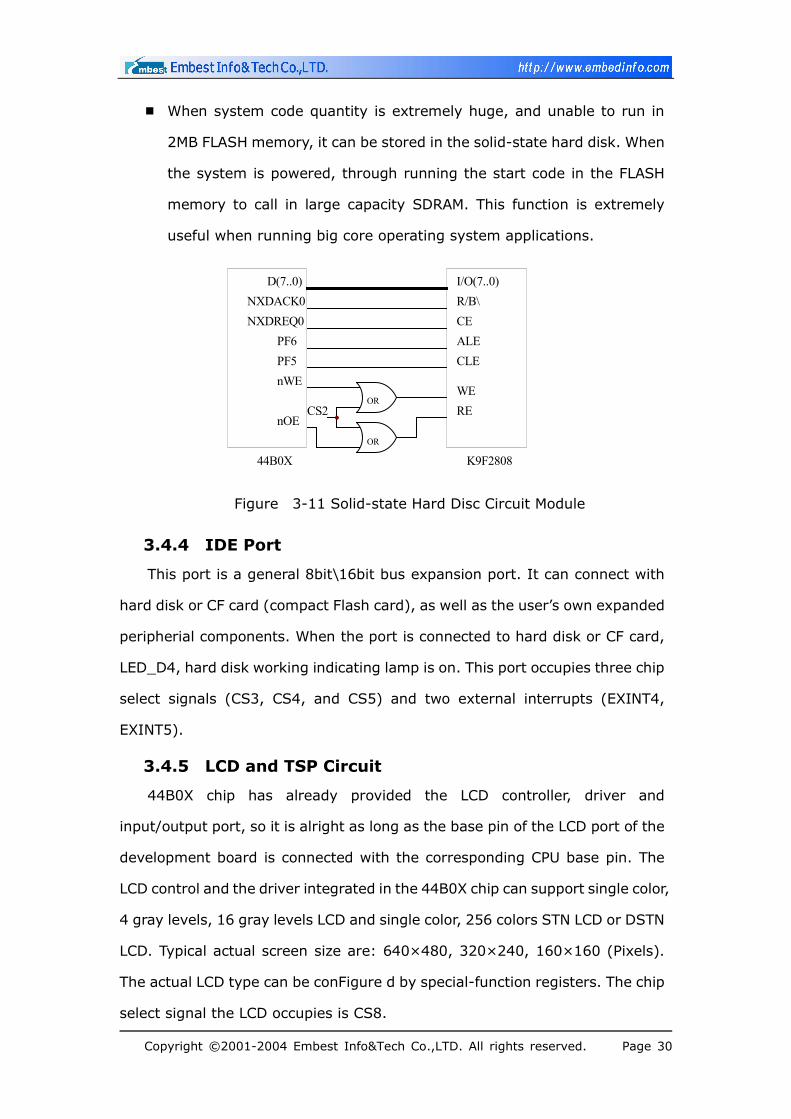
3.4.3 Solid-state Hard Disc
As shown in Figure 3-11, Embest EV44B0 development board has a 16MB
solid-state hard disk (Nand Flash). The chip model is K9F2808. Its chip select
signal is the CS2, which is decoded from NGCS1 by 74LV138. The general I/O
ports (PF6, PF5, NXDACK0, NXDREQ0) are separately connected to ALE, CLE,
R/B, and CE port of K9F2808; The user can treat the solid-state hard disk and
the USB port together as a U-disc. The user can also store his program and
data on the solid-state hard disk. Its practical application includes:
Store the gathered data on the solid-state hard disk and upload these
data to PC through USB for the purpose of backup and analysis;
Save certain system parameters in the solid-state hard disk, and make
real-time revision when the system is running. Protect data when
electricity drops;
Copyright ©2001-2004 Embest Info&Tech Co.,LTD. All rights reserved. Page 29
Page 30
When system code quantity is extremely huge, and unable to run in
2MB FLASH memory, it can be stored in the solid-state hard disk. When
the system is powered, through running the start code in the FLASH
memory to call in large capacity SDRAM. This function is extremely
useful when running big core operating system applications.
OR
OR
D(7..0) I/O(7..0)
ALE
R/B\CE
CLE
WERE
NXDACK0NXDREQ0
PF6PF5nWE
nOECS2
44B0X K9F2808
Figure 3-11 Solid-state Hard Disc Circuit Module
3.4.4 IDE Port
This port is a general 8bit\16bit bus expansion port. It can connect with
hard disk or CF card (compact Flash card), as well as the user’s own expanded
peripherial components. When the port is connected to hard disk or CF card,
LED_D4, hard disk working indicating lamp is on. This port occupies three chip
select signals (CS3, CS4, and CS5) and two external interrupts (EXINT4,
EXINT5).
3.4.5 LCD and TSP Circuit
Copyright ©2001-2004 Embest Info&Tech Co.,LTD. All rights reserved. Page 30
44B0X chip has already provided the LCD controller, driver and
input/output port, so it is alright as long as the base pin of the LCD port of the
development board is connected with the corresponding CPU base pin. The
LCD control and the driver integrated in the 44B0X chip can support single color,
4 gray levels, 16 gray levels LCD and single color, 256 colors STN LCD or DSTN
LCD. Typical actual screen size are: 640×480, 320×240, 160×160 (Pixels).
The actual LCD type can be conFigure d by special-function registers. The chip
select signal the LCD occupies is CS8.
Page 31
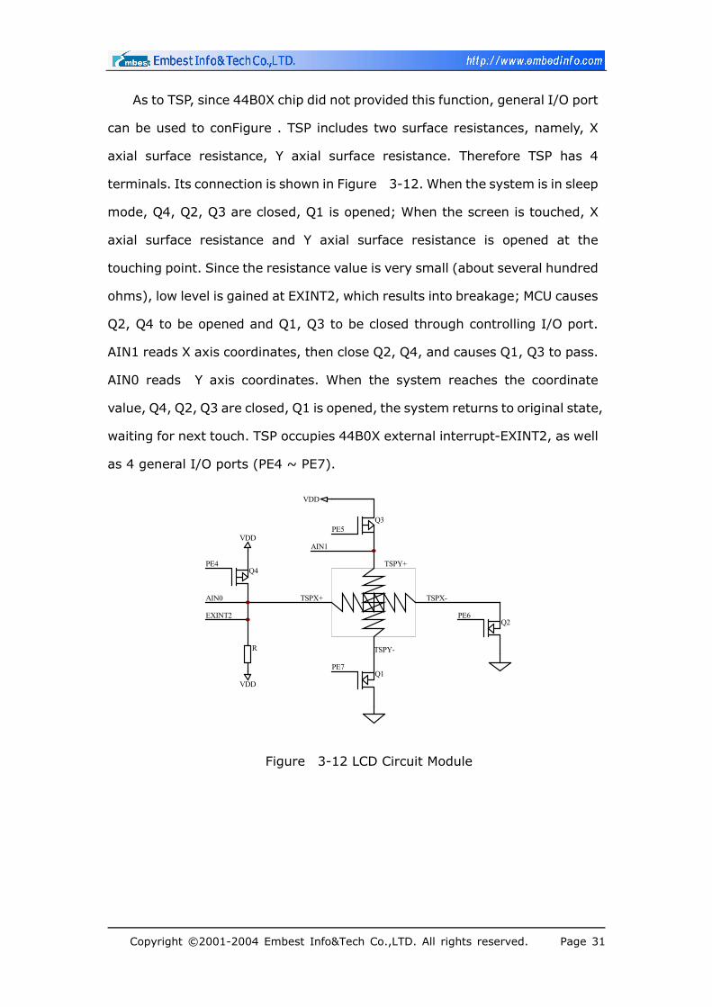
As to TSP, since 44B0X chip did not provided this function, general I/O port
can be used to conFigure . TSP includes two surface resistances, namely, X
axial surface resistance, Y axial surface resistance. Therefore TSP has 4
terminals. Its connection is shown in Figure 3-12. When the system is in sleep
mode, Q4, Q2, Q3 are closed, Q1 is opened; When the screen is touched, X
axial surface resistance and Y axial surface resistance is opened at the
touching point. Since the resistance value is very small (about several hundred
ohms), low level is gained at EXINT2, which results into breakage; MCU causes
Q2, Q4 to be opened and Q1, Q3 to be closed through controlling I/O port.
AIN1 reads X axis coordinates, then close Q2, Q4, and causes Q1, Q3 to pass.
AIN0 reads Y axis coordinates. When the system reaches the coordinate
value, Q4, Q2, Q3 are closed, Q1 is opened, the system returns to original state,
waiting for next touch. TSP occupies 44B0X external interrupt-EXINT2, as well
as 4 general I/O ports (PE4 ~ PE7).
Q3
Q4
Q2
Q1
R
VDD
AIN0
AIN1
EXINT2
PE4
PE5
PE7
PE6
VDD
VDD
TSPY+
TSPY-
TSPX-TSPX+
Figure 3-12 LCD Circuit Module
Copyright ©2001-2004 Embest Info&Tech Co.,LTD. All rights reserved. Page 31
Page 32
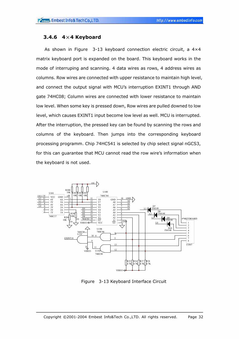
3.4.6 4×4 Keyboard
As shown in Figure 3-13 keyboard connection electric circuit, a 4×4
matrix keyboard port is expanded on the board. This keyboard works in the
mode of interruping and scanning. 4 data wires as rows, 4 address wires as
columns. Row wires are connected with upper resistance to maintain high level,
and connect the output signal with MCU’s interruption EXINT1 through AND
gate 74HC08; Column wires are connected with lower resistance to maintain
low level. When some key is pressed down, Row wires are pulled downed to low
level, which causes EXINT1 input become low level as well. MCU is interrupted.
After the interruption, the pressed key can be found by scanning the rows and
columns of the keyboard. Then jumps into the corresponding keyboard
processing programm. Chip 74HC541 is selected by chip select signal nGCS3,
for this can guarantee that MCU cannot read the row wire’s information when
the keyboard is not used.
12345678
4*4KEYBOARD
CON7
VDD33
12
1311U13D74HC08
9
108
714
U13C74HC08 4
56
U13B74HC08
VDD33
L0
L1
L2
L3
EXINT1
R354.7K
R364.7K
R374.7K
R384.7K
D71N4148
D81N4148
D91N4148
D101N4148
G1 1A1 2A2 3A3 4Y217
Y118
G219
VCC20
A4 5A5 6A6 7A7 8Y613
Y514
Y415
Y316
A8 9GND 10Y811
Y712
U100
74HC541
VDD33
D0D1D2D3 A1
A2A3A4
L0L1L2L3
NGCS3GND
GND
1A 11Y2 2A 32Y4
5A 116Y12 6A 13VCC14
3A 53Y6
GND 7
4Y8 4A 95Y10
U101
74HC17
R20010K R201
10KR202
10KR203
10K
R20410K
R20510K
GND
GND
VDD33
GND
GND
Figure 3-13 Keyboard Interface Circuit
Copyright ©2001-2004 Embest Info&Tech Co.,LTD. All rights reserved. Page 32
Page 33
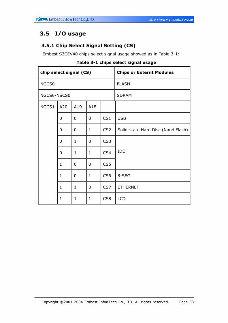
3.5 I/O usage
3.5.1 Chip Select Signal Setting (CS)
Embest S3CEV40 chips select signal usage showed as in Table 3-1:
Table 3-1 chips select signal usage
chip select signal (CS) Chips or Externt Modules
NGCS0 FLASH
NGCS6/NSCS0 SDRAM
A20 A19 A18
0 0 0 CS1 USB
0 0 1 CS2 Solid-state Hard Disc (Nand Flash)
0 1 0 CS3
0 1 1 CS4
1 0 0 CS5
IDE
1 0 1 CS6 8-SEG
1 1 0 CS7 ETHERNET
NGCS1
1 1 1 CS8 LCD
Copyright ©2001-2004 Embest Info&Tech Co.,LTD. All rights reserved. Page 33
Page 34
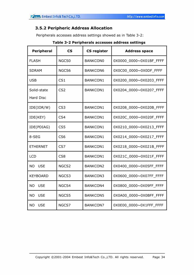
3.5.2 Peripheric Address Allocation
Peripherals accesses address settings showed as in Table 3-2:
Table 3-2 Peripherals accesses address settings
Peripheral CS CS register Address space
FLASH NGCS0 BANKCON0 0X0000_0000~0X01BF_FFFF
SDRAM NGCS6 BANKCON6 0X0C00_0000~0X0DF_FFFF
USB CS1 BANKCON1 0X0200_0000~0X0203_FFFF
Solid-state
Hard Disc
CS2 BANKCON1 0X0204_0000~0X0207_FFFF
IDE(IOR/W) CS3 BANKCON1 0X0208_0000~0X020B_FFFF
IDE(KEY) CS4 BANKCON1 0X020C_0000~0X020F_FFFF
IDE(PDIAG) CS5 BANKCON1 0X0210_0000~0X0213_FFFF
8-SEG CS6 BANKCON1 0X0214_0000~0X0217_FFFF
ETHERNET CS7 BANKCON1 0X0218_0000~0X021B_FFFF
LCD CS8 BANKCON1 0X021C_0000~0X021F_FFFF
NO USE NGCS2 BANKCON2 0X0400_0000~0X05FF_FFFF
KEYBOARD NGCS3 BANKCON3 0X0600_0000~0X07FF_FFFF
NO USE NGCS4 BANKCON4 0X0800_0000~0X09FF_FFFF
NO USE NGCS5 BANKCON5 0X0A00_0000~0X0BFF_FFFF
NO USE NGCS7 BANKCON7 0X0E00_0000~0X1FFF_FFFF
Copyright ©2001-2004 Embest Info&Tech Co.,LTD. All rights reserved. Page 34
Page 35
3.5.3 I/O ports Table 3-3 Port A
Port A Pin function Port A Pin function Port A Pin function
PA0 ADDR0 PA4 ADDR19 PA8 ADDR23
PA1 ADDR16 PA5 ADDR20 PA9 OUTPUT(IIS)
PA2 ADDR17 PA6 ADDR21
PA3 ADDR18 PA7 ADDR22
PCONA access address: 0X01D20000
PDATA access address: 0X01D20004
PCONA reset value: 0X1FF
Table 3-4 Port B
Port B Pin function Port B Pin function Port B Pin function
PB0 SCKE PB4 OUTPUT(IIS) PB8 NGCS3
PB1 SCLE PB5 OUTPUT(IIS) PB9 OUTPUT(LED1)
PB2 nSCAS PB6 nGCS1 PB10 OUTPUT(LED2)
PB3 nSRAS PB7 NGCS2
PCONB access address: 0X01D20008
PDATB access address: 0X01D2000C
PCONB reset value: 0X7FF
Table 3-5 Port C
Port C Pin function Port C Pin function Port C Pin function
PC0 IISLRCK PC6 VD5 PC12 TXD1
PC1 IISDO PC7 VD4 PC13 RXD1
PC2 IISDI PC8 INPUT(UART) PC14 INPUT(UART)
PC3 IISCLK PC9 INPUT(UART) PC15 INPUT(UART)
Copyright ©2001-2004 Embest Info&Tech Co.,LTD. All rights reserved. Page 35
Page 36
PC4 VD7 PC10 RTS1
PC5 VD6 PC11 CTS1
PCONC access address: 0X01D20010
PDATC access address: 0X01D20014
PUPC access address: 0X01D20018
PCONC reset value: 0X0FF0FFFF
Table 3-6 Port D
Port D Pin function Port D Pin function Port D Pin function
PD0 VD0 PD3 VD3 PD6 VM
PD1 VD1 PD4 VCLK PD7 VFRAME
PD2 VD2 PD5 VLINE
PCOND access address: 0X01D2001C
PDATD access address: 0X01D20020
PUPD access address: 0X01D20024
PCOND reset value: 0XAAAA
Table 3-7 Port E
Port E Pin function Port E Pin function Port E Pin function
PE0 OUTPUT(LCD) PE3 RESERVE PE6 OUTPUT(TSP)
PE1 TXD0 PE4 OUTPUT(TSP) PE7 OUTPUT(TSP)
PE2 RXD0 PE5 OUTPUT(TSP) PE8 CODECLK
PCONE access address: 0X01D20028
PDATE access address: 0X01D2002C
PUPE access address: 0X01D20030
PCONE reset value: 0X25529
Copyright ©2001-2004 Embest Info&Tech Co.,LTD. All rights reserved. Page 36
Page 37
Table 3-8 Port F
Port F Pin function Port F Pin function Port F Pin function
PF0 IICSCL PF3 IN(Nand Flash) PF6 out(Nand
Flash)
PF1 IICSDA PF4 out(Nand Flash) PF7 IN(bootloader)
PF2 RESERVED PF5 out(Nand Flash) PF8 IN(bootloader)
PCONF access address: 0X01D20034
PDATF access address: 0X01D20038
PUPF access address: 0X01D2003C
PCONF reset value: 0X00252A
Table 3-9 Port G
Port G Pin function Port G Pin function Port G Pin function
PG0 EXINT0 PG3 EXINT3 PG6 EXINT6
PG1 EXINT1 PG4 EXINT4 PG7 EXINT7
PG2 EXINT2 PG5 EXINT5
PCONG access address: 0X01D20040
PDATG access address: 0X01D20044
PUPG access address: 0X01D20048
PCONG reset value: 0XFFFF
3.6 Bus Expansion
Embest EV44B0 development board has reserved the expanded ports for
all pins and the user can conveniently expand memory and other external
equipments according to his own need. It can satisfy the application of most
products. The user needs to make his own expanding board when expanding,
so long as the definition of the expanding board port is corresponded to the
expanded port in the development board.
Copyright ©2001-2004 Embest Info&Tech Co.,LTD. All rights reserved. Page 37
Page 38
Chapter IV Software System
4.1.1 Software Development
The development board provides abundant operating routine programs so
that user can carry out quick software development on certain products. User
can use any example routine program as software development template and
can thereby write software programs according to actual hardware
environment to shorten development cycle greatly.
While developing softwares, user shall pay attention to:
1) If the software is being debugged in RAM, the configuration of memory
area is to be completed by integrated environment via script command files.
Therefore, there is no need to use configuration code of memory area in
program.
2) When debugging in RAM, the content of data field can be selected
automatically by judging if the addresses of read only area and read – and –
write area overlap, therefore the content of data field does not need to be
copied.
3) If failing to profetch abnormal vectors in code and not processed, a
complete program should process any abnormal vector including saving for
query the execution state before entering into abnormal vector. Return back to
program to resume execution after clearing the possible errors caused by
abnormal vectors.
Copyright ©2001-2004 Embest Info&Tech Co.,LTD. All rights reserved. Page 38
Page 39
4.1.2 Software Debugging
RAM Debugging
Embest IDE for ARM provides users with two debugging methods: RAM
debugging and Flash debugging. Because the ARM area is very easy to
read and write, and the access speed is very fast, all users’ program debugging
during the process of software development should be completed in RAM area
as long as hardware permits. Flexible uses of RAM debugging and Flash
debugging can quickly find and process many complex program problems
during the process of project development to accelerate the project
development progress.
The following steps should be completed before carrying out software
debugging under Embest IDE for ARM development environment: compiling
linking project, connecting emulator & circuit board and downloading program.
Compiling and Linking Project
Users can select Build menu to compile corresponding file or project.
Output corresponding compiling and linking information in Build sub-window of
Output window. Program compilation, according to linking configuration and
under project directory\debug\directory, will generate l.elf file which contains
execution file of debugging information.
Connecting Emulator and Development Board
Select Remote Connect sub-menu of Debug menu, the debugger in
integrated environment will connect target system through emulator.
Program download
Copyright ©2001-2004 Embest Info&Tech Co.,LTD. All rights reserved. Page 39
Page 40
After connecting target system, debugger will download software
automatically if the auto-download option has been set in debugging and
configuration option, otherwise select Download sub-menu of menu Debug to
download program, and then debugger will download binary instruction file to
memory area of target board after clearing debugging information in .elf file
and at the same time display download progress at the red status bar. The
download address is initial address of RAM memory area mapped by demand
script. “Download Completed” will be displayed in blue status bar or ‘Download
Failed’ will be displayed in red status bar after the download is finished.
Flash Debugging
The application program (Bin code), which has passed debugging in RAM,
can be burn-writen into Flash chip for debugging when the circuit is restricted
by hardware resource. For example, the space of RAM is smaller than program
code space and cannot be debugged in RAM, or it’s necessary to observe the
operating state of application program in actual hardware environment. Users
should carry out debugging work if the operation program, which is
burn-written to flash chip, cannot obtain correct result or observe the
operating state of the program in Flash.
The project configuration is different between debugging program in Flash
and debugging program in RAM.
It’s not necessary to execute script file in debugging option, it will be
completed in start file. It’s necessary to change Action after Connected
option to None;
Debugging process is also different:
Connect with emulator and need not to Download;
reset command should be executed before starting debugging program
from the entrance of start program, and the program will stay in zero-address;
Program can set at most two hardware breakpoints when debugging in
Flash.
Copyright ©2001-2004 Embest Info&Tech Co.,LTD. All rights reserved. Page 40
Page 41
4.1.3 Program onto Flash
There are differences between program passed debugging in RAM and
program solidified finally onto the circuit board of Flash, users need to:
Set compilation definition symbol at the Pre-define options of
assembler or add Define & Compile option directly at initial files, then
the repetitive mapping will be completed at storage area automatically
by start files instead of demand script.
Select flash.ld in linking files of linker, and then the transporting work
of data field downloaded into Flash initially will be completed by linking
files and start files.
Re-compile program after completing above alterations. Convert ‘.elf’
files to binary instruction format file (bin) by using ‘Elf to Bin’ tool, and
then use ‘Embest Flash Programmer’ tool to download ‘.bin’ into Flash
of circuit board.
Copyright ©2001-2004 Embest Info&Tech Co.,LTD. All rights reserved. Page 41
Page 42
4.2 Introduction to Start Program
Attention should be given when designing start program. The processor
S3C44B0 used by development board has no repetitive mapping function at
memory area and all address of memory area is fixed, and in addition S3C44B0
provides vector interruption function to reduce interruption delay. Therefore
vector interruption function can expand the vector table, assist program
designing & debugging in RAM and the interrupting entrance transfers to the
top area of RAM through address defining.
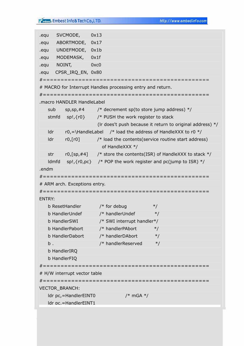
The following codes are source codes and explanation of S3C44B0 start
program. Partial similar definitions of interruption entrances and Macro has
been replace by ‘……’ with notes. Users can modify or self-add the program of
omitted part by referring to relevant data manual if the users want to use the
following source codes as start program.
Copyright ©2001-2004 Embest Info&Tech Co.,LTD. All rights reserved. Page 42
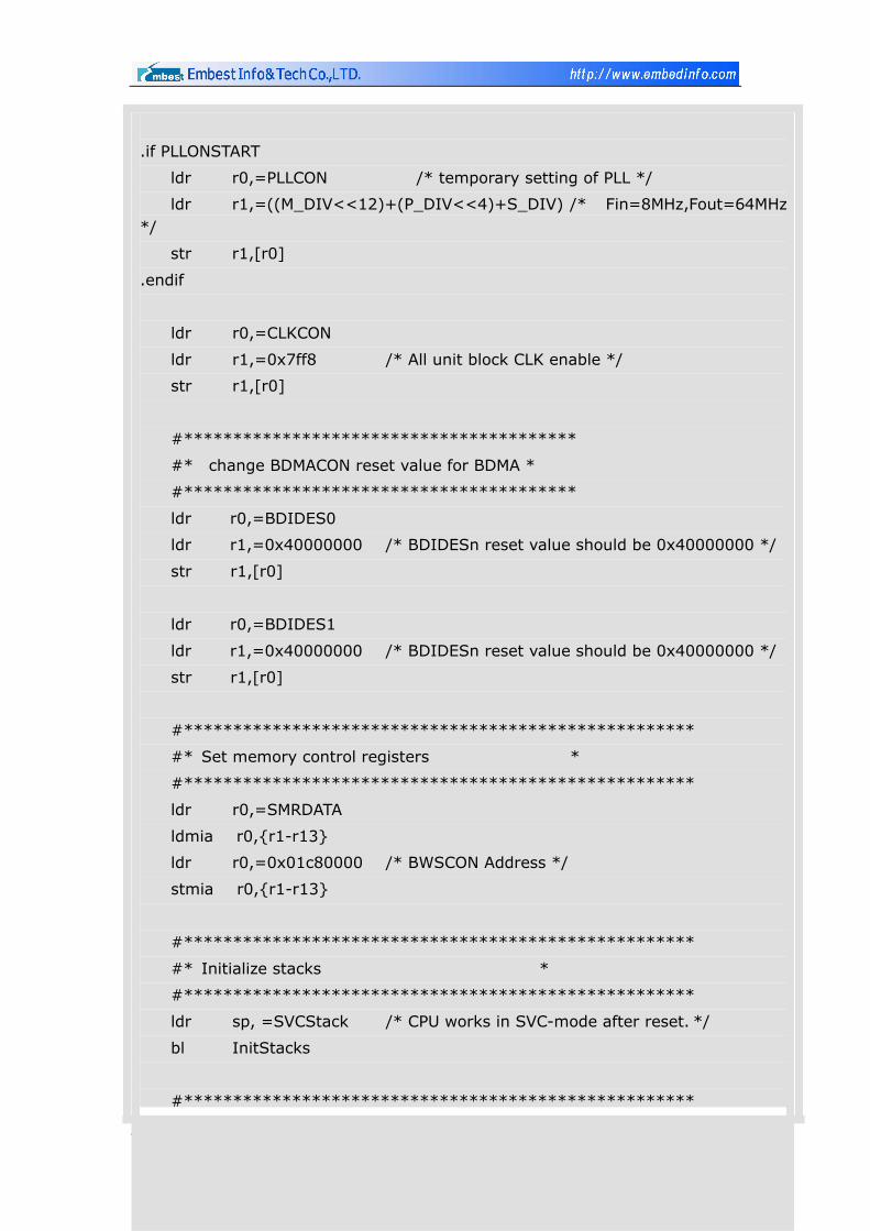
# *******************************************************
# * NAME : 44BINIT.S *
# * Version : 10.April.2000 *
# * Description: *
# * C start up codes *
# * ConFigure memory, Initialize ISR ,stacks *
# * Initialize C-variables *
# * Fill zeros into zero-initialized C-variables *
# *******************************************************
#===============================================
# Registers and symbol definitions
#===============================================
.equ INTMSK, 0x01e0000c
.equ WTCON, 0x01d30000
.equ CLKCON, 0x01d80004
.equ LOCKTIME, 0x01d8000c
.equ FIQMODE, 0x11
.equ IRQMODE, 0x12
Page 43
Copyright ©2001-2004 Embest Info&Tech Co.,LTD. All rights reserved. Page 43
.equ SVCMODE, 0x13
.equ ABORTMODE, 0x17
.equ UNDEFMODE, 0x1b
.equ MODEMASK, 0x1f
.equ NOINT, 0xc0
.equ CPSR_IRQ_EN, 0x80
#===============================================
# MACRO for Interrupt Handles processing entry and return.
#===============================================
.macro HANDLER HandleLabel
sub sp,sp,#4 /* decrement sp(to store jump address) */
stmfd sp!,{r0} /* PUSH the work register to stack
(lr does't push because it return to original address) */
ldr r0,=\HandleLabel /* load the address of HandleXXX to r0 */
ldr r0,[r0] /* load the contents(service routine start address)
of HandleXXX */
str r0,[sp,#4] /* store the contents(ISR) of HandleXXX to stack */
ldmfd sp!,{r0,pc} /* POP the work register and pc(jump to ISR) */
.endm
#===============================================
# ARM arch. Exceptions entry.
#===============================================
ENTRY:
b ResetHandler /* for debug */
b HandlerUndef /* handlerUndef */
b HandlerSWI /* SWI interrupt handler*/
b HandlerPabort /* handlerPAbort */
b HandlerDabort /* handlerDAbort */
b . /* handlerReserved */
b HandlerIRQ
b HandlerFIQ
#===============================================
# H/W interrupt vector table
#===============================================
VECTOR_BRANCH:
ldr pc,=HandlerEINT0 /* mGA */
ldr pc,=HandlerEINT1
Page 44
Copyright ©2001-2004 Embest Info&Tech Co.,LTD. All rights reserved. Page 44
…… @ Omit
ldr pc,=HandlerADC /* mGB */
…… @ Omit
b .
#===============================================
# Interrupt(s) handle after MACRO expanded
#===============================================
HandlerFIQ: HANDLER HandleFIQ
HandlerIRQ: HANDLER HandleIRQ
HandlerUndef: HANDLER HandleUndef
HandlerSWI: HANDLER HandleSWI
HandlerDabort: HANDLER HandleDabort
HandlerPabort: HANDLER HandlePabort
HandlerADC: HANDLER HandleADC
…… @ Omit
HandlerEINT1: HANDLER HandleEINT1
HandlerEINT0: HANDLER HandleEINT0
#===============================================
# Reset exception entry point
#===============================================
ldr r0,=WTCON /* watch dog disable*/
ldr r1,=0x0
str r1,[r0]
ldr r0,=INTMSK
ldr r1,=0x07ffffff /* all interrupt disable */
str r1,[r0]
#****************************************************
#* Set clock control registers *
#****************************************************
ldr r0,=LOCKTIME
ldr r1,=0xfff
str r1,[r0]
Page 45
Copyright ©2001-2004 Embest Info&Tech Co.,LTD. All rights reserved. Page 45
.if PLLONSTART
ldr r0,=PLLCON /* temporary setting of PLL */
ldr r1,=((M_DIV<<12)+(P_DIV<<4)+S_DIV) /* Fin=8MHz,Fout=64MHz */
str r1,[r0]
.endif
ldr r0,=CLKCON
ldr r1,=0x7ff8 /* All unit block CLK enable */
str r1,[r0]
#****************************************
#* change BDMACON reset value for BDMA *
#****************************************
ldr r0,=BDIDES0
ldr r1,=0x40000000 /* BDIDESn reset value should be 0x40000000 */
str r1,[r0]
ldr r0,=BDIDES1
ldr r1,=0x40000000 /* BDIDESn reset value should be 0x40000000 */
str r1,[r0]
#****************************************************
#* Set memory control registers *
#****************************************************
ldr r0,=SMRDATA
ldmia r0,{r1-r13}
ldr r0,=0x01c80000 /* BWSCON Address */
stmia r0,{r1-r13}
#****************************************************
#* Initialize stacks *
#****************************************************
ldr sp, =SVCStack /* CPU works in SVC-mode after reset. */
bl InitStacks
#****************************************************
Page 46
Copyright ©2001-2004 Embest Info&Tech Co.,LTD. All rights reserved. Page 46
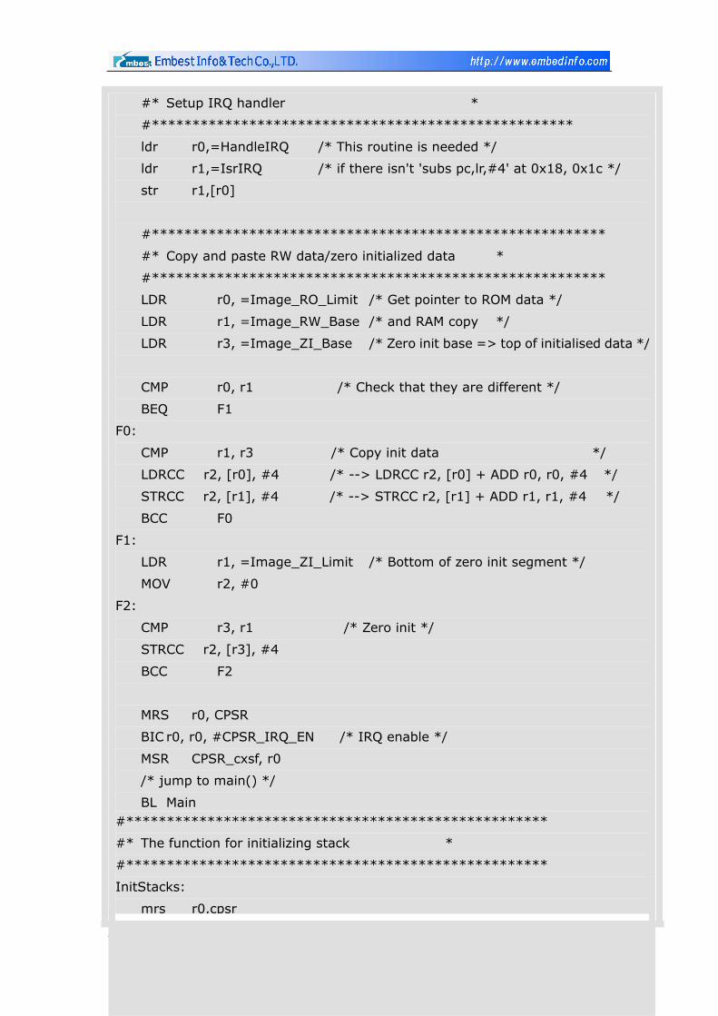
#* Setup IRQ handler *
#****************************************************
ldr r0,=HandleIRQ /* This routine is needed */
ldr r1,=IsrIRQ /* if there isn't 'subs pc,lr,#4' at 0x18, 0x1c */
str r1,[r0]
#********************************************************
#* Copy and paste RW data/zero initialized data *
#********************************************************
LDR r0, =Image_RO_Limit /* Get pointer to ROM data */
LDR r1, =Image_RW_Base /* and RAM copy */
LDR r3, =Image_ZI_Base /* Zero init base => top of initialised data */
CMP r0, r1 /* Check that they are different */
BEQ F1
F0:
CMP r1, r3 /* Copy init data */
LDRCC r2, [r0], #4 /* --> LDRCC r2, [r0] + ADD r0, r0, #4 */
STRCC r2, [r1], #4 /* --> STRCC r2, [r1] + ADD r1, r1, #4 */
BCC F0
F1:
LDR r1, =Image_ZI_Limit /* Bottom of zero init segment */
MOV r2, #0
F2:
CMP r3, r1 /* Zero init */
STRCC r2, [r3], #4
BCC F2
MRS r0, CPSR
BIC r0, r0, #CPSR_IRQ_EN /* IRQ enable */
MSR CPSR_cxsf, r0
/* jump to main() */
BL Main #****************************************************
#* The function for initializing stack *
#****************************************************
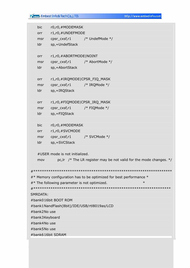
InitStacks:
mrs r0,cpsr
Page 47
Copyright ©2001-2004 Embest Info&Tech Co.,LTD. All rights reserved. Page 47
bic r0,r0,#MODEMASK
orr r1,r0,#UNDEFMODE
msr cpsr_cxsf,r1 /* UndefMode */
ldr sp,=UndefStack
orr r1,r0,#ABORTMODE|NOINT
msr cpsr_cxsf,r1 /* AbortMode */
ldr sp,=AbortStack
orr r1,r0,#IRQMODE|CPSR_FIQ_MASK
msr cpsr_cxsf,r1 /* IRQMode */
ldr sp,=IRQStack
orr r1,r0,#FIQMODE|CPSR_IRQ_MASK
msr cpsr_cxsf,r1 /* FIQMode */
ldr sp,=FIQStack
bic r0,r0,#MODEMASK
orr r1,r0,#SVCMODE
msr cpsr_cxsf,r1 /* SVCMode */
ldr sp,=SVCStack
#USER mode is not initialized.
mov pc,lr /* The LR register may be not valid for the mode changes. */
#*****************************************************************
#* Memory configuration has to be optimized for best performance *
#* The following parameter is not optimized. *
#****************************************************************
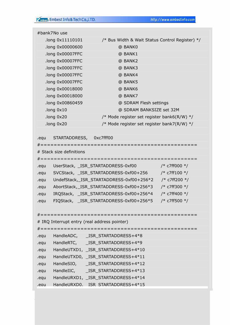
SMRDATA:
#bank0 16bit BOOT ROM
#bank1 NandFlash(8bit)/IDE/USB/rtl8019as/LCD
#bank2 No use
#bank3 Keyboard
#bank4 No use
#bank5 No use
#bank616bit SDRAM
Page 48
Copyright ©2001-2004 Embest Info&Tech Co.,LTD. All rights reserved. Page 48
#bank7 No use
.long 0x11110101 /* Bus Width & Wait Status Control Register) */
.long 0x00000600 @ BANK0
.long 0x00007FFC @ BANK1
.long 0x00007FFC @ BANK2
.long 0x00007FFC @ BANK3
.long 0x00007FFC @ BANK4
.long 0x00007FFC @ BANK5
.long 0x00018000 @ BANK6
.long 0x00018000 @ BANK7
.long 0x00860459 @ SDRAM Flesh settings
.long 0x10 @ SDRAM BANKSIZE set 32M
.long 0x20 /* Mode register set register bank6(R/W) */
.long 0x20 /* Mode register set register bank7(R/W) */
.equ STARTADDRESS, 0xc7fff00
#===============================================
# Stack size definitions
#===============================================
.equ UserStack, _ISR_STARTADDRESS-0xf00 /* c7ff000 */
.equ SVCStack, _ISR_STARTADDRESS-0xf00+256 /* c7ff100 */
.equ UndefStack,_ISR_STARTADDRESS-0xf00+256*2 /* c7ff200 */
.equ AbortStack, _ISR_STARTADDRESS-0xf00+256*3 /* c7ff300 */
.equ IRQStack, _ISR_STARTADDRESS-0xf00+256*4 /* c7ff400 */
.equ FIQStack, _ISR_STARTADDRESS-0xf00+256*5 /* c7ff500 */
#===============================================
# IRQ Interrupt entry (real address pointer)
#===============================================
.equ HandleADC, _ISR_STARTADDRESS+4*8
.equ HandleRTC, _ISR_STARTADDRESS+4*9
.equ HandleUTXD1, _ISR_STARTADDRESS+4*10
.equ HandleUTXD0, _ISR_STARTADDRESS+4*11
.equ HandleSIO, _ISR_STARTADDRESS+4*12
.equ HandleIIC, _ISR_STARTADDRESS+4*13
.equ HandleURXD1, _ISR_STARTADDRESS+4*14
.equ HandleURXD0, ISR STARTADDRESS+4*15
Page 49
.equ HandleTIMER5, _ISR_STARTADDRESS+4*16
.equ HandleTIMER4, _ISR_STARTADDRESS+4*17
.equ HandleTIMER3, _ISR_STARTADDRESS+4*18
.equ HandleTIMER2, _ISR_STARTADDRESS+4*19
.equ HandleTIMER1, _ISR_STARTADDRESS+4*20
.equ HandleTIMER0, _ISR_STARTADDRESS+4*21
.equ HandleUERR01, _ISR_STARTADDRESS+4*22
.equ HandleWDT, _ISR_STARTADDRESS+4*23
.equ HandleBDMA1, _ISR_STARTADDRESS+4*24
.equ HandleBDMA0, _ISR_STARTADDRESS+4*25
.equ HandleZDMA1, _ISR_STARTADDRESS+4*26
.equ HandleZDMA0, _ISR_STARTADDRESS+4*27
.equ HandleTICK, _ISR_STARTADDRESS+4*28
.equ HandleEINT4567,_ISR_STARTADDRESS+4*29
.equ HandleEINT3, _ISR_STARTADDRESS+4*30
.equ HandleEINT2, _ISR_STARTADDRESS+4*31
.equ HandleEINT1, _ISR_STARTADDRESS+4*32
.equ HandleEINT0, _ISR_STARTADDRESS+4*33 /* 0xc7fff84 */
Copyright ©2001-2004 Embest Info&Tech Co.,LTD. All rights reserved. Page 49
Page 50
4.3 µCOS-II
4.3.1 Overview
µCOS-II is the upgraded version of µCOS. Having been widely used at
modern commerce and being verified to have great stability and reliability by
relevant authorities, µCOS-II products have been applied successfully at
famous science research projects such as life science and aerospace project.
Due to the small size of the inner core, it is especially applicable for built-in
system development that has strict requirement on storage space of program
code.
µCOS-I is a real-time operating system with public source codes. It
actually supports synchronic operation of multiple tasks, provides independent
stacks for each task and provides system service and interruption
management function. As a practical and real time operating system, µCOS-II
also has following features:
Portable
ROMable
Scalable
Preemptive
The successfully operated µCOS-II system in teaching system used simple
inner core and user’s program which has been compiled, debugged, and
passed. By using Embest IDE for ARM, you can view all kinds of status of the
inner core, including task, queue, semaphore, mailbox, event, mutex etc. and
at the same time it provides time-related functions, stack and operations of
memory application and release etc.
4.3.2 Debugging and Development Instruction of µCOS-II
Copyright ©2001-2004 Embest Info&Tech Co.,LTD. All rights reserved. Page 50
Page 51
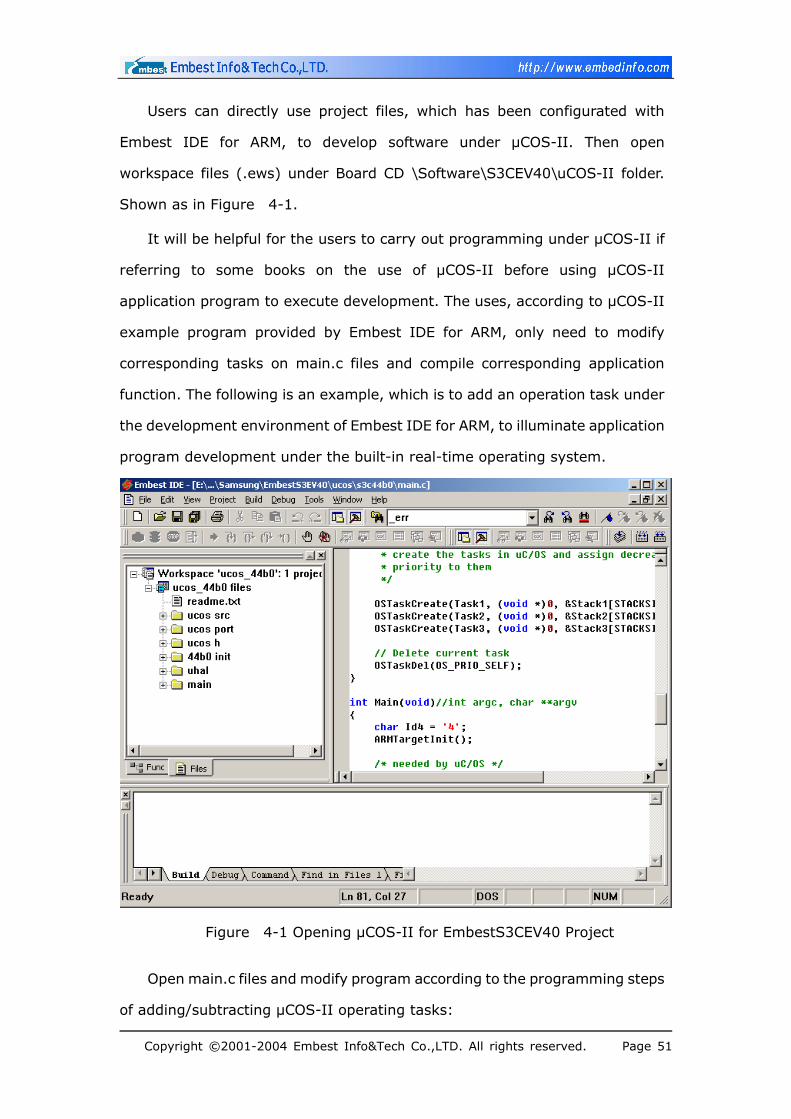
Users can directly use project files, which has been configurated with
Embest IDE for ARM, to develop software under µCOS-II. Then open
workspace files (.ews) under Board CD \Software\S3CEV40\uCOS-II folder.
Shown as in Figure 4-1.
It will be helpful for the users to carry out programming under µCOS-II if
referring to some books on the use of µCOS-II before using µCOS-II
application program to execute development. The uses, according to µCOS-II
example program provided by Embest IDE for ARM, only need to modify
corresponding tasks on main.c files and compile corresponding application
function. The following is an example, which is to add an operation task under
the development environment of Embest IDE for ARM, to illuminate application
program development under the built-in real-time operating system.
Figure 4-1 Opening µCOS-II for EmbestS3CEV40 Project
Open main.c files and modify program according to the programming steps
of adding/subtracting µCOS-II operating tasks:
Copyright ©2001-2004 Embest Info&Tech Co.,LTD. All rights reserved. Page 51
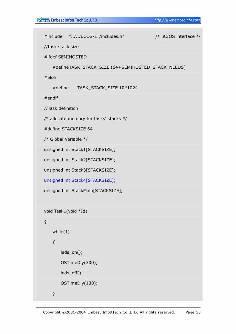
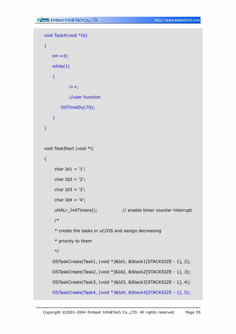
Page 52
Allocate Task Stack(unsigned int Stack4[STACKSIZE];)
To provide variable and stack with storing and accessing space when
operating applications
unsigned int Stack4[STACKSIZE];
Establish Task Functions (void Task4(void *Id))
void Task4(void *Id)
{
initialization and valaribles definition
functions call or instruction set
OSTimeDly(100); //suspended the task
}
Start Task Description ( OSTaskCreate(Task4, (void *)0,
&Stack4[STACKSIZE - 1], 5);)
void TaskStart (void *Id)
{
……
char Id4 = '4';
……
OSTaskCreate(Task4, (void *)0, &Stack4[STACKSIZE - 1], 5);
……
}
Add function module to be initialized into main() function
The following is the content of main.c files after above modifications.
Copyright ©2001-2004 Embest Info&Tech Co.,LTD. All rights reserved. Page 52
Page 53
#include "../../uCOS-II /includes.h" /* uC/OS interface */
//task stack size
#ifdef SEMIHOSTED
#define TASK_STACK_SIZE (64+SEMIHOSTED_STACK_NEEDS)
#else
#define TASK_STACK_SIZE 10*1024
#endif
//Task definition
/* allocate memory for tasks' stacks */
#define STACKSIZE 64
/* Global Variable */
unsigned int Stack1[STACKSIZE];
unsigned int Stack2[STACKSIZE];
unsigned int Stack3[STACKSIZE];
unsigned int Stack4[STACKSIZE];
unsigned int StackMain[STACKSIZE];
void Task1(void *Id)
{
while(1)
{
leds_on();
OSTimeDly(300);
leds_off();
OSTimeDly(130);
}
Copyright ©2001-2004 Embest Info&Tech Co.,LTD. All rights reserved. Page 53
Page 54
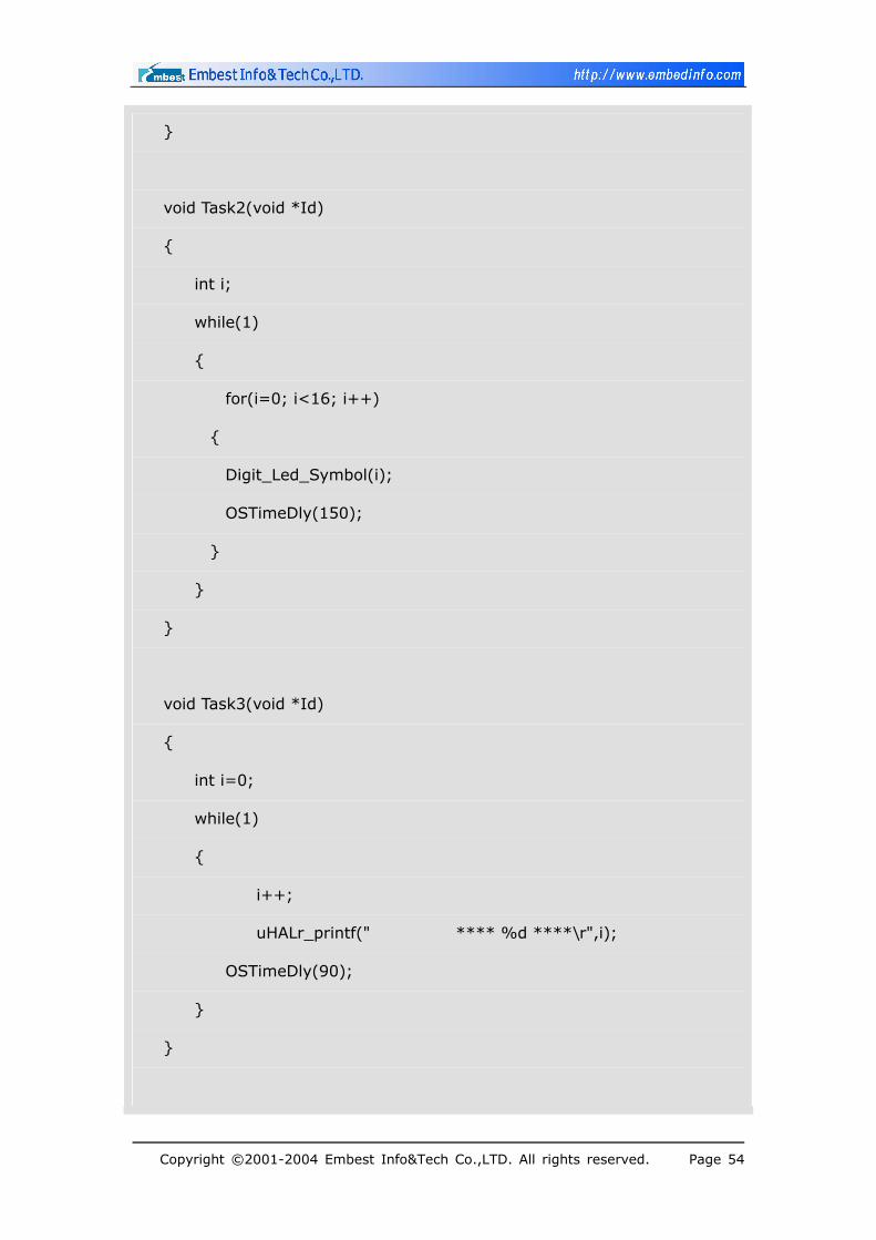
}
void Task2(void *Id)
{
int i;
while(1)
{
for(i=0; i<16; i++)
{
Digit_Led_Symbol(i);
OSTimeDly(150);
}
}
}
void Task3(void *Id)
{
int i=0;
while(1)
{
i++;
uHALr_printf(" **** %d ****\r",i);
OSTimeDly(90);
}
}
Copyright ©2001-2004 Embest Info&Tech Co.,LTD. All rights reserved. Page 54
Page 55
void Task4(void *Id)
{
int i=0;
while(1)
{
i++;
//user function
OSTimeDly(70);
}
}
void TaskStart (void *i)
{
char Id1 = '1';
char Id2 = '2';
char Id3 = '3';
char Id4 = '4';
uHALr_InitTimers(); // enable timer counter interrupt
/*
* create the tasks in uC/OS and assign decreasing
* priority to them
*/
OSTaskCreate(Task1, (void *)&Id1, &Stack1[STACKSIZE - 1], 2);
OSTaskCreate(Task2, (void *)&Id2, &Stack2[STACKSIZE - 1], 3);
OSTaskCreate(Task3, (void *)&Id3, &Stack3[STACKSIZE - 1], 4);
OSTaskCreate(Task4, (void *)&Id4, &Stack4[STACKSIZE - 1], 5);
Copyright ©2001-2004 Embest Info&Tech Co.,LTD. All rights reserved. Page 55
Page 56
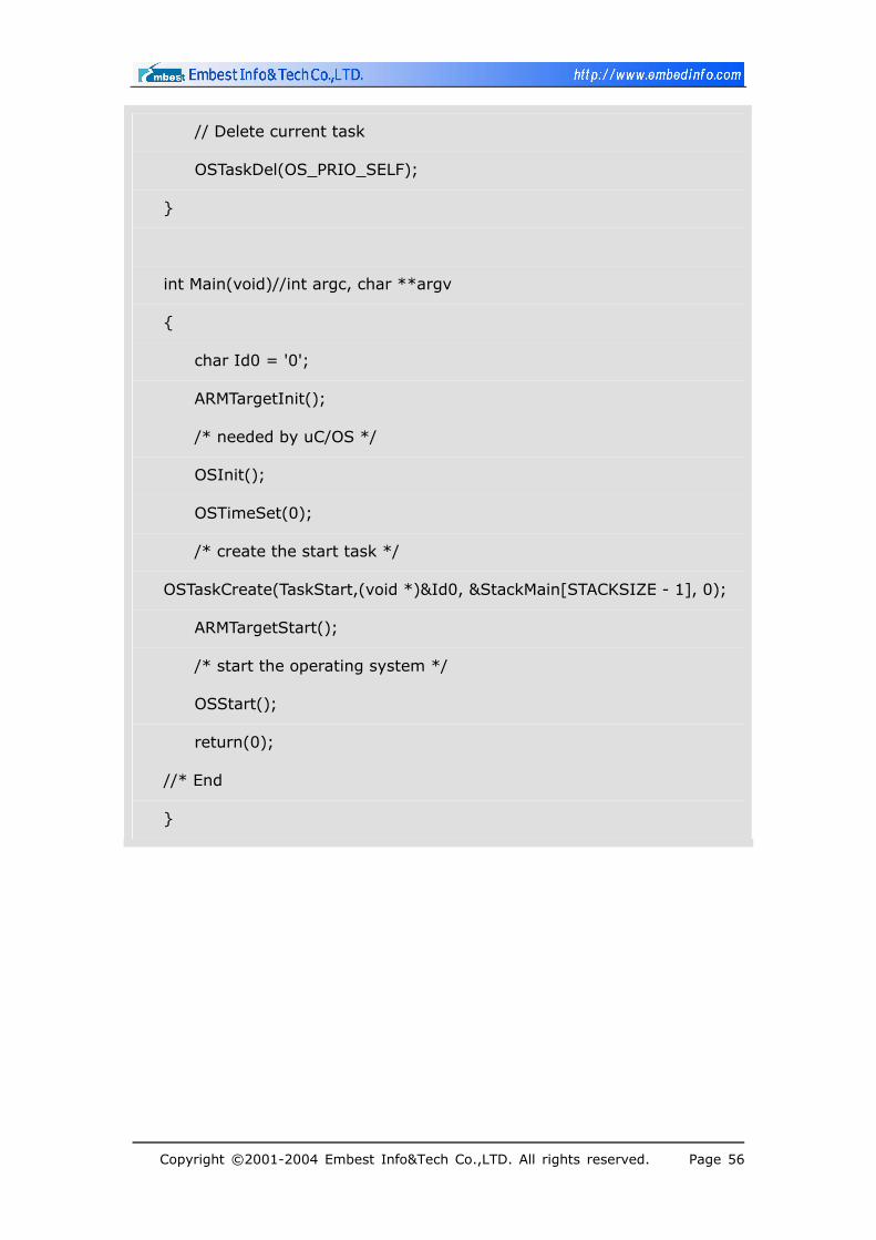
// Delete current task
OSTaskDel(OS_PRIO_SELF);
}
int Main(void)//int argc, char **argv
{
char Id0 = '0';
ARMTargetInit();
/* needed by uC/OS */
OSInit();
OSTimeSet(0);
/* create the start task */
OSTaskCreate(TaskStart,(void *)&Id0, &StackMain[STACKSIZE - 1], 0);
ARMTargetStart();
/* start the operating system */
OSStart();
return(0);
//* End
}
Copyright ©2001-2004 Embest Info&Tech Co.,LTD. All rights reserved. Page 56
Page 57
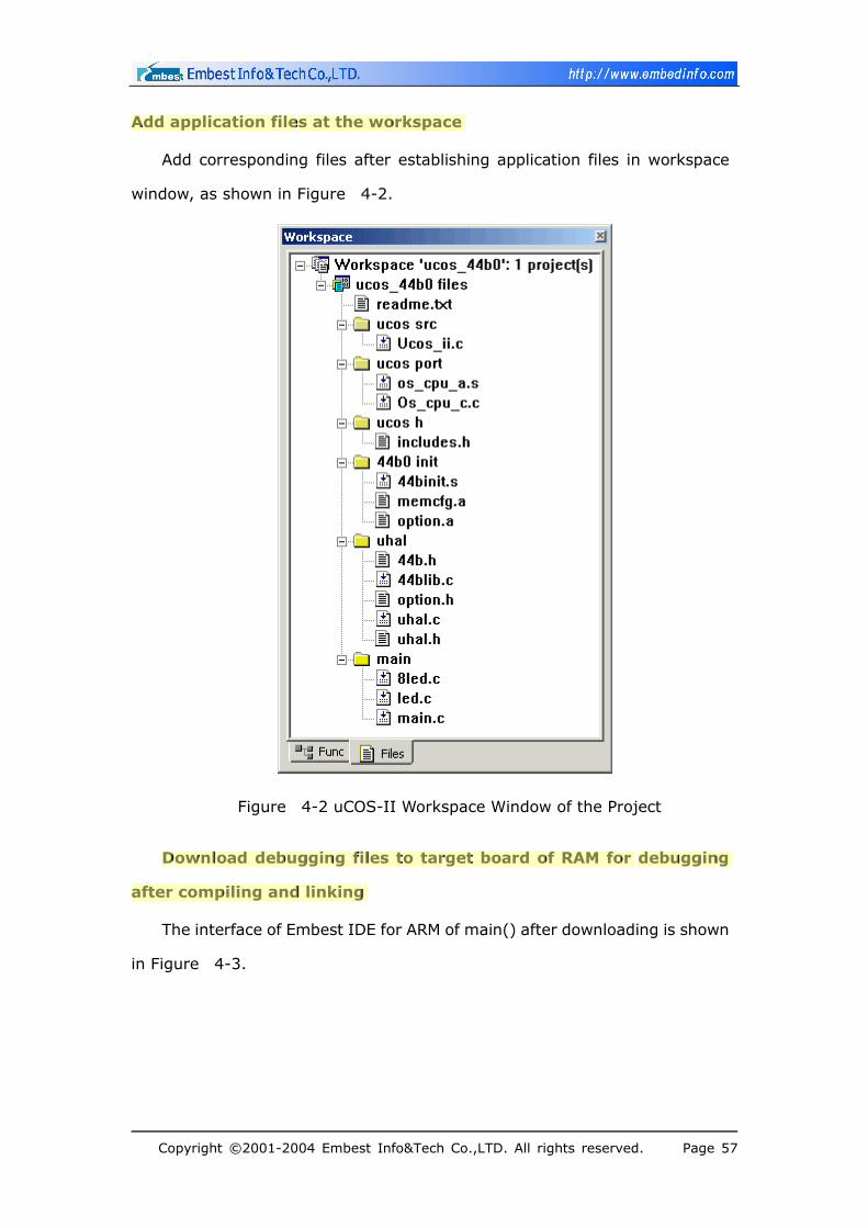
Add application files at the workspace
Add corresponding files after establishing application files in workspace
window, as shown in Figure 4-2.
Figure 4-2 uCOS-II Workspace Window of the Project
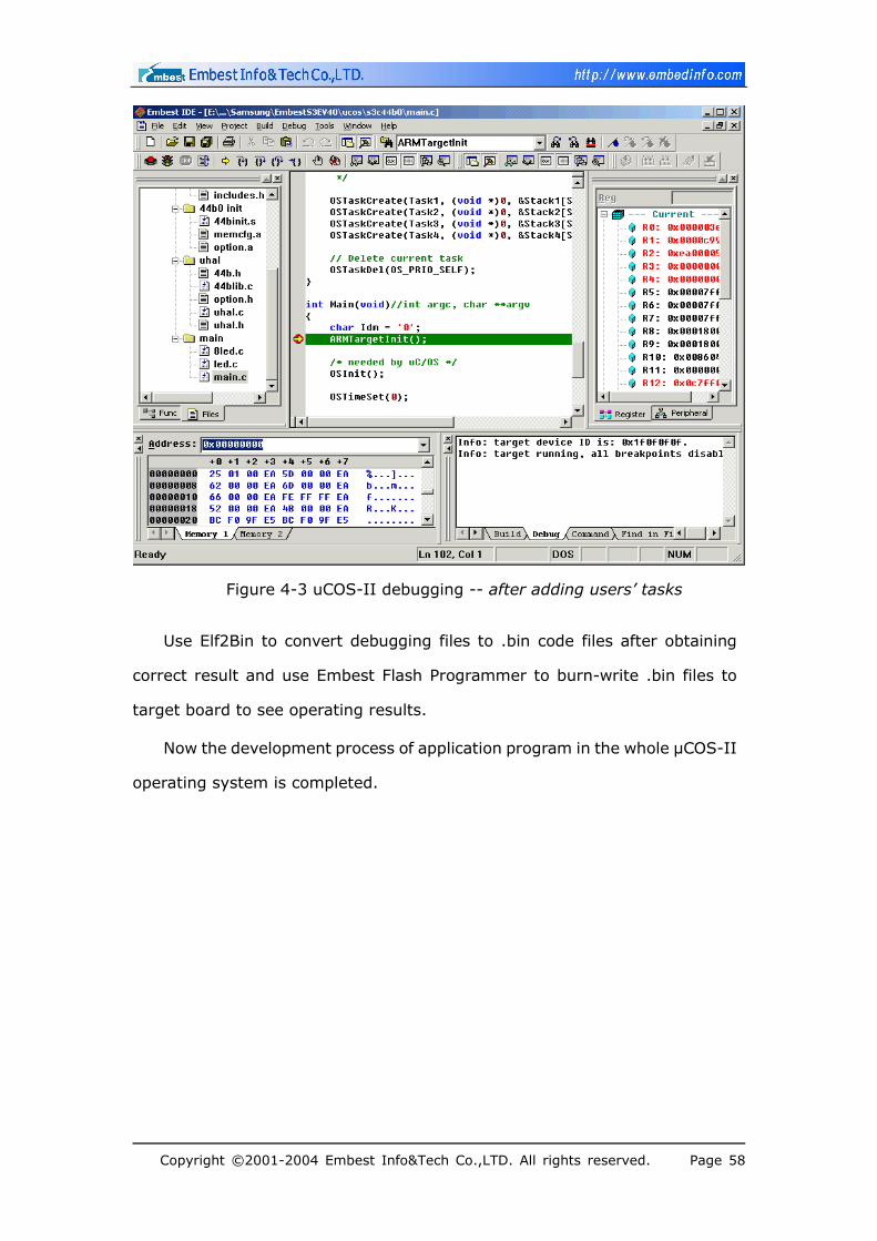
Download debugging files to target board of RAM for debugging
after compiling and linking
The interface of Embest IDE for ARM of main() after downloading is shown
in Figure 4-3.
Copyright ©2001-2004 Embest Info&Tech Co.,LTD. All rights reserved. Page 57
Page 58
Figure 4-3 uCOS-II debugging -- after adding users’ tasks
Use Elf2Bin to convert debugging files to .bin code files after obtaining
correct result and use Embest Flash Programmer to burn-write .bin files to
target board to see operating results.
Now the development process of application program in the whole µCOS-II
operating system is completed.
Copyright ©2001-2004 Embest Info&Tech Co.,LTD. All rights reserved. Page 58
Page 59
4.4 Example Codes
Example 1: the usage of timer
Workspace file location: Board CD \Software\S3CEV40\timer_test
Function: To make users be aware of the working mode of the timer and
the usage of the register.
Example 2: the usage of I/O port
Workspace file location: Board CD \Software\S3CEV40\led_test
Function: To master I/O programming skills by configuring and using I/O
port of the processor.
Example 3: transceiving of RS232 serial ports
Workspace file location: Board CD \Software\S3CEV40\ UART_test
Function: To control the communication between processor and PC
through interactive input; to master controlling method of serial ports
programming
Example 4: the usage of 7-digit LED
Workspace file location: Board CD \Software\S3CEV40\ 8Led_test
Function: To master the definition and usage of address wire and data wire
of the processor
Example 5: the usage of 4 x 4 keyboard
Workspace file location: Board CD \Software\S3CEV40\ keyboard_test
Function: To master the definition and usage of address wire and data wire
of the processor
Example 6: reading and writing in E2PROM of IIC port
Workspace file location: Board CD \Software\S3CEV40\ iic_test
Function: to read and write serial signals in E2PROM devices; to provide
methods of programming reading and writing control.
Example 7: voice control of IIS port
Copyright ©2001-2004 Embest Info&Tech Co.,LTD. All rights reserved. Page 59
Page 60
Workspace file location: Board CD \Software\S3CEV40\iis_test
Function: To realize signal programming and outputting of audio port and
master programming methods for IIS port of the built-in processor
Example 8: controlling LCD display
Workspace file location: Board CD \Software\S3CEV40\lcd_test
Or Board CD \Software\S3CEV40\Bmp_Display
Function: To master the usage of LCD drive of S3C44b0 processor and
provide abundant program controlling codes including pixel control, color
control, letter database and drawing dots and drawing lines etc.
Example 9: controlling touch screen
Workspace file location: Board CD \Software\S3CEV40\ TouchScreen_Test
Function: Advanced program application of the processor: to master
operating principles and programming methods of man machine interface.
Example 10: realizing TFTP control protocol
Workspace file location: Board CD \Software\S3CEV40\tftp_test
Function: To realize files transport of Ethernet interface and save the data
files on the Flash chip through controlling and programming of the net card
chip.
Example 11: realizing DHCP control protocol
Workspace file location: Board CD \Software\S3CEV40\dhcp_test
Function: To conFigure dynamic IP and UDP transport protocol through
controlling and programming of the net card chip.
Example 12: the usage of µCOS-II operating system
Workspace file location: Board CD \Software\S3CEV40\uCOS-II
Function: To provide programming methods of real-time operating system
and the application under real-time operating system.
More test program, please read the \Software\S3CEV40\Readme.txt
Copyright ©2001-2004 Embest Info&Tech Co.,LTD. All rights reserved. Page 60
Page 61
Chapter V Customer Service
Get support on demand. Connect Customer Service for more information
on how to use the Embest’s products.
Web Site Get the latest information and docs about Embest’s products from the web
site: http://www.embedinfo.com
You may have noticed some trouble issues at the support forums. In the
meantime, you can get help by subscribing to the following forum:
http://www.embedinfo.com/cforum/arm_forum_login.asp
E-Mail If you have any question, comments, feedback or suggestions as to how
our products could be improved, let us know at [email protected]
Telephone Number
You can also call 86-755-25635626 with the extension to the Customer Service Center.
Fax Number
Our fax number is 86-755-25616057.
Warning:
Pay attention to anti-static protection. Exceeding any Maximum value, the
static can harm the products permanently. Critical State is not recommended
when using this product.
Copyright ©2001-2004 Embest Info&Tech Co.,LTD. All rights reserved. Page 61
Page 62
Appendix A Jumper and Switch Set
Figure A-1 SW1 and SW2 Set
SW1、SW2(Jumper) Function
All Connection Serial Port UART1 can be used normally
Disconnection Reserve I/O port of UART1 for customers’ use
Figure A-2 SW3 Set
SW3(Jumper) Function
Connection
Disconnection
This Jumper is reserved and not used
temporarily
Figure A-3 SW4 Set
SW4(Jumper) Function
Connection
Disconnection
This Jumper is reserved and not used
temporarily
Figure A-4 SW5 Set
SW5(Jumper) Function
Connection Select Little endian Mode
Disconnection Select Big endian Mode
Figure A-5 SW6 Set
SW6(Switch) Function
USBPOWER Development Board is powered through USB
EXTPOWER Development Board is powered by external 5V DC
regulated power supply
Copyright ©2001-2004 Embest Info&Tech Co.,LTD. All rights reserved. Page 62