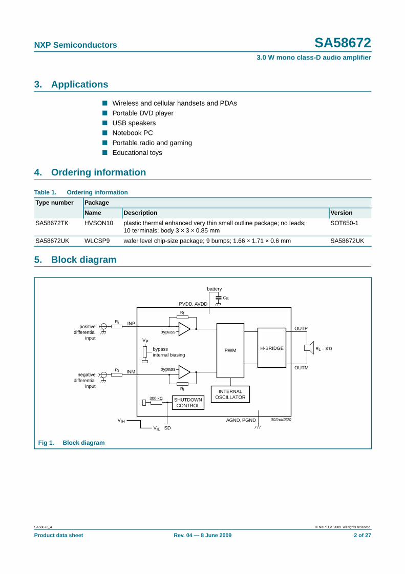
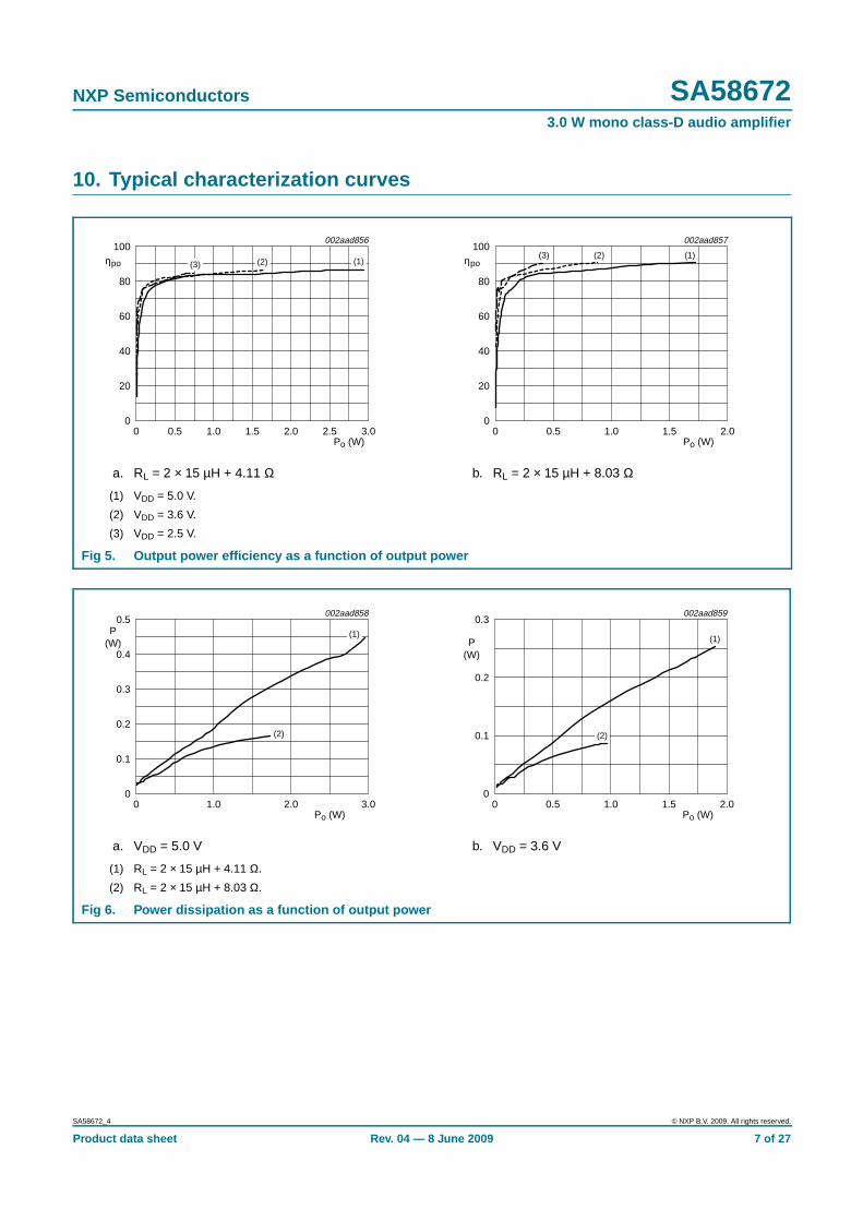
1. General description The SA58672 is a mono, filter-free class-D audio amplifier which is available in a 9 bump WLCSP (Wafer Level Chip-Size Package) and 10-terminal HVSON packages. The SA58672 features shutdown control. Improved immunity to noise and RF rectification is increased by high PSRR and differential circuit topology. Fast start-up time and very small WLCSP package makes it an ideal choice for both cellular handsets and PDAs. The SA58672 delivers 1.7 W at 5 V and 800 mW at 3.6 V into 8 Ω. It delivers 3.0 W at 5 V and 1.6 W at 3.6 V into 4 Ω. The maximum power efficiency is excellent at 90 % into 8 Ω and 84 % to 88 % into 4 Ω. The SA58672 provides thermal and short-circuit shutdown protection. 2. Features ■ Output power ◆ 3.0 W into 4 Ω at 5 V ◆ 1.6 W into 4 Ω at 3.6 V ◆ 1.7 W into 8 Ω at 5 V ◆ 800 mW into 8 Ω at 3.6 V ■ Power supply range: 2.0 V to 5.5 V ■ Shutdown control ■ High SVRR: -77 dB at 217 Hz ■ Fast start-up time: 7.0 ms ■ Low supply current ■ Low shutdown current ■ Short-circuit and thermal protection ■ Space savings with 1.66 mm × 1.71 mm × 0.6 mm 9 bump WLCSP package ■ Low junction to ambient thermal resistance of 100 K/W with adequate heat sinking of WLCSP ■ Enhanced power dissipation with 3.0 mm × 3.0 mm × 0.85 mm HVSON10 package SA58672 3.0 W mono class-D audio amplifier Rev. 04 — 8 June 2009 Product data sheet
Transcript
1. General description
The SA58672 is a mono, filter-free class-D audio amplifier which is available in a 9 bumpWLCSP (Wafer Level Chip-Size Package) and 10-terminal HVSON packages.
The SA58672 features shutdown control. Improved immunity to noise and RF rectificationis increased by high PSRR and differential circuit topology. Fast start-up time and verysmall WLCSP package makes it an ideal choice for both cellular handsets and PDAs.
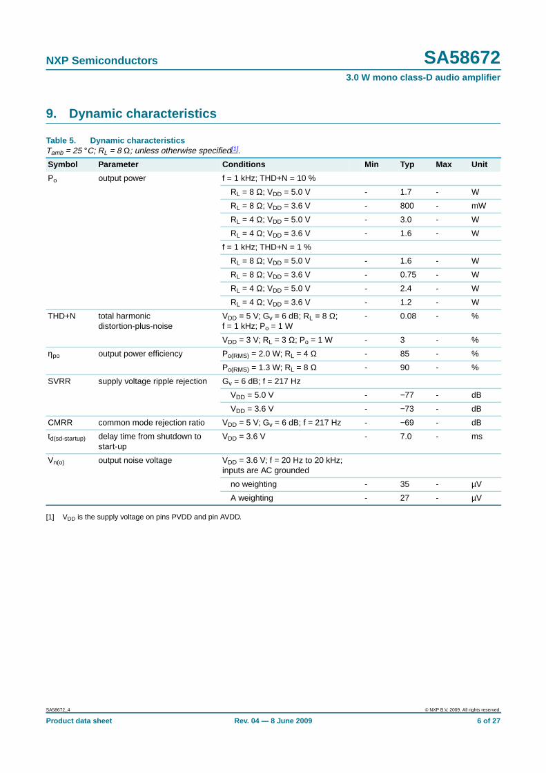
The SA58672 delivers 1.7 W at 5 V and 800 mW at 3.6 V into 8 Ω. It delivers 3.0 W at 5 Vand 1.6 W at 3.6 V into 4 Ω. The maximum power efficiency is excellent at 90 % into 8 Ωand 84 % to 88 % into 4 Ω. The SA58672 provides thermal and short-circuit shutdownprotection.
2. Features
n Output power
u 3.0 W into 4 Ω at 5 V
u 1.6 W into 4 Ω at 3.6 V
u 1.7 W into 8 Ω at 5 V
u 800 mW into 8 Ω at 3.6 V
n Power supply range: 2.0 V to 5.5 V
n Shutdown control
n High SVRR: −77 dB at 217 Hz
n Fast start-up time: 7.0 ms
n Low supply current
n Low shutdown current
n Short-circuit and thermal protection
n Space savings with 1.66 mm × 1.71 mm × 0.6 mm 9 bump WLCSP package
n Low junction to ambient thermal resistance of 100 K/W with adequate heat sinking ofWLCSP
n Enhanced power dissipation with 3.0 mm × 3.0 mm × 0.85 mm HVSON10 package
SA586723.0 W mono class-D audio amplifierRev. 04 — 8 June 2009 Product data sheet
NXP Semiconductors SA586723.0 W mono class-D audio amplifier
3. Applications
n Wireless and cellular handsets and PDAs
n Portable DVD player
n USB speakers
n Notebook PC
n Portable radio and gaming
n Educational toys
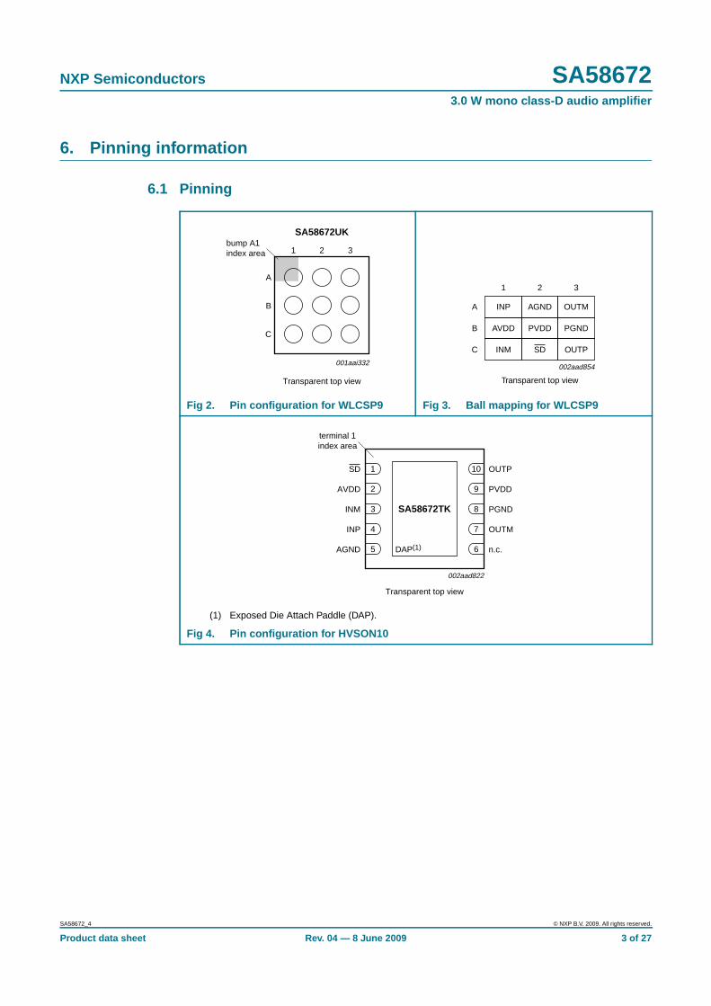
4. Ordering information
5. Block diagram
Table 1. Ordering information
Type number Package
Name Description Version
SA58672TK HVSON10 plastic thermal enhanced very thin small outline package; no leads;10 terminals; body 3 × 3 × 0.85 mm
NXP Semiconductors SA586723.0 W mono class-D audio amplifier
11. Application information
11.1 Power supply decoupling considerationsThe SA58672 is a mono class-D audio amplifier that requires proper power supplydecoupling to ensure the rated performance for THD+N and power efficiency. To decouplehigh frequency transients, power supply spikes and digital noise on the power bus line, alow Equivalent Series Resistance (ESR) capacitor, of typically 1 µF is placed as close aspossible to the PVDD terminals of the device. It is important to place the decouplingcapacitor at the power pins of the device because any resistance or inductance in thePCB trace between the device and the capacitor can cause a loss in efficiency. Additionaldecoupling using a larger capacitor, 4.7 µF or greater may be done on the power supplyconnection on the PCB to filter low frequency signals. Usually this is not required due tohigh PSRR of the device.
11.2 Voltage gainThe SA58672 is comprised of an analog amplifier stage and a comparator stage. Theoutput of the analog amplifier stage is compared with the periodic ramp signal from thesawtooth ramp generator. The resulting output of the comparator is a Pulse WidthModulated (PWM) signal. The final stage is a power NMOS and PMOS H-bridge thatconverts the PWM into a high power output signal capable of driving low-impedanceloads.
The input resistor, Ri sets the gain of the amplifier according to Equation 1:
(1)
11.3 Input capacitor selectionThe SA58672 does not require input coupling capacitors when used with a differentialaudio source that is biased from 0.5 V to VDD − 0.8 V. In other words, the input signal mustbe biased within the common-mode input voltage range. If high-pass filtering is requiredor if it is driven using a single-ended source, input coupling capacitors are required.
The 3 dB cut-off frequency created by the input coupling capacitor and the input resistorsis calculated by Equation 2:
(2)
Using an input resistor of 150 kΩ, the gain is set to 2 V/V. At this gain setting, for inputcapacitor values from 220 nF to 2.2 µF, the 3 dB cut-off frequency may be set between22 Hz and 220 Hz. Since the values of the input coupling capacitor and the input resistoraffects the low frequency performance of the audio amplifier, it is important to consider inthe system design. Small speakers in wireless and cellular phones usually do not respondwell to low frequency signals. Their low frequency response may be only 600 Hz; typically1 kHz. Thus, the 3 dB cut-off frequency should be increased to block the low frequencysignals to the speakers.
NXP Semiconductors SA586723.0 W mono class-D audio amplifier
For a required 3 dB cut-off frequency, Equation 3 is used to determine Ci:
(3)
The input signal may be DC-coupled, but not using input coupling capacitors mayincrease the output offset voltage.
11.4 PCB layout considerationsThe component location is very important for performance of the SA58672. Place allexternal components very close to the device. Placing decoupling capacitors directly atthe power supply pins increases efficiency because the resistance and inductance in thetrace between the device power supply pins and the decoupling capacitor causes a loss inpower efficiency.
The trace width and routing are also very important for power output and noiseconsiderations.
For high current terminals (PVDD, PGND and audio output), the trace widths should bemaximized to ensure proper performance and output power. Use at least 500 µm widetraces.
For the input pins (INP, INM), the traces must be symmetrical and run side-by-side tomaximize common-mode cancellation.
11.5 Evaluation demo boardThe SA58672 evaluation demo board schematic is shown in Figure 14. An evaluationdemo board is available and it may be used for either differential or single-ended (SE)input configuration. A component position on the PCB is provided to AC ground one of theinputs using a 0 Ω chip resistor. When driving SE, the undriven input must be at the sameDC level as driven input. If the input is driven from an iPOD or MP3 player, the undriveninput is AC grounded; however, if driven from a CODEC, the undriven input is ACdecoupled to the same level as the CODEC output. Usually, a Vref is provided on theCODEC.
Ci1
2π Ri× f 3dB–×--------------------------------------=
NXP Semiconductors SA586723.0 W mono class-D audio amplifier
11.6 Filter-free operation and ferrite bead filtersA ferrite bead low-pass filter can be used to reduce radio frequency emissions inapplications that have circuits sensitive to greater than 1 MHz. A ferrite bead low-passfilter functions well for amplifiers that must pass FCC unintentional radiation requirementsat greater than 30 MHz. Choose a bead with high-impedance at high frequencies and verylow-impedance at low frequencies. In order to prevent distortion of the output signal,select a ferrite bead with adequate current rating.
Ferrite bead sources are:
• TDK MPZ1608S221A: 220 Ω at 100 MHz; 3 A peak max current;0.04 Ω DC resistance.
• KOA CZP2AFTTD221P: 220 Ω at 100 MHz; 2 A peak max current;0.05 Ω DC resistance.
• Murata BLM21PG221SN1: 220 Ω at 100 MHz; 2 A peak max current;0.05 Ω DC resistance.
The DC resistance should be as low as possible and the maximum current must exceed atleast 1 A. Impedance of 220 Ω at 100 MHz is common spec, but 600 Ω and 1 kΩ ferritebeads may be used. Generally, the current rating decreases with increasing impedance at100 MHz. However, larger impedance at 100 MHz allows for a smaller, shunt capacitorthat will reduce the quiescent load current; this is important for battery operatedapplications.
R3 and R4 are not populated for differential input drive. For single-ended input drive, either R3 or R4 are shorted to groundusing a 0 Ω resistor (i.e., one input is AC grounded and the other is driven with the input signal).
NXP Semiconductors SA586723.0 W mono class-D audio amplifier
For applications in which there are circuits that are EMI sensitive to low frequency(< 1 MHz) and there are long leads from amplifier to speaker, it may be necessary to usean LC output filter.
11.7 Efficiency and thermal considerationsThe maximum ambient operating temperature depends on the heat transferring ability ofthe heat spreader on the PCB layout. In Table 3 “Limiting values”, power dissipation, thepower derating factor is given as 10 mW/K. The device thermal resistance, Rth(j-a) is thereciprocal of the power derating factor. Convert the power derating factor to Rth(j-a) byEquation 4:
(4)
For a maximum allowable junction temperature, Tj = 150 °C and Rth(j-a) = 100 K/W and amaximum device dissipation of 0.84 W (420 mW per channel) and for 1.7 W per channeloutput power, 4 Ω load, 5 V supply, the maximum ambient temperature is calculated usingEquation 5:
(5)
The maximum ambient temperature is 66 °C at maximum power dissipation for 5 V supplyand 4 Ω load. If the junction temperature of the SA58672 rises above 150 °C, the thermalprotection circuitry turns the device off; this prevents damage to the IC. Using speakersgreater than 4 Ω further enhances thermal performance and battery lifetime by reducingthe output load current and increasing amplifier efficiency.
11.8 Additional thermal informationThe SA58672 9 bump WLCSP package ground bumps are soldered directly to the PCBheat spreader. By the use of thermal vias, the bumps may be soldered directly to a groundplane or special heat sinking layer designed into the PCB. The thickness and area of theheat spreader may be maximized to optimize heat transfer and achieve lower packagethermal resistance.
The SA58672 HVSON10 package has an exposed Die Attach Paddle (DAP), which issoldered directly to the PCB heat spreader to provide enhanced heat transfer and achievelowest package thermal resistance.
NXP Semiconductors SA586723.0 W mono class-D audio amplifier
12. Test information
12.1 Test setup for typical characterization curvesThe SA58672 demo board shown in Figure 14 and the APA (Audio Precision Analyzer)are used to provide the characterization curves. The test setup diagram in Figure 15shows the setup details. The output load configuration is comprised of 2 × 15 µH powerinductors and precision power load resistor. This passive load emulates a small, lowpower speaker; it facilitates efficiency measurements. A speaker may be substituted forthe passive load to yield similar results.
NXP Semiconductors SA586723.0 W mono class-D audio amplifier
14. Soldering of SMD packages
This text provides a very brief insight into a complex technology. A more in-depth accountof soldering ICs can be found in Application Note AN10365 “Surface mount reflowsoldering description”.
14.1 Introduction to solderingSoldering is one of the most common methods through which packages are attached toPrinted Circuit Boards (PCBs), to form electrical circuits. The soldered joint provides boththe mechanical and the electrical connection. There is no single soldering method that isideal for all IC packages. Wave soldering is often preferred when through-hole andSurface Mount Devices (SMDs) are mixed on one printed wiring board; however, it is notsuitable for fine pitch SMDs. Reflow soldering is ideal for the small pitches and highdensities that come with increased miniaturization.
14.2 Wave and reflow solderingWave soldering is a joining technology in which the joints are made by solder coming froma standing wave of liquid solder. The wave soldering process is suitable for the following:
• Through-hole components
• Leaded or leadless SMDs, which are glued to the surface of the printed circuit board
Not all SMDs can be wave soldered. Packages with solder balls, and some leadlesspackages which have solder lands underneath the body, cannot be wave soldered. Also,leaded SMDs with leads having a pitch smaller than ~0.6 mm cannot be wave soldered,due to an increased probability of bridging.
The reflow soldering process involves applying solder paste to a board, followed bycomponent placement and exposure to a temperature profile. Leaded packages,packages with solder balls, and leadless packages are all reflow solderable.
Key characteristics in both wave and reflow soldering are:
• Board specifications, including the board finish, solder masks and vias
• Package footprints, including solder thieves and orientation
• The moisture sensitivity level of the packages
• Package placement
• Inspection and repair
• Lead-free soldering versus SnPb soldering
14.3 Wave solderingKey characteristics in wave soldering are:
• Process issues, such as application of adhesive and flux, clinching of leads, boardtransport, the solder wave parameters, and the time during which components areexposed to the wave
• Solder bath specifications, including temperature and impurities
NXP Semiconductors SA586723.0 W mono class-D audio amplifier
14.4 Reflow solderingKey characteristics in reflow soldering are:
• Lead-free versus SnPb soldering; note that a lead-free reflow process usually leads tohigher minimum peak temperatures (see Figure 18) than a SnPb process, thusreducing the process window
• Solder paste printing issues including smearing, release, and adjusting the processwindow for a mix of large and small components on one board
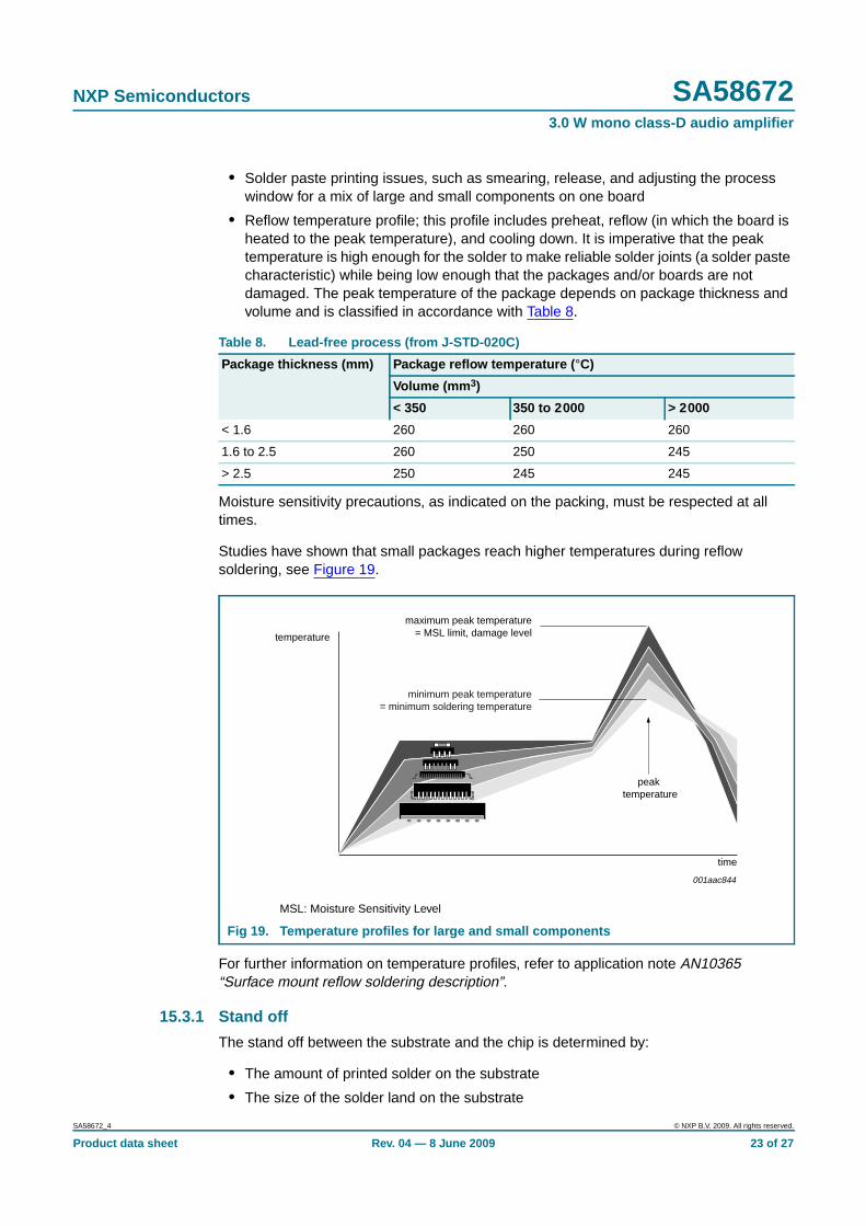
• Reflow temperature profile; this profile includes preheat, reflow (in which the board isheated to the peak temperature) and cooling down. It is imperative that the peaktemperature is high enough for the solder to make reliable solder joints (a solder pastecharacteristic). In addition, the peak temperature must be low enough that thepackages and/or boards are not damaged. The peak temperature of the packagedepends on package thickness and volume and is classified in accordance withTable 6 and 7
Moisture sensitivity precautions, as indicated on the packing, must be respected at alltimes.
Studies have shown that small packages reach higher temperatures during reflowsoldering, see Figure 18.
Table 6. SnPb eutectic process (from J-STD-020C)
Package thickness (mm) Package reflow temperature ( °C)
Volume (mm 3)
< 350 ≥ 350
< 2.5 235 220
≥ 2.5 220 220
Table 7. Lead-free process (from J-STD-020C)
Package thickness (mm) Package reflow temperature ( °C)
NXP Semiconductors SA586723.0 W mono class-D audio amplifier
For further information on temperature profiles, refer to Application Note AN10365“Surface mount reflow soldering description”.
15. Soldering of WLCSP packages
15.1 Introduction to soldering WLCSP packagesThis text provides a very brief insight into a complex technology. A more in-depth accountof soldering WLCSP (Wafer Level Chip-Size Packages) can be found in application noteAN10439 “Wafer Level Chip Scale Package” and in application note AN10365 “Surfacemount reflow soldering description”.
Wave soldering is not suitable for this package.
All NXP WLCSP packages are lead-free.
15.2 Board mountingBoard mounting of a WLCSP requires several steps:
1. Solder paste printing on the PCB
2. Component placement with a pick and place machine
3. The reflow soldering itself
15.3 Reflow solderingKey characteristics in reflow soldering are:
• Lead-free versus SnPb soldering; note that a lead-free reflow process usually leads tohigher minimum peak temperatures (see Figure 19) than a PbSn process, thusreducing the process window
MSL: Moisture Sensitivity Level
Fig 18. Temperature profiles for large and small components
001aac844
temperature
time
minimum peak temperature= minimum soldering temperature
NXP Semiconductors SA586723.0 W mono class-D audio amplifier
• Solder paste printing issues, such as smearing, release, and adjusting the processwindow for a mix of large and small components on one board
• Reflow temperature profile; this profile includes preheat, reflow (in which the board isheated to the peak temperature), and cooling down. It is imperative that the peaktemperature is high enough for the solder to make reliable solder joints (a solder pastecharacteristic) while being low enough that the packages and/or boards are notdamaged. The peak temperature of the package depends on package thickness andvolume and is classified in accordance with Table 8.
Moisture sensitivity precautions, as indicated on the packing, must be respected at alltimes.
Studies have shown that small packages reach higher temperatures during reflowsoldering, see Figure 19.
For further information on temperature profiles, refer to application note AN10365“Surface mount reflow soldering description”.
15.3.1 Stand off
The stand off between the substrate and the chip is determined by:
• The amount of printed solder on the substrate
• The size of the solder land on the substrate
Table 8. Lead-free process (from J-STD-020C)
Package thickness (mm) Package reflow temperature ( °C)
Volume (mm 3)
< 350 350 to 2000 > 2000
< 1.6 260 260 260
1.6 to 2.5 260 250 245
> 2.5 250 245 245
MSL: Moisture Sensitivity Level
Fig 19. Temperature profiles for large and small components
001aac844
temperature
time
minimum peak temperature= minimum soldering temperature
NXP Semiconductors SA586723.0 W mono class-D audio amplifier
• The bump height on the chip
The higher the stand off, the better the stresses are released due to TEC (ThermalExpansion Coefficient) differences between substrate and chip.
15.3.2 Quality of solder joint
A flip-chip joint is considered to be a good joint when the entire solder land has beenwetted by the solder from the bump. The surface of the joint should be smooth and theshape symmetrical. The soldered joints on a chip should be uniform. Voids in the bumpsafter reflow can occur during the reflow process in bumps with high ratio of bump diameterto bump height, i.e. low bumps with large diameter. No failures have been found to berelated to these voids. Solder joint inspection after reflow can be done with X-ray tomonitor defects such as bridging, open circuits and voids.
15.3.3 Rework
In general, rework is not recommended. By rework we mean the process of removing thechip from the substrate and replacing it with a new chip. If a chip is removed from thesubstrate, most solder balls of the chip will be damaged. In that case it is recommendednot to re-use the chip again.
Device removal can be done when the substrate is heated until it is certain that all solderjoints are molten. The chip can then be carefully removed from the substrate withoutdamaging the tracks and solder lands on the substrate. Removing the device must bedone using plastic tweezers, because metal tweezers can damage the silicon. Thesurface of the substrate should be carefully cleaned and all solder and flux residuesand/or underfill removed. When a new chip is placed on the substrate, use the fluxprocess instead of solder on the solder lands. Apply flux on the bumps at the chip side aswell as on the solder pads on the substrate. Place and align the new chip while viewingwith a microscope. To reflow the solder, use the solder profile shown in application noteAN10365 “Surface mount reflow soldering description”.
NXP Semiconductors SA586723.0 W mono class-D audio amplifier
18. Legal information
18.1 Data sheet status
[1] Please consult the most recently issued document before initiating or completing a design.
[2] The term ‘short data sheet’ is explained in section “Definitions”.
[3] The product status of device(s) described in this document may have changed since this document was published and may differ in case of multiple devices. The latest product statusinformation is available on the Internet at URL http://www.nxp.com.
18.2 Definitions
Draft — The document is a draft version only. The content is still underinternal review and subject to formal approval, which may result inmodifications or additions. NXP Semiconductors does not give anyrepresentations or warranties as to the accuracy or completeness ofinformation included herein and shall have no liability for the consequences ofuse of such information.
Short data sheet — A short data sheet is an extract from a full data sheetwith the same product type number(s) and title. A short data sheet is intendedfor quick reference only and should not be relied upon to contain detailed andfull information. For detailed and full information see the relevant full datasheet, which is available on request via the local NXP Semiconductors salesoffice. In case of any inconsistency or conflict with the short data sheet, thefull data sheet shall prevail.
18.3 Disclaimers
General — Information in this document is believed to be accurate andreliable. However, NXP Semiconductors does not give any representations orwarranties, expressed or implied, as to the accuracy or completeness of suchinformation and shall have no liability for the consequences of use of suchinformation.
Right to make changes — NXP Semiconductors reserves the right to makechanges to information published in this document, including withoutlimitation specifications and product descriptions, at any time and withoutnotice. This document supersedes and replaces all information supplied priorto the publication hereof.
Suitability for use — NXP Semiconductors products are not designed,authorized or warranted to be suitable for use in medical, military, aircraft,space or life support equipment, nor in applications where failure ormalfunction of an NXP Semiconductors product can reasonably be expectedto result in personal injury, death or severe property or environmental
damage. NXP Semiconductors accepts no liability for inclusion and/or use ofNXP Semiconductors products in such equipment or applications andtherefore such inclusion and/or use is at the customer’s own risk.
Applications — Applications that are described herein for any of theseproducts are for illustrative purposes only. NXP Semiconductors makes norepresentation or warranty that such applications will be suitable for thespecified use without further testing or modification.
Limiting values — Stress above one or more limiting values (as defined inthe Absolute Maximum Ratings System of IEC 60134) may cause permanentdamage to the device. Limiting values are stress ratings only and operation ofthe device at these or any other conditions above those given in theCharacteristics sections of this document is not implied. Exposure to limitingvalues for extended periods may affect device reliability.
Terms and conditions of sale — NXP Semiconductors products are soldsubject to the general terms and conditions of commercial sale, as publishedat http://www.nxp.com/profile/terms, including those pertaining to warranty,intellectual property rights infringement and limitation of liability, unlessexplicitly otherwise agreed to in writing by NXP Semiconductors. In case ofany inconsistency or conflict between information in this document and suchterms and conditions, the latter will prevail.
No offer to sell or license — Nothing in this document may be interpretedor construed as an offer to sell products that is open for acceptance or thegrant, conveyance or implication of any license under any copyrights, patentsor other industrial or intellectual property rights.
Export control — This document as well as the item(s) described hereinmay be subject to export control regulations. Export might require a priorauthorization from national authorities.
18.4 TrademarksNotice: All referenced brands, product names, service names and trademarksare the property of their respective owners.
19. Contact information
For more information, please visit: http://www .nxp.com
For sales office addresses, please send an email to: salesad [email protected]
Document status [1] [2] Product status [3] Definition
Objective [short] data sheet Development This document contains data from the objective specification for product development.
Preliminary [short] data sheet Qualification This document contains data from the preliminary specification.
Product [short] data sheet Production This document contains the product specification.