Page 1
SAM D20 QTouch Robustness Evaluation Kit
Part Number: ATSAMD20-QTRDEMO
The SAM D20 QTouch Robustness Evaluation kit demonstrates the high capacitive touch performance of the Peripheral Touch Controller (PTC) while achieving best-in-class conducted immunity and moisture tolerance required in home appliance and industrial applications.
The demo is part of the QTouch Safety Platform, key features of the QTouch Safety Platform are:
IEC 61000-4-6 10V Conducted Immunity tolerant QTouch Safety Library
Ships with IEC/UL 60730 Class B certified QTouch Safety Library firmware
Advanced noise and moisture countermeasures – adjustable for any environmental conditions
FMEA support
Fast response time
Contents
SAM D20 QTouch Robustness Demo kit
USB TypeA/MicroB cable 1.5m
PLEASE SEE FOLLOWING PAGES FOR THE USER GUIDE
Page 2
APPLICATION NOTE
AT09363: PTC Robustness Design Guide
Atmel QTouch
Introduction
Capacitive touch interfaces are increasingly becoming popular in all electronics
goods. To seamlessly integrate with wide variety of appliances the capacitive
touch interfaces must exhibit robust operation.
The Peripheral Touch Controller (PTC) is a hardware module providing high touch
performance while achieving best-in class noise immunity, moisture tolerance, and
faster response time. This document describes the guidelines, tips, and tricks to
improve the robustness of PTC based touch designs.
Features
Factors affecting noise performance, moisture tolerance, and response time
Hardware design considerations
Tuning guidelines
Atmel-42360A-PTC-Robustness-Design-Guide_ApplicationNote_112014
Page 3
AT09363: PTC Robustness Design Guide [APPLICATION NOTE] Atmel-42360A-PTC-Robustness-Design-Guide_ApplicationNote_112014 2
2
Table of Contents
1 Overview ..................................................................................................................................3
1.1 Practical Challenges............................................................................................................................................. 3
2 Noise Immunity .........................................................................................................................3
2.1 EMC Standards .................................................................................................................................................... 4
2.1.1 IEC 61000-4-2 – Immunity to Electrostatic Discharge (ESD)................................................................... 4
2.1.2 IEC 61000-4-4 – Immunity to Electrical Fast Transients (EFT)................................................................ 4
2.1.3 IEC 61000-4-5 – Immunity to Surge Voltage ........................................................................................... 4
2.1.4 IEC 61000-4-6 – Immunity to Conducted Disturbances ........................................................................... 4
2.2 Improving Noise Immunity .................................................................................................................................... 4
2.2.1 Schematic Design .................................................................................................................................... 5
2.2.1.1 External Series Resistor Sense Lines ...................................................................................... 5
2.2.2 PCB Design ............................................................................................................................................. 8
2.2.2.1 Sensor Design ......................................................................................................................... 8
2.2.2.2 Layout Considerations ............................................................................................................. 8
2.2.2.3 Routing .................................................................................................................................... 9
2.2.2.4 Improve Return Path (Ground Plane) .................................................................................... 10
2.2.3 Increasing Series Resistor ..................................................................................................................... 11
2.2.4 Enclosure............................................................................................................................................... 13
2.2.5 PTC Tuning ........................................................................................................................................... 13
2.2.5.1 PTC Tuning Flow ................................................................................................................... 13
2.2.5.2 Sensitivity Tuning................................................................................................................... 15
2.2.5.3 Prescaler ............................................................................................................................... 16
2.2.5.4 Filter Level ............................................................................................................................. 17
2.2.5.5 Frequency Mode .................................................................................................................... 18
2.2.5.6 Frequency Auto Tune ............................................................................................................ 20
3 Moisture Tolerance ................................................................................................................. 21
3.1 Impact of Moisture on Capacitive Touch Sensors .............................................................................................. 21
3.2 Improving Moisture Tolerance ............................................................................................................................ 22
3.2.1 Improving Self Tolerance ....................................................................................................................... 23
3.2.2 Software Filtering ................................................................................................................................... 23
3.2.3 Guard Sensor ........................................................................................................................................ 26
3.2.3.1 Tuning Guard Sensor for Moisture Tolerance ........................................................................ 27
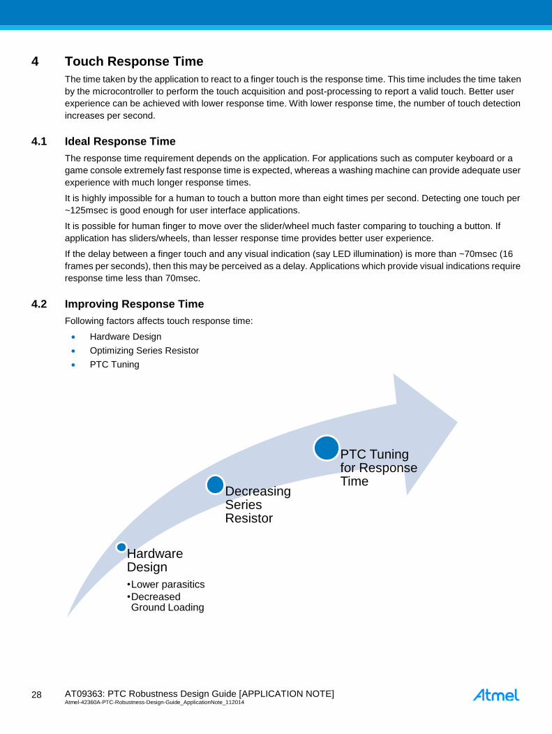
4 Touch Response Time ........................................................................................................... 28
4.1 Ideal Response Time ......................................................................................................................................... 28
4.2 Improving Response Time ................................................................................................................................. 28
4.2.1 Hardware Design ................................................................................................................................... 29
4.2.2 Optimizing Series Resistor .................................................................................................................... 29
4.2.3 Increasing CPU Clock ........................................................................................................................... 29
4.2.4 PTC Tuning for Response Time ............................................................................................................ 29
5 Reference ................................................................................................................................ 31
6 Revision History ..................................................................................................................... 32
Page 4
AT09363: PTC Robustness Design Guide [APPLICATION NOTE] Atmel-42360A-PTC-Robustness-Design-Guide_ApplicationNote_112014
3
3
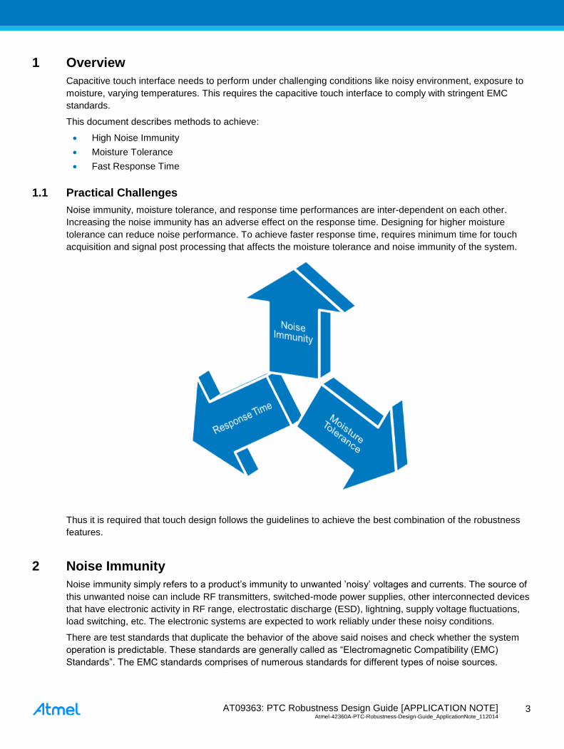
1 Overview
Capacitive touch interface needs to perform under challenging conditions like noisy environment, exposure to
moisture, varying temperatures. This requires the capacitive touch interface to comply with stringent EMC
standards.
This document describes methods to achieve:
High Noise Immunity
Moisture Tolerance
Fast Response Time
1.1 Practical Challenges
Noise immunity, moisture tolerance, and response time performances are inter-dependent on each other.
Increasing the noise immunity has an adverse effect on the response time. Designing for higher moisture
tolerance can reduce noise performance. To achieve faster response time, requires minimum time for touch
acquisition and signal post processing that affects the moisture tolerance and noise immunity of the system.
Thus it is required that touch design follows the guidelines to achieve the best combination of the robustness
features.
2 Noise Immunity
Noise immunity simply refers to a product’s immunity to unwanted ’noisy’ voltages and currents. The source of
this unwanted noise can include RF transmitters, switched-mode power supplies, other interconnected devices
that have electronic activity in RF range, electrostatic discharge (ESD), lightning, supply voltage fluctuations,
load switching, etc. The electronic systems are expected to work reliably under these noisy conditions.
There are test standards that duplicate the behavior of the above said noises and check whether the system
operation is predictable. These standards are generally called as “Electromagnetic Compatibility (EMC)
Standards”. The EMC standards comprises of numerous standards for different types of noise sources.
Page 5
AT09363: PTC Robustness Design Guide [APPLICATION NOTE] Atmel-42360A-PTC-Robustness-Design-Guide_ApplicationNote_112014 4
4
2.1 EMC Standards
This section provides an overview of few typical EMC test standards to which capacitive touch interfaces are
subjected.
2.1.1 IEC 61000-4-2 – Immunity to Electrostatic Discharge (ESD)
ESD refers to a sudden flow of current between two charged object due to static electricity. In general this current
is very high and can cause permanent damage to the microcontroller. The main sources of ESD are
plug-and-play electronic devices, human contact, etc.
In general, touch applications are touched through a touch panel which is made of dielectric material. So, the
touch applications are inherently protected from ESD. Some special attention should be given if the expected
ESD stress level is more than the breakdown voltage of the touch panel or if the circuitry is not completely
covered by the enclosure.
2.1.2 IEC 61000-4-4 – Immunity to Electrical Fast Transients (EFT)
EFT occurs when a gaseous discharge occurs when opening a switch through which current was flowing. The
effect of the transient discharge is huge if the conductor was carrying huge amount of current. The EFT couples
with the cables which are closer in proximity and travels on the line until it finds a discharge path.
This charge lasts only for a short duration (in the order of few nanoseconds (ns)). Touch applications are
expected to operate normally without any false detect during the test.
2.1.3 IEC 61000-4-5 – Immunity to Surge Voltage
Enormous amount of charge gets formed on the transmission lines when lightning hits transmission lines. This
charge gets distributed throughout the line and redirected to earth at various stages. There are cases where this
charge is observed even on the main supply of houses. The amount of charge is huge and it is equivalent to a few
Kilo-Voltage (KV). Similar kind of charge (with lesser amplitude) gets formed on the lines when huge load is
disconnected from the supply in industries or in power-grids.
The charge takes time, in the order of few micro-seconds (µs) to get discharged. Touch applications are
expected to operate normally without any false detect during the test.
2.1.4 IEC 61000-4-6 – Immunity to Conducted Disturbances
Conducted noise will generally be in common-mode (CM) and appear across all connecting cables to a device.
Capacitive touch applications are generally not affected by CM noise until human interaction takes place. This is
because the power supply lines maintain a stable difference between VDD and GND and as no return path is
provided to the noise source reference(usually EARTH), the circuit functions normally.
Once human interaction takes place, however, the user’s finger now provides a return path and effectively
couples noise directly into the capacitive sensor. When this noise reaches levels where normal filtering
algorithms become ineffective, errors are introduced into the touch acquisition and the system becomes
unreliable. This can manifest itself by way of no touch detect, false detect or in some cases, a complete system
lock-up.
2.2 Improving Noise Immunity
To apply suitable techniques and address the effects of unwanted noise disturbances, it is important to
understand the environment in which the touch application needs to operate. The noise immunity of a system can
be increased significantly by complying with the recommended guidelines throughout the different phases of a
design cycle.
Page 6
AT09363: PTC Robustness Design Guide [APPLICATION NOTE] Atmel-42360A-PTC-Robustness-Design-Guide_ApplicationNote_112014
5
5
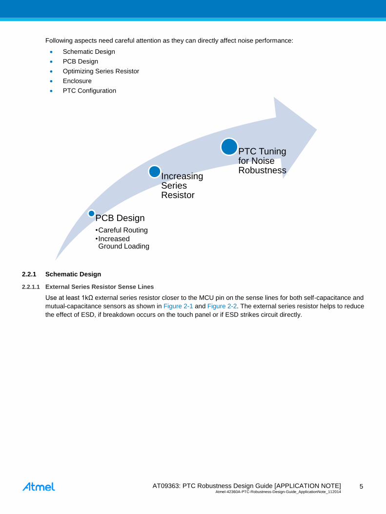
Following aspects need careful attention as they can directly affect noise performance:
Schematic Design
PCB Design
Optimizing Series Resistor
Enclosure
PTC Configuration
2.2.1 Schematic Design
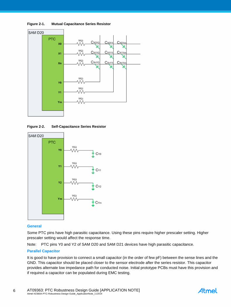
2.2.1.1 External Series Resistor Sense Lines
Use at least 1kΩ external series resistor closer to the MCU pin on the sense lines for both self-capacitance and
mutual-capacitance sensors as shown in Figure 2-1 and Figure 2-2. The external series resistor helps to reduce
the effect of ESD, if breakdown occurs on the touch panel or if ESD strikes circuit directly.
PCB Design
•Careful Routing
•Increased Ground Loading
Increasing Series Resistor
PTC Tuning for Noise Robustness
Page 7
AT09363: PTC Robustness Design Guide [APPLICATION NOTE] Atmel-42360A-PTC-Robustness-Design-Guide_ApplicationNote_112014 6
6
Figure 2-1. Mutual Capacitance Series Resistor
Figure 2-2. Self-Capacitance Series Resistor
General
Some PTC pins have high parasitic capacitance. Using these pins require higher prescaler setting. Higher
prescaler setting would affect the response time.
Note: PTC pins Y0 and Y2 of SAM D20 and SAM D21 devices have high parasitic capacitance.
Parallel Capacitor
It is good to have provision to connect a small capacitor (in the order of few pF) between the sense lines and the
GND. This capacitor should be placed closer to the sensor electrode after the series resistor. This capacitor
provides alternate low impedance path for conducted noise. Initial prototype PCBs must have this provision and
if required a capacitor can be populated during EMC testing.
Page 8
AT09363: PTC Robustness Design Guide [APPLICATION NOTE] Atmel-42360A-PTC-Robustness-Design-Guide_ApplicationNote_112014
7
7
Dedicated Voltage Regulator
It is recommended to use dedicated voltage regulator for higher noise immunity. Use linear voltage regulator
preferably as it generates lesser noise compared to switching regulator. Ripple on the regulator output should be
less than ±5% of supply voltage. If the design intends to use same voltage regulator for all circuit, then initial
prototype PCBs must have provision to connect a dedicated voltage regulator to MCU. This provision can be
used during various performance testing.
Decoupling Capacitor
Ensure that all the VDD lines of MCU have at least one dedicated decoupling capacitor. Using three capacitors,
1µF, 100nF, and 1nF on each VDD line reduces effect of different frequency band noises.
Series Resistor on VDD Lines
Include a series resistor (10Ω) or ferrite bead, between the regulator and VDD pin(s) of the MCU. This reduces
the effect of EFT/Surge on the MCU.
Bulk Capacitor
Use bulk capacitors closer to the voltage regulator. Refer to the voltage regulator datasheet which specifies the
typical value and type of the recommended capacitors.
Use 10µF bulk capacitor on VDD line closer to MCU under following conditions.
If separate plane for VDD is not available
If MCU is placed at a distance more than 10cm from voltage regulator
If output of the voltage regulator is shared with other circuitry
If voltage regulator and MCU are placed on different PCBs
Ensure that the shunt capacitor’s voltage rating is more (in the order of KV) if it is used before EFT suppressor.
Otherwise the capacitor can break.
Transient Voltage Suppressors (TVS) Diodes
If the system is expected to operate under high level of ESDs, Transient Voltage Suppressors (TVS) diodes can
be used on the sense lines. Ensure that the TVS diodes are placed closer to the area where ESD strike can occur
(in most cases it is sensor electrode).
If TVS diodes are used on sense lines ensure that the capacitance of the same less than 1pF.
Metal-Oxide Varistors (MOV)
Mains powered applications are likely to suffer due to high voltage surges. MOVs are required to protect the
circuit from high voltage surges. Surge voltage varies depending on geographical location. MOVs should be
selected based on the geographical location where the application is intended to operate.
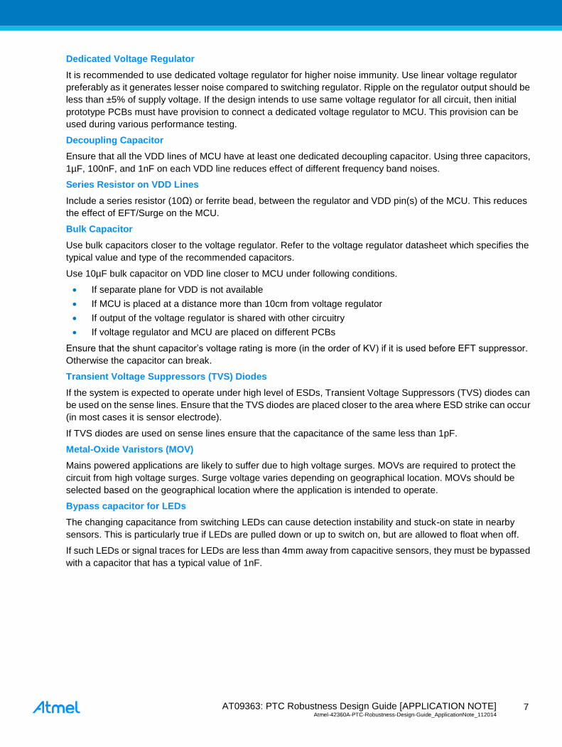
Bypass capacitor for LEDs
The changing capacitance from switching LEDs can cause detection instability and stuck-on state in nearby
sensors. This is particularly true if LEDs are pulled down or up to switch on, but are allowed to float when off.
If such LEDs or signal traces for LEDs are less than 4mm away from capacitive sensors, they must be bypassed
with a capacitor that has a typical value of 1nF.
Page 9
AT09363: PTC Robustness Design Guide [APPLICATION NOTE] Atmel-42360A-PTC-Robustness-Design-Guide_ApplicationNote_112014 8
8
Figure 2-3. Bypass Capacitor for Nearby LEDs
2.2.2 PCB Design
2.2.2.1 Sensor Design
Ensure parasitic capacitance of the sensor including the electrode and sensor traces, is not more than 30pF. In
case of Sliders/Wheels, the parasitic capacitance of each channel should not be more than 30pF.
The “Compensation Capacitance (CC)” calibration value can be used to find whether the parasitic capacitance is
high. If CC calibration value of a channel is greater than or equal to 16383, then the parasitic capacitance of that
channel is more than 30pF.
For additional details on how to read the CC calibration value refer to Atmel® QTouch
® Library Peripheral Touch
Controller User Guide[3]
.
For additional details on the sensor design refer to QTAN0079 Buttons, Sliders and Wheels Sensor Design
Guide[1]
.
2.2.2.2 Layout Considerations
Sensor Placement
It is better to group the sensor electrodes to one side of the panel. Placing sensors randomly in the panel will
result in unequal parasitic capacitance. To ensure that the sensor electrode which has highest parasitic
capacitance is fully charged, the prescaler setting needs to be increased which affects response time. Grouping
the sensors on the panel can help in achieving better moisture tolerance.
Noise Sources
If high noise generating components, like, relays, crystal oscillator, inductor, switching regulator, etc, are used
ensure that they are properly isolated from the touch circuitry.
Stacked PCB Design
In stacked PCB design, ensure that the noise from the other PCB does not affect touch circuitry by properly
providing physical gap. In case physical gap is not possible, it is recommended to use a ground plane to isolate
the noise from the other PCB.
Enough Space on Edges
Avoid placing touch sensors close to the edges of the PCB. It is recommended to provide enough clearance
between the PCB edge and the sensor electrode. Use of ground traces routed on the PCB edges helps to
improve noise immunity.
Page 10
AT09363: PTC Robustness Design Guide [APPLICATION NOTE] Atmel-42360A-PTC-Robustness-Design-Guide_ApplicationNote_112014
9
9
Discrete
Ensure that the series resistors of sense traces are placed close to the MCU pin
If series resistors are used for VDD lines, ensure that they are placed closer to the MCU pin
Ensure that pull-up resistor and de-coupling capacitor for RESET line are placed closer to the MCU pin
Ensure that the de-coupling capacitors are placed closer to the VDD pin
Ensure that TVS diodes are placed closer to noise source to ensure that a surge voltage is clamped before
the pulse is coupled into adjacent PCB traces
2.2.2.3 Routing
Shorter Sensor Traces
Traces from the microcontroller pins to the sensor electrode should be as short as possible. Making long traces
increases loading on the sense line. In practice, using protection mechanism (say ground shielding) is easy to
make in short traces comparing to that of longer traces.
Thinner Traces
To prevent false touches over sensor traces keep trace width between 0.1mm and 0.5mm. The sensor traces
should be routed on the non-touch side and should be connected to the sensor electrode preferably through a
PCB via. This makes the sense traces insensitive to finger touch.
Nearby Traces
Sense traces should not be placed near other traces and components, as this may cause loading and
interference. Longer sense traces will load the sensor and reduce the sensitivity. Traces with switching
signals that are placed close to the sense traces can cause noise in sensors.
GND traces should not be placed near sense traces. This will load the sensor and reduce the sensitivity.
To reduce loading the sense traces and GND traces should cross at 90° on separate layers. If shielding
from noise sources is necessary a thin meshed ground may be used behind electrodes (<40% copper).
Meshed ground can also be helpful in increasing SNR.
X and Y Traces
For mutual-capacitance, PTC X- and Y-lines should not be routed for longer length. Combination of that X and Y
forms a channel and trace area becomes sensitive to touch. It is better to group the X traces together and Y
traces together and route them physically separated on the PCB.
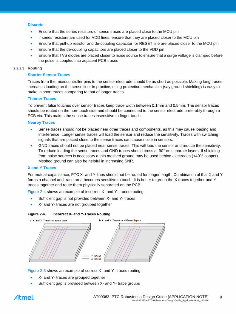
Figure 2-4 shows an example of incorrect X- and Y- traces routing.
Sufficient gap is not provided between X- and Y- traces
X- and Y- traces are not grouped together
Figure 2-4. Incorrect X- and Y-Traces Routing
Figure 2-5 shows an example of correct X- and Y- traces routing.
X- and Y- traces are grouped together
Sufficient gap is provided between X- and Y- trace groups
Page 11
AT09363: PTC Robustness Design Guide [APPLICATION NOTE] Atmel-42360A-PTC-Robustness-Design-Guide_ApplicationNote_112014 1
0
10
Figure 2-5. Correct X- and Y-Traces Routing – Example 1
Figure 2-6 shows an example of correct X- and Y- traces routing.
X- and Y- traces are grouped together
Not able to provide sufficient gap between X- and Y- trace groups. So, a ground trace is routed between X-
and Y- trace groups
Figure 2-6. Correct X- and Y-Traces Routing – Example 2
Ground Shield
In all layers GND trace/plane should surround all other signal traces. This can be achieved by placing thick
ground trace on the edges of the PCB on all layers. Alternatively copper pour can be used in empty space of the
PCB and can be connected to GND. The GND trace acts as a barrier between noise and the signal. Using
“stitching vias” located closer to each other on the edge of the PCB helps in reducing the effect of noise even
from the sides of the PCB.
Note: Having ground plane surrounding the sensor electrode reduces moisture tolerance. A compromise
between noise reduction and moisture tolerance can be achieved by providing a gap of 3-5mm between
sensor electrode and ground plane.
2.2.2.4 Improve Return Path (Ground Plane)
Additional improvements in noise immunity can be achieved by providing better return path. This can be in the
form of a ground flood on the same plane or as a meshed ground plane behind the sensor. The ground fill
provides a low impedance path for the noise, directing it away from the MCUs input pins. Effective return path
can be achieved using “stitching vias” to connect ground fill on multiple layers of a PCB.
In multi-board systems, the ground connections between boards should be made via multiple pins. The multiple
pins should be spread across the board to avoid longer return path. This can be achieved by connecting the
mounting holes to ground plane and use conductive screws.
Page 12
AT09363: PTC Robustness Design Guide [APPLICATION NOTE] Atmel-42360A-PTC-Robustness-Design-Guide_ApplicationNote_112014
11
11
Although adding ground plane reduces sensitivity, the improvement in SNR is much more significant when
operating in noisy environments. In most cases, loss of sensitivity due to ground loading can be compensated by
adjusting the Gain setting or Detect Threshold.
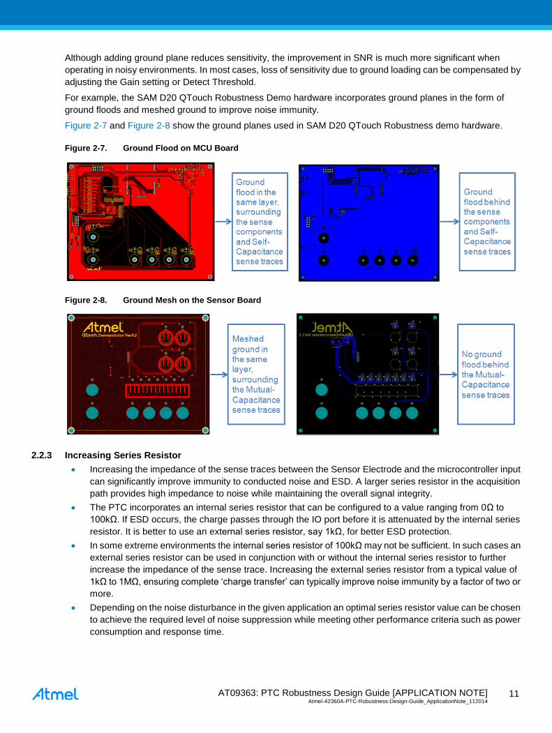
For example, the SAM D20 QTouch Robustness Demo hardware incorporates ground planes in the form of
ground floods and meshed ground to improve noise immunity.
Figure 2-7 and Figure 2-8 show the ground planes used in SAM D20 QTouch Robustness demo hardware.
Figure 2-7. Ground Flood on MCU Board
Figure 2-8. Ground Mesh on the Sensor Board
2.2.3 Increasing Series Resistor
Increasing the impedance of the sense traces between the Sensor Electrode and the microcontroller input
can significantly improve immunity to conducted noise and ESD. A larger series resistor in the acquisition
path provides high impedance to noise while maintaining the overall signal integrity.
The PTC incorporates an internal series resistor that can be configured to a value ranging from 0Ω to
100kΩ. If ESD occurs, the charge passes through the IO port before it is attenuated by the internal series
resistor. It is better to use an external series resistor, say 1kΩ, for better ESD protection.
In some extreme environments the internal series resistor of 100kΩ may not be sufficient. In such cases an
external series resistor can be used in conjunction with or without the internal series resistor to further
increase the impedance of the sense trace. Increasing the external series resistor from a typical value of
1kΩ to 1MΩ, ensuring complete ‘charge transfer’ can typically improve noise immunity by a factor of two or
more.
Depending on the noise disturbance in the given application an optimal series resistor value can be chosen
to achieve the required level of noise suppression while meeting other performance criteria such as power
consumption and response time.
Page 13
AT09363: PTC Robustness Design Guide [APPLICATION NOTE] Atmel-42360A-PTC-Robustness-Design-Guide_ApplicationNote_112014 1
2
12
For example, in SAM D20 QTouch Robustness Demo the self-capacitance sensors use an external series
resistor of 220kΩ in order to pass CI testing at 10V. No internal series resistor was used. In self-capacitance,
using external series resistor is more effective comparing to internal series resistor.
The mutual-capacitance sensors are able to pass CI testing at 10V with an internal series resistor of 100kΩ. An
external series resistor of 1kΩ is used for ESD protection.
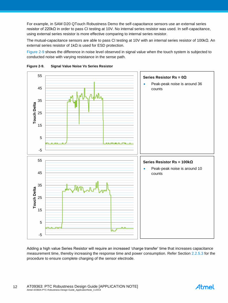
Figure 2-9 shows the difference in noise level observed in signal value when the touch system is subjected to
conducted noise with varying resistance in the sense path.
Figure 2-9. Signal Value Noise Vs Series Resistor
Adding a high value Series Resistor will require an increased ‘charge transfer’ time that increases capacitance
measurement time, thereby increasing the response time and power consumption. Refer Section 2.2.5.3 for the
procedure to ensure complete charging of the sensor electrode.
-5
5
15
25
35
45
55
To
uch
Delt
a
-5
5
15
25
35
45
55
To
uch
Delt
a
Series Resistor Rs = 100kΩ
Peak-peak noise is around 10
counts
Series Resistor Rs = 0Ω
Peak-peak noise is around 36
counts
Page 14
AT09363: PTC Robustness Design Guide [APPLICATION NOTE] Atmel-42360A-PTC-Robustness-Design-Guide_ApplicationNote_112014
13
13
2.2.4 Enclosure
Designing a proper enclosure can help in improving ESD performance. In most application glass/acrylic is used
as touch panel over the touch user interface and plastic as the enclosure for other parts.
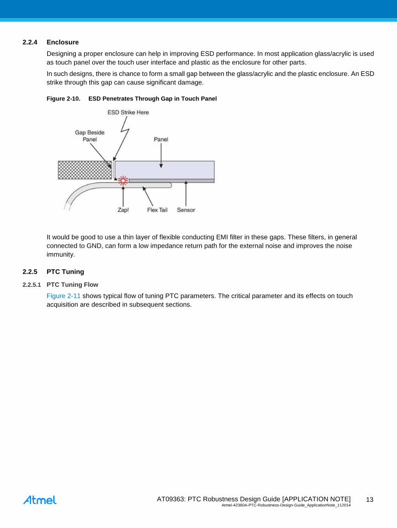
In such designs, there is chance to form a small gap between the glass/acrylic and the plastic enclosure. An ESD
strike through this gap can cause significant damage.
Figure 2-10. ESD Penetrates Through Gap in Touch Panel
It would be good to use a thin layer of flexible conducting EMI filter in these gaps. These filters, in general
connected to GND, can form a low impedance return path for the external noise and improves the noise
immunity.
2.2.5 PTC Tuning
2.2.5.1 PTC Tuning Flow
Figure 2-11 shows typical flow of tuning PTC parameters. The critical parameter and its effects on touch
acquisition are described in subsequent sections.
Page 15
AT09363: PTC Robustness Design Guide [APPLICATION NOTE] Atmel-42360A-PTC-Robustness-Design-Guide_ApplicationNote_112014 1
4
14
Figure 2-11. PTC Tuning Flow Chart
Page 16
AT09363: PTC Robustness Design Guide [APPLICATION NOTE] Atmel-42360A-PTC-Robustness-Design-Guide_ApplicationNote_112014
15
15
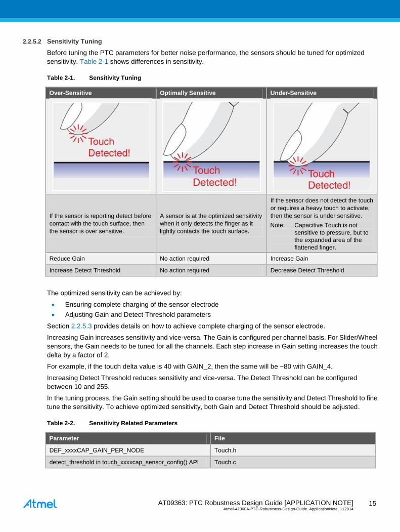
2.2.5.2 Sensitivity Tuning
Before tuning the PTC parameters for better noise performance, the sensors should be tuned for optimized
sensitivity. Table 2-1 shows differences in sensitivity.
Table 2-1. Sensitivity Tuning
Over-Sensitive Optimally Sensitive Under-Sensitive
If the sensor is reporting detect before
contact with the touch surface, then
the sensor is over sensitive.
A sensor is at the optimized sensitivity
when it only detects the finger as it
lightly contacts the touch surface.
If the sensor does not detect the touch
or requires a heavy touch to activate,
then the sensor is under sensitive.
Note: Capacitive Touch is not
sensitive to pressure, but to
the expanded area of the
flattened finger.
Reduce Gain No action required Increase Gain
Increase Detect Threshold No action required Decrease Detect Threshold
The optimized sensitivity can be achieved by:
Ensuring complete charging of the sensor electrode
Adjusting Gain and Detect Threshold parameters
Section 2.2.5.3 provides details on how to achieve complete charging of the sensor electrode.
Increasing Gain increases sensitivity and vice-versa. The Gain is configured per channel basis. For Slider/Wheel
sensors, the Gain needs to be tuned for all the channels. Each step increase in Gain setting increases the touch
delta by a factor of 2.
For example, if the touch delta value is 40 with GAIN_2, then the same will be ~80 with GAIN_4.
Increasing Detect Threshold reduces sensitivity and vice-versa. The Detect Threshold can be configured
between 10 and 255.
In the tuning process, the Gain setting should be used to coarse tune the sensitivity and Detect Threshold to fine
tune the sensitivity. To achieve optimized sensitivity, both Gain and Detect Threshold should be adjusted.
Table 2-2. Sensitivity Related Parameters
Parameter File
DEF_xxxxCAP_GAIN_PER_NODE Touch.h
detect_threshold in touch_xxxxcap_sensor_config() API Touch.c
Page 17
AT09363: PTC Robustness Design Guide [APPLICATION NOTE] Atmel-42360A-PTC-Robustness-Design-Guide_ApplicationNote_112014 1
6
16
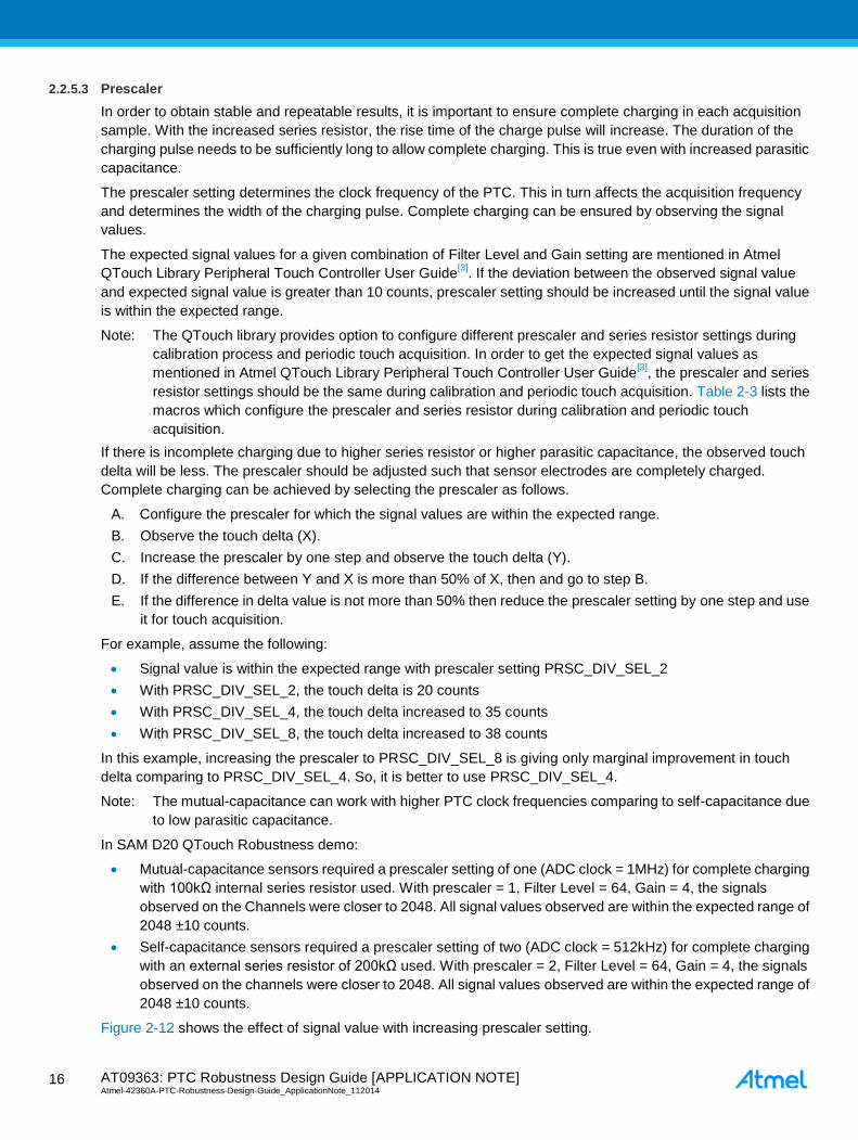
2.2.5.3 Prescaler
In order to obtain stable and repeatable results, it is important to ensure complete charging in each acquisition
sample. With the increased series resistor, the rise time of the charge pulse will increase. The duration of the
charging pulse needs to be sufficiently long to allow complete charging. This is true even with increased parasitic
capacitance.
The prescaler setting determines the clock frequency of the PTC. This in turn affects the acquisition frequency
and determines the width of the charging pulse. Complete charging can be ensured by observing the signal
values.
The expected signal values for a given combination of Filter Level and Gain setting are mentioned in Atmel
QTouch Library Peripheral Touch Controller User Guide[3]
. If the deviation between the observed signal value
and expected signal value is greater than 10 counts, prescaler setting should be increased until the signal value
is within the expected range.
Note: The QTouch library provides option to configure different prescaler and series resistor settings during
calibration process and periodic touch acquisition. In order to get the expected signal values as
mentioned in Atmel QTouch Library Peripheral Touch Controller User Guide[3]
, the prescaler and series
resistor settings should be the same during calibration and periodic touch acquisition. Table 2-3 lists the
macros which configure the prescaler and series resistor during calibration and periodic touch
acquisition.
If there is incomplete charging due to higher series resistor or higher parasitic capacitance, the observed touch
delta will be less. The prescaler should be adjusted such that sensor electrodes are completely charged.
Complete charging can be achieved by selecting the prescaler as follows.
A. Configure the prescaler for which the signal values are within the expected range.
B. Observe the touch delta (X).
C. Increase the prescaler by one step and observe the touch delta (Y).
D. If the difference between Y and X is more than 50% of X, then and go to step B.
E. If the difference in delta value is not more than 50% then reduce the prescaler setting by one step and use
it for touch acquisition.
For example, assume the following:
Signal value is within the expected range with prescaler setting PRSC_DIV_SEL_2
With PRSC_DIV_SEL_2, the touch delta is 20 counts
With PRSC_DIV_SEL_4, the touch delta increased to 35 counts
With PRSC_DIV_SEL_8, the touch delta increased to 38 counts
In this example, increasing the prescaler to PRSC_DIV_SEL_8 is giving only marginal improvement in touch
delta comparing to PRSC_DIV_SEL_4. So, it is better to use PRSC_DIV_SEL_4.
Note: The mutual-capacitance can work with higher PTC clock frequencies comparing to self-capacitance due
to low parasitic capacitance.
In SAM D20 QTouch Robustness demo:
Mutual-capacitance sensors required a prescaler setting of one (ADC clock = 1MHz) for complete charging
with 100kΩ internal series resistor used. With prescaler = 1, Filter Level = 64, Gain = 4, the signals
observed on the Channels were closer to 2048. All signal values observed are within the expected range of
2048 ±10 counts.
Self-capacitance sensors required a prescaler setting of two (ADC clock = 512kHz) for complete charging
with an external series resistor of 200kΩ used. With prescaler = 2, Filter Level = 64, Gain = 4, the signals
observed on the channels were closer to 2048. All signal values observed are within the expected range of
2048 ±10 counts.
Figure 2-12 shows the effect of signal value with increasing prescaler setting.
Page 18
AT09363: PTC Robustness Design Guide [APPLICATION NOTE] Atmel-42360A-PTC-Robustness-Design-Guide_ApplicationNote_112014
17
17
Figure 2-12. Signal Value Noise Vs Prescaler
Table 2-3. Prescaler Related Parameters
Parameter File
DEF_xxxxCAP_CC_CAL_CLK_PRESCALE Touch.c
DEF_xxxxCAP_CC_CAL_SENSE_RESISTOR Touch.c
DEF_xxxxCAP_CLK_PRESCALE Touch.h
DEF_xxxxCAP_SENSE_RESISTOR Touch.h
2.2.5.4 Filter Level
The QTouch library provides the option to do over-sampling and averaging. The averaging acts as low-pass filter
and reduce the noise level significantly. “DEF_xxxxCAP_FILTER_LEVEL” parameter defined in touch.h file
determines the over-sample counts. More information on this parameter can be found in Atmel QTouch Library
Peripheral Touch Controller User Guide[3]
.
2030
2040
2050
2060
2070
2080
2090
2100
2110 S
ign
al L
ev
el
2030
2040
2050
2060
2070
2080
2090
2100
2110
Sig
nal L
ev
el
Prescaler = 2
The signal values of all the
channels are closer to the expected
signal value (2048).
Touch delta values observed are
more compared to that with
prescaler set to 1.
Prescaler = 1
Deviation between expected signal
value (2048) and actual signal
value. This is marked by a red
circle.
Touch delta values are not even on
all channels and few channels
show lower touch delta values.
Page 19
AT09363: PTC Robustness Design Guide [APPLICATION NOTE] Atmel-42360A-PTC-Robustness-Design-Guide_ApplicationNote_112014 1
8
18
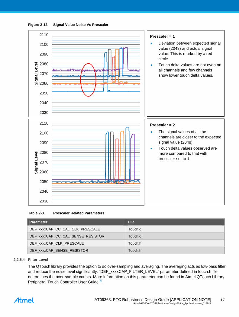
Figure 2-13 shows the difference in signal variation of a self-capacitance sensor with respect to change in filter
level.
Figure 2-13. Signal Value Noise Vs Filter Level
Table 2-4. Filter Level Related Parameter
Parameter File
DEF_xxxxCAP_FILTER_LEVEL Touch.h
2.2.5.5 Frequency Mode
The noise level on the signal value increases if the frequency of the noise is closer to the touch acquisition
frequency. If increasing the filter level is not helping in reducing the noise level, then it is better to change the
acquisition frequency. QTouch library provides an option to perform touch acquisition on three different
frequencies. “DEF_xxxxCAP_FREQ_MODE” parameter defined in touch.h file determines mode used by the
QTouch library for touch acquisition. “FREQ_MODE_HOP” mode uses three frequencies to perform touch
2044
2046
2048
2050
2052
2054
2056
2058
Sig
nal L
ev
el
2044
2046
2048
2050
2052
2054
2056
2058
Sig
nal L
ev
el
Filter Level = 64
The peak-to-peak signal variation is
six counts. This is almost half
compared to that of filter level 32.
Filter Level = 32
The peak-to-peak signal variation is
11 counts
Page 20
AT09363: PTC Robustness Design Guide [APPLICATION NOTE] Atmel-42360A-PTC-Robustness-Design-Guide_ApplicationNote_112014
19
19
acquisition and applies median filter on the resulting three signal values. The user can configure the frequencies
on which the QTouch library performs touch acquisition. The user can select three frequencies from a list of
sixteen frequencies using “DEF_MUTLCAP_HOP_FREQS” parameter in touch.h file.
More information on these parameters can be found in Atmel QTouch Library Peripheral Touch Controller User
Guide[3]
.
Combination of three different frequencies and median filter helps in eliminating the noise level in most of the
cases. To identify the correct frequencies for a given system, user needs to iterate with different combination of
frequencies and select the best possible combination that show less noise levels. Better noise rejection can be
achieved by using combination of spread-apart frequencies. For example, combination of frequencies 2, 4, and 8
will reject noise better comparing to combination of frequencies 4, 5, and 6.
Figure 2-14 shows the effect of noise on delta value between “FREQ_MODE_NONE” and
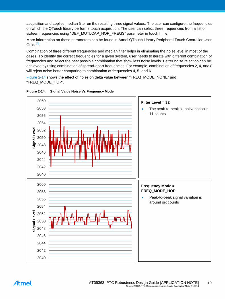
“FREQ_MODE_HOP”.
Figure 2-14. Signal Value Noise Vs Frequency Mode
2040
2042
2044
2046
2048
2050
2052
2054
2056
2058
2060
Sig
nal L
ev
el
2040
2042
2044
2046
2048
2050
2052
2054
2056
2058
2060
Sig
nal L
ev
el
Frequency Mode =
FREQ_MODE_HOP
Peak-to-peak signal variation is
around six counts
Filter Level = 32
The peak-to-peak signal variation is
11 counts
Page 21
AT09363: PTC Robustness Design Guide [APPLICATION NOTE] Atmel-42360A-PTC-Robustness-Design-Guide_ApplicationNote_112014 2
0
20
Table 2-5. Frequency Mode Related Parameters
Parameter File
DEF_xxxxCAP_FREQ_MODE Touch.h
DEF_xxxxCAP_HOP_FREQS Touch.h
2.2.5.6 Frequency Auto Tune
Frequency auto tune is an advanced feature provided by QTouch Library. This feature measures the noise on the
frequencies used in “FREQ_MODE_HOP” and dynamically replaces the nosiest frequency. This feature is
helpful if the system is subjected to different noises of varying frequencies. The frequency switch happens if the
signal value is unstable and exceeds the stability limit consistently for auto tune count times.
“DEF_xxxxCAP_FREQ_AUTO_TUNE_SIGNAL_STABILITY_LIMIT” sets the stability limit and
“DEF_xxxxCAP_FREQ_AUTO_TUNE_IN_CNT” sets the auto tune count.
More information on these parameters can be found in Atmel QTouch Library Peripheral Touch Controller User
Guide[3]
.
Note: The frequency auto tune feature is applicable only if “FREQ_MODE_HOP” frequency mode is used.
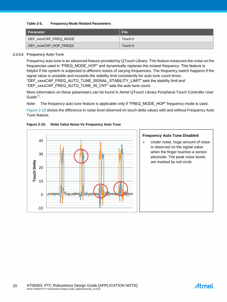
Figure 2-15 shows the difference in noise level observed on touch delta values with and without Frequency Auto
Tune feature.
Figure 2-15. Delta Value Noise Vs Frequency Auto Tune
-10
0
10
20
30
40
To
uch
Delt
a
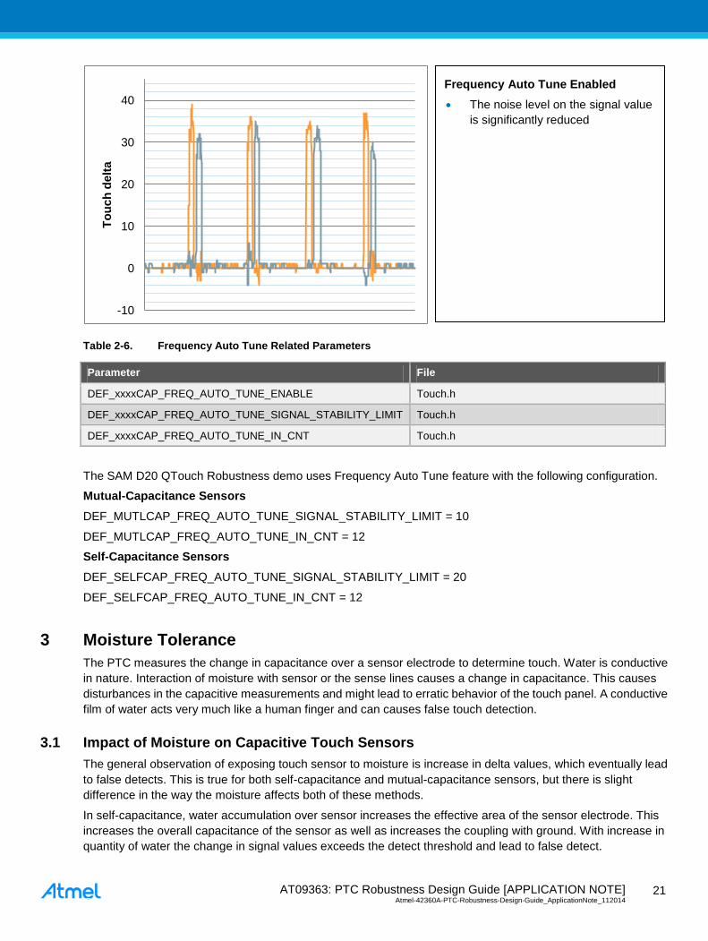
Frequency Auto Tune Disabled
Under noise, huge amount of noise
is observed on the signal value
when the finger touches a sensor
electrode. The peak noise levels
are marked by red circle.
Page 22
AT09363: PTC Robustness Design Guide [APPLICATION NOTE] Atmel-42360A-PTC-Robustness-Design-Guide_ApplicationNote_112014
21
21
Table 2-6. Frequency Auto Tune Related Parameters
Parameter File
DEF_xxxxCAP_FREQ_AUTO_TUNE_ENABLE Touch.h
DEF_xxxxCAP_FREQ_AUTO_TUNE_SIGNAL_STABILITY_LIMIT Touch.h
DEF_xxxxCAP_FREQ_AUTO_TUNE_IN_CNT Touch.h
The SAM D20 QTouch Robustness demo uses Frequency Auto Tune feature with the following configuration.
Mutual-Capacitance Sensors
DEF_MUTLCAP_FREQ_AUTO_TUNE_SIGNAL_STABILITY_LIMIT = 10
DEF_MUTLCAP_FREQ_AUTO_TUNE_IN_CNT = 12
Self-Capacitance Sensors
DEF_SELFCAP_FREQ_AUTO_TUNE_SIGNAL_STABILITY_LIMIT = 20
DEF_SELFCAP_FREQ_AUTO_TUNE_IN_CNT = 12
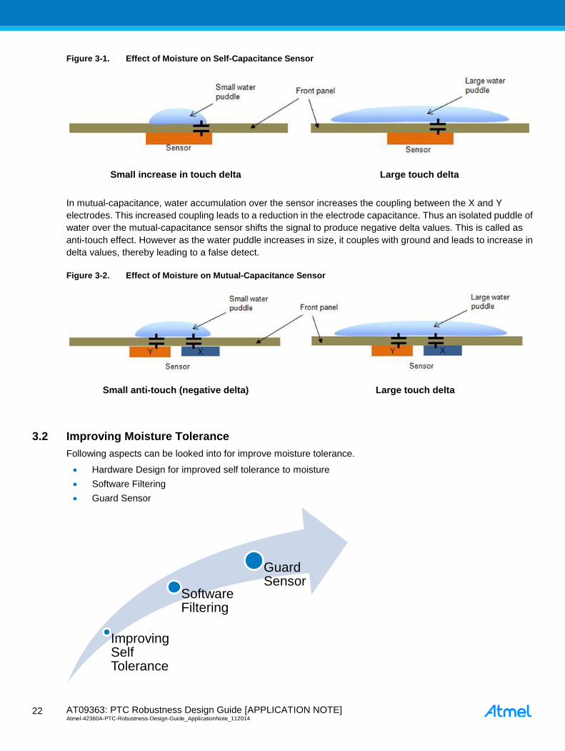
3 Moisture Tolerance
The PTC measures the change in capacitance over a sensor electrode to determine touch. Water is conductive
in nature. Interaction of moisture with sensor or the sense lines causes a change in capacitance. This causes
disturbances in the capacitive measurements and might lead to erratic behavior of the touch panel. A conductive
film of water acts very much like a human finger and can causes false touch detection.
3.1 Impact of Moisture on Capacitive Touch Sensors
The general observation of exposing touch sensor to moisture is increase in delta values, which eventually lead
to false detects. This is true for both self-capacitance and mutual-capacitance sensors, but there is slight
difference in the way the moisture affects both of these methods.
In self-capacitance, water accumulation over sensor increases the effective area of the sensor electrode. This
increases the overall capacitance of the sensor as well as increases the coupling with ground. With increase in
quantity of water the change in signal values exceeds the detect threshold and lead to false detect.
-10
0
10
20
30
40 T
ou
ch
delt
a
Frequency Auto Tune Enabled
The noise level on the signal value
is significantly reduced
Page 23
AT09363: PTC Robustness Design Guide [APPLICATION NOTE] Atmel-42360A-PTC-Robustness-Design-Guide_ApplicationNote_112014 2
2
22
Figure 3-1. Effect of Moisture on Self-Capacitance Sensor
In mutual-capacitance, water accumulation over the sensor increases the coupling between the X and Y
electrodes. This increased coupling leads to a reduction in the electrode capacitance. Thus an isolated puddle of
water over the mutual-capacitance sensor shifts the signal to produce negative delta values. This is called as
anti-touch effect. However as the water puddle increases in size, it couples with ground and leads to increase in
delta values, thereby leading to a false detect.
Figure 3-2. Effect of Moisture on Mutual-Capacitance Sensor
3.2 Improving Moisture Tolerance
Following aspects can be looked into for improve moisture tolerance.
Hardware Design for improved self tolerance to moisture
Software Filtering
Guard Sensor
Improving Self Tolerance
Software Filtering
Guard Sensor
Large touch delta Small anti-touch (negative delta)
Large touch delta Small increase in touch delta
Page 24
AT09363: PTC Robustness Design Guide [APPLICATION NOTE] Atmel-42360A-PTC-Robustness-Design-Guide_ApplicationNote_112014
23
23
3.2.1 Improving Self Tolerance
To improve the moisture tolerance of a touch panel, it is necessary to improve its self tolerance so that it can
reject a certain amount of moisture without any special implementations.
Selecting Touch Acquisition Method
– The mutual-capacitance sensors have a natural ability to reject moisture due to the anti-touch effect.
The use of mutual-capacitance sensors should be preferred in designs where moisture tolerance is a
concern. Water drops or small puddles can be handled by mutual-capacitance sensor design itself.
– Ground fill or other lines should be avoided near the sensor area. The ground plane offers very easy
path for water droplets to bridge and cause capacitive changes that appear similar to a normal touch.
– Reducing ground in the PCB decreases the overall noise immunity of the design. A careful
compromise has to be done.
Tune Detect Threshold
– The Detect Threshold should be kept as high as possible
Mechanical Design
When a touch panel is intended to work in conditions like water spill or rain, the below mechanical
recommendations should be considered.
– Mounting the touch panel at an inclined angle or vertically mounted is highly beneficial since it allows
the water to flow down and thereby prevents water accumulation on panel surface
– Size of sensor electrodes should not be made very large compared to fingers. A large sensor allows
more area for the moisture to interact and reduce the finger sensitivity.
– Use of concave touch panel surface above the sensor electrode instead of flat surfaces to avoid
water to stay on the button surface
3.2.2 Software Filtering
Avoiding false detects due to large water presence (or water flow) is very challenging. Software filter can be
implemented to monitor delta on all sensors and take appropriate measures based on the delta changes.
The idea is to ignore all touches in case there are ambiguous deltas on surrounding sensors and locks the panel
if surrounding sensors delta changes is high. This is helpful in case of sudden water spill on the touch panel as it
causes increase in delta on many sensors.
The use case for this filter depends on the nature of the application and the physical configuration of the sensors
on the touch panel. This is an effective solution for designs which have sensors spaced closer to each other and
requires minimal or no simultaneous touch detection on multiple sensors.
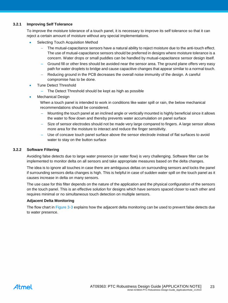
Adjacent Delta Monitoring
The flow chart in Figure 3-3 explains how the adjacent delta monitoring can be used to prevent false detects due
to water presence.
Page 25
AT09363: PTC Robustness Design Guide [APPLICATION NOTE] Atmel-42360A-PTC-Robustness-Design-Guide_ApplicationNote_112014 2
4
24
Figure 3-3. Flow Chart – Adjacent Delta Monitoring
The adjacent delta monitoring can be performed on a group of sensors that are physically closer to each other.
The above flow chart shows adjacent delta monitoring for one group. The same can be repeated for multiple
groups of sensors.
There may be condensation on PCB due to fast changes in the ambient temperature. This may cause larger
changes in capacitance on the sensor traces and causing false detects. Adjacent Delta Monitoring is an effective
solution to prevent false detects due to PCB condensation.
The SAM D20 QTouch Robustness demo uses adjacent delta monitoring technique to improve moisture
tolerance.
Figure 3-4 shows how the adjacent delta monitoring suppresses false detects during water spray over the touch
panel.
Page 26
AT09363: PTC Robustness Design Guide [APPLICATION NOTE] Atmel-42360A-PTC-Robustness-Design-Guide_ApplicationNote_112014
25
25
Figure 3-4. Effect of Water Spray Over the Touch Panel
The adjacent delta value increases as soon as the water is sprayed over the touch panel. The sensor states are
suppressed when adjacent delta value reaches the threshold (say 30 counts). With additional spraying, there is
further increase in adjacent delta. The panel is locked when adjacent delta reaches a value twice the threshold
(say 60 counts).
Figure 3-5 shows how the adjacent delta monitoring suppresses false detects when steam is applied over the
PCB.
Figure 3-5. Effect of Steam Over PCB
The adjacent delta value increases as soon as the steam is applied on the PCB. The sensor states are
suppressed when adjacent delta value reaches threshold (say 30 counts). With more steam, there is further
-10
10
30
50
70
90
110
To
uch
Delt
a
-10
10
30
50
70
90
110
130
To
uch
Delt
a
Start Spray
Threshold * 2
Threshold
Calculated
Adjacent Delta
Threshold
Threshold * 2
Apply Steam on PCB
Sensors are
recalibrated and
ready to touch
Calculated
Adjacent Delta
Page 27
AT09363: PTC Robustness Design Guide [APPLICATION NOTE] Atmel-42360A-PTC-Robustness-Design-Guide_ApplicationNote_112014 2
6
26
increase in adjacent delta. The panel is locked when adjacent delta value reaches a value twice the threshold
(say 60 counts).
When steam is removed, eventually water droplets from the PCB will evaporate and the delta reduces. When the
adjacent delta goes below the threshold (say 30 counts) the sensors are re-calibrated and the touch panel is
ready for normal operation.
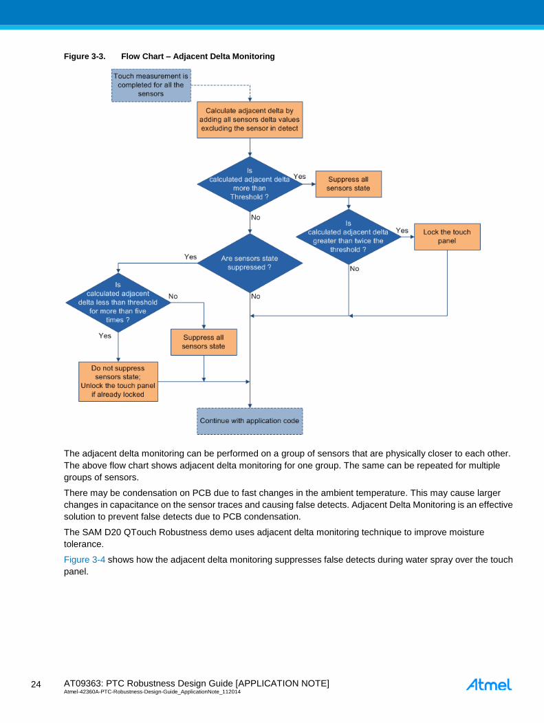
Figure 3-6 shows how the adjacent delta monitoring suppresses false detects when huge amount of water is
poured over the touch panel.
Figure 3-6. Water Pour Over Touch Panel
The adjacent delta value increases rapidly when huge amount of water is poured over the touch panel. The panel
is locked when adjacent delta value reaches two times the threshold (say 60 counts). When water is wiped, the
adjacent delta reduces and goes below the threshold (say 30 counts). The sensors are re-calibrated and the
touch panel is ready for normal operation.
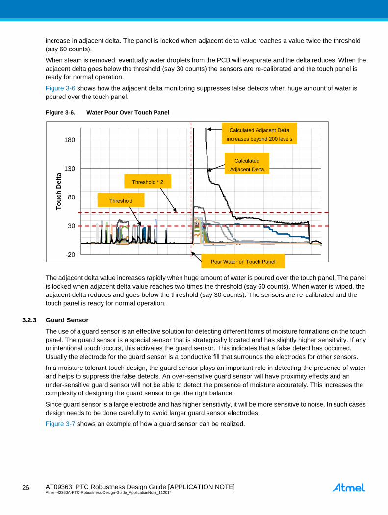
3.2.3 Guard Sensor
The use of a guard sensor is an effective solution for detecting different forms of moisture formations on the touch
panel. The guard sensor is a special sensor that is strategically located and has slightly higher sensitivity. If any
unintentional touch occurs, this activates the guard sensor. This indicates that a false detect has occurred.
Usually the electrode for the guard sensor is a conductive fill that surrounds the electrodes for other sensors.
In a moisture tolerant touch design, the guard sensor plays an important role in detecting the presence of water
and helps to suppress the false detects. An over-sensitive guard sensor will have proximity effects and an
under-sensitive guard sensor will not be able to detect the presence of moisture accurately. This increases the
complexity of designing the guard sensor to get the right balance.
Since guard sensor is a large electrode and has higher sensitivity, it will be more sensitive to noise. In such cases
design needs to be done carefully to avoid larger guard sensor electrodes.
Figure 3-7 shows an example of how a guard sensor can be realized.
-20
30
80
130
180
To
uch
Delt
a
Pour Water on Touch Panel
Threshold * 2
Threshold
Calculated
Adjacent Delta
Calculated Adjacent Delta
increases beyond 200 levels
Page 28
AT09363: PTC Robustness Design Guide [APPLICATION NOTE] Atmel-42360A-PTC-Robustness-Design-Guide_ApplicationNote_112014
27
27
Figure 3-7. Example Guard Sensor
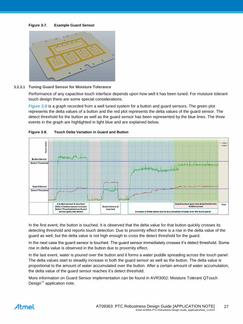
3.2.3.1 Tuning Guard Sensor for Moisture Tolerance
Performance of any capacitive touch interface depends upon how well it has been tuned. For moisture tolerant
touch design there are some special considerations.
Figure 3-8 is a graph recorded from a well tuned system for a button and guard sensors. The green plot
represents the delta values of a button and the red plot represents the delta values of the guard sensor. The
detect threshold for the button as well as the guard sensor has been represented by the blue lines. The three
events in the graph are highlighted in light blue and are explained below.
Figure 3-8. Touch Delta Variation in Guard and Button
In the first event, the button is touched. It is observed that the delta value for that button quickly crosses its
detecting threshold and reports touch detection. Due to proximity effect there is a rise in the delta value of the
guard as well, but the delta value is not high enough to cross the detect threshold for the guard.
In the next case the guard sensor is touched. The guard sensor immediately crosses it’s detect threshold. Some
rise in delta value is observed in the button due to proximity effect.
In the last event, water is poured over the button and it forms a water puddle spreading across the touch panel.
The delta values start to steadily increase in both the guard sensor as well as the button. The delta value is
proportional to the amount of water accumulated over the button. After a certain amount of water accumulation,
the delta value of the guard sensor reaches it’s detect threshold.
More information on Guard Sensor implementation can be found in AVR3002: Moisture Tolerant QTouch
Design[4]
application note.
Page 29
AT09363: PTC Robustness Design Guide [APPLICATION NOTE] Atmel-42360A-PTC-Robustness-Design-Guide_ApplicationNote_112014 2
8
28
4 Touch Response Time
The time taken by the application to react to a finger touch is the response time. This time includes the time taken
by the microcontroller to perform the touch acquisition and post-processing to report a valid touch. Better user
experience can be achieved with lower response time. With lower response time, the number of touch detection
increases per second.
4.1 Ideal Response Time
The response time requirement depends on the application. For applications such as computer keyboard or a
game console extremely fast response time is expected, whereas a washing machine can provide adequate user
experience with much longer response times.
It is highly impossible for a human to touch a button more than eight times per second. Detecting one touch per
~125msec is good enough for user interface applications.
It is possible for human finger to move over the slider/wheel much faster comparing to touching a button. If
application has sliders/wheels, than lesser response time provides better user experience.
If the delay between a finger touch and any visual indication (say LED illumination) is more than ~70msec (16
frames per seconds), then this may be perceived as a delay. Applications which provide visual indications require
response time less than 70msec.
4.2 Improving Response Time
Following factors affects touch response time:
Hardware Design
Optimizing Series Resistor
PTC Tuning
Hardware Design
•Lower parasitics
•Decreased Ground Loading
Decreasing Series Resistor
PTC Tuning for Response Time
Page 30
AT09363: PTC Robustness Design Guide [APPLICATION NOTE] Atmel-42360A-PTC-Robustness-Design-Guide_ApplicationNote_112014
29
29
4.2.1 Hardware Design
Increasing parasitic capacitance (Cp) increases touch acquisition time and vice-versa.
Parasitic Capacitance can be reduced as follows.
Reduce the trace length
– Longer sense traces running from the MCU to the sensor electrode increases the parasitic
capacitance
– In mutual-capacitance, avoid routing X- and Y -lines close to each other
Have a ground plane beneath the sensor electrode only if it is required
– Hatched ground flood can be used in low-noise systems
The size of the sensor electrode should be optimum
– Bigger sensors have higher parasitic capacitance. So, adequate sensor size should be used
– For spring based designs, it is recommended to use thinner wire gauge for springs. The pad size for
soldering the spring should be optimum to minimize the amount of solder.
4.2.2 Optimizing Series Resistor
Increasing Rs increases touch acquisition time and vice-versa. Select optimum Rs value for which system
performance is acceptable.
Avoid through-hole resistor as it increases parasitic capacitance.
4.2.3 Increasing CPU Clock
Increasing CPU clock frequency reduces post-processing time. CPU should be clocked at the maximum
clock frequency to get reduced response time and better user experience.
4.2.4 PTC Tuning for Response Time
The QTouch Library provides various parameters for optimized touch performance. By properly tuning these
parameters, best possible response time can be achieved.
Table 4-1. PTC Tuning for Response Time
Feature QTouch Library Parameter Recommendation
Filter Level DEF_xxxxCAP_FILTER_LEVEL
All applications do not require filter level
64
Reducing the filter level to 32 from 64
would reduce the touch acquisition time
by almost half
Reducing the Filter Level reduces touch
response time
Page 31
AT09363: PTC Robustness Design Guide [APPLICATION NOTE] Atmel-42360A-PTC-Robustness-Design-Guide_ApplicationNote_112014 3
0
30
Feature QTouch Library Parameter Recommendation
Auto Over Sample DEF_xxxxCAP_AUTO_OS
Auto Over Sample does additional touch
acquisition while touching and removing
finger. This increases touch response
time.
Enable Auto OS feature only if it is
“really” required. If Auto OS feature is
used, then use appropriate Auto OS
level.
Reducing Auto OS level reduces touch
response time.
Frequency Mode DEF_xxxxCAP_FREQ_MODE
FREQ_MODE_HOP applies median filter
on the signal value. When the sensor is
touched, due to median filter, it needs
additional one touch acquisition cycle to
start DI process. This increases the
response time by one cycle time.
Some level of noise can be tackled by
adjusting the filter level and auto OS.
Application which requires extreme noise
mitigation only should use
FREQ_MODE_HOP.
Clock Prescaler DEF_xxxxCAP_CLK_PRESCALE
Increasing the pre-scale value increases
touch acquisition time and vice-versa.
Higher electrode capacitance (Cx) or
higher series resistor (Rs) requires
slower clock (lower pre-scale value) for
complete charging.
Increasing the pre-scale level from one to
two increases the touch acquisition time.
Internal Series
Resistor DEF_xxxxCAP_SENSE_RESISTOR
Increasing series resistor value may
require increase in prescaler value.
Set internal resistor value to zero if only
external resistor is used.
Detect Integration DEF_xxxxCAP_DI
Increasing DI increases repeated
acquisition during touch and removing
finger. This increases touch response
time.
DI can be reduced to two in low-noise
systems.
Frequency Auto
Tune
DEF_xxxxCAP_FREQ_AUTO_TUNE_SIGNAL
_STABILITY_LIMIT Setting “lower” value for these
Page 32
AT09363: PTC Robustness Design Guide [APPLICATION NOTE] Atmel-42360A-PTC-Robustness-Design-Guide_ApplicationNote_112014
31
31
Feature QTouch Library Parameter Recommendation
DEF_xxxxCAP_FREQ_AUTO_TUNE_IN_CNT
parameters would trigger unwanted auto
frequency tuning and increase the touch
response time.
Set proper value such that auto
frequency tuning is triggered only for
appropriate noise level.
Quick Re-burst DEF_xxxxCAP_QUICK_REBURST_ENABLE
Resolving calibration or re-calibration or
DI requires multiple touch acquisitions.
Enabling quick re-burst feature does
repeated touch acquisitions only on
sensors which requires multiple touch
acquisitions.
Enabling quick re-burst feature reduces
touch response time.
PTC Interrupt
Priority DEF_TOUCH_PTC_ISR_LVL
The PTC interrupt priority level decides
how fast the QTouch library services
PTC’s End-Of-Conversion interrupt.
Lower priorities would increase the touch
response time.
Scan Rate DEF_TOUCH_MEASUREMENT_PERIOD_MS
Increasing sampling interval reduces the
user experience.
Optimum value depends on the
application and the time taken to perform
touch acquisition on all configured
sensors.
Minimum value is the time taken to
perform touch acquisition on all
configured sensors.
5 Reference
[1] AVR3001: QTouch Conducted Immunity: www.atmel.com/Images/doc8425.pdf
[2] QTAN0079 Buttons, Sliders and Wheels - Sensor Design Guide:
http://www.atmel.com/Images/doc10752.pdf
[3] Peripheral Touch Controller - User Guide:
http://www.atmel.com/Images/Atmel-42195-Qtouch-Library-Peripheral-Touch-Controller_User-Guide.pdf
[4] AVR3002: Moisture Tolerant QTouch Design: www.atmel.com/images/doc42017.pdf
[5] IEC Standards – 61000-4 Series: http://www.iec.ch
[6] AVR040: EMC Design Considerations: http://www.atmel.com/Images/doc1619.pdf
Page 33
AT09363: PTC Robustness Design Guide [APPLICATION NOTE] Atmel-42360A-PTC-Robustness-Design-Guide_ApplicationNote_112014 3
2
32
6 Revision History
Doc Rev. Date Comments
42360A 11/2014 Initial document release.
Page 34
AT09363: PTC Robustness Design Guide [APPLICATION NOTE] Atmel-42360A-PTC-Robustness-Design-Guide_ApplicationNote_112014
33
33
Atmel Corporation 1600 Technology Drive, San Jose, CA 95110 USA T: (+1)(408) 441.0311 F: (+1)(408) 436.4200 │ www.atmel.com
© 2014 Atmel Corporation. / Rev.:Atmel-42360A-PTC-Robustness-Design-Guide_ApplicationNote_112014. Atmel
®, Atmel logo and combinations thereof, AVR
®, Enabling Unlimited Possibilities
®, QTouch
®, and others are registered trademarks or trademarks of Atmel
Corporation in U.S. and other countries. Other terms and product names may be trademarks of others. DISCLAIMER: The information in this document is provided in connection with Atmel products. No license, express or implied, b y estoppel or otherwise, to any intellectual property right
is granted by this document or in connection with the sale of Atmel products. EXCEPT AS SET FORTH IN THE ATMEL TERMS AND CONDITIONS OF SALES LOC ATED ON THE ATMEL WEBSITE, ATMEL ASSUMES NO LIABILITY WHATSOEVER AND DISCLAIMS ANY EXPRESS, IMPLIED OR STATUTORY WARRANTY RELATING TO ITS PRODUCTS INCLUDING, BUT NOT LIMITED TO, THE IMPLIED WARRANTY OF MERCHANTABILITY, FITNESS FOR A PARTICULAR PURPOSE, OR NON -INFRINGEMENT. IN NO EVENT SHALL ATMEL BE
LIABLE FOR ANY DIRECT, INDIRECT, CONSEQUENTIAL, PUNITIVE, SPECIAL OR INCIDENTAL DAMAGES (INCLUDING, WITHOUT LIMITATION, DAMAGES FOR LOSS AND PROFITS, BUSINESS INTERRUPTION, OR LOSS OF INFORMATION) ARISING OUT OF THE USE OR INABILITY TO USE THIS DOCUMENT, EVEN IF ATM EL HAS BEEN ADVISED OF THE POSSIBILITY OF SUCH DAMAGES. Atmel makes no representations or warranties with respect to the accuracy or completeness of the contents of this document and reserves
the right to make changes to specifications and products descriptions at any time without notice. Atmel does not make any com mitment to update the information contained herein. Unless specifically provided otherwise, Atmel products are not suitable for, and shall not be used in, automotive applications. Atme l products are not intended, authorized, or warranted for use as components in applications intended to support or sustain life.
SAFETY-CRITICAL, MILITARY, AND AUTOMOTIVE APPLICATIONS DISCLAIMER: Atmel products are not designed for and will not be used in conne ction with any applications where
the failure of such products would reasonably be expected to result in significant personal injury or death (“Safety-Critical Applications”) without an Atmel officer's specific written consent. Safety-Critical Applications include, without limitation, life support devices and systems, equipment or systems for the operation of nuclear facilities and weapons systems. Atmel products are not designed nor intended for use in military or aerospace applications or environments unless specifically designated by Atmel as military-grade. Atmel products are not designed nor
intended for use in automotive applications unless specifically designated by Atmel as automotive -grade.


![Atmel AVR3008: QTouch Composer with QT600 …ww1.microchip.com/downloads/en/AppNotes/doc42045.pdfAtmel AVR3008: QTouch Composer with QT600-ATtiny88 Training Guide [APPLICATION NOTE]](https://static.documents.pub/doc/80x56/5f2dcfe81f190e6af826e298/atmel-avr3008-qtouch-composer-with-qt600-ww1-atmel-avr3008-qtouch-composer-with.jpg)


![Atmel AVR3004: QTouch with Safety Featuresww1.microchip.com/downloads/en/AppNotes/doc42041.pdfAtmel AVR3004: QTouch with Safety Features [APPLICATION NOTE] 42041A−AVR−11/2012 7](https://static.documents.pub/doc/80x56/607a280de973d0259f4a47f5/atmel-avr3004-qtouch-with-safety-atmel-avr3004-qtouch-with-safety-features-application.jpg)


