PRODUCT INFORMATION PRODUCT INFORMATION ISSUED DATE : 2011-7-20 SAMSUNG TFT SAMSUNG TFT-LCD PRODUCT INFORMATION LCD PRODUCT INFORMATION MODEL : LTM200KT10 MODEL : LTM200KT10 Note : This is Product Information is subject to change after 3 months of issuing date. Application Engineering Group LCD Division, Samsung Electronics Co. , LTD. MODEL LTM200KT10 Page 1/33
Transcript
PRODUCT INFORMATIONPRODUCT INFORMATION
ISSUED DATE : 2011-7-20
SAMSUNG TFTSAMSUNG TFT--LCD PRODUCT INFORMATIONLCD PRODUCT INFORMATION
MODEL : LTM200KT10MODEL : LTM200KT10
Note : This is Product Information is subject to change after 3 months of issuing date.
Application Engineering Group
LCD Division, Samsung Electronics Co. , LTD.
MODEL LTM200KT10 Page 1/33
PRODUCT INFORMATIONPRODUCT INFORMATIONContents
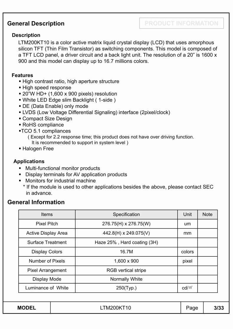
General Description --------------------------------------------------------------------------------- (3)
1. Absolute Maximum Ratings ------------------------------------------------------------------- (4)
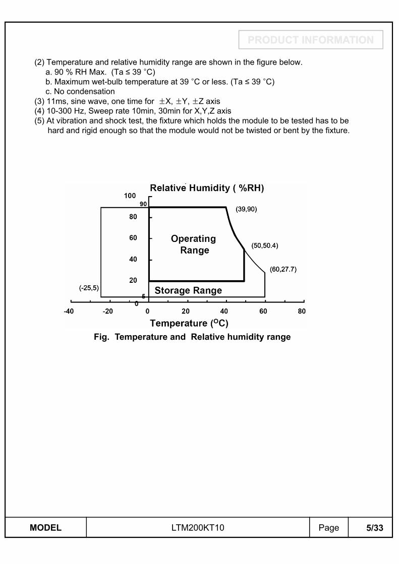
The measurement should be executed in a stable, windless and dark room between
30min after lighting the back light at the given temperature for stabilization
of the back light. This should be measured in the center of screen.
LED forward current : 360 mA Environment condition : Ta = 25 ± 2 °CLED forward current : 360 mA Environment condition : Ta = 25 ± 2 C
Photo detector FieldPhoto detector
Photo detector Field
SR-3 2°
SR-3 : 40㎝RD-80S : 50㎝
Field
LCD Panel
TFT - LCD Module
MODEL LTM200KT10 Page
The center of the screen
7/33
PRODUCT INFORMATIONPRODUCT INFORMATION
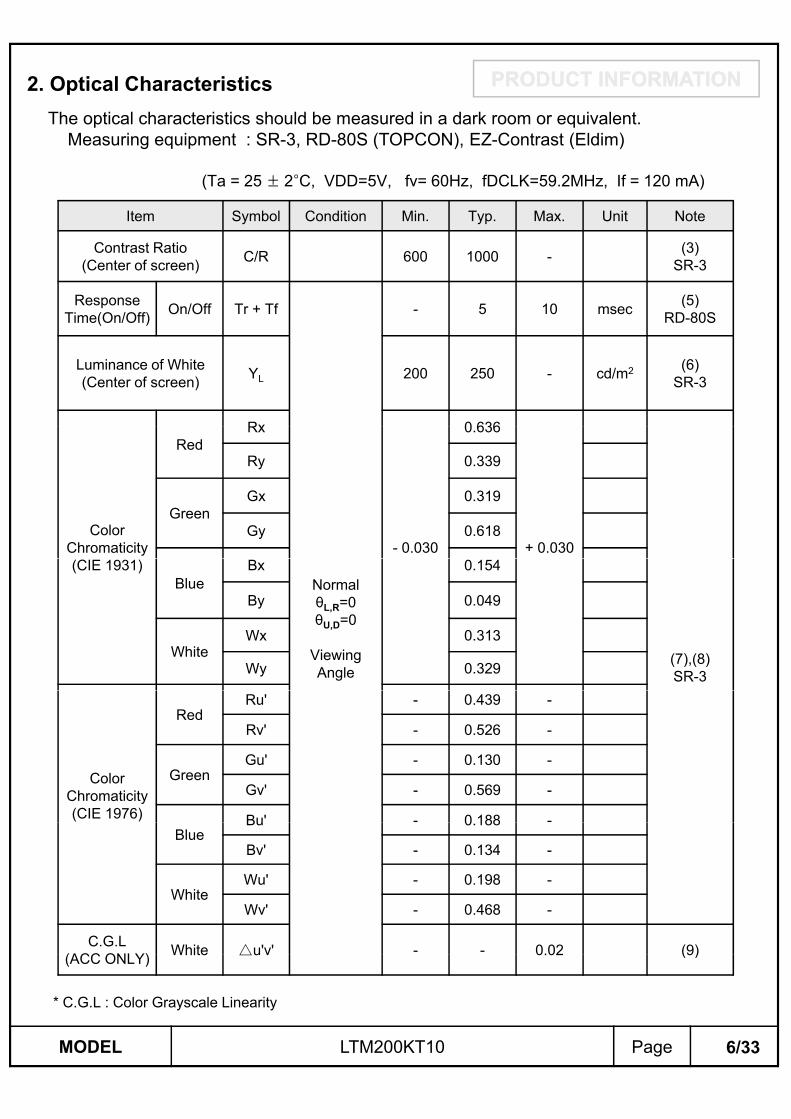
Note (2) Definition of test point
160 800 1440
6
8 79
45
90
450
Active Area
Note (3) Definition of Contrast Ratio (C/R)
: Ratio of gray max (Gmax) & gray min (Gmin) at the center point of the panel
3 2 1 810: Test Point
CRG
G max
min
Gmax : Luminance with all pixels white
Gmin : Luminance with all pixels black
Note (4) Definition of 9 points brightness uniformity
BuniB B
B
100( max min)
max
Bmax : Maximum brightness
Bmin : Minimum brightness
Note (5) Definition of Response time : Sum of Tr, Tf
Display Data White(TFT off) Black(TFT on) White(TFT off)
100%
90%
10%
Optical Instruments
Response
MODEL LTM200KT10 Page
0%
8/33
PRODUCT INFORMATIONPRODUCT INFORMATION
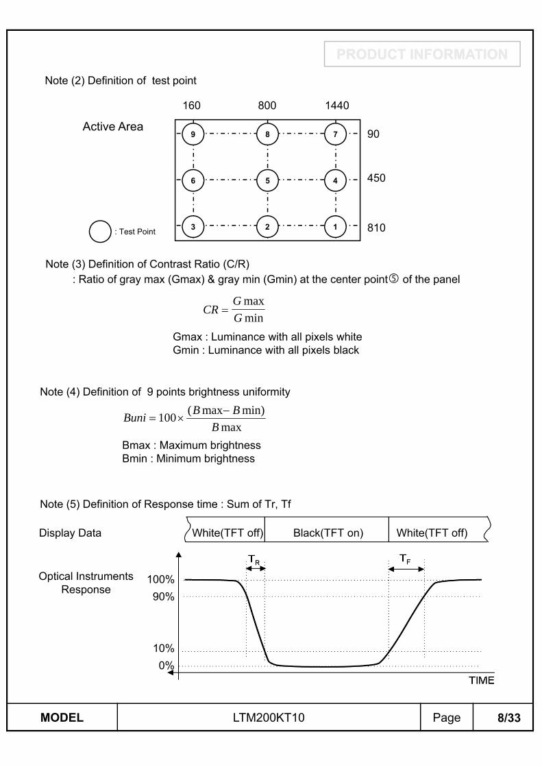
Note (6) Definition of Luminance of White : Luminance of white at center point
Note (7) Definition of Color Chromaticity (CIE 1931, CIE1976)
Color coordinate of Red, Green, Blue & White at center point
Note (8) Definition of Viewing Angle
: Viewing angle range (CR ≥ 10)
MODEL LTM200KT10 Page 9/33
PRODUCT INFORMATIONPRODUCT INFORMATION
Note (9) Color Grayscale Linearity
a. Test image : 100% full white pattern with a test pattern as below
b. Test pattern : Squares, 40mm by 40mm in size, filled with 255, 225, 195, 165, 135 and
105 grays steps should be arranged at the center of the screen.
c. Test method
1st gray step : move a square of 255 gray level should be moved into the center of the-1st gray step : move a square of 255 gray level should be moved into the center of the
screen and measure luminance and u’ and v’ coordinates.
- Next gray step : Move a 225 gray square into the center and measure both
luminance and coordinates, too.
d. Test evaluation
Where A, B : 2 gray levels found to have the largest color differences between them
i.e. get the largest ∆u’ and ∆v’ of each 6 pair of u’ and v’ and calculate the ∆u’v’.
u' v'= (u' - u' ) + (v' - v' )A B2
A B2
MODEL LTM200KT10 Page 10/33
PRODUCT INFORMATIONPRODUCT INFORMATION
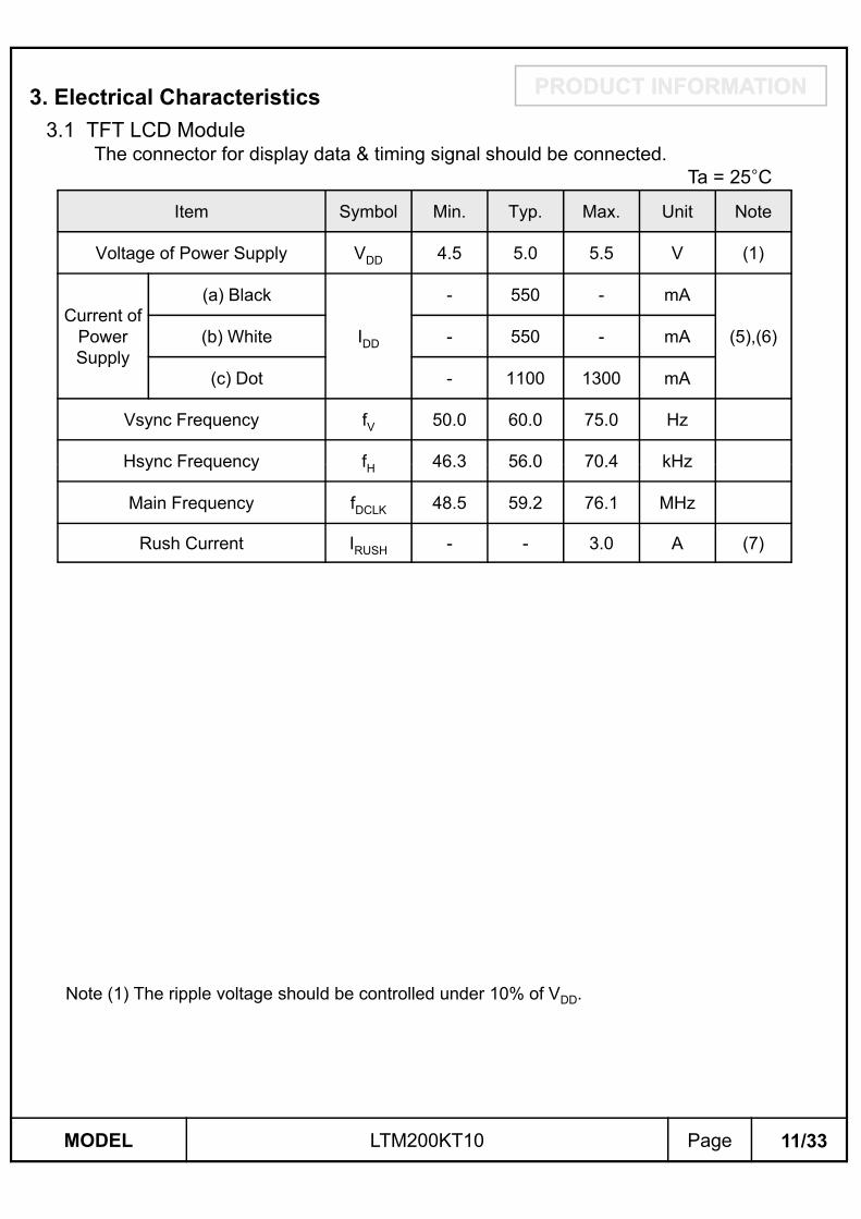
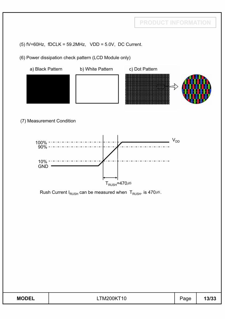
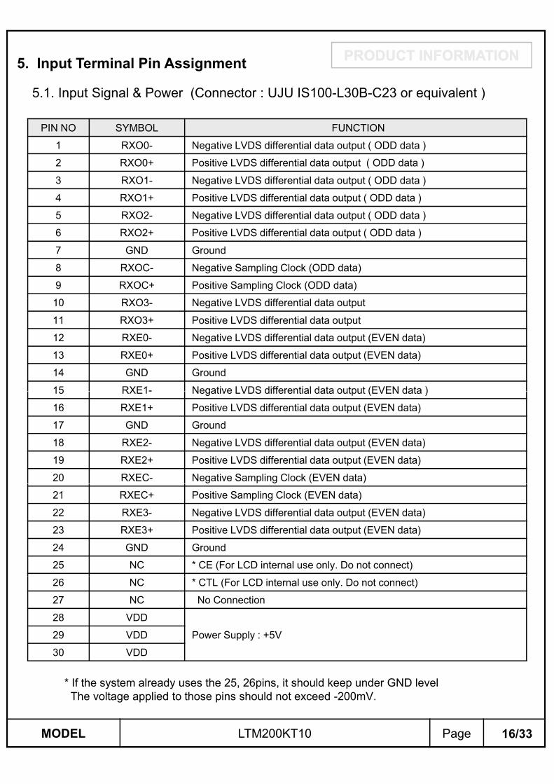
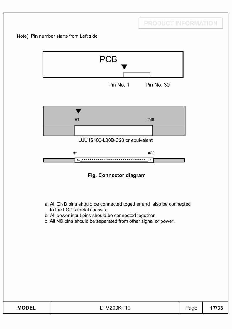
3.1 TFT LCD ModuleThe connector for display data & timing signal should be connected.
Ta = 25°C
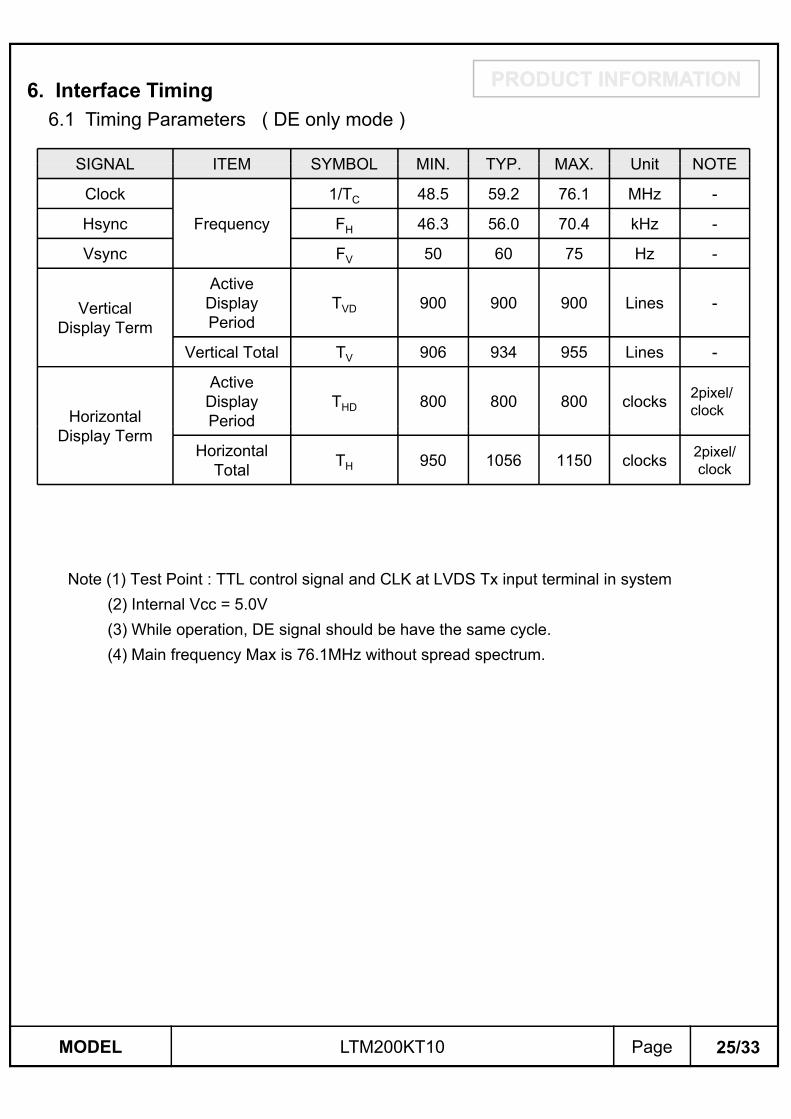
3. Electrical Characteristics
Ta = 25 C
Item Symbol Min. Typ. Max. Unit Note
Voltage of Power Supply VDD 4.5 5.0 5.5 V (1)
Current of
(a) Black - 550 - mA
Current of
Power
Supply
IDD (5),(6)(b) White - 550 - mA
(c) Dot - 1100 1300 mA
Vsync Frequency fV 50.0 60.0 75.0 Hz
Hsync Frequency fH 46 3 56 0 70 4 kHzHsync Frequency fH 46.3 56.0 70.4 kHz
Main Frequency fDCLK 48.5 59.2 76.1 MHz
Rush Current IRUSH - - 3.0 A (7)
Note (1) The ripple voltage should be controlled under 10% of VDD.
MODEL LTM200KT10 Page 11/33
PRODUCT INFORMATIONPRODUCT INFORMATION
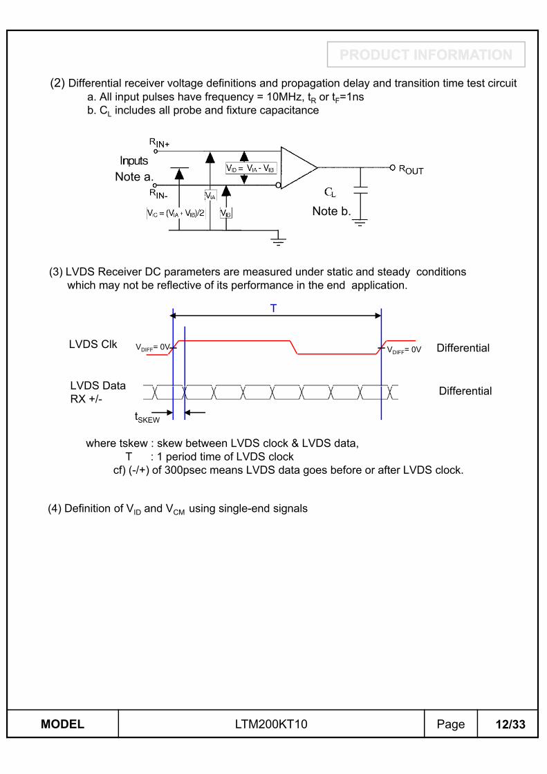
(2) Differential receiver voltage definitions and propagation delay and transition time test circuit
a. All input pulses have frequency = 10MHz, tR or tF=1ns
b. CL includes all probe and fixture capacitanceb. CL includes all probe and fixture capacitance
Note a.
Note b.
(3) LVDS Receiver DC parameters are measured under static and steady conditions
which may not be reflective of its performance in the end application.
Differential
LVDS Data
T
VDIFF= 0V VDIFF= 0VLVDS Clk
where tskew : skew between LVDS clock & LVDS data,
T : 1 period time of LVDS clock
cf) (-/+) of 300psec means LVDS data goes before or after LVDS clock.
LVDS Data
RX +/-
tSKEW
Differential
(4) Definition of VID and VCM using single-end signals
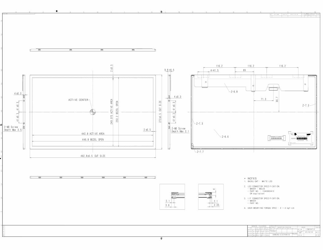
NO PART NAME SPE CI F I CAT I ON Q' TY RE MARKF I N I S H MA T E R I A L
REVISION
35
40
45
50
L M N O P
DESCRI PTI ON OF REVI SI ON REASON CHG' D BY
DE S' D BY
SHEET /
CODE NO. VER.
DRA ' N BY CHK ' D BY APP ' D BYUNI T
SCAL E
TOL E RANCE
mmMODE L NAME
/
SPE C. NO
SAMSUNG E L E CT RONI CS
REV DATE
55
60
65
70
75
Q R S T U V W
PART/ SHEET NAME
ACT I VE CENTER
462. 8±0. 5 OUT SI ZE
272±
0.5
OUT
SIZ
E
442. 8 ACT I VE AREA
446. 8 BEZEL OPEN
2 ±0. 5
249.
075
ACTI
VE A
REA
2±0
.5
9. 8 ±0. 5 4-41. 5
253.
2 BE
ZEL
OPEN
F I L E NO.
L T M2 0 0 KT 1 0
OUTL I NE-DI M. 1 1
0 0
1 . BACKL I GHT : WHI TE L ED
* NOTES
2 . L ED CONNECTOR SPECI F I CAT I ON. - MAKER : MOL EX - PART NO. : 1 0 40 8 6 0 41 0 OR e qu i v a l e n t 3 . I / F CONNECTOR SPECI F I CAT I ON. - MAKER: - PART NO. 4 . USER MOUNTI NG TORQUE SPEC : 3 ~ 4 k g f -c m
2-M3 Sc r ewDept h Max 3 . 5
41±0
.341
±0.3
4 ±0. 3
2-M3 Sc r ewDept h Max 2 . 1
L T M2 0 0 KT XX-XXX
MADE I N C HI NA
XXXXXXXXXXXXXX XXX
71. 3
90.7
69
116. 2 116 . 2 116 . 2
4
2. 1
2 . 3 5
2 . 1
3 . 6
41±0
.341
±0.3
4 ±0. 3
Z-6. 6
Z-7 . 3
Z-7 . 7
Z-9. 8
Z-7 . 3
L J 9 6 -X X X X X X X X X X X X X
X X X X X X X X X X X X X X X X
PRODUCT INFORMATIONPRODUCT INFORMATION
(a) When the module is assembled it should be attached to the system firmly
8. General Precautions
8.1 Handling
(a) When the module is assembled, it should be attached to the system firmly using all mounting holes. Be careful not to twist and bend the module.
(b) Because the inverter uses high voltages, it should be disconnected from power source before it is assembled or disassembled.
(c) Refrain from strong mechanical shock and / or any force to the module.In addition to damage it may cause improper operation or damage to the moduleIn addition to damage, it may cause improper operation or damage to the module and LED back light.
(d) Note that polarizer films are very fragile and could be damaged easily. Do not press or scratch the surface harder than a HB pencil lead.
(e) Wipe off water droplets or oil immediately. If you leave the droplets for a long time staining or discoloration may occurtime, staining or discoloration may occur.
(f) If the surface of the polarizer is dirty, clean it using absorbent cotton or soft cloth.
(g) Desirable cleaners are water, IPA (Isopropyl Alcohol) or Hexane.Do not use Ketone type materials (ex. Acetone), Ethyl alcohol, Toluene, Ethyl acid or Methyl chloride. It might cause permanent damage to the polarizer due to chemicalreactionreaction.
(h) If the liquid crystal material leaks from the panel, it should be kept away from the eyes or mouth . In case of contact with hands, legs or clothes, it must be washed away with soap thoroughly.
(i) Protect the Module from static, or the CMOS Gate Array IC would be damaged.
(j) Use finger-stalls with soft gloves in order to keep display clean during the incoming inspection and assembly process.
(k) Do not disassemble the Module.
(I) Do not adjust the variable resistor located on the Module.
(m) Protection film for polarizer on the Module should be slowly peeled off just before useso that the electrostatic charge can be minimized.
(n) Pins of I/F connector should not be touched directly with bare hands.
MODEL LTM200KT10 Page 31/33
PRODUCT INFORMATIONPRODUCT INFORMATION8.2 Storage
(a) Do not leave the Module in high temperature, and high humidity for a long time.
It is highly recommended to store the Module with temperature from 5 to 40℃It is highly recommended to store the Module with temperature from 5 to 40℃and relative humidity of less than 70%.
(b) Do not store the TFT-LCD Module in direct sunlight.
(c) The Module should be stored in a dark place. It is prohibited to apply sunlight or
fluorescent light in storingfluorescent light in storing.
(d) Storage period is recommended not to exceed 1 year.
8.3 Operation
(a) Do not connect or disconnect the Module in the "Power On" condition.
(b) Power supply should always be turned on/off by the item 6.3
"Power on/off sequence"
(c) Module has high frequency circuits. Sufficient suppression to the electromagnetic
interference should be done by system manufacturers. Grounding and shielding
methods may be important to minimize the interference.
8.4 Operation Condition Guide
( ) Th LCD d h ld b d d l di i(a) The LCD product should be operated under normal conditions.
(b) If the product will be used in extreme conditions such as high temperature(b) If the product will be used in extreme conditions such as high temperature,
humidity, display patterns or operation time etc.., It is strongly recommended
to contact SEC for Application engineering advice. Otherwise, its reliability and
function may not be guaranteed. Extreme conditions are commonly found at
Airports, Transit Stations, Banks, Stock market, and Controlling systems.
MODEL LTM200KT10 Page 32/33
PRODUCT INFORMATIONPRODUCT INFORMATION
8.5 Others
( ) Ul i l fil i f d i(a) Ultra-violet ray filter is necessary for outdoor operation.
(b) Avoid condensation of water. It may result in improper operation or disconnection
of electrode.
(c) Do not exceed the absolute maximum rating value. ( supply voltage variation,
input voltage variation variation in part contents and environmental temperatureinput voltage variation, variation in part contents and environmental temperature,
and so on)
Otherwise the Module may be damaged.
(d) If the Module keeps displaying the same pattern for a long period of time,
the image may be “stuck" to the screen.
To avoid image sticking it is recommended to use a screen saverTo avoid image sticking, it is recommended to use a screen saver.
(e) This Module has its circuitry PCB's on the rear side and should be handled
carefully in order not to be stressed.
(f) Please contact SEC in advance when you display the same pattern for a long time.


![SAMSUNG TFT-LCD MODEL A460HN08W(HD,60HZ) · LTY[Z]460HN05 is a color active matrix liquid crystal display (LCD) that uses amorphous silicon TFT(Thin Film Transistor) as switching](https://static.documents.pub/doc/80x56/5e813674375a7e757f1cdfd4/samsung-tft-lcd-model-a460hn08whd60hz-ltyz460hn05-is-a-color-active-matrix.jpg)