IBIS OPEN FORUM I/O BUFFER MODELING COOKBOOK Version 4.0 Revision 0.4 Prepared By: The IBIS Open Forum Senior Editor: Michael Mirmak Intel Corp. From an original by Stephen Peters Rev 0.0 - August 10, 2004 Rev 0.1 – September 9, 2004 Rev 0.2 – October 5, 2004 Rev. 0.4 – October 15, 2004 – added series/series switch descriptions; incorporated written feedback from Arpad, updated the single-ended totem-pole buffer diagrams, reformatted document with appropriate labels and table of contents; used buffer or component in place of device in many cases;
Transcript
IBIS OPEN FORUMI/O BUFFER MODELING COOKBOOK
Version 4.0
Revision 0.4
Prepared By:
The IBIS Open Forum
Senior Editor:
Michael MirmakIntel Corp.
From an original by Stephen Peters
Rev 0.0 - August 10, 2004
Rev 0.1 – September 9, 2004
Rev 0.2 – October 5, 2004
Rev. 0.4 – October 15, 2004 – added series/series switch descriptions; incorporated written feedback from Arpad, updated the single-ended totem-pole buffer diagrams, reformatted document with appropriate labels and table of contents; used buffer or component in place of device in many cases; incorporated new SSO language; added new differential type diagrams.
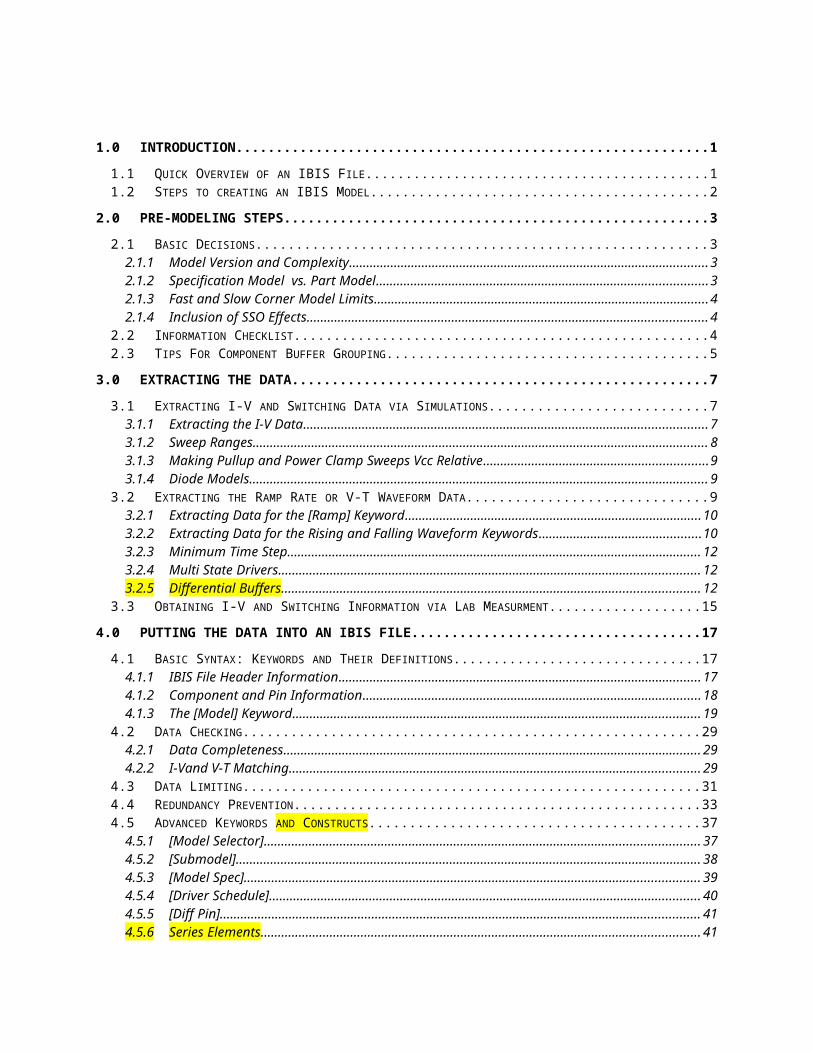
1.1 QUICK OVERVIEW OF AN IBIS FILE........................................................................................................ 11.2 STEPS TO CREATING AN IBIS MODEL......................................................................................................2
2.1 BASIC DECISIONS................................................................................................................................... 32.1.1 Model Version and Complexity......................................................................................................... 32.1.2 Specification Model vs. Part Model..................................................................................................32.1.3 Fast and Slow Corner Model Limits..................................................................................................42.1.4 Inclusion of SSO Effects.................................................................................................................... 4
2.2 INFORMATION CHECKLIST...................................................................................................................... 42.3 TIPS FOR COMPONENT BUFFER GROUPING..............................................................................................5
3.0 EXTRACTING THE DATA................................................................................................................... 7
3.1 EXTRACTING I-V AND SWITCHING DATA VIA SIMULATIONS....................................................................73.1.1 Extracting the I-V Data..................................................................................................................... 73.1.2 Sweep Ranges................................................................................................................................... 83.1.3 Making Pullup and Power Clamp Sweeps Vcc Relative.....................................................................93.1.4 Diode Models.................................................................................................................................... 9
3.2 EXTRACTING THE RAMP RATE OR V-T WAVEFORM DATA......................................................................93.2.1 Extracting Data for the [Ramp] Keyword........................................................................................103.2.2 Extracting Data for the Rising and Falling Waveform Keywords.....................................................103.2.3 Minimum Time Step......................................................................................................................... 123.2.4 Multi State Drivers.......................................................................................................................... 123.2.5 Differential Buffers......................................................................................................................... 12
3.3 OBTAINING I-V AND SWITCHING INFORMATION VIA LAB MEASURMENT................................................15
4.0 PUTTING THE DATA INTO AN IBIS FILE......................................................................................17
4.1 BASIC SYNTAX: KEYWORDS AND THEIR DEFINITIONS...........................................................................174.1.1 IBIS File Header Information..........................................................................................................174.1.2 Component and Pin Information......................................................................................................184.1.3 The [Model] Keyword..................................................................................................................... 19
4.2 DATA CHECKING.................................................................................................................................. 294.2.1 Data Completeness.......................................................................................................................... 294.2.2 I-Vand V-T Matching...................................................................................................................... 29
4.3 DATA LIMITING.................................................................................................................................... 314.4 REDUNDANCY PREVENTION.................................................................................................................. 334.5 ADVANCED KEYWORDS AND CONSTRUCTS...........................................................................................37
1.0 IntroductionThis cookbook describes the steps required to produce IBIS models for digital integrated circuits (ICs). IBIS (officially, EIA standard 656-A, IEC 62014-1) stands for I/O Buffer Information Specification. IBIS models provide a standardized way of representing the electrical characteristics of an digital IC’s pins (input, output, or I/O buffers) behaviorally, i.e., without revealing the underlying circuit’s structure or process information.
The purpose of this document is to explain describe how to gather the information required to produce an IBIS model, as well as some of the common pitfalls to avoid when creating the IBIS file itself. Note that the basic behavioral information in an IBIS model can be obtained either by direct measurement of the component device itself or transistor level simulation of the device’s component’s circuits buffers. This cookbook describes both methods. The cookbook is targeted towards generating models of CMOS, GTL, and bipolar parts, and applies to models generated for IBIS versions 3.2 and 4.0. For the most recent version of the specification and other IBIS documents visit the IBIS web page. For access information, see the Resources section later in this cookbook.
The intended audience of this cookbook is are those responsible for performing the measurements or simulations that gather I/O buffer data, as well as those responsible for actual IBIS model creation. Persons involved in SI or system level PC board simulations may also benefit by reading this document. It is assumed that the reader has some familiarity with behavioral modeling of I/O buffers and analog simulation.
1.1 Quick Overview of an IBIS File
An IBIS file contains, in a human readable ASCII format, the data required to behaviorally model a device’s component’s input, output and I/O buffers. Specifically, the data in an IBIS file is used to construct a model useful for performing signal integrity (SI) simulations and timing analysis of printed circuit (PC) boards. The fundamental information needed to perform these simulations is a buffer’s I-V (current vs. voltage) and switching (output voltage vs. time) characteristics. Please note that the IBIS specification does NOT define an executable simulation model – it is a standard for the formatting and transfer of data. As such, the specification defines what the information included in an IBIS file represents and how it is to be gathered. It does not specify what an analog simulation application does with the data.
IBIS models are component-centric. That is, an IBIS file allows one to model an entire component, not just a particular input, output or I/O buffer. Therefore, in addition to the electrical characteristics of a device component’s buffers an IBIS file includes a device component’s pin-to-buffer mapping, and the electrical parameters of the device component’s package.
In general an output or I/O pin (buffer) is characterized behaviorally using the following information:
The buffer’s output I-V characteristics when the output is in the logic low state The buffer’s output I-V characteristics when the output is in the logic high state The buffer’s output I-V characteristics when the output is forced below ground and above the
power supply rail (referred to as its ‘beyond the rail’ characteristics) The time it takes a buffer’s output to switch logic states (i.e. from low to high and high to low) The buffer’s capacitance
For an input buffer the required information is reduced to:
IBIS Forum I/O Buffer Modeling Cookbook Page 1
The buffer’s input I-V characteristics (including its ‘beyond the rail’ characteristics) The buffer’s capacitance
The above information is included in an IBIS file using ‘keywords’. A keyword is a word or phrase surrounded by square brackets. Keywords are followed either by specific parameters or tables of data. As an example For instance, the keyword used to introduce the data that makes up a specific buffer’s model is [Model] the [Model] keyword would be used to encapsulate the I-V and V-T tables, plus other data, for individual single-ended I/O buffer. Some keywords are required, but most are optional. At a minimum, a valid IBIS file contains the following data and keywords.
1. Information regarding the file itself and name of the component being modeled. This information is contained under the keywords [IBIS Ver], [File Name], [File Rev], [Component] and [Manufacturer].
2. Information about the package’s electrical characteristics and the pin to buffer model mapping (i.e. which pins are connected to which buffer models). This information is included under the [Package] and [Pin] keywords.
3. The data required to model each unique input, output and I/O buffer design on the device component. The [Model] keyword introduces the data set for each unique buffer. As describe above, buffer are characterized by their I-V tables and switching characteristics. This information is included using the keywords [Pullup], [Pullown], [GND clamp], [POWER Clamp] and [Ramp]. In addition, the required parameters to the [Model] keyword specify a models type (input, output, I/O, open_drain, etc.) and its input or output capacitance.
The details of constructing an IBIS model from data are included in the chapter Putting the Data Into an IBIS File later in this document.
1.2 Steps to creating an IBIS Model
There are five basic steps to creating an IBIS model of a component:
1. Perform the pre-modeling activities. These include deciding on the model’s complexity, determining the voltage, temperature and process limits over which the IC operates and the buffer model will be characterized, and obtaining the component device-related (electrical characteristics and pin-out) and use information about the component. See the chapter titled Pre-Modeling Steps.
2. Obtain the electrical (I-V tables and rise/fall) data for output or I/O buffers either by direct measurement or by simulation. See the chapter titled Extracting the Data. This chapter is can may also be used by those who are doing the simulations required to gather the data but not actually creating the IBIS file.
3. Format the data into an IBIS file and run the file through the Golden Parser. See the chapter titled Putting Data Into an IBIS File.
4. If the model is generated from simulation data, validate the model by comparing the results from the original analog (transistor level) model against the results of a behavioral simulator that uses the IBIS file as input. See the chapter titled Validating the Model.
5. When the actual silicon is available (or if the model is from measured data), compare the IBIS model output to the measured output. See the chapter titled Correlating the Data.
The rest of this cookbook documents these steps in detail.
Page 2 I/O Buffer Modeling Cookbook IBIS Forum
2.0 Pre-Modeling Steps2.1 Basic DecisionsBefore one creates an I/O buffer model there are several basic questions that must be answered regarding the model’s complexity, operational limits, and use requirements. Answering these questions requires not only a knowledge of the buffer’s physical construction, but also a knowledge of the final application in which the IC will be used, and any specific requirement the model users may place on the model. These questions cannot be answered by the model creator alone; they generally require the involvement of both the buffer designer and members of the team responsible for insuring that the I/O buffers are useable in a system environment. This team is referred to as the interconnect simulation team. Together, the model creator and interconnect simulation team must determine the following:
2.1.1 Model Version and Complexity Based on the characteristics and construction of the I/O buffer itself, and the model user’s simulator capability, you must decide what IBIS version of the model to make. Following good engineering practice use the simplest model that will suffice. For standard CMOS buffers with a single stage push-pull or open drain outputs a version 1.1 model is the starting point. A version 1.1 models allows a buffer to be described using a low state and high state I-V table, along with a linear ramp that describes how fast the buffer switches between states. IBIS version 2.1 adds support for ECL and dual-supply buffers, ground bounce from shared power rails, differential I/O devices buffers, termination components, and controlled rise-time buffers. A version 2.1 or above model will be required if the I/O buffer has any of the following characteristics:
Multiple Supply Rails -- A version 2.1 model is require if the EDS ESD diodes are connected to a different power rail than the pullup or pulldown transistors, or if the I/O uses more than one supply (for example, a buffer whose output swings from below ground or above Vcc).
Non-Linear Output Switching Waveform – A version 2.1 (or higher) model is required if the I/O buffer’s output voltage vs. time waveform (its V-T waveform) when switching low-to-high or high-to-low is significantly non-linear. This is the case for GTL technology, or for any device buffer that uses “graduated turn on” type technology. Note that even if an I/O buffer can be modeled successfully using IBIS version 1.1, a version 2.1 model must be used if the project wants to take advantage of the V-T waveform tables in version 2.1 in order to give the user a “golden waveform”.
In addition, a version 2.1 model description is required if the model maker wishes to enable the user to perform ground bounce simulations via ganging several buffers together on a common supply rail.
As currently planned, IBIS version 3.2 and above adds supports for an electrical board description, multi-staged or multi-I-V devices buffers and diode transient times, among other features.
2.1.2 Specification Model vs. Part Model A model can be made to represent a specific existing component or can be made as a representative (non-existing) encapsulation of an external specification. Specification vs. Part is a major factor in determining if and how much guard-banding or de-rating a model requires. Generally, a “spec model” is based on an existing part, then the strength and edge rate of the model is adjusted to meet the best and worst case parameters of a particular specification. For example, an GTL buffer model for a particular processor may give a worst case Vol of 0.4 V at 36 mA. However, if the GTL specification allows for a worst case Vol of 0.6 V at 36 mA the model’s pulldown table may be adjusted (or de-rated) to just meet this describe the specification and not just the behavior of an individual part. In this way the same IBIS model can be used to represent a whole series of devices, and not just one particular device.
IBIS Forum I/O Buffer Modeling Cookbook Page 3
2.1.3 Fast and Slow Corner Model LimitsThe IBIS format provides for slow (weakest drive, slowest edge), typical and fast (strongest drive, fastest edge) corner models. These corners are generally determined by the environmental (temperature and power supply) conditions under which the silicon is expected to operate, the silicon process limits, and the number of simultaneous switching outputs. The interconnect team or project must supply the model developer with the environmental, silicon process, and operational (number of SSOs) conditions that define the slow, typical and fast corners of the model. Please note that for an output buffer model to be useful for flight time simulations these conditions MUST match those used for specifying the buffer’s Tco parameter.
2.1.4 Inclusion of SSO EffectsClosely related to the discussion on model limits is the decision on how to include Simultaneous Switching Output (SSO) effects. SSO effects can be included explicitly in a model by measuring the I-V and edge rate characteristics under SSO conditions. For example, a buffer’s I-V characteristic can be measured with all the adjacent buffers turned on and sinking current, or the buffer’s edge rate may be measured while adjacent buffers are also switching. Alternatively, a model that represents a single buffer in isolation may be created, then several buffers may be connected to a common power or ground rail via the [Pin Mapping] keyword. The former method (including SSO effects in the models’ I-V and edge rate tables) has the advantage that the resulting model is straight forward to verify and less dependent on any particular simulator’s capability. Note however, the [Pin Mapping] keyword method does give the user the ability to perform explicit ground bounce simulations and devise specific ‘what if’ scenarios.Note that the information provided under IBIS 4.0 and earlier versions only describes the output behavior of buffers under loaded conditions. Therefore, SSO simulations will only be based on the behavior at the pad and not upon information extracted about the current profile of the supplies as the buffer switches. Different distributions of internal buffer current may result in the same behavior at the pad. Different simulation tools may therefore make radically different assumptions regarding SSO behavior for the same IBIS data. Check with your simulation tool vendor for details on their specific assumptions and IBIS SSO simulation algorithms.
2.2 Information ChecklistOnce the above decisions have been made, the model maker can begin the process of acquiring the specific information needed to generate an the IBIS model of a for the component. Some of this information is specific to the component as a whole and goes directly into the IBIS file itself, while some items are needed to perform the required simulations. In general, the model maker will need the following:
IBIS Specification Acquire, read and become familiar with the IBIS specification.
Buffer Schematics Acquire a schematic of each of the different types of input, output and I/O buffers on the component. If at all possible, use the same schematic that the silicon designers use for simulating Tco. Make sure that the schematic includes ESD diodes (if present in the design) and a representation of the power distribution network of the package. From these schematics determine the type of output structure (standard CMOS totem-pole, open-drain, etc.) for each different type of output or I/O buffer on the IC.
Clamp Diode and Pullup references Determine if the device buffer uses a different voltage reference (power supply rail) for the clamp diodes than that used for the
Page 4 I/O Buffer Modeling Cookbook IBIS Forum
pullup or pulldown transistors. This may be the case when dealing with components that are designed to be used in mixed 3.3 V/5 V systems.
Packaging information Find out in what packages the device component is offered. A separate IBIS model is required for each package type. Acquire a pinout list of the device component (pin name to signal name mapping) and determine the pin name to buffer type mapping.
Packaging Electricals Acquire a copy of the devices package model – specifically the electrical characteristics (inductance, capacitance and resistance) of the component’s package for each pin to buffer connection (package stub). This information becomes the R_pin, L_pin and C_pin parameters of the [Pin] keyword or the R_pkg, L_pkg and C_pkg of the [Package] keyword.
Signal information Determine which signals can be ignored for modeling purposes. For example, test pads or static control signals may not need an I/O a model. These may be listed as NC in the [Pin] list.
Die capacitance Get Obtain the input, output, or I/O capacitance of each pad (the C_comp parameter). This is the capacitance seen when looking from the pad back into the buffer for a fully placed and routed buffer design, exclusive of package effects (note that Cdie or die capacitance may be used in other industry contexts to refer to the capacitance of the entire device component as measured between rails).
Vinl and Vinh Parameters A complete IBIS model of an input or I/O buffer includes the Vinl and Vinh parameters. Vinl is the maximum pad or pin voltage at which the receiving buffer’s logical state would still be a logical “low” or “0.” Vinh is the minimum pad or pin voltage at which the receiving buffer’s logical state would still be a logical “high” or “1.”
Tco Measurement Conditions Find out under what loading conditions an output or I/O buffer’s Tco (propagation delay, clock to output) parameter is measured. This includes the load capacitance, resistance and voltage (Cref, Rref and Vref parameters) as well as the output voltage crossing point at which Tco is measured (the Vmeas parameter).
2.3 Tips For Component Buffer GroupingOne of the first tasks when building an IBIS model of a component is determining how many individual buffer models have to be created. Separate buffer models are required for each different buffer design or structure (number and connection of the transistor elements) the component uses. Begin by first separating a component’s pins into inputs, outputs and I/Os. Then for each group of pins determine how many buffer designs are present. For example, a clock input may have a different input design or diode structure than the rest of the component’s’ inputs. Also, be aware that even if all the output or I/O signals are driven by the same buffer design, separate output or I/O models may be required if a group of
IBIS Forum I/O Buffer Modeling Cookbook Page 5
signals have different C_comp parameters or Tco measurement conditions. Once the number of separate buffer models has been determined, the actual buffer model creation process can begin.
Page 6 I/O Buffer Modeling Cookbook IBIS Forum
3.0 Extracting the DataOnce the pre-modeling steps have been performed, the process of gathering the components required I-V and switching information can begin. Output and I/O buffers need both I-V tables and rise/fall times, input buffer require I-V tables only. There are two ways to get this information:
• For pre-silicon models use circuit simulation tools to obtain the information over the worst cases of process and temperature variations, then correlate the model against the actual silicon.
• When the actual silicon is available, use the data from physical measurements to build the model. However, it is difficult to get worst case min and max data over process and temperature this way.
The first sections of this chapter explains how to obtain the I-V and V-T information from a transistor level model of the buffer, either by use of the Spice to IBIS translator or by doing your own simulations. Section 3.3 in this chapter explains how to gather this information via measurement. It is assumed that the reader has some background in doing transistor level simulations and/or the use of lab equipment.
3.1 Extracting I-V and Switching Data via SimulationsA model creator can extract the required I-V and V-T information directly through their own simulations. The following section explains how to perform these simulations.
3.1.1 Extracting the I-V DataThe first step to extracting the required I-V tables is understanding the buffer’s operation. Analyze the buffer schematic and determine how to put the buffer’s output into a logic low, logic high and (if applicable) high impedance (3-state) state. As mentioned above, the schematic should include the R, L and C parameters associated with the on die power supply distribution and ground return paths as well as any ESD or protection diodes. The schematic should also indicate if the power clamp or ground clamp diode structures are tied to a voltage rail (voltage reference) different than that used by the pullup or pulldown transistors.
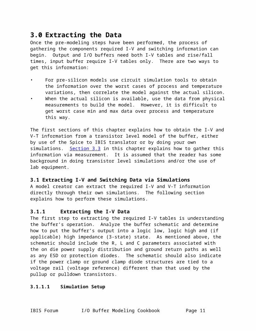
3.1.1.1 Simulation SetupA typical simulation setup for an output or I/O buffer is shown in Figure 1 below. For this example the device under test (DUT) the buffer being analyzed is a standard 3-state buffer with a single push-pull output stage.
Figure 1 - Example I-V Simulation Setup
All measurement are made at the output node (pad) as shown above. Remove all package lead (R_pin, L_pin, C_pin) parasitics. However, any series resistors present between the pad and the pullup/pulldown transistors are included.
The output buffer is connected to an independent voltage source. Set the buffer’s input(s) so that the desired output state (low, high, off) is obtained, then using a DC or ‘transfer function’ analysis sweep the voltage source over the sweep range -Vcc to Vcc * 2 while recording the current at the output node. If a DC analysis causes convergence problems an alternative method is to do a ‘transient analysis’. The voltage source becomes a slow (100 mV/ms) linear ramp function driving the output node. The current into the output node is measured, as is the voltage at the node with respect to a lab reference, then the resulting I-T and V-T data is combined into a single I-V table. Note that a transient function analysis may require post simulation data manipulation.3.1.1.2 3-state Buffers
IBIS Forum I/O Buffer Modeling Cookbook Page 7
For an I/O (3-stateable) buffer, four sets of I-V tables are required; one with the pulldown transistor turned on (output in the low state), one with the pullup transistor turned on (output in the high state), and two with the output in a high impedance state. The data gathered while the output is in the low state is used to construct the [Pulldown] table. Data gathered when the output is in the high state is used to construct the [Pullup] table. Pulldown I-V data is referenced to ground while pullup I-V data is referenced to Vcc. (Referencing pullup data to Vcc means that the endpoints of the sweep range are adjusted as Vcc is adjusted; refer to the section titled Making Pullup and Power Clamp Sweeps Vcc Relative for more details.) Data for the [GND Clamp] keyword is taken with the output in the high impedence state and is ground relative, while data for the [POWER Clamp] keyword is also taken with the output in a high impedance state but with the data Vcc relative. Each set of tables must be repeated under the minimum, typical and maximum corner conditions and must cover the entire sweep range.
Thus, a buffer with 3-state capabilities would require the following 12 I-V data sets:
Pulldown I-V under minimum, typical and maximum conditions, data ground relative Pullup I-V under minimum, typical and maximum conditions, data Vcc relative High Impedance state I-V under minimum, typical and maximum conditions, data ground
relative High Impedance state I-V under minimum, typical and maximum conditions, data Vcc relative
3.1.1.3 Output Only BuffersFor a output only (non 3-state) output buffer only two sets of tables are needed; one with the pulldown transistor turned on (output in the low state), and one with the pullup transistor turned on (output in the high state). As before, pulldown I-V data is referenced to ground while pullup I-V data is referenced to Vcc. Because an output only buffer does not have a 3-state mode the power and ground clamp diode tables cannot be isolated from the transistor tables; the beyond the rail data is simply included in the pullup and pulldown I-V data. The [GND Clamp] and [POWER Clamp] keywords are not required for an output only buffer.
3.1.1.4 Open Drain BuffersOpen-drain or open-collector type devices buffers only require three sets of I-V data: [Pulldown], [GND Clamp] and [POWER Clamp]. Data for the [Pulldown] table is gathered as described previously. [POWER Clamp] and [GND Clamp] data is gathered by turning off the pulldown transistor then doing the two I-V sweeps as described above for an I/O buffer in the high impedance state. Note that an open drain buffer may not require the full -Vcc to Vcc * 2 sweep range; refer to the section below entitled Sweep Ranges.
3.1.1.5 Input BuffersWhen gathering I-V data for input buffers the same general setup is used, only the variable voltage source is placed on the input node. Input buffers require only [POWER Clamp] and [GND Clamp] I-V data. As with the output buffer, [GND Clamp] data is gathered via a voltage sweep with the voltage source referenced to ground and the [POWER Clamp] data is gathered by a voltage sweep with the voltage source Vcc relative. If an input device buffer includes weak resistors to power or ground their I-V tables are included into the respective ground clamp or power clamp I-V data.
3.1.2 Sweep Ranges As per the IBIS specification I-V data must be supplied over the range of voltages the output could possible see in a transmission line environment. Assuming that a devices’ buffer’s output swings from ground to Vcc (where Vcc is the voltage given by the [Voltage Range] or [Pullup Reference] keywords) this range is -Vcc (the maximum negative reflection from a shorted transmission line) to Vcc *2 (the
Page 8 I/O Buffer Modeling Cookbook IBIS Forum
maximum positive reflection from an open circuited transmission line). However, be aware that if a device buffer is operating in an environment where its output could be actively driven beyond these limits the I-V table must be extended further. Consider, for example, a 3.3 V I/O buffer operating in a mixed 3.3 V/5 V system. While the device buffer’s output may only drive from 0 to 3.3 V, a five volt device buffer connected to this output may drive the output node beyond 3.3 V volts. In this case I-V data should be supplied over a full -5 V to +10 V range. Likewise, an open collector or open drain device buffer may be terminated in a voltage (Vpulllup) different than that given by the [Voltage Range] keyword. In this case it is permissible to supply the pullup and pulldown data over the range -Vpullup to Vpullup *2.
It is recognized that semi-conductor device buffer models may not be well behaved over these ranges, so it is acceptable to lessen the actual sweep range then use linear extrapolation to get to the required endpoints. For example, suppose one were attempting to gather the I-V data for a typical 5 V device buffer. The IBIS specification requires I-V data over the full -5 V to 10 V range. The model maker may choose to limit the simulation sweep to -2 V to +7 V, and then extrapolate to the final -5 V to +10 V range. Be aware however, that the simulation sweep range must be enough to forward bias any ESD/protection diodes or the diodes intrinsic to the output transistor structures.
3.1.3 Making Pullup and Power Clamp Sweeps Vcc Relative As stated earlier the pullup and power clamp data is relative to Vcc. In order to make the pullup and power clamp data Vcc relative (and to enter this I-V data into IBIS’s table format properly) adjust the starting and ending endpoints of these sweep to follow the variations in Vcc. For example, suppose one where gathering the pullup data for a standard 3.3 V device buffer whose Vcc specification was 3.3 V +/- 10% (i.e. the operating Vcc ranged from 3.0 V minimum to 3.6 V maximum). The sweep voltage under typical conditions would range from -3.3 V to +6.6 V. For minimum conditions, where the Vcc was adjusted to 3.0 V, the sweep voltage should also be adjusted negative 0.3 V, to sweep from -3.6 V to +6.3 V. Likewise, for maximum conditions, adjust the sweep endpoint positive 0.3 V so the sweep covers -3.0 V to 6.9 V. By gathering the data in this manner the corresponding voltage data point in all three data sets represent the same ‘distance’ from Vcc. Note that the 9.9 V sweep RANGE remains the same for all three simulations.
3.1.4 Diode ModelsWhen doing digital I/O buffer designs most of the analysis is concerned with the buffer’s Tco parameter and output impedance. Very little attention is paid to a buffer’s ‘beyond the rail’ operation. Thus, the diode models included in buffer’s schematic may be included for layout or completeness only, and are most likely ‘perfect’ diodes with no intrinsic resistance. Likewise, if the design relies on the intrinsic diode structure of the output transistors to provide output protection the transistor models may not properly model this mode of operation. Therefore, when doing simulation in these voltage regions one may get unrealistically large (e.g., kiloamp) power and ground clamp currents. If this is a problem the model creator has a couple of options. Working with the buffer designer the diode or transistor models can be enhanced to include the proper junction or bulk resistance. Note that with large ESD structures the metal resistance can be relatively large—on the order of a few ohms – an this should be included in the design. If an actual device buffer is available the model creator can measure the power and ground clamp I-V data directly.
3.2 Extracting the Ramp Rate or V-T Waveform DataSimulations to obtain the ramp rate and/or V-T (output voltage vs. time) tables are relatively straight forward. For each simulation corner (minimum, typical, maximum) four two V-T data sets are required; one rising and one falling set for the buffer output switching low to high, the other is and one rising and
IBIS Forum I/O Buffer Modeling Cookbook Page 9
one falling set for the buffer output switching high to low. This data can then be reported as a rising and falling dV/dt ratios (the ‘ramp rate’) or the actual V-T data may be reported directly.
3.2.1 Extracting Data for the [Ramp] KeywordIf the output switching (V-T) waveform of a device buffer can be approximated by a linear ramp (i.e. the V-T waveform has no abrupt changes in shape, there are no ‘pedestals’ in the waveform, etc.) then the V-T data may be reported as a rising and falling ramp rate (dV/dt) by using the [Ramp] keyword. Data for the [Ramp] keyword is extracted using the simulation setup shown in figure two below. This setup is the one described in IBIS versions 1.1 and 2.1, and is applicable for extracting rise and fall data for a standard single stage, push-pull TTL or CMOS buffer.
Figure 2 – Simulation Setup for extracting Ramp Rate Information
Obtain rise and fall time data by setting the simulator for a transient analysis simulation. The control inputs of the buffer are set to enable the buffer outputs and a driving waveform is applied to the buffer input. The slew rate of the input stimulus driving waveform should match the internal slew rate of the technology (i.e. the slew rate of the pre-driver that would normally drive the final output stage). Rising edge ramp rate data is obtained by placing a load resistance from the output to ground then stimulating the buffer so that the output switches from low to high. Falling edge ramp data is captured with the load resistor tied to Vcc. Use a load resistance of 50 ohms. If the device buffer does not have enough drive capability to make a significant output transition then a higher value of load resistance may be used, but this must be noted in the IBIS file (see the description of the [Ramp] keyword in the IBIS specification for specific details). For an open drain or ECL type device buffer s, measure the rise and fall times into the load resistor and voltage used by the manufacture when specifying propagation delays. As with the I-V simulations the package lead (L_pin, R_pin, C_pin) parasitics must be removed. However, simulations are performed with C_comp included in the circuit. Note that to avoid errors when trying to correlate later simulations with those used to extract rise/fall time information, use the same “time step” throughout the simulation and correlation procedure.
3.2.2 Extracting Data for the Rising and Falling Waveform KeywordsIn IBIS version 2.1 V-T data may be reported directly by using the [Rising Waveform] and [Falling Waveform] keywords. These two keywords are generally required if the output switching waveform of the device buffer is significantly non-linear (this is the case with most ‘controlled rise time’ or ‘graduated turn on’ style buffers). The use of these keywords is also indicated if the device buffer incorporates a delay between the turning off of one output transistor and the turning on of the other (i.e. the V-T waveform contains a pedestal). Finally, the model creator may wish to include the V-T data directly so that the model itself includes it own verification feature. By including this ‘golden waveform’ the model user may perform a simulation with the buffer driving the same load as was used to generate the V-T waveforms. The results of this simulation should match the V-T waveform as given in the IBIS file, thereby verifying that the users simulator is producing the proper results.
When doing simulations to extract V-T data for the [Rising Waveform] and [Falling Waveform] keywords a variety of load circuits are used, depending on the technology of the buffer. The intent is that by picking the proper load(s) and termination voltage(s), the turn-on time, turn-off time (and overlap between the two) of the pullup and pulldown stages of the buffer can be isolated and a more accurate behavioral model constructed. Following are the recommended loads and waveforms to collect, as specified by the various CAE vendors that support IBIS models.
Table 1 – Recommended Load Circuits and Waveforms for V-T Data Extraction
Technology # of Notes Load Circuit and Waveform
Page 10 I/O Buffer Modeling Cookbook IBIS Forum
Waveforms
Standard Push/Pull – CMOS 4 (1) 1R + 1F driving 50 ohms to Vcc1R + 1F driving 50 ohms to GND
Standard Push/Pull – TTL 8 (1) 1R + 1F driving 50 ohms to 3.5v1R + 1F driving 50 ohms to GND1R + 1F driving 7 ohms to Vcc1R + 1F driving 500 ohms to GND
Open Drain/Collector– CMOS, TTL and GTL
2 (1) (2) 1R + 1F into manufactures suggested Vterm and Rterm (pullup resistor and voltage)
Open Source/Emitter – CMOS and TTL
2 (1) (2) 1R + 1F into manufactures suggested Vterm and Rterm (pulldown resistor and voltage)
ECL 2 (1) (2) 1R + 1F into manufactures suggested Vterm and Rterm (pulldown resistor and voltage)
Note:(1) 1R = one rising waveform, 1F = one falling waveform(2) if recommended termination resistor is >100 ohms, include 1R +1F driving 50 ohms to Vterm
Note:Be aware that not all CAE vendors’ simulation software will use all the given waveforms. If in doubt, check with your CAE vendor.
As with the simulations for ramp rate the slew rate of the driving waveform should match the internal slew rate of the technology. For meaningful results all of the above rising and falling waveforms should be taken with the package lead parameters (R_pin, L_pin, C_pin) and fixture reactive elements (L_fixture and C_fixture) set to zero. (The L_fixture and C_fixture parameters are included as parameters of the [Rising Waveform] and [Falling Waveform] keywords only for use in documenting a measurement setup or creating complex loads for simulator comparison and validation via a golden waveform.) As noted in the IBIS specification itself, it is critical that all rising and falling waveforms be time correlated. In other words, the rising (falling) edge data in each of the rising (falling) edge waveform tables must be entered with respect to a common reference point on the input waveform used to stimulate the buffer.
In addition to the above recommended V-T waveforms, additional waveforms may be included for simulator validation purposes. These waveforms are referred to as ‘golden waveforms’ because their intent is to supply a reference waveform that the simulator attempts to match, not raw V-T data that the simulator uses to construct the behavioral model. Unlike the recommend loads above, the load circuits used to generate golden waveforms can include reactive elements. Two popular golden wavefrom loads are 50 ohms to (Vcc - GND) / 2, and a 50 pF load to ground. The model maker may also wish to include a waveform of the buffer driving a load that represents the typical load found in the buffer’s intended application.
IBIS Forum I/O Buffer Modeling Cookbook Page 11
Finally, some device buffers may show slightly different rising and falling edge characteristics depending on how much time the buffer has had to settle from a previous output transition. Some projects may ask that the model creator extract ramp or V-T data from the second or third output transition in a series.
3.2.3 Minimum Time StepAs a rule of thumb, set the minimum time step so that there are between 30 to 50 data points in a rising or falling V-T table. If the V-T waveform is especially complex more points may be required (note however that the V-T waveform tables can contain no more than 100 points under IBIS 3.2; IBIS 4.0 permits up to 1000 points per V-T waveform). If the data is going to be reduces to a dV/dt under the [Ramp] keyword then fewer points may be required.
3.2.4 Multi State Drivers This section is still under construction.
3.2.5 Differential BuffersIf the buffer under consideration is differential, data collection becomes more complex. In general, three types of differential buffer designs are common, distinguished by whether a current relationship exists between the pads. The three types are:
- two current sources switched simultaneously between pads, with internal bias (true differential)- a current source switched between two terminated pads (half-differential)- a pair of single-ended buffers, with complementary drive patterns (pseudo-differential)
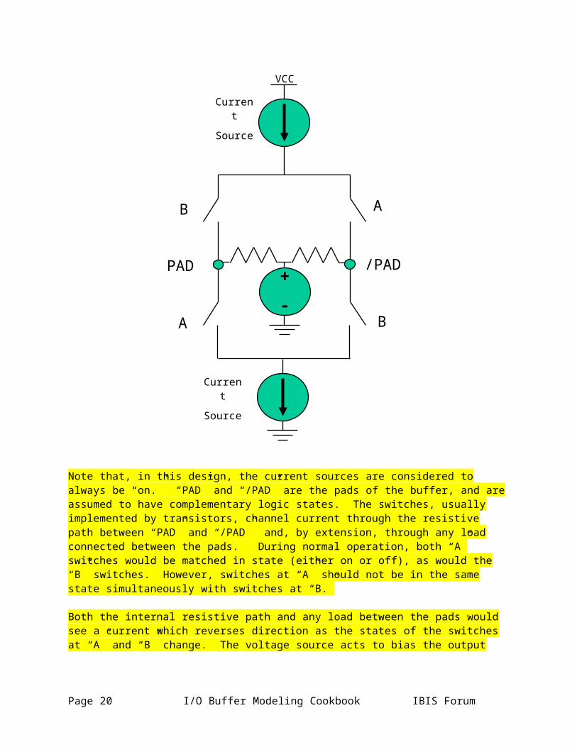
A true differential buffer resembles the following, conceptually.
Page 12 I/O Buffer Modeling Cookbook IBIS Forum
Note that, in this design, the current sources are considered to always be “on.” “PAD” and “/PAD” are the pads of the buffer, and are assumed to have complementary logic states. The switches, usually implemented by transistors, channel current through the resistive path between “PAD” and “/PAD” and, by extension, through any load connected between the pads. During normal operation, both “A” switches would be matched in state (either on or off), as would the “B” switches. However, switches at “A” should not be in the same state simultaneously with switches at “B.”
Both the internal resistive path and any load between the pads would see a current which reverses direction as the states of the switches at “A” and “B” change. The voltage source acts to bias the output waveform at a common mode voltage equal to that of the voltage source output.
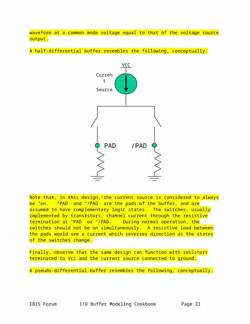
A half-differential buffer resembles the following, conceptually.
IBIS Forum I/O Buffer Modeling Cookbook Page 13
/PADPAD
CurrentSource
VCC
CurrentSource
+-
A
A B
B
Note that, in this design, the current source is considered to always be “on.” “PAD” and “/PAD” are the pads of the buffer, and are assumed to have complementary logic states. The switches, usually implemented by transistors, channel current through the resistive termination at “PAD” or “/PAD.” During normal operation, the switches should not be on simultaneously. A resistive load between the pads would see a current which reverses direction as the states of the switches change.
Finally, observe that the same design can function with resistors terminated to Vcc and the current source connected to ground.
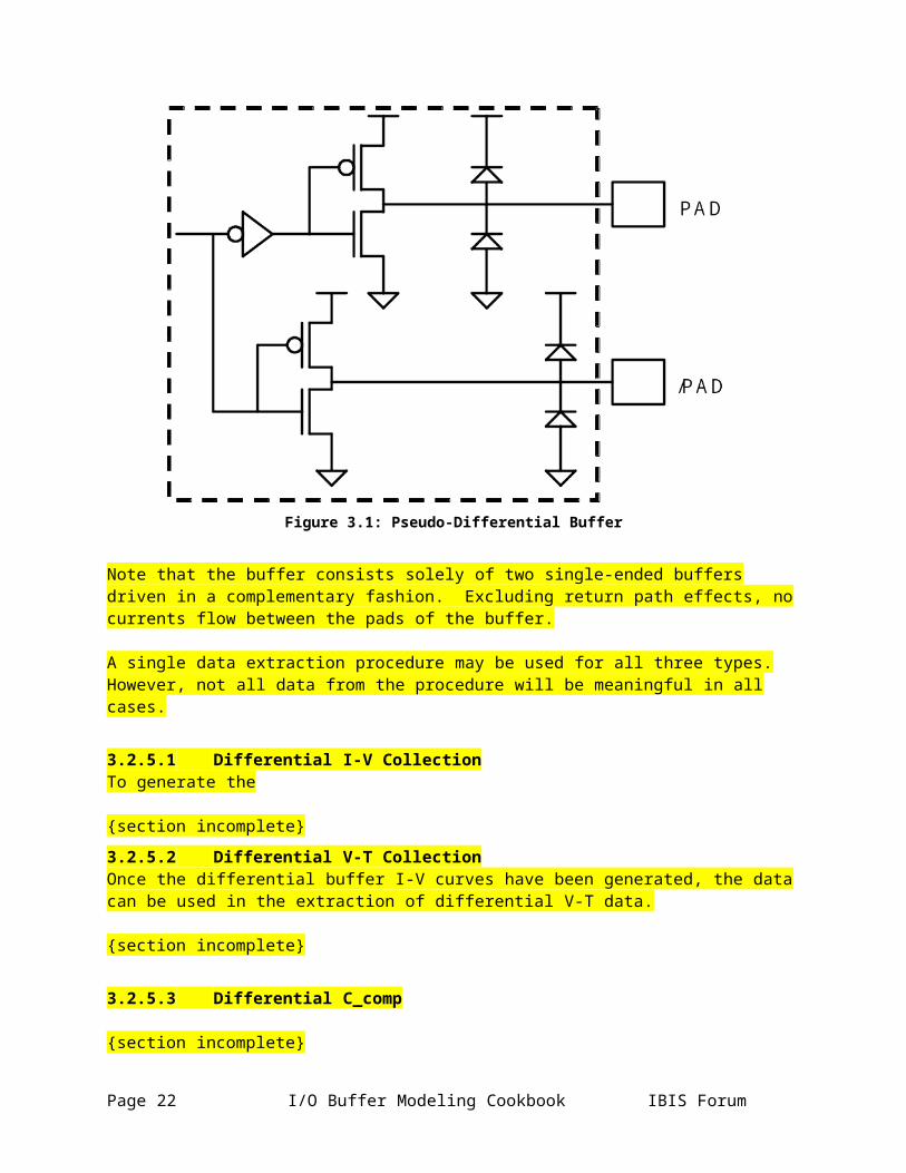
A pseudo-differential buffer resembles the following, conceptually.
Page 14 I/O Buffer Modeling Cookbook IBIS Forum
/PADPAD
CurrentSource
VCC
Figure 3.1: Pseudo-Differential Buffer
Note that the buffer consists solely of two single-ended buffers driven in a complementary fashion. Excluding return path effects, no currents flow between the pads of the buffer.
A single data extraction procedure may be used for all three types. However, not all data from the procedure will be meaningful in all cases.
3.2.5.1 Differential I-V CollectionTo generate the
{section incomplete}
3.2.5.2 Differential V-T CollectionOnce the differential buffer I-V curves have been generated, the data can be used in the extraction of differential V-T data.
{section incomplete}
3.2.5.3 Differential C_comp
{section incomplete}
3.3 Obtaining I-V and Switching Information via Lab MeasurmentYou can obtain I-V tables and rise/fall time information from the actual IC buffer, using the following lab setup:
IBIS Forum I/O Buffer Modeling Cookbook Page 15
• A programmable power supply with an output capable of sinking and sourcing current while maintaining the required output voltage. The output must be floating.
• A curve tracer• A digital sampling oscilloscope with at least a 4 GHz bandwidth• A low capacitance probe, e.g. FET• A test fixture used for DC measurements• A motherboard or specific test fixture used for transient measurements• If available, a thermoelectronic hot/cold plate (a peltier device), to control die temperature
To obtain I-V table measurements, mount the component to be tested under test (DUT) in the DC test fixture and connect the power and ground pins of the DUT to the programmable power supply. Attach the hot/cold plate to the device component with a very thin layer of thermal grease and adjust the temperature as desired. Wait for the die to stabilize at the desired temperature. Select an output on the DUT in the desired state (high or low) and use the curve tracer to obtain the I-V characteristics of the output.
NotesDuring curve tracing of a tri-statable output, the table contains both the transistor and the diode output characteristics. To obtain tables for the diodes alone, select and curve trace the output in its high impedance state.Device Buffers containing time-delayed feedback can produce bad results.
Reference the pullup and power clamp data to Vcc, as described in the IBIS specification. You can obtain this data directly by connecting the curve tracer’s negative (reference) lead to the Vcc supply of the DUT, then setting the curve tracer for a negative sweep. Make sure no ground path connects back through the AC line between the device component ground and power supply ground. For standard pulldown and clamp diode tables, attach the negative lead to the DUT’s GND supply and use a positive sweep direction. Ensure the supply is floating.
Note that the curve tracer may not be able to sweep the entire range required by the IBIS specifcation. In this case the model creator must extrapolate the tables to the required range. Capturing rise/fall time data requires either a specific test fixture or a motherboard to which the DUT can be attached. Rise/fall time measurements require an oscilloscope with at least a 4 GHz bandwidth. Take into account the effect on the rise/fall times of the device packaging and capacitive load. Use a probe with extremely low loading, i.e. 1 pf or less, such as a FET probe. The probe grounding should be less than 0.5 inches; i.e., don’t use the standard 6 inch probe grounds.
Take an oscilloscope picture of a buffer driving a known load. Then, using the known packaging parameters and measured I-V tables, construct a simulation model of the device buffer using a best guess of the rise/fall time. With an IBIS simulator, adjust the rise/fall times in the model until the simulation results match the oscilloscope waveforms. For greater control, lift the pin under test from any load other than the scope probe and simulate with a package and probe model.
Page 16 I/O Buffer Modeling Cookbook IBIS Forum
4.0 Putting the Data Into an IBIS FileBy this point, the user should have a set of data showing the behavior of the device buffer under a variety of environment and design conditions. The data set will include I-V (device buffer strength) and, where appropriate, V-T (device buffer speed) tables under several load types. The file may or may not include die capacitance information. The data must now be reformatted an IBIS model.The basic objective of any program that converts data to the IBIS format is to properly express the buffer’s behavior in a way “understandable” to IBIS-compatible tools. This involves several specific steps:
- basic syntax: representing the data under the proper IBIS keywords- data checking: making sure the data is not self-contradictory - data limiting: fitting the data within the IBIS size constraints- redundancy prevention: ensuring that design aspects are not improperly “double-counted”
under separate IBIS keywords
The following sections detail the specifics behind these steps.
The remainder of the document describes a bi-directional buffer – one capable of both driving a signal into a load and also receiving a signal from an outside world. However, many other buffer types exist; where appropriate, the differences in treatment needed for these other types will be described.The authors assume that the user is interested in either using a currently-available tool to convert data to IBIS format or is trying to perform this task himself. Several software tools exist to ease IBIS data conversions. These include:
- S2IBIS3 (SPICE2IBIS3, a free SPICE-based conversion tool)
These tools perform many or all of the steps described later in this document.
4.1 Basic Syntax: Keywords and Their DefinitionsAn IBIS file consists of three parts, with an optional ‘external’ package description. The three parts consist of
1. general information about the file itself and the component being modeled 2. the component’s name, pin-out and pin-to-buffer mapping3. behavioral descriptions of each unique buffer type in that component.
Note that an IBIS file can contain a description of more than one component (i.e. parts 2 and 3 can be repeated several times within one IBIS text file). For more information refer to the description of the [Component] keyword in the specification.
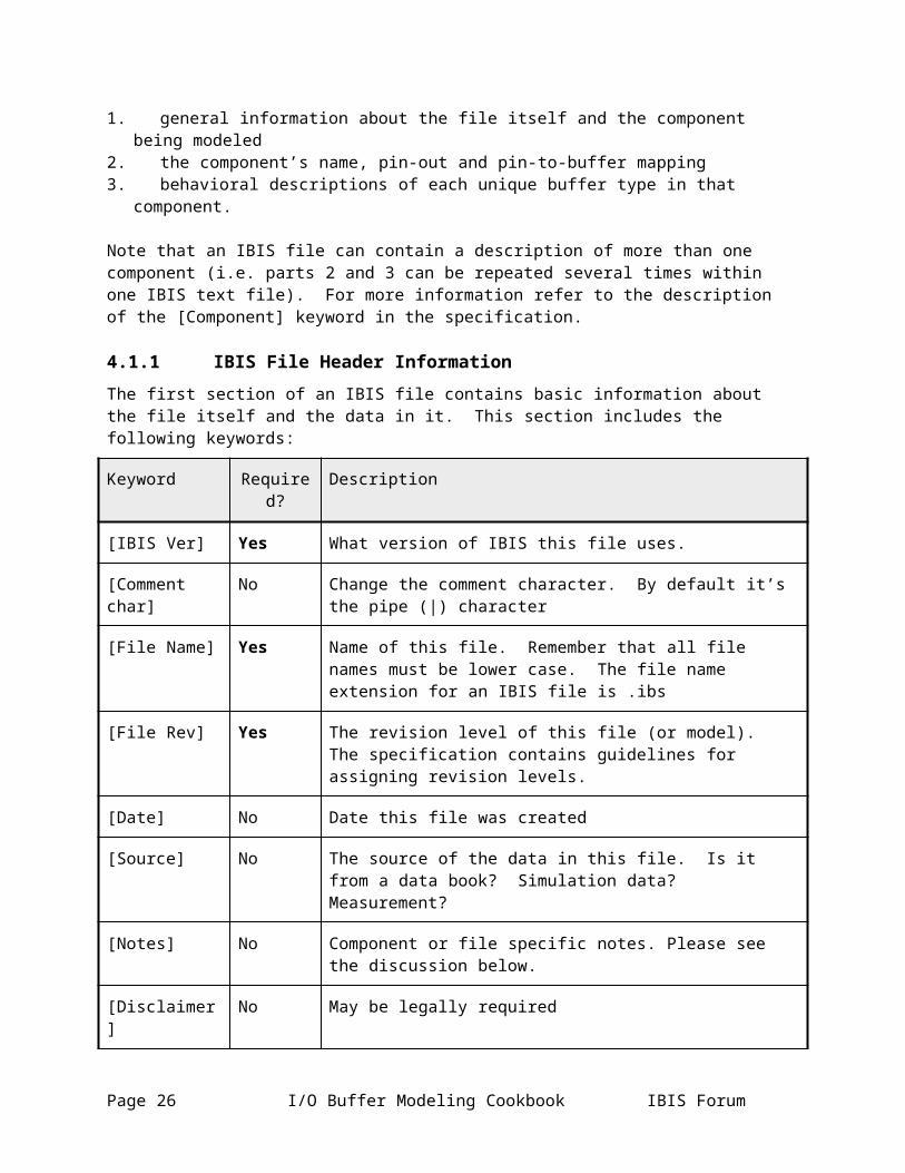
4.1.1 IBIS File Header InformationThe first section of an IBIS file contains basic information about the file itself and the data in it. This section includes the following keywords:
Keyword Required? Description
[IBIS Ver] Yes What version of IBIS this file uses.
[Comment char] No Change the comment character. By default it’s the pipe (|) character
IBIS Forum I/O Buffer Modeling Cookbook Page 17
[File Name] Yes Name of this file. Remember that all file names must be lower case. The file name extension for an IBIS file is .ibs
[File Rev] Yes The revision level of this file (or model). The specification contains guidelines for assigning revision levels.
[Date] No Date this file was created
[Source] No The source of the data in this file. Is it from a data book? Simulation data? Measurement?
[Notes] No Component or file specific notes. Please see the discussion below.
[Disclaimer] No May be legally required
[Copyright] No The files copyright notice
The use of these keywords is self-explanatory. Note that while the [Date], [Source], etc. keywords are not required, there use is strongly recommended. The [Notes] keyword is especially valuable, in that the model creator can include in the IBIS file such information as:
Specific model and simulator use information. For example, if the file is marked as IBIS revision 2.1 the [Notes] keyword may specify what specific 2.1 features a simulator must support. Specific model use requirements or caveats may also be described here.
Information on SSO conditions. Under what switching conditions (i.e. how many SSO’s) were the minimum, typical and maximum corners derived? Was the device buffer’s Tco taken under the same conditions (it should be)?
Additional package modeling information may be included
The models validation level may also be described
4.1.2 Component and Pin Information
This section of an IBIS file is where the ‘data book’ information regarding the device component’s pinout, pin to buffer mapping, and the devices package and pin electrical parameters are placed.
Keyword Required? Description
[Component] Yes The name of the component being modeled. Standard practice has been to use the industry standard part designation.
[Manufacture] Yes The name of the component manufacturer
[Package] Yes This keyword contains the range (minimum, typical and maximum values) over which the packages’ lead resistance, inductance and
Page 18 I/O Buffer Modeling Cookbook IBIS Forum
capacitance vary (the R_pkg, L_pkg and C_Pkg parameters).
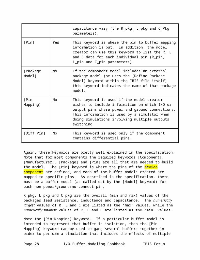
[Pin] Yes This keyword is where the pin to buffer mapping information is put. In addition, the model creator can use this keyword to list the R, L and C data for each individual pin (R_pin, L_pin and C_pin parameters).
[Package Model] No If the component model includes an external package model (or uses the [Define Package Model] keyword within the IBIS file itself) this keyword indicates the name of that package model.
[Pin Mapping] No This keyword is used if the model creator wishes to include information on which I/O or output pins share power and ground connections. This information is used by a simulator when doing simulations involving multiple outputs switching
[Diff Pin] No This keyword is used only if the component contains differential pins.
Again, these keywords are pretty well explained in the specification. Note that for most components the required keywords [Component], [Manufacturer], [Package] and [Pin] are all that are needed to build the model. The [Pin] keyword is where the pins of the device component are defined, and each of the buffer models created are mapped to specific pins. As described in the specification, there must be a buffer model (as called out by the [Model] keyword) for each non power/ground/no-connect pin.
R_pkg, L_pkg and C_pkg are the overall (min and max) values of the packages lead resistance, inductance and capacitance. The numerically largest values of R, L and C are listed as the ‘max’ values, while the numerically smallest values of R, L and C are listed as the ‘min’ values.
Note the [Pin Mapping] keyword. If a particular buffer model is intended to represent that buffer in isolation, then the [Pin Mapping] keyword can be used to gang several buffers together in order to perform a simulation that includes the effects of multiple outputs switching. If the model is intended to be used with the [Pin Mapping] keyword information then that should be noted in the [Notes] section. Note however that not all simulators support this feature.
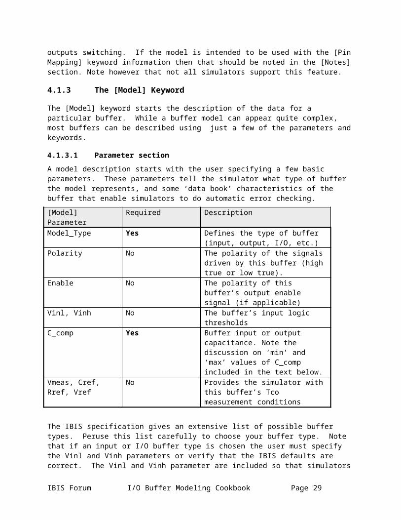
4.1.3 The [Model] Keyword
The [Model] keyword starts the description of the data for a particular buffer. While a buffer model can appear quite complex, most buffers can be described using just a few of the parameters and keywords.
4.1.3.1 Parameter section
A model description starts with the user specifying a few basic parameters. These parameters tell the simulator what type of buffer the model represents, and some ‘data book’ characteristics of the buffer that enable simulators to do automatic error checking.
[Model] Parameter Required DescriptionModel_Type Yes Defines the type of buffer (input, output,
I/O, etc.)Polarity No The polarity of the signals driven by this
buffer (high true or low true).Enable No The polarity of this buffer’s output enable
IBIS Forum I/O Buffer Modeling Cookbook Page 19
signal (if applicable)Vinl, Vinh No The buffer’s input logic thresholdsC_comp Yes Buffer input or output capacitance. Note
the discussion on ‘min’ and ‘max’ values of C_comp included in the text below.
Vmeas, Cref, Rref, Vref No Provides the simulator with this buffer’s Tco measurement conditions
The IBIS specification gives an extensive list of possible buffer types. Peruse this list carefully to choose your buffer type. Note that if an input or I/O buffer type is chosen the user must specify the Vinl and Vinh parameters or verify that the IBIS defaults are correct. The Vinl and Vinh parameter are included so that simulators can flag signal integrity violations and perform timing calculations. In addition, all output or I/O type buffer models should include the Vmeas, Cref, Rfer and Vref parameters. Including these parameters allows a simulator to do board level timing calculations.
The C_comp parameter specifies the buffer’s input, output or I/O capacitance and can have a typical, minimum and maximum value. Note that when constructing the IBIS file the numerically largest value of C_comp is listed as the ‘max’ value while the numerically smallest value of C_comp is listed as the ‘min’ value. C_comp min and max values do not necessarily correlate with the min and max conditions under which the I-V and switching data was gathered. C_comp represents only the capacitance of the transistors, die pad and interconnect for an individual buffer. It does not include package capacitance.
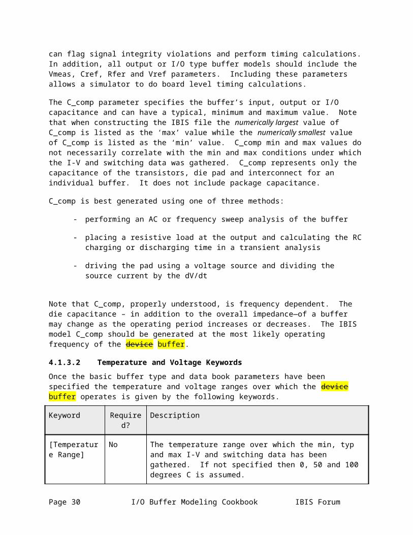
C_comp is best generated using one of three methods:
- performing an AC or frequency sweep analysis of the buffer
- placing a resistive load at the output and calculating the RC charging or discharging time in a transient analysis
- driving the pad using a voltage source and dividing the source current by the dV/dt
Note that C_comp, properly understood, is frequency dependent. The die capacitance – in addition to the overall impedance—of a buffer may change as the operating period increases or decreases. The IBIS model C_comp should be generated at the most likely operating frequency of the device buffer.
4.1.3.2 Temperature and Voltage Keywords
Once the basic buffer type and data book parameters have been specified the temperature and voltage ranges over which the device buffer operates is given by the following keywords.
Keyword Required? Description
[Temperature Range]
No The temperature range over which the min, typ and max I-V and switching data has been gathered. If not specified then 0, 50 and 100 degrees C is assumed.
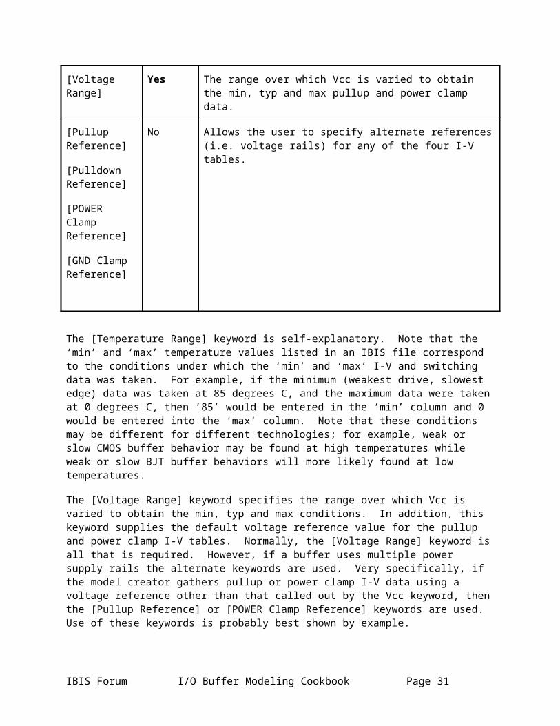
[Voltage Range] Yes The range over which Vcc is varied to obtain the min, typ and max pullup and power clamp data.
Page 20 I/O Buffer Modeling Cookbook IBIS Forum
[Pullup Reference]
[Pulldown Reference]
[POWER Clamp Reference]
[GND Clamp Reference]
No Allows the user to specify alternate references (i.e. voltage rails) for any of the four I-V tables.
The [Temperature Range] keyword is self-explanatory. Note that the ‘min’ and ‘max’ temperature values listed in an IBIS file correspond to the conditions under which the ‘min’ and ‘max’ I-V and switching data was taken. For example, if the minimum (weakest drive, slowest edge) data was taken at 85 degrees C, and the maximum data were taken at 0 degrees C, then ’85’ would be entered in the ‘min’ column and 0 would be entered into the ‘max’ column. Note that these conditions may be different for different technologies; for example, weak or slow CMOS buffer behavior may be found at high temperatures while weak or slow BJT buffer behaviors will more likely found at low temperatures.
The [Voltage Range] keyword specifies the range over which Vcc is varied to obtain the min, typ and max conditions. In addition, this keyword supplies the default voltage reference value for the pullup and power clamp I-V tables. Normally, the [Voltage Range] keyword is all that is required. However, if a buffer uses multiple power supply rails the alternate keywords are used. Very specifically, if the model creator gathers pullup or power clamp I-V data using a voltage reference other than that called out by the Vcc keyword, then the [Pullup Reference] or [POWER Clamp Reference] keywords are used. Use of these keywords is probably best shown by example.
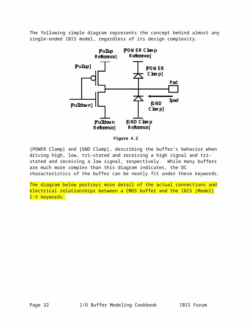
The following simple diagram represents the concept behind almost any single-ended IBIS model, regardless of its design complexity.
IBIS Forum I/O Buffer Modeling Cookbook Page 21
Figure 4.2
[POWER Clamp] and [GND Clamp], describing the buffer’s behavior when driving high, low, tri-stated and receiving a high signal and tri-stated and receiving a low signal, respectively. While many buffers are much more complex than this diagram indicates, the DC characteristics of the buffer can be neatly fit under these keywords.
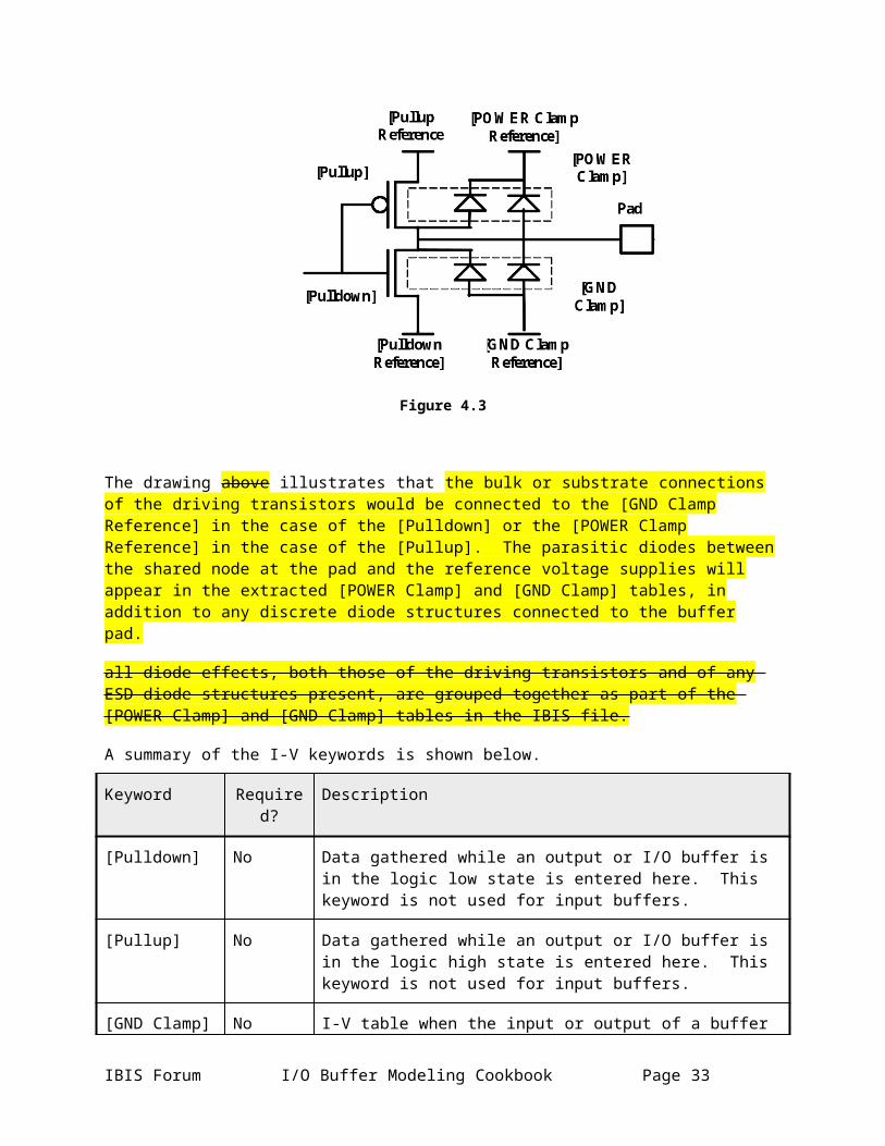
The diagram below portrays more detail of the actual connections and electrical relationships between a CMOS buffer and the IBIS [Model] I-V keywords.
Figure 4.3
The drawing above illustrates that the bulk or substrate connections of the driving transistors would be connected to the [GND Clamp Reference] in the case of the [Pulldown] or the [POWER Clamp
Page 22 I/O Buffer Modeling Cookbook IBIS Forum
Reference] in the case of the [Pullup]. The parasitic diodes between the shared node at the pad and the reference voltage supplies will appear in the extracted [POWER Clamp] and [GND Clamp] tables, in addition to any discrete diode structures connected to the buffer pad.
all diode effects, both those of the driving transistors and of any ESD diode structures present, are grouped together as part of the [POWER Clamp] and [GND Clamp] tables in the IBIS file.
A summary of the I-V keywords is shown below.
Keyword Required? Description
[Pulldown] No Data gathered while an output or I/O buffer is in the logic low state is entered here. This keyword is not used for input buffers.
[Pullup] No Data gathered while an output or I/O buffer is in the logic high state is entered here. This keyword is not used for input buffers.
[GND Clamp] No I-V table when the input or output of a buffer is driven below ground (or the reference specified by the [GND Clamp Reference] keyword
[POWER Clamp]
No I-V table when the input or output of a buffer is driven above Vcc (or the reference specified by the [POWER Clamp Reference] keyword
The first thing one notices is that, strictly speaking, none of the four I-V tables are mandatory. Non 3-state buffers (i.e. buffers where one cannot isolate separate power and ground clamp diode effect) require only the [Pulldown] and [Pullup] keywords. Input buffers use only the [GND Clamp] and [POWER Clamp] keywords. 3-state buffers require all four keywords. Open drain/collector buffers can make the current data in the [Pullup] table all zeros, or omit the [Pullup] keyword altogether. Each keyword is followed by a set of data in tabular format. Enter the gathered I-V data into the appropriate tables. The rules for constructing the I-V tables are as follows:
4.1.3.3 Pulldown
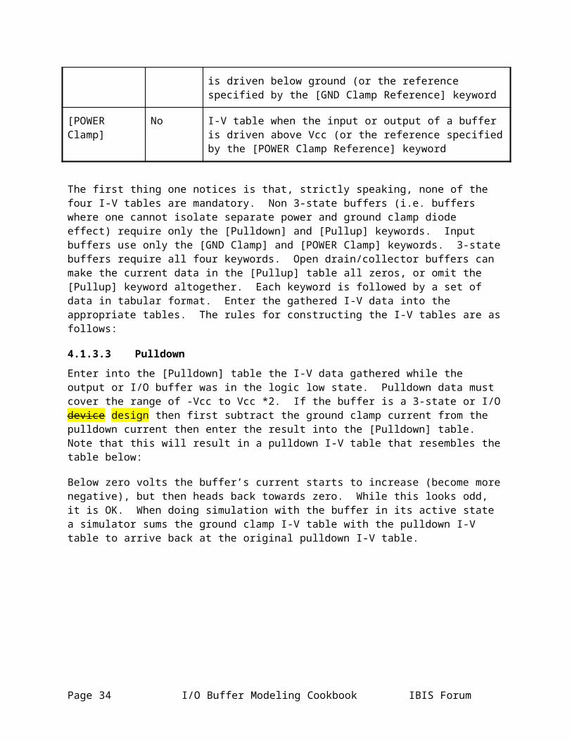
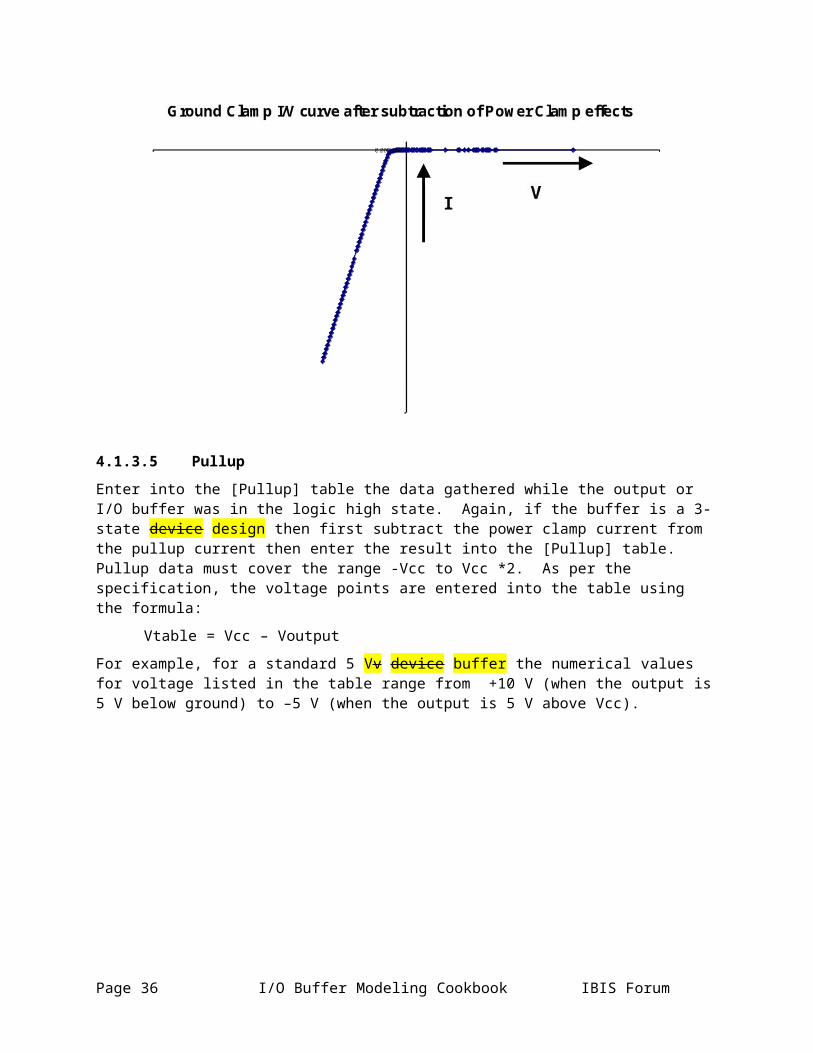
Enter into the [Pulldown] table the I-V data gathered while the output or I/O buffer was in the logic low state. Pulldown data must cover the range of -Vcc to Vcc *2. If the buffer is a 3-state or I/O device design then first subtract the ground clamp current from the pulldown current then enter the result into the [Pulldown] table. Note that this will result in a pulldown I-V table that resembles the table below:
Below zero volts the buffer’s current starts to increase (become more negative), but then heads back towards zero. While this looks odd, it is OK. When doing simulation with the buffer in its active state a simulator sums the ground clamp I-V table with the pulldown I-V table to arrive back at the original pulldown I-V table.
IBIS Forum I/O Buffer Modeling Cookbook Page 23
4.1.3.4 Ground Clamp
Enter into the [GND Clamp] table the ground clamp I-V data. For I/O buffers this is the ground relative data gathered while the buffer was in the high impedance state. The data in table must cover the range of -Vcc to Vcc, though power clamp effects must be removed from the data appearing under the [GND Clamp] keyword in the final IBIS model.
Page 24 I/O Buffer Modeling Cookbook IBIS Forum
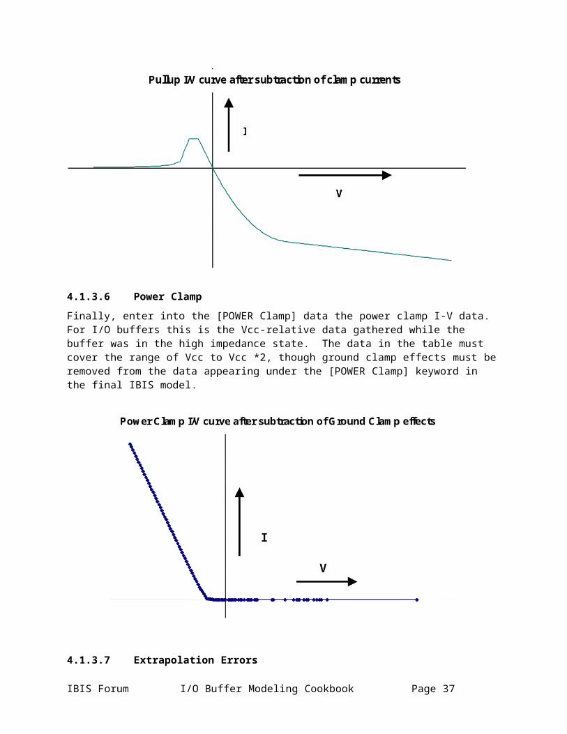
4.1.3.5 Pullup
Enter into the [Pullup] table the data gathered while the output or I/O buffer was in the logic high state. Again, if the buffer is a 3-state device design then first subtract the power clamp current from the pullup current then enter the result into the [Pullup] table. Pullup data must cover the range -Vcc to Vcc *2. As per the specification, the voltage points are entered into the table using the formula:
Vtable = Vcc – Voutput
For example, for a standard 5 Vv device buffer the numerical values for voltage listed in the table range from +10 V (when the output is 5 V below ground) to –5 V (when the output is 5 V above Vcc).
4.1.3.6 Power Clamp
Finally, enter into the [POWER Clamp] data the power clamp I-V data. For I/O buffers this is the Vcc-relative data gathered while the buffer was in the high impedance state. The data in the table must cover the range of Vcc to Vcc *2, though ground clamp effects must be removed from the data appearing under the [POWER Clamp] keyword in the final IBIS model.
IBIS Forum I/O Buffer Modeling Cookbook Page 25
4.1.3.7 Extrapolation Errors
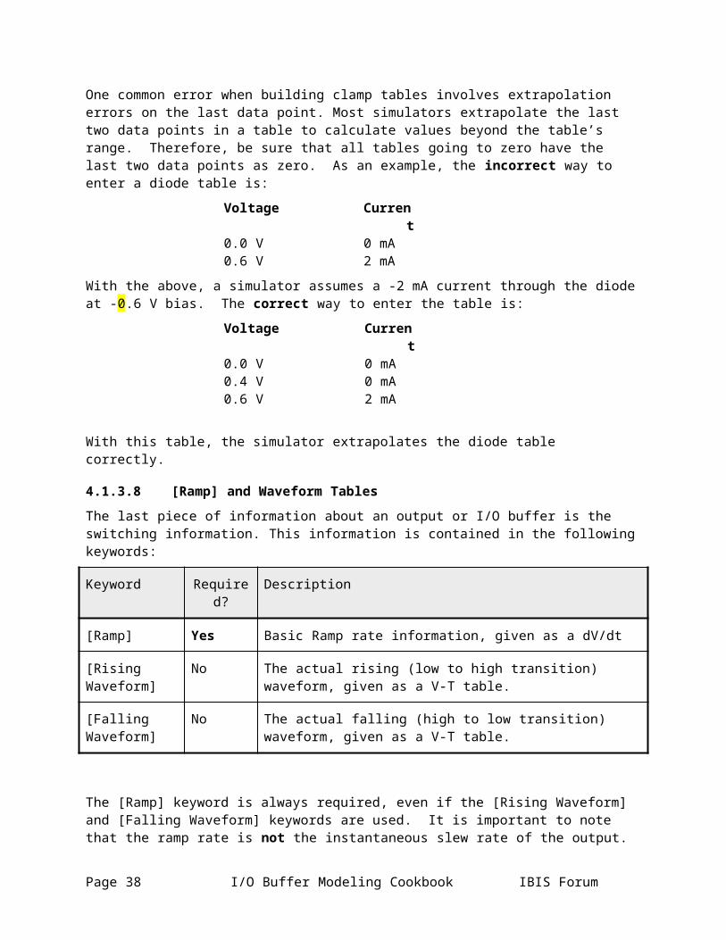
One common error when building clamp tables involves extrapolation errors on the last data point. Most simulators extrapolate the last two data points in a table to calculate values beyond the table’s range. Therefore, be sure that all tables going to zero have the last two data points as zero. As an example, the incorrect way to enter a diode table is:
Voltage Current0.0 V 0 mA0.6 V 2 mA
With the above, a simulator assumes a -2 mA current through the diode at -0.6 V bias. The correct way to enter the table is:
Voltage Current0.0 V 0 mA0.4 V 0 mA0.6 V 2 mA
With this table, the simulator extrapolates the diode table correctly.
4.1.3.8 [Ramp] and Waveform Tables
The last piece of information about an output or I/O buffer is the switching information. This information is contained in the following keywords:
Keyword Required? Description
[Ramp] Yes Basic Ramp rate information, given as a dV/dt
[Rising Waveform]
No The actual rising (low to high transition) waveform, given as a V-T table.
Page 26 I/O Buffer Modeling Cookbook IBIS Forum
[Falling Waveform]
No The actual falling (high to low transition) waveform, given as a V-T table.
The [Ramp] keyword is always required, even if the [Rising Waveform] and [Falling Waveform] keywords are used. It is important to note that the ramp rate is not the instantaneous slew rate of the output. Instead, it is a number that indicates how long it takes the output transistor structures to switch from one state to another. As such, the dV portion of the [Ramp] keyword data is specified to cover the 20% to 80% voltage swing of the output. Specifically, the “ramp rate” as posted in an IBIS file is defined as:
Do not reduce dV/dt to a single number.
4.1.3.9 Keywords and Specific Buffer Types
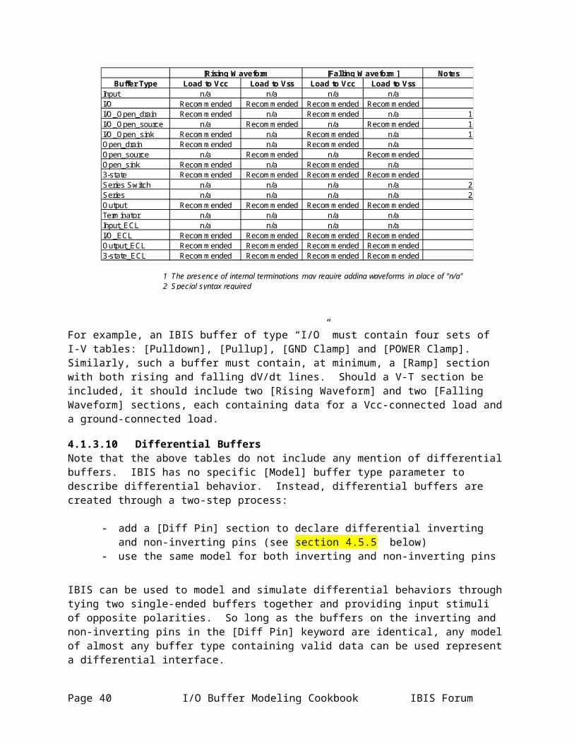
The IBIS standard allows a variety of buffer types to be described with I-V and V-T tables. While the specification is flexible in which tables may be included under any keyword, the following table shows the minimum recommended data for any buffer type.
Data under "n/a" keywords may be included, if the current is set equal to 0.Functionally similar to "I/OSpecial syntax requiredClamp data may be included, but is added to the required data when the buffer drives
Strictly speaking, V-T tables are not required under the IBIS specification. However, for accurate modeling, certain combinations of tables are recommended. These are described in the table below.
IBIS Forum I/O Buffer Modeling Cookbook Page 27
NotesBuffer Type Load to Vcc Load to Vss Load to Vcc Load to Vss
The presence of internal terminations may require adding waveforms in place of "n/a"Special syntax required
For example, an IBIS buffer of type “I/O” must contain four sets of I-V tables: [Pulldown], [Pullup], [GND Clamp] and [POWER Clamp]. Similarly, such a buffer must contain, at minimum, a [Ramp] section with both rising and falling dV/dt lines. Should a V-T section be included, it should include two [Rising Waveform] and two [Falling Waveform] sections, each containing data for a Vcc-connected load and a ground-connected load.
4.1.3.10 Differential BuffersNote that the above tables do not include any mention of differential buffers. IBIS has no specific [Model] buffer type parameter to describe differential behavior. Instead, differential buffers are created through a two-step process:
- add a [Diff Pin] section to declare differential inverting and non-inverting pins (see section 4.5.5 below)
- use the same model for both inverting and non-inverting pins
IBIS can be used to model and simulate differential behaviors through tying two single-ended buffers together and providing input stimuli of opposite polarities. So long as the buffers on the inverting and non-inverting pins in the [Diff Pin] keyword are identical, any model of almost any buffer type containing valid data can be used represent a differential interface.
For example, if a differential driver were to be created and one has single-ended buffer data for the model “TESTMODEL,” one would begin by creating two pins on the device in the [Pin] list, each using the model “TESTMODEL.” The [Diff Pin] section of the IBIS file would show one of these pins as an inverting output and the other as the non-inverting output.
When a simulation is to be performed, so long as the two “TESTMODEL” buffers are provided with input signals which are opposite in polarity, the buffers will act in a differential fashion. Many simulation tools will ensure opposing polarities of input waveforms automatically if the [Diff Pin] keyword is present.
Page 28 I/O Buffer Modeling Cookbook IBIS Forum
{section incomplete}
If the differential data collection procedures mentioned above were followed, a differential C_comp may be expressed using the [C Series] keyword described below.
4.2 Data CheckingSeveral data checks are critical to assure final IBIS models that are useful in simulation:
- data completeness- I-V and V-T matching
4.2.1 Data CompletenessFundamentally, data completeness means having sufficient data to create a useful IBIS model. Users should ensure that the data in their raw data files includes:
- I-V data covering –Vcc to 2*Vcc for all corners- I-V data covering sufficient data points to describe buffer behavior- I-V data showing behavior for all appropriate input states (high, low, high-Z)- V-T data covering sufficient data points to describe buffer behavior- V-T data (where appropriate) showing complete transitions (settled low to settled high)- V-T data (where appropriate) showing two to four or more transitions into a load
See Chapter 3 for more information on generating complete data.
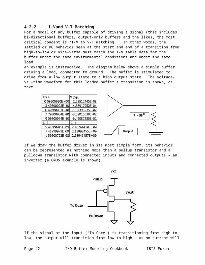
4.2.2 I-Vand V-T MatchingFor a model of any buffer capable of driving a signal (this includes bi-directional buffers, output-only buffers and the like), the most critical concept is “I-V to V-T matching.” In other words, the settled or DC behavior seen at the start and end of a transition from high-to-low or vice-versa must match the I-V table data for the buffer under the same environmental conditions and under the same load.An example is instructive. The diagram below shows a simple buffer driving a load, connected to ground. The buffer is stimulated to drive from a low output state to a high output state. The voltage-vs.-time waveform for this loaded buffer’s transition is shown, as text.
Time V(typ)0.00000000E+00 2.29512445E-083.40000028E-10 4.38917952E-046.40000053E-10 -1.97395235E-027.70000064E-10 -3.52016538E-029.00000074E-10 -6.49087280E-02
If we draw the buffer driver in its most simple form, its behavior can be represented as nothing more than a pullup transistor and a pulldown transistor with connected inputs and connected outputs – an inverter (a CMOS example is shown).
IBIS Forum I/O Buffer Modeling Cookbook Page 29
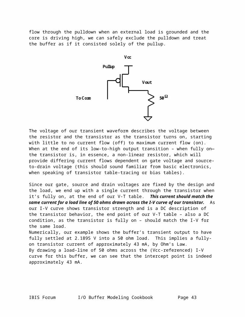
If the signal at the input (“To Core”) is transitioning from high to low, the output will transition from low to high. As no current will flow through the pulldown when an external load is grounded and the core is driving high, we can safely exclude the pulldown and treat the buffer as if it consisted solely of the pullup.
The voltage of our transient waveform describes the voltage between the resistor and the transistor as the transistor turns on, starting with little to no current flow (off) to maximum current flow (on). When at the end of its low-to-high output transition – when fully on—the transistor is, in essence, a non-linear resistor, which will provide differing current flows dependent on gate voltage and source-to-drain voltage (this should sound familiar from basic electronics, when speaking of transistor table-tracing or bias tables).
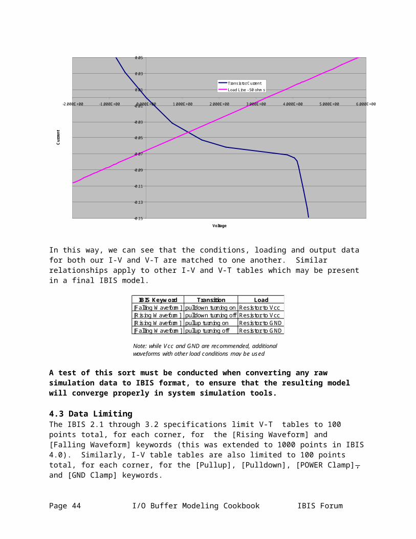
Since our gate, source and drain voltages are fixed by the design and the load, we end up with a single current through the transistor when it’s fully on, at the end of our V-T table. This current should match the same current for a load line of 50 ohms drawn across the I-V curve of our transistor. As our I-V curve shows transistor strength and is a DC description of the transistor behavior, the end point of our V-T table – also a DC condition, as the transistor is fully on – should match the I-V for the same load.Numerically, our example shows the buffer’s transient output to have fully settled at 2.1895 V into a 50 ohm load. This implies a fully-on transistor current of approximately 43 mA, by Ohm’s Law.By drawing a load-line of 50 ohms across the (Vcc-referenced) I-V curve for this buffer, we can see that the intercept point is indeed approximately 43 mA.
In this way, we can see that the conditions, loading and output data for both our I-V and V-T are matched to one another. Similar relationships apply to other I-V and V-T tables which may be present in a final IBIS model.
IBIS Keyword Transition Load[Falling Waveform] pulldown turning on Resistor to Vcc[Rising Waveform] pulldown turning off Resistor to Vcc[Rising Waveform] pullup turning on Resistor to GND[Falling Waveform] pullup turning off Resistor to GND
Note: while Vcc and GND are recommended, additionalwaveforms with other load conditions may be used
A test of this sort must be conducted when converting any raw simulation data to IBIS format, to ensure that the resulting model will converge properly in system simulation tools.
4.3 Data LimitingThe IBIS 2.1 through 3.2 specifications limit V-T tables to 100 points total, for each corner, for the [Rising Waveform] and [Falling Waveform] keywords (this was extended to 1000 points in IBIS 4.0). Similarly, I-V table tables are also limited to 100 points total, for each corner, for the [Pullup], [Pulldown], [POWER Clamp], and [GND Clamp] keywords.
These limitations mean that some sort of algorithm must be used to select which points from the raw data file are used in the final IBIS model, should the data file contain more than 100 points per corner. Two methods are now in use:
- Points selected using a regular interval- Points selected using “greatest change” algorithm
IBIS Forum I/O Buffer Modeling Cookbook Page 31
The first of these simply “picks” data points at regular intervals over the data set. For example, in a V-T table data set containing 200 points, from 0 ns to 199 ns, the limitation could be met by selecting only even data points plus zero; the sequence would then be 0 ns, 2 ns, and so on.
While this method is simple to implement, it does not discriminate between “meaningful” and “meaningless” data points. If a V-T table has settled by the 50th used data point, the remaining data points will still be selected and added to the IBIS file, though the voltage information will not change.
This failing is remedied by use of a “greatest change” algorithm, which selects data points on the basis of first derivative. In this way, more points in the final IBIS file will be expended on areas of the tables where large changes take place, such as inflections. Few points will be used on areas where the output does not change, such as the settled voltages before and after a V-T transition.
A visual example follows.
Note that the 100-point restriction applies to the number of voltage points in the I-V tables and, for revision 2.1 through 3.2 models, the time points in the V-T tables. Not all I-V current points or V-T voltage points need to be used in the tables. If necessary, the keyword “NA” may be inserted in the I-V tables for points in any of the corners. The only restrictions on the use of “NA” are:
- at least one corner must contain a legitimate current point for any I-V voltage point
- at least one corner must contain a legitimate voltage point for any V-T time point
- the starting and ending points for the typical corner in the V-T and I-V tables cannot use the “NA” reserved word
Page 32 I/O Buffer Modeling Cookbook IBIS Forum
4.4 Redundancy Prevention
The IBIS specification splits the I-V behavior of a buffer into several categories: [Pullup], [Pulldown], etc. However, the actual data obtained from simulation or from laboratory experiments may not be so easily divided between different conceptual portions of a buffer design.
I-V tables require two kinds of adjustment in order to ensure that buffer behavioral data is properly partitioned between I-V tables:
- Clamp “cutting”
- Adjustment of model data for internal terminations
- V-T table “cutting”
When a buffer is either tri-stated or placed in input mode and then curve-traced referenced to ground, a curve similar to the following will result.
Note that two diode effects are shown – the ground clamp, which appears below 0 V and the power clamp, which appears above 4 V. Before this data can appear in an IBIS model under the [POWER Clamp] and [GND Clamp] keywords, the diode tables must be split apart.
If no internal termination is present, the splitting is fairly simple: the ground clamp will be created by cutting the table at 0 V and extending the current seen at 0 V up to 2 * Vcc.
Internal parallel terminations can affect all four tables of a bidirectional (I/O) buffer model. Most commonly, these terminations are implemented through the use of extra devices structures on-die which
Page 34 I/O Buffer Modeling Cookbook IBIS Forum
act as resistors, always connected to Vcc or ground regardless of whether the device buffer drives or receives.
Since the clamp tables are used in an I/O buffer both when driving and receiving, such terminations are best included as part of a clamp table. More specifically, ground terminations would be included with [GND clamp] data and Vcc terminations with [POWER Clamp] data.
The resistor’s effect would be to make the buffer operating region, which is normally at 0 mA in a clamp table, show a slope equal to the value of the resistor used.
A specific example will help to illustrate the idea. If a buffer contains an internal ground termination, it can be modeled as shown in the next diagram.
Since the [Pullup] and [Pulldown] tables will be created by subtracting the clamp data from the transistor data, then the resistor effects should not appear in these sections and no adjustment to them is necessary. The only change needed to the raw data is to make sure that the resistor’s effects are not “double-counted” with the [POWER Clamp] in addition to the [GND Clamp]. The easiest way to accomplish this is by adjusting the power clamp data before it is clipped for inclusion in the IBIS model.
IBIS Forum I/O Buffer Modeling Cookbook Page 35
Clamps - Raw (Edited IDE)
-2.00E-03
-1.50E-03
-1.00E-03
-5.00E-04
0.00E+00
5.00E-04
1.00E-03
1.50E-03
2.00E-03
-2 -1 0 1 2 3 4 5 6 7
Voltage (v)
Cur
rent
(A)
i_gndclampi_vccclamp
The above diagram shows the raw clamp data taken from simulation or the laboratory. To eliminate the resistor’s effects, the power clamp curve should be shifted to cross through the zero volts, zero amps axis. Both curves can then be clipped as described earlier in the chapter. The resulting data can then be used in the IBIS model.
-2.00E-03
-1.50E-03
-1.00E-03
-5.00E-04
0.00E+00
5.00E-04
1.00E-03
1.50E-03
2.00E-03
-2 -1 0 1 2 3 4 5 6 7
Voltage (v)
Cur
rent
(A) i_gndclamp
i_vccclamp_originali_gndclamp_originali_vccclamp
Page 36 I/O Buffer Modeling Cookbook IBIS Forum
A similar procedure should be followed for Vcc-connected terminations. Other termination types (only on when receiving, only on when driving or receiving specific signal levels) require advanced keywords, as detailed later in the chapter.
One procedure which is not performed by most automated IBIS creation tools is V-T table clipping. While there is no upper limit on the time duration of V-T tables, the transient portion of the waveforms must start and finish within the time dictated by the highest frequency of the buffer (one-half of the period). Several software suites that can accept IBIS models improperly use V-T table data, allowing settled portions to distort buffer behavior when the buffer is driven at higher frequencies.
While not an IBIS requirement, users are strongly recommended to generate V-T tables that are shorter in duration than the pulse width of the highest frequency anticipated on the interface. For example, a signal that is anticipated to drive, at maximum, 100 MHz signals should have a V-T table duration no greater than 5 ns (the period of a 100 MHz signal is 10 ns; such a signal’s pulse width – longest “high time” or longest “low time” – is 5 ns).
4.5 Advanced Keywords and Constructs
Several keywords exist for describing more complex behaviors. The most common of these are described below:
The [Model Selector] keyword is a simple means by which several buffers can be made optionally available for simulation at the same physical pin of the device component. Normally, each pin of an IBIS pin list references only one buffer, as shown below.
In this example, each pin has a unique pin name and separately references a particular buffer, found later in the file.
[Model Selector] allows a family of buffers to be “attached” to the same pin. The IBIS specification assumes that the simulation tool using the IBIS file will give the user an option of selection which individual buffer within the family will be selected for use in any particular case.
Here, the names of the [Model Selector] families are substituted in the pin list for the buffer names we would usually expect to see. Later in the file, a [Model Selector] keyword is used, followed by the individual buffers that are part of that selector and a short comment or description of that buffer’s function. In this example, a user interested in simulating with pin “AA21” would have to select, through his simulation tool, which of the individual buffers under the [Model Selector] “buff_selector_in” he wishes to use in his simulation.
There is little to no restriction on how many buffers or what buffer types can be used in a particular [Model Selector] section.
4.5.2 [Submodel]
The [Submodel] keyword is used to enable additional buffer features under certain conditions. This is most commonly used to activate additional clamping circuitry when a bi-directional buffer is receiving, but prevent this circuitry from becoming active when the circuit drives. As the [POWER Clamp] and [GND Clamp] data is present during both driving and receiving states, [Submodel] allows extra driving or clamping behaviors to be described for only some buffer conditions.
An example best illustrates [Submodel] usage. Imagine an interface with parallel termination at the receiver. The termination is provided by the buffer itself, by leaving the pulldown transistor on when the buffer is receiving; however, the termination is inactive when the buffer drives. By using a dynamic clamp [Submodel] [GND Clamp], the termination can be included in receiving simulations automatically, without affecting the driver behavior.
The Submodel is called by using the [Add Submodel] keyword. The name and mode of operation must be identified under the [Add Submodel] call. Receiver clamps use the “Non-Driving” mode.
|**************************************************************************[Add Submodel]|Submodel name Mode
The [Submodel] itself is created for this buffer by copying the IBIS [Pulldown] table data exactly and relabeling it as a [GND Clamp]. The [Submodel]’s name must be included here and must match the [Add Submodel] call. Finally, the Submodel_type must be specified; as the termination is a clamp which is active only when the buffer receives, the type is “Dynamic_clamp.”
The IBIS specification permits users to describe high and low input thresholds, buffer delay fixtures and delay measurement voltages. These values are given under the [Model] keyword, using the Vinh, Vinl, Cref, Vref, Rref and Vmeas parameters, respectively. In some designs, however, the values for these parameters change with corner or supply voltage. The [Model Spec] keyword allows the variations for these parameters to be described in the “typ,” “min,” and “max” format used elsewhere in the model.
In the example below, Vmeas, Vinh and Vinl levels are specified for each of the three model corners.
|***************************************************************************|[Model] standard_bufferModel_type I/O|Vinl = 0.99VVinh = 1.65VCref = 10.000pFRref = 25.0OhmVref = 0.000V|| typ min maxC_comp 3.350pF 3.280pF 3.440pF[Model Spec]
Some applications require that a buffer change its strength or transition speed characteristics at fixed times after input stimulus changes. For example, a buffer may employ a “kicker” or boosted drive strength on its pullup behavior for the first few nanoseconds after a low-to-high transition. Since the buffer effectively has two drive strengths, no single set of I-V and V-T tables can effectively describe its behavior. The [Driver Schedule] keyword enables a buffer model to use or combine the behaviors of several individual models.
The keyword is itself part of a model, usually called the “top-level” model. The parameters of the keyword form a list of the models whose behavior the top-level model schedules (The top-level model is required for the benefit of simulation tools which cannot support the [Driver Schedule] behavior). Each incorporated model can include up to four delay parameters, expressing the delay for pullup and pulldown behavior turning off or on after a rising or falling edge.
|***************************************************************************|[Model] GTL_exampleModel_type I/O|Vinl = 800.00mVVinh = 1.20VVmeas = 1.00VVref = 1.50VRref = 50.00OhmCref = 0.00pF|| typ min max|C_comp 2.20pF 1.90pF 2.50pF[Voltage Range] 1.800V 1.650V 1.900V[Temperature Range] 50.0 100.0 0.0||***************************************************************************| [Driver Schedule]|| Model_Name Rise_on_dly Rise_off_dly Fall_on_dly Fall_off_dly| P0_stage 0.0000ns 5.0000ns NA NA N0_stage 0.0000ns NA 0.0000ns NA N1_stage 0.3006ns NA 0.0549ns NA
Page 40 I/O Buffer Modeling Cookbook IBIS Forum
N2_stage 0.5481ns NA 0.1163ns NA ||***************************************************************************
The above example illustrates how the [Driver Schedule] keyword is incorporated into a top-level model, just after the header. In this model, five separate models are scheduled by the “GTL_example” top-level model; these models are named in the first data column.
The second and third columns describe how the scheduled buffers are to behave after a rising edge on an input stimulus. “Rise_on_dly” specifies when the pullup section of the scheduled buffers turns on after the rising edge, while “Rise_off_dly” describes when the pullup turns off. Similarly, “Fall_on_dly” and “Fall_off_dly” specify how long a delay exists between the pulldown turning off or on after a falling input edge.
More specifically, P0_stage turns its pullup on immediately after a rising input edge is detected. The buffer pullup turns off 5 ns after this rising input edge. After a falling input edge, the pulldown of N2_stage will wait 0.11163 ns before turning on its pulldown section. In this way, strong pullup and pulldown behaviors are created slowly, as the independent buffers turn on or off in stages after input edges.
4.5.5 [Diff Pin]
The [Diff Pin] keyword is a simple declaration of differential behavior between two pins in the IBIS pin list. Proper use of the keyword does not require additional table generation or calculation by the user; the keyword only affects how the simulation tool using the IBIS model treats the pins named under the [Diff Pin] keyword.
|***************************************************************************[Diff Pin] inv_pin vdiff tdelay_typ tdelay_min tdelay_max|C20 D20 25mV NA NA NA |***************************************************************************
The IBIS section shown above would appear shortly after the pin list in an IBIS file. The keyword requires six parameters: the pin names to be treated differentially (the non-inverted pin is always named first); the differential threshold voltage if the buffer is capable of receiving signals; and three time delays, expressing the launch delays of the inverting pin in relation to the non-inverting pin when the buffer drives (such delays would be visible as skew, jitter and/or varying crossover voltages between the signals).Only the pin names are required, and these must match the names given in the [Pin] section. All other parameters may use “NA” as a value. The differential voltage threshold is typically the expected crossover voltage of the differential input.
4.5.6 Series ElementsSeries elements, or electrical connections between pads, may be described using combinations of the keywords [Series Current], [Series MOSFET], [Series Pin Mapping], [Series Switch Groups] and several others. Note that the use of any of these keywords does not demand or preclude the use of the [Diff Pin] keyword.
IBIS Forum I/O Buffer Modeling Cookbook Page 41
Proper declaration of non-switch series elements involves at least two steps:- use of [Series Pin Mapping] to declare the connection (this keyword is usually placed between
[Pin] and the first [Model] keyword)- use of a [Model] of Model_type ‘Series’ which includes one or more of the following keywords
and data sets: [Series Current], [Series MOSFET], [R Series], [L Series], [C Series], [Rl Series], [Rc Series], [Lc Series]
Proper declaration of series switch elements involves a more complicated procedure:- use of [Series Pin Mapping] to declare the connection (this keyword is usually placed between
[Pin] and the first [Model] keyword)- use of [Series Switch Groups] to declare the grouping of enabled states of the switch- use of a [Model], of Model_type ‘Series_switch,’ which includes the [On] and [Off] keywords
each of which contain one or more of the following keywords and data sets: [Series Current], [Series MOSFET], [R Series], [L Series], [C Series], [Rl Series], [Rc Series], [Lc Series]
For example, an IBIS file which models an RC circuit that connects two pins of a component would resemble, in part, the following:
Vinl=0.8| | variable typ min maxC_comp 7.0pF 5.0pF 9.0pF | | variable typ min max [Voltage Range] 5.0V 4.5V 5.5V | [GND Clamp]|| Voltage I(typ) I(min) I(max)|1.50000000E+0 -10.85428894E-3 -10.25383174E-3 -11.60286367E-31.45000005E+0 -10.75974107E-3 -10.19728184E-3 -11.48986816E-31.39999998E+0 -10.66339016E-3 -10.14894247E-3 -11.37721539E-3|2.79999995E+0 34.59529579E-3 37.59065270E-3 31.39221668E-32.84999990E+0 34.65744853E-3 37.69817948E-3 31.43185377E-32.90000010E+0 34.71648693E-3 37.79786825E-3 31.47053719E-3||***************************************************************************[Model] RCpath Model_type SeriesPolarity Non-Inverting Enable Active-High | | variable typ min maxC_comp 0.0pF 0.0pF 0.0pF | | variable typ min max [Voltage Range] 5.0V 4.5V 5.5V | |*************************************************************************** | variable R(typ) R(min) R(max)[Rc Series] 4ohm NA NA|| variable C(typ) C(min) C(max) [C Series] 50pF NA NA | [End]
In the example above, electrical information is given both for the single-ended behavior of the component’s two pins and for the RC circuit between the pins. The [Rc Series] keyword describes the resistance assumed to exist in series with the capacitance defined by the [C series] keyword.Similarly, an IBIS file which models a MOSFET that connects two pins of a component would resemble, in part, the following:
|**************************************************************************[IBIS Ver] 3.2 [File Name] mosfet-test.ibs [File Rev] 1.0 [Date] 8/22/2003 [Source] From silicon level SPICE model.[Notes] The following information is for illustration purposes only
4.0V 1.827 1.0746 2.8557 | function of Vtable for Vds = 13.0V 1.1682 0.6723 1.8504 2.0V 0.2808 0.1494 0.459 1.0V 4.743E-10 4.203E-10 5.103E-10 0.0V 0 0 0 |[Series MOSFET] Vds = 1 | Voltage I(typ) I(min) I(max) 5.0V 2.58E-01 1.53E-01 4.00E-01 | Defines the Ids current as a 4.0V 2.03E-01 1.19E-01 3.17E-01 | function of Vtable for Vds = 13.0V 1.30E-01 7.47E-02 2.06E-012.0V 3.12E-02 1.66E-02 5.10E-021.0V 5.27E-11 4.67E-11 5.67E-110.0V 0 0 0| [Off] [Series Current] | Voltage I(typ) I(min) I(max)5.0V 0 0 04.0V 0 0 03.0V 0 0 02.0V 0 0 01.0V 0 0 00.0V 0 0 0| [End] Note that, in the example above, no single-ended models exist for the two pins of the component. The only electrical behavior described is that between the pins. Additionally, note that several [Series MOSFET] keywords exist under the [On] keyword, to describe the current seen at different Vds values. Finally, observe that the [Off] keyword uses the [Series Current] keyword, rather than [Series Switch], to describe a current which does not depend on a particular Vds value.
5.0 Validating the ModelOnce an IBIS model has been created, it must be validated. Validation involves
1. From the IBIS data, creating a behavioral simulation model in a target simulator that supports IBIS.
2. Running the model with standard loads.
3. Comparing the results against a transistor-level reference simulation using the same loads.
You can use any simulator that supports IBIS. Contact the simulator vendor and request their parser, converter, or application note on using IBIS models on their tools. To find simulator vendors that support IBIS, see the IBIS member organization list maintained on the IBIS web site.
IBIS Forum I/O Buffer Modeling Cookbook Page 45
6.0 Correlating the DataThe last step in the modeling process is to correlate the simulation results with actual silicon measurements. To obtain I-V tables and rise/fall time measurements, see the section titled Obtaining I-V and Switching Information via Lab Measurement.
Correlation involves measuring the I-V tables and rise/fall times of an actual IC and verifying that they fall within the maximum and minimum values used in the IBIS model. In addition, for ICs in a motherboard or other test setup driving a known load, compare the oscilloscope waveforms with simulation waveforms using the same load.
NoteThe oscilloscope adds a load to the circuit and the response of the oscilloscope affects the response measured.
Page 46 I/O Buffer Modeling Cookbook IBIS Forum
7.0 ResourcesThe IBIS Open Forum is a working group of the EIA and as such is responsible for the official IBIS specification. Minutes of IBIS meetings, email correspondence, proposals for specification changes, etc. are on-line at “eda.org”. To join in the email discussions, send a message to “ibis-request@ eda .org ” and request that your name be added to the IBIS mail reflector. Be sure to include your email address.
To download a copy of the specification, the golden parser, various public-domain models, s2ibis and s2ibis3 programs and other information, visit the IBIS Web page.