pubs.acs.org/cm Published on Web 04/26/2010 r 2010 American Chemical Society 3086 Chem. Mater. 2010, 22, 3086–3092 DOI:10.1021/cm9038297 Sb 2 Te 3 Nanoparticles with Enhanced Seebeck Coefficient and Low Thermal Conductivity Jing Chen, † Ting Sun, † DaoHao Sim, † Haiyang Peng, ‡ Huatao Wang, ‡ Shufen Fan, † Huey Hoon Hng, † Jan Ma, † Freddy Yin Chang Boey, † Sean Li, § Majid Kabiri Samani, ) George Chung Kit Chen, ) Xiaodong Chen, † Tom Wu, ‡ and Qingyu Yan* ,† † School of Materials Science and Engineering, Nanyang Technological University, 50 Nanyang Avenue, Singapore 639798, Singapore, ‡ Division of Physics and Applied Physics, School of Physical and Mathematical Sciences, Nanyang Technological University, 50 Nanyang Avenue, Singapore 639798, Singapore, § School of Materials Science and Engineering, University of New South Wales, NSW 2052, Australia, and ) School of Electrical and Electronic Engineering, Nanyang Technological University, Singapore 639798, Singapore Received December 21, 2009. Revised Manuscript Received March 5, 2010 Nanostructured thermoelectric semiconductors represent a promising new direction that can further increase energy conversion efficiency, which requires the realization of thermoelectric nanocrystals with size comparable to their de Broglie wavelength while maintaining a high electrical conductivity. Here, we demonstrate a new facile process to grow self-assembled Sb 2 Te 3 nanoparticles with controlled particle size and enhanced thermoelectric properties by using a catalyst-free vapor transport growth technique. The samples show much more enhanced Seebeck coefficients than that of bulk Sb 2 Te 3 with similar charge carrier concentration. Meanwhile, the thermal conductivity measurements with pulse photo- thermal reflectance suggest that the these Sb 2 Te 3 nanoparticle films show much reduced thermal conductivity as compared to that of bulk Sb 2 Te 3 . The discussed approach is promising for realizing new types of highly efficient thermoelectric semiconductors. Introduction The realization of a high-efficiency thermoelectric (TE) module for solid state energy conversion requires the development of TE semiconductors with high figure of merit, 1 which is a dimensionless factor expressed as ZT= (S 2 σ/κ)T, where T is the temperature in kelvins, S is the Seebeck coefficient, σ is the electrical conductivity and κ is the thermal conductivity. Among all the TE semiconduc- tors, Sb 2 Te 3 and their alloys have been extensively studied due to their promising ZT values in the temperature range of 300-500 K. 2-4 Further enhancement of ZT is expected by nanostructuring these semiconductors 5 due to the occurrence of quantum size effect leading to the enhance- ment of S 6,7 and increased interface scattering of phonons to reduce the thermal conductivity. 4,8-10 Sb 2 Te 3 nanostructures have been prepared by vari- ous methods including solvothermal, 11,12 electrochemical *Address correspondence to this author. E-mail: [email protected]. (1) Tritt, T. M. Thermoelectric materials;Holey and unholey semi- conductors. Science 1999, 283(5403), 804–805. (2) Kim, T. S.; Chun, B. S.; Lee, J. K.; Jung, H. G. In Thermoelectric properties of gas atomized p-type Sb2Te3-25% Bi2Te3 alloys; 12th International Symposium on Metastable and Nano-Materials (ISMANAM- 2005), Paris, France, July 03-07, 2005; pp 710-713. (3) Venkatasubramanian, R.; Siivola, E.; Colpitts, T.; O’Quinn, B. Thin-film thermoelectric devices with high room-temperature figures of merit. Nature 2001, 413(6856), 597–602. (4) Harman, T. C.; Taylor, P. J.; Walsh, M. P.; LaForge, B. E. Quantum dot superlattice thermoelectric materials and devices. Science 2002, 297(5590), 2229–2232. (5) Dresselhaus, M. S.; Chen, G.; Tang, M. Y.; Yang, R. G.; Lee, H.; Wang, D. Z.; Ren, Z. F.; Fleurial, J. P.; Gogna, P. New directions for low-dimensional thermoelectric materials. Adv. Mater. 2007, 19(8), 1043–1053. (6) Yan, Q. Y.; Chen, H.; Zhou, W. W.; Hng, H. H.; Boey, F. Y. C.; Ma, J. A Simple Chemical Approach for PbTe Nanowires with Enhanced Thermoelectric Properties. Chem. Mater. 2008, 20(20), 6298–6300. (7) Wang, R. Y.; Feser, J. P.; Lee, J. S.; Talapin, D. V.; Segalman, R.; Majumdar, A. Enhanced thermopower in PbSe nano- crystal quantum dot superlattices. Nano Lett. 2008, 8(8), 2283– 2288. (8) Poudel, B.; Hao, Q.; Ma, Y.; Lan, Y. C.; Minnich, A.; Yu, B.; Yan, X.; Wang, D. Z.; Muto, A.; Vashaee, D.; Chen, X. Y.; Liu, J. M.; Dresselhaus, M. S.; Chen, G.; Ren, Z. High-thermoelectric perfor- mance of nanostructured bismuth antimony telluride bulk alloys. Science 2008, 320(5876), 634–638. (9) Hsu, K. F.; Loo, S.; Guo, F.; Chen, W.; Dyck, J. S.; Uher, C.; Hogan, T.; Polychroniadis, E. K.; Kanatzidis, M. G. Cubic AgPbmSbTe2þm: Bulk thermoelectric materials with high figure of merit. Science 2004, 303(5659), 818–821. (10) Hochbaum, A. I.; Chen, R. K.; Delgado, R. D.; Liang, W. J.; Garnett, E. C.; Najarian, M.; Majumdar, A.; Yang, P. D. En- hanced thermoelectric performance of rough silicon nanowires. Nature 2008, 451(7175), 163–U5. (11) Wang, W. Z.; Poudel, B.; Yang, J.; Wang, D. Z.; Ren, Z. F. High- yield synthesis of single-crystalline antimony telluride hexagonal nanoplates using a solvothermal approach. J. Am. Chem. Soc. 2005, 127(40), 13792–13793. (12) Groshens, T. J.; Gedridge, R. W.; Lowema, C. K. Room-temperature MOCVD of Sb 2 Te 3 films and solution precipitation of M 2 Te 3 (M= Sb, Bi) powders via a novel (N,N-dimethylamino)trimethylsilane elimination-reaction. Chem. Mater. 1994, 6(6), 727–729. (13) Xiao, F.; Hangarter, C.; Yoo, B.; Rheem, Y.; Lee, K. H.; Myung, N. V. Recent progress in electrodeposition of thermoelectric thin films and nanostructures. Electrochim. Acta 2008, 53(28), 8103– 8117. (14) Meister, S.; Peng, H. L.; McIlwrath, K.; Jarausch, K.; Zhang, X. F.; Cui, Y. Synthesis and characterization of phase-change nanowires. Nano Lett. 2006, 6(7), 1514–1517.
Transcript
pubs.acs.org/cm Published on Web 04/26/2010 r 2010 American Chemical Society
†School of Materials Science and Engineering, Nanyang Technological University, 50 Nanyang Avenue,Singapore 639798, Singapore, ‡Division of Physics and Applied Physics, School of Physical and
Mathematical Sciences, Nanyang Technological University, 50 Nanyang Avenue, Singapore 639798,Singapore, §School of Materials Science and Engineering, University of New South Wales, NSW 2052,Australia, and )School of Electrical and Electronic Engineering, Nanyang Technological University,
Singapore 639798, Singapore
Received December 21, 2009. Revised Manuscript Received March 5, 2010
Nanostructured thermoelectric semiconductors represent a promising new direction that can furtherincrease energy conversion efficiency, which requires the realization of thermoelectric nanocrystals withsize comparable to their deBrogliewavelengthwhilemaintaining a high electrical conductivity.Here,wedemonstrate a new facile process to grow self-assembled Sb2Te3 nanoparticles with controlled particlesize and enhanced thermoelectric properties by using a catalyst-free vapor transport growth technique.The samples show much more enhanced Seebeck coefficients than that of bulk Sb2Te3 with similarcharge carrier concentration. Meanwhile, the thermal conductivity measurements with pulse photo-thermal reflectance suggest that the these Sb2Te3 nanoparticle films show much reduced thermalconductivity as compared to that of bulk Sb2Te3. The discussed approach is promising for realizing newtypes of highly efficient thermoelectric semiconductors.
Introduction
The realization of a high-efficiency thermoelectric (TE)module for solid state energy conversion requires thedevelopment of TE semiconductors with high figure ofmerit,1 which is a dimensionless factor expressed as ZT=(S2σ/κ)T, where T is the temperature in kelvins, S is theSeebeck coefficient, σ is the electrical conductivity and κ isthe thermal conductivity. Among all the TE semiconduc-tors, Sb2Te3 and their alloys have been extensively studieddue to their promising ZT values in the temperature rangeof 300-500K.2-4 Further enhancement of ZT is expectedby nanostructuring these semiconductors5 due to the
occurrence of quantum size effect leading to the enhance-ment ofS6,7 and increased interface scattering of phononsto reduce the thermal conductivity.4,8-10
Sb2Te3 nanostructures have been prepared by vari-ous methods including solvothermal,11,12 electrochemical
*Address correspondence to this author. E-mail: [email protected].(1) Tritt, T. M. Thermoelectric materials;Holey and unholey semi-
conductors. Science 1999, 283(5403), 804–805.(2) Kim, T. S.; Chun, B. S.; Lee, J. K.; Jung, H. G. In Thermoelectric
properties of gas atomized p-type Sb2Te3-25% Bi2Te3 alloys; 12thInternational SymposiumonMetastable andNano-Materials (ISMANAM-2005), Paris, France, July 03-07, 2005; pp 710-713.
(3) Venkatasubramanian, R.; Siivola, E.; Colpitts, T.; O’Quinn, B.Thin-film thermoelectric devices with high room-temperaturefigures of merit. Nature 2001, 413(6856), 597–602.
(4) Harman, T. C.; Taylor, P. J.; Walsh, M. P.; LaForge, B. E.Quantum dot superlattice thermoelectric materials and devices.Science 2002, 297(5590), 2229–2232.
(5) Dresselhaus, M. S.; Chen, G.; Tang, M. Y.; Yang, R. G.; Lee, H.;Wang, D. Z.; Ren, Z. F.; Fleurial, J. P.; Gogna, P. New directionsfor low-dimensional thermoelectric materials. Adv. Mater. 2007,19(8), 1043–1053.
(6) Yan, Q. Y.; Chen, H.; Zhou, W. W.; Hng, H. H.; Boey, F. Y. C.;Ma, J. A Simple Chemical Approach for PbTe Nanowires withEnhanced Thermoelectric Properties. Chem. Mater. 2008, 20(20),6298–6300.
(7) Wang, R. Y.; Feser, J. P.; Lee, J. S.; Talapin, D. V.; Segalman,R.; Majumdar, A. Enhanced thermopower in PbSe nano-crystal quantum dot superlattices. Nano Lett. 2008, 8(8), 2283–2288.
(8) Poudel, B.; Hao, Q.;Ma, Y.; Lan, Y. C.;Minnich, A.; Yu, B.; Yan,X.; Wang, D. Z.; Muto, A.; Vashaee, D.; Chen, X. Y.; Liu, J. M.;Dresselhaus, M. S.; Chen, G.; Ren, Z. High-thermoelectric perfor-mance of nanostructured bismuth antimony telluride bulk alloys.Science 2008, 320(5876), 634–638.
(9) Hsu, K. F.; Loo, S.; Guo, F.; Chen, W.; Dyck, J. S.; Uher, C.;Hogan, T.; Polychroniadis, E. K.; Kanatzidis, M. G. CubicAgPbmSbTe2þm: Bulk thermoelectric materials with high figureof merit. Science 2004, 303(5659), 818–821.
(10) Hochbaum, A. I.; Chen, R. K.; Delgado, R. D.; Liang, W. J.;Garnett, E. C.; Najarian, M.; Majumdar, A.; Yang, P. D. En-hanced thermoelectric performance of rough silicon nanowires.Nature 2008, 451(7175), 163–U5.
(11) Wang, W. Z.; Poudel, B.; Yang, J.; Wang, D. Z.; Ren, Z. F. High-yield synthesis of single-crystalline antimony telluride hexagonalnanoplates using a solvothermal approach. J. Am. Chem. Soc.2005, 127(40), 13792–13793.
(12) Groshens, T. J.;Gedridge, R.W.; Lowema,C.K.Room-temperatureMOCVD of Sb2Te3 films and solution precipitation of M2Te3 (M=Sb, Bi) powders via a novel (N,N-dimethylamino)trimethylsilaneelimination-reaction. Chem. Mater. 1994, 6(6), 727–729.
(13) Xiao, F.; Hangarter, C.; Yoo, B.; Rheem, Y.; Lee, K. H.; Myung,N. V. Recent progress in electrodeposition of thermoelectric thinfilms and nanostructures. Electrochim. Acta 2008, 53(28), 8103–8117.
(14) Meister, S.; Peng, H. L.; McIlwrath, K.; Jarausch, K.; Zhang,X. F.; Cui, Y. Synthesis and characterization of phase-changenanowires. Nano Lett. 2006, 6(7), 1514–1517.
Article Chem. Mater., Vol. 22, No. 10, 2010 3087
deposition,13 and catalyzed vapor-liquid-solid (VLS)growth.14,15 These methods all have many advantagesand some disadvantages. For example, solvothermal pro-cesses can easily produce nanocrystals with uniform size,shape and composition with possible scale-up productionyield. But the shape and size control may require insulat-ing capping ligands that need to be removed to achieveappropriate electrical conductivity. Electrochemical de-position can produce nanocrystals with predefined shape,size and uniformity. But it may require the removal ofanodic aluminum oxide (AAO) templates. Catalyzedvapor-liquid-solid growth can deposit single crystallinenanowires with excellent control of structural orienta-tion, size and aspect ratio. But the yield of the growthmaynot be high enough for thermoelectric module integration.Currently, the fabrication of nanocrystalline TE modulesstill largely depends on ball milling combined with hotpressing,8 or nanostructuring of bulkmaterials,16-18 whichdoes not give adequate control over the crystal size, andexcessive crystal growth is inevitable during the process.In this study, we introduce the fabrication of assembled
Sb2Te3 nanoparticle films by a simple vapor transportprocess without the assistance of any catalyst. The size oftheSb2Te3 particles canbe tuned in the range of 10-100nmby varying the growth parameters, i.e., the Ar/H2 flow rateand the substrate temperature/substrate position. The as-prepared assembled nanoparticle films show reduced elec-trical resistivity while high electrical resistivity is an impor-tant issue related to applications of TE nanocrystalsprepared by wet-chemistry processes.7,19 Meanwhile, thesenanoparticle films show much enhanced Seebeck coeffi-cients as compared to that of bulk Sb2Te3.
20,21 Further-more, these Sb2Te3 nanoparticle films show much reducedthermal conductivity as compared to that of bulk Sb2Te3,which leads to an estimated maximum ZT value >1.1 at500K for 20nmparticle films annealed at 523K for 60min.To our best knowledge, such close-packed nanoparticlefilms with controllable particle size by the simple vaportransport growth process have not been reported before.This growth process holds promising potential to produce
assembled nanocrystal samples for nanoelectronics withgood electrical conductivity (e.g., tedious chemical proce-sses arenot required to remove surface capping ligands as inthe wet chemical processes19,22,23), defined nanoparticle/grain size and well-crystallized phases, which are keys toinduce many performance enhancements.
Experimental Section
Synthesis of Sb2Te3 Nanoparticles. Te powder (Aldrich,
99.8%, 200 mesh) and Sb powder (Sigma-Aldrich, 99.5%, 100
mesh) were used as received. Glass slides (1.5 � 1 cm) were
carefully washed by ethanol and DI water and then dried. The
experimentwas carried out in a horizontal tube furnace (Lindberg/
Blue M). Sb powder was placed at the center of the tube furnace,
and Te powder was placed at 15 cm upstream of the Sb powder.
Ten pieces of glass substrates were placed at 20-30 cm down-
stream of the Sb source. Before starting the growth process, the
quartz tube was evacuated to 10-3 mbar and then flushed with
95%Arþ 5%H2 gas 3 times to prevent possible oxidation of the
samples. The furnace was heated to 853 K with a heating rate of
30K/minandkept for 3h.During the growth, the flow rate of 95%
Ar þ 5% H2 gas was controlled at 200 sccm (standard cubic
centimeters per minute) by a mass flow meter controller. The
pressure in the quartz tube was kept at 2.6 mbar by regulating the
pump speed of the mechanical pump.
Materials Characterization. The as-prepared and annealed
Sb2Te3 nanoparticle films on glass substrates were directly used
for SEM and XRD measurements. The X-ray diffractograms
were obtained by using a Scintag PAD-Vdiffractometer withCu
KR irradiation. The size and morphology of the particles were
characterized using a field-emission SEM (JEOL JSM6340F)
operating at 5 kV. For TEM characterization, the samples were
put into a small ampule. Ethanol was then added until it covered
the surface of the substrate. After ultrasonication for 2 h, the
solution was drop cast onto carbon coated 200 mesh Cu grids.
HRTEM and EDXwere obtained by using a JEOL 2100 system
operating at 200 kV. TEM and SAED measurements were
carried out by using a JEOL 2010 system operating at 200 kV.
The thickness of the film was measured using a scanning probe
station and confirmed by the cross-section SEM.
Thermoelectric Properties Characterization. The resistivity
and Seebeck coefficient were measured from 323 to 573 K using
a commercially available ZEM 3 Seebeck meter under a helium
environment. The thickness of the films, used to calculate the
electric resistivity, was measured by a scanning probe station and
confirmed by the cross-section SEM. The effective charge carrier
concentration of samples was measured using a typical S7-500-1-
0.55T probe station with Keithley 4200 semiconductor character-
ization, adjustable pole electromagnet (model 1607037) and hall
effect gauss meter (model GM-700).
(15) Lee, J. S.; Brittman, S.; Yu, D.; Park, H. Vapor-liquid-solid. andvapor-solid growth of phase-change Sb2Te3 nanowires andSb2Te3/GeTe nanowire heterostructures. J. Am. Chem. Soc. 2008, 130(19),6252–6258.
(16) Sootsman, J. R.; Kong, H.; Uher, C.; D’Angelo, J. J.; Wu, C. I.;Hogan, T. P.; Caillat, T.; Kanatzidis, M. G. Large Enhancementsin the Thermoelectric Power Factor of Bulk PbTe at High Tem-perature by Synergistic Nanostructuring. Angew. Chem., Int. Ed.2008, 47(45), 8618–8622.
(17) Heremans, J. P.; Thrush, C. M.; Morelli, D. T., Thermopowerenhancement in PbTe with Pb precipitates. J. Appl. Phys. 2005, 98(6), doi: 10.1063/1.2037209.
(18) Gorsse, S.; Pereira, P. B.; Decourt, R.; Sellier§, E. MicrostructureEngineeringDesign for ThermoelectricMaterials: AnApproach toMinimize Thermal Diffusivity. Chem. Mater. 2010, 22, 988–993.
(19) Urban, J. J.; Talapin, D. V.; Shevchenko, E. V.; Kagan, C. R.;Murray, C. B. Synergismin binary nanocrystal superlattices leadsto enhanced p-type conductivity in self-assembled PbTe/Ag-2 Tethin films. Nat. Mater. 2007, 6(2), 115–121.
(20) Drasar, C.; Steinhart, M.; Lost’ak, P.; Shin, H. K.; Dyck, J. S.;Uher, C. Transport coefficients of titanium-doped Sb2Te3 singlecrystals. J. Solid State Chem. 2005, 178(4), 1301–1307.
(21) Dhar, S. N.; Desai, C. F. Sb2Te3 and In0.2Sb1.8Te3: a compara-tive study of thermoelectric and related properties. Philos. Mag.Lett. 2002, 82(10), 581–587.
(22) Talapin, D. V.; Murray, C. B. PbSe nanocrystal solids for n- andp-channel thin film field-effect transistors. Science 2005, 310(5745),86–89.
(23) Zhou, W.; Zhu, J.; Li, D.; Hng, H. H.; Boey, F. Y. C.; Ma, J.;Zhang, H.; Yan, Q. Binary-Phased Nanoparticles for EnhancedThermoelectric Properties. Adv. Mater. 2009, 21(31), 3196–3200.
(24) Chen, G.; Hui, P. Pulsed photothermal modeling of compositesamples based on transmission-line theory of heat conduction.Thin Solid Films 1999, 339(1-2), 58–67.
(25) Zhao, Y. M.; Chen, G.; Wang, S. Z.; Yoon, S. F. In Thermalcharacterization of GaAsN thin films by pulsed photothermal reflec-tance technique; Symposium on Nanoscale Imaging and Characteriza-tion ofMaterials, Singapore, Singapore,Dec 07-12, 2003;Yeadon,M.,Gong, H., Boothroyd, C. B., Eds.; World Scientific Publ Co Pte Ltd:Singapore, Singapore, 2003; pp 781-787.
The thermal conductivity of a 20 nm nanoparticle thin film
was measured by pulsed photothermal reflectance (PPR).24-26
For the PPR technique, the measurement on film samples is
carried out in the perpendicular direction to the surface as pre-
viously reported.24 Before the measurement, the thin film sample,
deposited on high-resistivity silicon substrate, is coated with a gold
film layer of 1 μm thickness. Gold is preferred as a light absorption
element because it is not susceptible to oxidation at room tempera-
ture and can reflect light differently at different wavelengths. The
experiment begins with the gold film irradiated by aNd:YAG laser
pulse with a pulse width (full width at half-maximum, fwhm) of
8 ns, spot size of 3 mm, pulse energy of 30.3 μJ, and frequency of
10 Hz. Immediately after the laser pulse excitation, the sample’s
surface temperature rises sharply and then slowly relaxes to room
temperature.27 Estimatedmaximum surface temperature excursion
is about 31 K, and the relaxation time is governed by the thermal
properties of the underlying films. To obtain the temperature
excursion profile, a focused continuous He-Ne probe laser is
reflected from the gold film surface and a fast speed photodetector
is used to capture the reflected light signal. Since the reflectivity is
inversely related to the surface temperature, by inverting the
acquired signal a temperature excursion profile can be obtained.
The systemwas calibratedbymeasuring the thermal conductivityof
silicon dioxide film. After conducting the experiment for the Au/
Sb2Te3 nanostructures/Si structure, the temperature profile is curve
fitted using the three-layer heat conduction model in which silicon
substrate is modeled as an infinite medium.
Results and Discussion
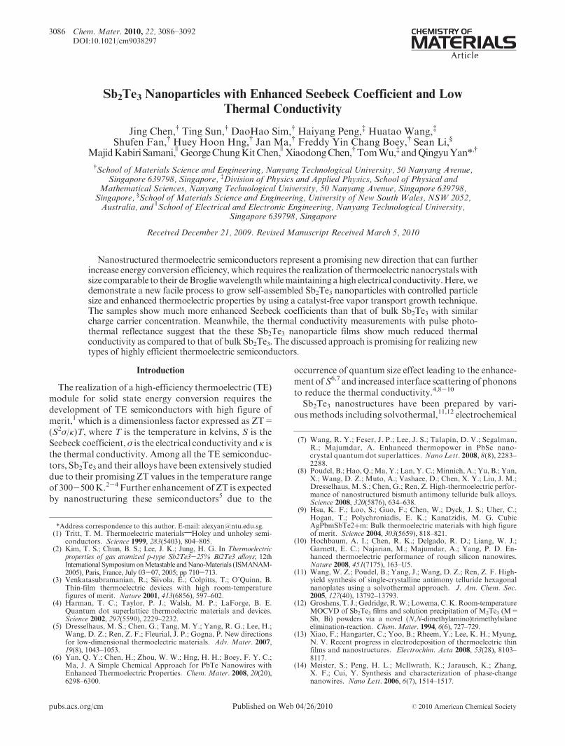
A typical synthesis is carried out by placing two cruci-bles containing Te powder and Sb powder, respectively,in the center of the quartz tube that is heated at 853 Kunder continuous Ar/H2 gas flow to transfer the Sb andTe vapors to be deposited onto glass substrates set in thedownstreampositions. Figure 1 shows the SEM images ofthe as-prepared nanoparticles by the vapor transportgrowth process. Analysis on the SEM images reveals thatthe average particle size of the films is highly dependenton the substrate position/temperature. Films with aver-age particle sizes of 100, 50, and 20 nm were obtained onsubstrates placed at distances of dsub=20, 25, and 30 cmaway from center of the furnace with substrate tempera-tures of 74, 40, and 36 �C, respectively. The substratetemperature is judged from the temperature profile of the
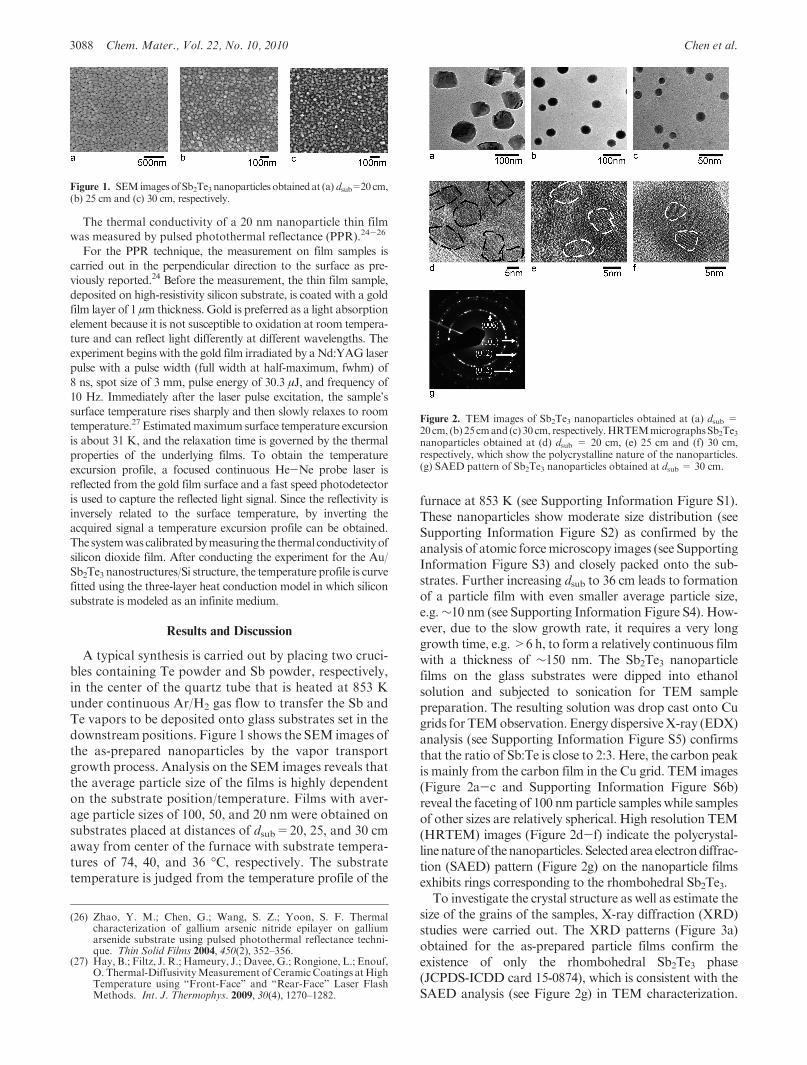
furnace at 853 K (see Supporting Information Figure S1).These nanoparticles show moderate size distribution (seeSupporting Information Figure S2) as confirmed by theanalysis of atomic forcemicroscopy images (see SupportingInformation Figure S3) and closely packed onto the sub-strates. Further increasing dsub to 36 cm leads to formationof a particle film with even smaller average particle size,e.g.∼10 nm (see Supporting Information Figure S4). How-ever, due to the slow growth rate, it requires a very longgrowth time, e.g.>6 h, to form a relatively continuous filmwith a thickness of ∼150 nm. The Sb2Te3 nanoparticlefilms on the glass substrates were dipped into ethanolsolution and subjected to sonication for TEM samplepreparation. The resulting solution was drop cast onto Cugrids forTEMobservation. Energy dispersiveX-ray (EDX)analysis (see Supporting Information Figure S5) confirmsthat the ratio of Sb:Te is close to 2:3. Here, the carbon peakis mainly from the carbon film in the Cu grid. TEM images(Figure 2a-c and Supporting Information Figure S6b)reveal the faceting of 100 nmparticle samples while samplesof other sizes are relatively spherical. High resolution TEM(HRTEM) images (Figure 2d-f) indicate the polycrystal-linenatureof thenanoparticles. Selectedareaelectrondiffrac-tion (SAED) pattern (Figure 2g) on the nanoparticle filmsexhibits rings corresponding to the rhombohedral Sb2Te3.To investigate the crystal structure as well as estimate the
size of the grains of the samples, X-ray diffraction (XRD)studies were carried out. The XRD patterns (Figure 3a)obtained for the as-prepared particle films confirm theexistence of only the rhombohedral Sb2Te3 phase(JCPDS-ICDD card 15-0874), which is consistent with theSAED analysis (see Figure 2g) in TEM characterization.
Figure 1. SEMimages of Sb2Te3 nanoparticles obtainedat (a) dsub=20cm,(b) 25 cm and (c) 30 cm, respectively.
Figure 2. TEM images of Sb2Te3 nanoparticles obtained at (a) dsub =20cm, (b) 25 cmand (c) 30 cm, respectively.HRTEMmicrographsSb2Te3nanoparticles obtained at (d) dsub = 20 cm, (e) 25 cm and (f) 30 cm,respectively, which show the polycrystalline nature of the nanoparticles.(g) SAED pattern of Sb2Te3 nanoparticles obtained at dsub = 30 cm.
(26) Zhao, Y. M.; Chen, G.; Wang, S. Z.; Yoon, S. F. Thermalcharacterization of gallium arsenic nitride epilayer on galliumarsenide substrate using pulsed photothermal reflectance techni-que. Thin Solid Films 2004, 450(2), 352–356.
(27) Hay, B.; Filtz, J. R.; Hameury, J.; Davee, G.; Rongione, L.; Enouf,O. Thermal-DiffusivityMeasurement of CeramicCoatings atHighTemperature using “Front-Face” and “Rear-Face” Laser FlashMethods. Int. J. Thermophys. 2009, 30(4), 1270–1282.
Article Chem. Mater., Vol. 22, No. 10, 2010 3089
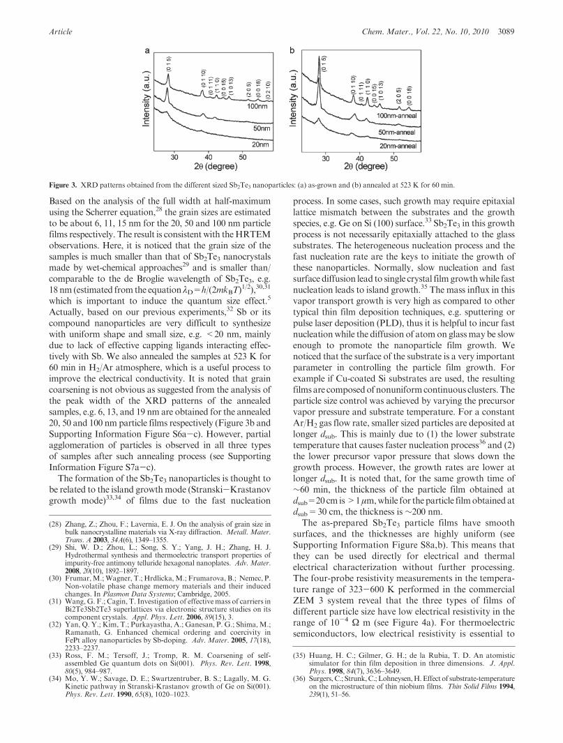
Based on the analysis of the full width at half-maximumusing the Scherrer equation,28 the grain sizes are estimatedto be about 6, 11, 15 nm for the 20, 50 and 100 nm particlefilms respectively. The result is consistent with theHRTEMobservations. Here, it is noticed that the grain size of thesamples is much smaller than that of Sb2Te3 nanocrystalsmade by wet-chemical approaches29 and is smaller than/comparable to the de Broglie wavelength of Sb2Te3, e.g.18 nm (estimated from the equation λD=h/(2mkBT)
1/2),30,31
which is important to induce the quantum size effect.5
Actually, based on our previous experiments,32 Sb or itscompound nanoparticles are very difficult to synthesizewith uniform shape and small size, e.g. <20 nm, mainlydue to lack of effective capping ligands interacting effec-tively with Sb. We also annealed the samples at 523 K for60 min in H2/Ar atmosphere, which is a useful process toimprove the electrical conductivity. It is noted that graincoarsening is not obvious as suggested from the analysis ofthe peak width of the XRD patterns of the annealedsamples, e.g. 6, 13, and 19 nm are obtained for the annealed20, 50 and 100 nm particle films respectively (Figure 3b andSupporting Information Figure S6a-c). However, partialagglomeration of particles is observed in all three typesof samples after such annealing process (see SupportingInformation Figure S7a-c).The formation of the Sb2Te3 nanoparticles is thought to
be related to the island growthmode (Stranski-Krastanovgrowth mode)33,34 of films due to the fast nucleation
process. In some cases, such growth may require epitaxiallattice mismatch between the substrates and the growthspecies, e.g. Ge on Si (100) surface.33 Sb2Te3 in this growthprocess is not necessarily epitaxially attached to the glasssubstrates. The heterogeneous nucleation process and thefast nucleation rate are the keys to initiate the growth ofthese nanoparticles. Normally, slow nucleation and fastsurface diffusion lead to single crystal filmgrowthwhile fastnucleation leads to island growth.35 The mass influx in thisvapor transport growth is very high as compared to othertypical thin film deposition techniques, e.g. sputtering orpulse laser deposition (PLD), thus it is helpful to incur fastnucleationwhile the diffusion of atomon glassmaybe slowenough to promote the nanoparticle film growth. Wenoticed that the surface of the substrate is a very importantparameter in controlling the particle film growth. Forexample if Cu-coated Si substrates are used, the resultingfilmsare composedofnonuniformcontinuous clusters. Theparticle size control was achieved by varying the precursorvapor pressure and substrate temperature. For a constantAr/H2 gas flow rate, smaller sized particles are deposited atlonger dsub. This is mainly due to (1) the lower substratetemperature that causes faster nucleation process36 and (2)the lower precursor vapor pressure that slows down thegrowth process. However, the growth rates are lower atlonger dsub. It is noted that, for the same growth time of∼60 min, the thickness of the particle film obtained atdsub=20 cm is>1μm,while for theparticle filmobtainedatdsub=30 cm, the thickness is ∼200 nm.The as-prepared Sb2Te3 particle films have smooth
surfaces, and the thicknesses are highly uniform (seeSupporting Information Figure S8a,b). This means thatthey can be used directly for electrical and thermalelectrical characterization without further processing.The four-probe resistivity measurements in the tempera-ture range of 323-600 K performed in the commercialZEM 3 system reveal that the three types of films ofdifferent particle size have low electrical resistivity in therange of 10-4 Ω m (see Figure 4a). For thermoelectricsemiconductors, low electrical resistivity is essential to
Figure 3. XRD patterns obtained from the different sized Sb2Te3 nanoparticles: (a) as-grown and (b) annealed at 523 K for 60 min.
(28) Zhang, Z.; Zhou, F.; Lavernia, E. J. On the analysis of grain size inbulk nanocrystalline materials via X-ray diffraction. Metall. Mater.Trans. A 2003, 34A(6), 1349–1355.
(29) Shi, W. D.; Zhou, L.; Song, S. Y.; Yang, J. H.; Zhang, H. J.Hydrothermal synthesis and thermoelectric transport properties ofimpurity-free antimony telluride hexagonal nanoplates. Adv. Mater.2008, 20(10), 1892–1897.
(30) Frumar,M.;Wagner, T.; Hrdlicka,M.; Frumarova, B.; Nemec, P.Non-volatile phase change memory materials and their inducedchanges. In Plasmon Data Systems; Cambridge, 2005.
(31) Wang,G. F.; Cagin, T. Investigation of effectivemass of carriers inBi2Te3Sb2Te3 superlattices via electronic structure studies on itscomponent crystals. Appl. Phys. Lett. 2006, 89(15), 3.
(32) Yan, Q. Y.; Kim, T.; Purkayastha, A.; Ganesan, P. G.; Shima,M.;Ramanath, G. Enhanced chemical ordering and coercivity inFePt alloy nanoparticles by Sb-doping. Adv. Mater. 2005, 17(18),2233–2237.
(33) Ross, F. M.; Tersoff, J.; Tromp, R. M. Coarsening of self-assembled Ge quantum dots on Si(001). Phys. Rev. Lett. 1998,80(5), 984–987.
(34) Mo, Y. W.; Savage, D. E.; Swartzentruber, B. S.; Lagally, M. G.Kinetic pathway in Stranski-Krastanov growth of Ge on Si(001).Phys. Rev. Lett. 1990, 65(8), 1020–1023.
(35) Huang, H. C.; Gilmer, G. H.; de la Rubia, T. D. An atomisticsimulator for thin film deposition in three dimensions. J. Appl.Phys. 1998, 84(7), 3636–3649.
(36) Surgers,C.; Strunk,C.;Lohneysen,H.Effect of substrate-temperatureon the microstructure of thin niobium films. Thin Solid Films 1994,239(1), 51–56.
achieve high ZT values. For all three types of samples, theelectrical resistivity decreases with temperature. Althoughthis trend indicates a typical semiconductor behavior,37
other factorsmay also affect the electrical resistivity of thesesamples, e.g. the annealing effect at higher measuringtemperature leads to partial agglomeration and hence en-hances the contact between the particles, which may alsoincrease the electrical conductance. Thus, the measurementon the annealed samples is used to assess the intrinsic trendof the electrical conductance vs temperature. The enhancedcontact between the particles in the annealed samples isevidenced from the SEM observations (see SupportingInformation Figure S7a-c), and no obvious grain coarsen-ing is observed as indicated by the XRD results (seeFigure 3b). The electrical resistivity of the annealed samplesshows improved values (see Figure 4b) as compared to theircorresponding as-prepared ones. In addition, their valuesincrease at higher temperatures, which is expected in metalsor heavily doped semiconductors.38 Here, we note thatthese electric resistivity values are lower than those of TEnanocrystals obtained by wet chemical process,29 whichis mainly a benefit from clean surface without cappingof insulating ligands. For both the as-prepared and theannealed samples, the lower electrical resistivity shown in
the larger sized particle films is anticipated as the quantumsize effect increases the band gap,7Eg, of the semiconductorparticles.5 The UV absorption spectra (see SupportingInformation Figure S9) reveal that the onset of the thresh-old of absorption curve shows a blue shift for 20 nm Sb2Te3nanoparticles as compared to that of 50 and 100 nmsamples, which suggests the larger band gap value andis consistent with the results of the electrical resistivitymeasurements.The effective charge carrier concentration, n, at room
temperature has been investigated by using a Hall Effectmeasurement system (see Figure 5). For as-prepared sam-ples, the effective charge carrier concentration39 is in therange 3-8� 1019 cm-3, which is ideal to achieve optimizedZT values.40 The effective charge carrier concentrationincreases slightly, e.g. to 6-10� 1019 cm-3, after annealingat 523 K for 60 min for all three types of samples. Thehigher effective charge carrier concentration obtained inlarger sized particle films is expected as increasing the bandgap due to quantum confinementmay decrease the value ofn.7 Based on the charge carrier concentration data, we canestimate the effective hole mobility, μ, of the particle filmsusing σ=neμ (see Supporting Information Figure S10a,b).The estimated effective hole mobility of the samples in-creases by 5-7 times after the heat treatment, which is also
Figure 4. Electrical resistivity of (a) as-grown and (b) annealed Sb2Te3 nanoparticles.
Figure 5. Room-temperature effective charge carrier concentration, n, of (a) as-prepared and (b) annealed Sb2Te3 samples with different particle sizes.
(37) Nagao, Y.; Terasaki, I.; Nakano, T. Dielectric constant and acconductivity of the layered cobalt oxide Bi2Sr2CoO6þdelta: Apossible metal-dielectric composite made by self-organization ofCo2þ and Co3þ ions. Phys. Rev. B 2007, 76 (14).
(38) Brown, S. R.; Toberer, E. S.; Ikeda, T.; Cox, C. A.; Gascoin, F.;Kauzlarich, S. M.; Snyder, G. J. Improved thermoelectric perfor-mance in Yb14Mn1-xZnxSb11 by the reduction of spin-disorderscattering. Chem. Mater. 2008, 20(10), 3412–3419.
(39) Muthukumarasamy, N.; Balasundaraprabhu, R.; Jayakumar, S.;Kannan,M. D. Electrical conduction studies of hot wall depositedCdSexTe1-x thin films. Sol. Energy Mater. Sol. Cells 2008, 92(8),851–856.
(40) Snyder, G. J.; Toberer, E. S. Complex thermoelectric materials.Nat. Mater. 2008, 7(2), 105–114.
Article Chem. Mater., Vol. 22, No. 10, 2010 3091
in line with the increased electrical conductance. Thissuggests that enhanced contact among the particles afterannealing can effectively reduce the interface scattering ofthe charge carriers.Thermoelectric characterization with the ZEM 3 system
shows that all three sized Sb2Te3 particle films are p-typewith high maximum Seebeck coefficients, e.g.>200 μV/K,>180μV/K,and>160μV/K for 20 nm, 50nmand100nmparticle films, respectively (see Figure 6a). These values arehigher than that of bulk Sb2Te3 crystals (79 μV/K) withsimilar charge carrier concentrations20,21 and that ofSb2Te3 thin film.41 If the Sb2Te3 nanocrystal size isincreased by decreasing the dsub, the Seebeck coefficient isreduced to 60-95 μV/K in the same temperature range (seeSupporting Information Figure S11) while the Sb2Te3 aresingle-crystal nanoplates with a diameter of 2-3 μm and athickness of 80-200nm.The enhancedSeebeck coefficient,S, in smaller particles is thought to be possibly related to thequantum confinement effect that increases the differencebetween the Fermi level and the average mobile carrierenergy,7 or to be related to the energy filtering effect due tothe charge carrier trapped in the grainboundaries regions.42
All three sized particle films show increased S at highertemperature range. For heavily doped semiconductor ormetal, the electron contribution to S is proportional to the
absolute temperature.43 The values of S for the annealedsamples are comparable to those of the as-prepared ones(see Figure 6b), although their electrical resistivities aresignificantly lower.The plots of power factor (see Figure 7) defined asS2σ of
the as-prepared samples show values>3� 10-4W/mK2 atT>550K. The power factors for the annealed samples aresignificantly improved by 2-3 times. A maximum powerfactor >1.1 � 10-3 W/mK2 was measured in the 20 nmparticle films at T=500 K. The smaller sized particle filmsshowhigher power factormainly due to the contribution oftheir higher values of Seebeck coefficients.The measurement of κ for nanostructures or even thin
films is very difficult10,44 due to the small feature size.Here, we carried out the pulsed photothermal reflectance(PPR)24,25 process to evaluate the thermal conductivity ofthe samples. Here, we noted that the PPR measurementscan only test the thermal conductivity along the normalof the particle film surface while the previous discussionon the Seebeck and electrical conductivity is along thesurface of the samples. Although these nanoparticle-assembled films are expected to be isotropic because oftheir unique build-up structures, we cannot claim ZTvalues based on these measurements. For the PPR meth-od as discussed in detail in the Experimental Section (alsosee Supporting Information Figure S12), the thermalconductivity, κ, is obtained by curve fitting the timedependence surface temperature profile of the Au filmcoated samplewith the three-layer heat conductionmodel
Figure 6. Seebeck coefficients of (a) as-grown and (b) annealed Sb2Te3 nanoparticles.
Figure 7. Power factors of (a) as-grown and (b) annealed Sb2Te3 nanoparticles.
(41) Rajasekar, K.; Kungumadevi, L.; Subbarayan, A.; Sathyamoorthy,R. Thermal sensors based on Sb2Te3 and (Sb2Te3)(70)(Bi2Te3)(30)thin films. Ionics 2008, 14(1), 69–72.
(42) Martin, J.; Wang, L.; Chen, L.; Nolas, G. S. Enhanced Seebeckcoefficient through energy-barrier scattering in PbTe nanocompo-sites. Phys. Rev. B 2009, 79(11), 5.
(43) Rowe,D.M.CRChandbook of thermoelectrics; CRCPress: London,New York, Washington, DC, 1995.
(44) Boukai,A. I.; Bunimovich,Y.; Tahir-Kheli, J.; Yu, J.K.;Goddard,W. A.; Heath, J. R. Silicon nanowires as efficient thermoelectricmaterials. Nature 2008, 451, 168–171.
(see Supporting Information Figure S13a-f). Althoughthe PPRmeasurements have the advantages that they donotrequire the known values of density and specific heat of thesamples, only room-temperature thermal conductivity of as-prepared and annealed samples can be obtained (see Table 1andSupporting InformationFigure S13a-f) due to the limitof instrumental setup. The PPRmeasurement indicates thatthe 20 nm Sb2Te3 nanoparticle films show much reducedvalues of κ at room temperature, e.g. 0.23 W/mK for as-prepared samples and 0.33 W/mK for annealed samples,which is much lower than that reported for compact bulkSb2Te3, e.g. ∼1 W/mK.45 The values of the thermal con-ductivity for Sb2Te3 samples with different particles sizes,e.g. 0.2-0.5 W/mK for as-prepared particles and 0.3-0.8 W/mK for annealed particles, are comparable to thoserecently reported values for Bi2Te3 nanoparticles.
46,47 Here,the estimated carrier thermal conductivity is not high,
e.g 0.012-0.04 W/mK for as-prepared samples and0.17-0.26W/mK for annealed samples, usingWiedemann-Franz’s law,48,49 e.g. κcarrier=LT/F, where L is the Lorenznumber, e.g. 2.45� 10-8V2K-2,F is the electrical resistivity,and T is the temperature in kelvins. Preparation of theseSb2Te3 nanoparticles in large scale can further enable accu-rate thermal conductivity measurements by laser flashprocess27 to enable estimation of the ZT values, which isongoing now.Also, further enhanced thermoelectric proper-ties can be expected by applying this approach to preparenanoparticles of other material systems with proven higherZT values, e.g. BiSbTe4,8 or AgPbSbTe.9
In summary, we have demonstrated a new facile pro-cess to grow Sb2Te3 nanoparticle films with controlledparticle size using a catalyst-free vapor transport growthtechnique. Such a growth process allows the realization ofnanocrystal films with tunable crystal size, e.g. 5-15 nm,comparable to the de Broglie wavelength of Sb2Te3. Theenhancement of the Seebeck coefficients has been demon-strated in these nanoparticle films as compared to that ofbulk Sb2Te3 with similar charge carrier concentration.Meanwhile, these particle films show high electrical con-ductivities due to the clean particle surfaces. The PPRmeasurements at room temperature suggest that thesenanoparticle films show much reduced thermal conduc-tivity as compared to that of bulk Sb2Te3. Thus, thisapproach demonstrates a promising route to achieve newtypes of highly efficient TE semiconductors.
Acknowledgment. The authors gratefully acknowledgethe AcRF Tier 1 RG 31/08 from MOE, Singapore andthe DSO National Laboratories funding (Project agreementnumber: DSOCL09015).
Supporting Information Available: Temperature profile of
the furnace, morphology and the estimated mobility of the
samples, detail of PPR measurement (PDF). This material is
available free of charge via the Internet at http://pubs.acs.org.
Table 1. Room Temperature Thermal Conductivity (W/mK) of Sb2Te3Nanoparticle Samples Determined by Pulsed Photothermal Reflectance
as-prepared samples annealed samples
100 nm 50 nm 20 nm 100 nm 50 nm 20 nm
0.5 0.38 0.23 0.78 0.55 0.33
(45) Wang, W.; Yan, X.; Poudel, B.; Ma, Y.; Hao, Q.; Yang, J.; Chen,G.; Ren, Z. Chemical synthesis of anisotropic nanocrystallineSb2Te3 and low thermal conductivity of the compacted densebulk. J. Nanosci. Nanotechnol. 2008, 8(1), 452–456.
(46) Scheele, M.; Oeschler, N.; Meier, K.; Kornowski, A.; Klinke, C.;Weller, H. Synthesis and Thermoelectric Characterization ofBi2Te3 Nanoparticles. Adv. Funct. Mater. 2009, 19(21), 3476–3483.
(47) Dirmyer, M. R.; Martin, J.; Nolas, G. S.; Sen, A.; Badding, J. V.Thermal and Electrical Conductivity of Size-Tuned Bismuth Tell-uride Nanoparticles. Small 2009, 5(8), 933–937.
(48) Yang, L.; Hng, H. H.; Li, D.; Yan, Q. Y.; Ma, J.; Zhu, T. J.; Zhao,X. B.; Huang, H., Thermoelectric properties of p-type CoSb3nanocomposites with dispersed CoSb3 nanoparticles. J. Appl.Phys. 2009, 106, (1).
(49) Li, D.; Yang, K.; Hng, H. H.; Yan, Q. Y.; Ma, J.; Zhu, T. J.; Zhao,X. B., Synthesis and high temperature thermoelectric properties ofcalcium and cerium double-filled skutterudites Ca0.1CexCo4Sb12.J. Phys. D: Appl. Phys. 2009, 42 (10).


![Polymer gels with tunable ionic Seebeck coefficient for ...liu.diva-portal.org/smash/get/diva2:1294209/FULLTEXT01.pdfpolymer gel composed of [EMIM][TFSI] and the PVDF-HFP matrix is](https://static.documents.pub/doc/80x56/5fa1f1b9ef36275d2e6ad3bd/polymer-gels-with-tunable-ionic-seebeck-coefficient-for-liudiva-1294209fulltext01pdf.jpg)


![Influence of Doping Concentration and Ambient Temperature ... · successfully measured the Seebeck coefficient by integrating a thin film heater on top of the microcooler [21]. In](https://static.documents.pub/doc/80x56/5e7630d6882a7c19c30f6d30/influence-of-doping-concentration-and-ambient-temperature-successfully-measured.jpg)


