Life Science Journal 2012;9(3) http://www.lifesciencesite.com 1646 A Novel Nanometric Reversible Four-bit Signed-magnitude Adder/Subtractor Soudebeh Boroumand Department of Computer Engineering, Tabriz Branch, Islamic Azad University, Tabriz, Iran [email protected]Abstract: The reversible logic plays a significant role in the synthesis of circuits for quantum computing. Reversible gates have been widely used in low power CMOS design, optical information processing, and bioinformatics, quantum computing and nanotechnology-based systems. A new 3×3 reversible two’s complement gate is suggested in this paper. Two quantum models are offered for two’s complement gate. These quantum models differ from each other with respect to the quantum cost. Two novel reversible four-bit signed-magnitude adders/subtractors with HNG and ADD/SUB gates are also proposed for the first time. The proposed circuits detect overflow and produce a correct result for inputs in the range of [-7, 7]. The proposed two’s complement gate is used in part of the reversible four-bit signed-magnitude adder/subtractor design. The proposed reversible 4-bit signed-magnitude adders/subtractors are evaluated in terms of number of reversible gates, number of garbage outputs, number of constant inputs, quantum cost and hardware complexity. All the scales are in the nanometric area. [Boroumand S. A Novel Nanometric Reversible Four-bit Signed-magnitude Adder/Subtractor. Life Sci J 2012;9(3):1646-1655]. (ISSN: 1097-8135). http://www.lifesciencesite.com . 240 Key words: nanotechnology based systems; quantum computing; reversible logic; reversible signed-magnitude adder/subtractor. 1. Introduction One of the most prominent incentives for the study of reversible computing comes from the desire to reduce heat dissipation in computing machinery, and thus achieve higher density and speed (Toffoli, 1980). Reversible computing, in a general sense, means computing using reversible operations, that is, operations that can be easily and exactly reversed, or undone. Reversible operations realize bijective Boolean functions. Conventional gates such as AND, XOR, OR, etc., that are used in digital design are not reversible. Landauer (1961) proved that classical non-reversible circuits inevitably produce heat because of losses of information during the computation. Landauer’s principle (Landauer, 1961) states that generated heat for each bit of information lost is KTln2 joules of energy, Where K= 1.3806505*10 -23 m 2 kg -2 K -1 (joule/Kelvin) is Boltzmann constant and T is the temperature in Kelvin degrees at which operation is performed. Bennett’s (Bennett, 1973) theory was developed to compensate energy dissipation. Bennett’s theorem suggests that every future binary technology will have to use some kind of reversible gates in order to reduce heat dissipation (Mozammel, 2008). Bennett (Bennett, 1973) showed that zero energy dissipation is possible in Reversible logic computing, that is a reversible logic gate has a one-to-one mapping between the inputs and outputs. Some restrictions of reversible circuits include Fan-out and loop or feedback. Recently, researchers illustrated that feedback is allowed in reversible computing in a case of sequential circuit's design (Thapliyal and Ranganathan, 2010). Quantum technology is inherently reversible and it will become very important for future computing systems (Mozammel, 2008). In reversible logic the output logical states uniquely define the input logical states of the computational operation. Reversible logic circuits encompass the same number of input and output lines. Such circuits (gates) can produce inputs from the corresponding outputs and vice versa. On the other hand, the digital computer is a digital system that performs various computational tasks by arithmetic circuits such as Adders, Subtractors, Multipliers and Dividers from which Adders and Subtractors are the most essential blocks of a computing system. So some reversible Adders and Subtractors for unsigned numbers have been proposed in (6-14) and only one paper (Emam and Elsayed, 2010) has been proposed so far on reversible Adder/Subtractor for signed/unsigned binary numbers. The author in (Emam and Elsayed, 2010) proposed a circuit for addition and subtraction signed numbers represented in two’s complement representation and no circuit for addition and subtraction signed numbers represented in the signed- magnitude representation so far, has been designed. For floating-point operations, most computers use the signed-magnitude representation for the mantissa, so addition and Subtraction floating-point numbers needed signed-magnitude Adder/Subtractor. Thus, in this article a circuit is proposed for Addition and Subtraction signed numbers represented in the signed-magnitude representation.
Transcript
Life Science Journal 2012;9(3) http://www.lifesciencesite.com
1646
A Novel Nanometric Reversible Four-bit Signed-magnitude Adder/Subtractor
Soudebeh Boroumand
Department of Computer Engineering, Tabriz Branch, Islamic Azad University, Tabriz, Iran [email protected]
Abstract: The reversible logic plays a significant role in the synthesis of circuits for quantum computing. Reversible gates have been widely used in low power CMOS design, optical information processing, and bioinformatics, quantum computing and nanotechnology-based systems. A new 3×3 reversible two’s complement gate is suggested in this paper. Two quantum models are offered for two’s complement gate. These quantum models differ from each other with respect to the quantum cost. Two novel reversible four-bit signed-magnitude adders/subtractors with HNG and ADD/SUB gates are also proposed for the first time. The proposed circuits detect overflow and produce a correct result for inputs in the range of [-7, 7]. The proposed two’s complement gate is used in part of the reversible four-bit signed-magnitude adder/subtractor design. The proposed reversible 4-bit signed-magnitude adders/subtractors are evaluated in terms of number of reversible gates, number of garbage outputs, number of constant inputs, quantum cost and hardware complexity. All the scales are in the nanometric area. [Boroumand S. A Novel Nanometric Reversible Four-bit Signed-magnitude Adder/Subtractor. Life Sci J 2012;9(3):1646-1655]. (ISSN: 1097-8135). http://www.lifesciencesite.com. 240 Key words: nanotechnology based systems; quantum computing; reversible logic; reversible signed-magnitude adder/subtractor. 1. Introduction
One of the most prominent incentives for the study of reversible computing comes from the desire to reduce heat dissipation in computing machinery, and thus achieve higher density and speed (Toffoli, 1980). Reversible computing, in a general sense, means computing using reversible operations, that is, operations that can be easily and exactly reversed, or undone. Reversible operations realize bijective Boolean functions. Conventional gates such as AND, XOR, OR, etc., that are used in digital design are not reversible. Landauer (1961) proved that classical non-reversible circuits inevitably produce heat because of losses of information during the computation. Landauer’s principle (Landauer, 1961) states that generated heat for each bit of information lost is KTln2 joules of energy, Where K= 1.3806505*10-23m2 kg-2 K-1 (joule/Kelvin) is Boltzmann constant and T is the temperature in Kelvin degrees at which operation is performed. Bennett’s (Bennett, 1973) theory was developed to compensate energy dissipation. Bennett’s theorem suggests that every future binary technology will have to use some kind of reversible gates in order to reduce heat dissipation (Mozammel, 2008). Bennett (Bennett, 1973) showed that zero energy dissipation is possible in Reversible logic computing, that is a reversible logic gate has a one-to-one mapping between the inputs and outputs. Some restrictions of reversible circuits include Fan-out and loop or feedback. Recently, researchers illustrated that feedback is allowed in reversible computing in a case of sequential circuit's design (Thapliyal and
Ranganathan, 2010). Quantum technology is inherently reversible and it will become very important for future computing systems (Mozammel, 2008). In reversible logic the output logical states uniquely define the input logical states of the computational operation. Reversible logic circuits encompass the same number of input and output lines. Such circuits (gates) can produce inputs from the corresponding outputs and vice versa. On the other hand, the digital computer is a digital system that performs various computational tasks by arithmetic circuits such as Adders, Subtractors, Multipliers and Dividers from which Adders and Subtractors are the most essential blocks of a computing system. So some reversible Adders and Subtractors for unsigned numbers have been proposed in (6-14) and only one paper (Emam and Elsayed, 2010) has been proposed so far on reversible Adder/Subtractor for signed/unsigned binary numbers. The author in (Emam and Elsayed, 2010) proposed a circuit for addition and subtraction signed numbers represented in two’s complement representation and no circuit for addition and subtraction signed numbers represented in the signed-magnitude representation so far, has been designed. For floating-point operations, most computers use the signed-magnitude representation for the mantissa, so addition and Subtraction floating-point numbers needed signed-magnitude Adder/Subtractor. Thus, in this article a circuit is proposed for Addition and Subtraction signed numbers represented in the signed-magnitude representation.
Life Science Journal 2012;9(3) http://www.lifesciencesite.com
1647
The paper is structured around the following sections: section 2 discusses the proposed reversible gate and some necessary reversible logic gates. Section 3 provides essential background on irreversible signed-magnitude full adder/subtractor. The proposed four-bit reversible signed-magnitude adders/subtractors with HNG and ADD/SUB gates and different parts of the proposed reversible signed-magnitude Adder/Subtractor are described in section 3 too. The simulation results with VHDL language and Quartus simulator is shown in section 4 and conclusions are contained in section 5. 2. Reversible Gates
The quantum cost(QC) of any reversible gate(circuit) is the number of 1×1 or 2×2 reversible gates and quantum logic gates such as V, V+ (V is
also named square root of NOT gate NOT and V+
is hermitian of V). The V and V+ quantum gates have some properties that are shown in Equation (1) (Mohammadi et al., 2009).
(1)
NOTVV
IVVVV
NOTVV
Any reversible logic gate (circuit) is realized by using mentioned gates above, NOT and FG gates. This section proposes a new reversible logic gate which is termed two’s complement gate as shown in Figure 1, and its truth table is presented in Table 1. Then this section introduces NLG and ADD/SUB gates. For aware of other utilized reversible gates such as NOT, FG, F2G, FRG, HNFG, HNG, PG you can refer to (13-19) references. Two’s complement Gate
A new 3×3 reversible logic gate is 2’s complement gate. This gate is very important in circuits design because Complements are used in digital computers for logical operation and simplifying the subtraction function. The proposed reversible 2’s complement gate is depicted in Figure 1. The 2’s complement gate can be represented as:
),,(
),,(
ABCBARBAQAPO
CBAI
v
v
Where, IV and OV are the input and output vectors.
A
B
C
P=A
Two’s Complement
Gate
BAQ
ABCBAR Figure 1. The proposed Two’s Complement Gate
Figure 2. Characteristics of a self-inverse gate
Reversible 2’s complement gate is a one through gate, and its truth table is shown in table 1. According to this table for every input pattern there is a unique output pattern. Reversible 2’s complement gate is also a self-inverse gate. A function is self-inverse, If an input x into the function ƒ produces an
output y, then putting y into the inverse function 1f
produces the output x, and vice versa. Figure 2 shows the characteristics of a self-inverse gate.
Table 1. Truth table of 2’s complement gate
Two quantum models are proposed for this
gate which is demonstrated in Figure 3. The quantum cost of reversible 2’s complement gate is 6 in Figure 3a. The QC is 5, in Figure 3b. The optimized QC is 5 for this gate.
(a) (b)
Figure 3. Two quantum models for Two’s Complement Gate
C B A R Q P
0 0 0 0 0 0
0 0 1 1 1 1
0 1 0 1 1 0 0 1 1 1 0 1
1 0 0 1 0 0
1 0 1 0 1 1 1 1 0 0 1 0
1 1 1 0 0 1
Life Science Journal 2012;9(3) http://www.lifesciencesite.com
1648
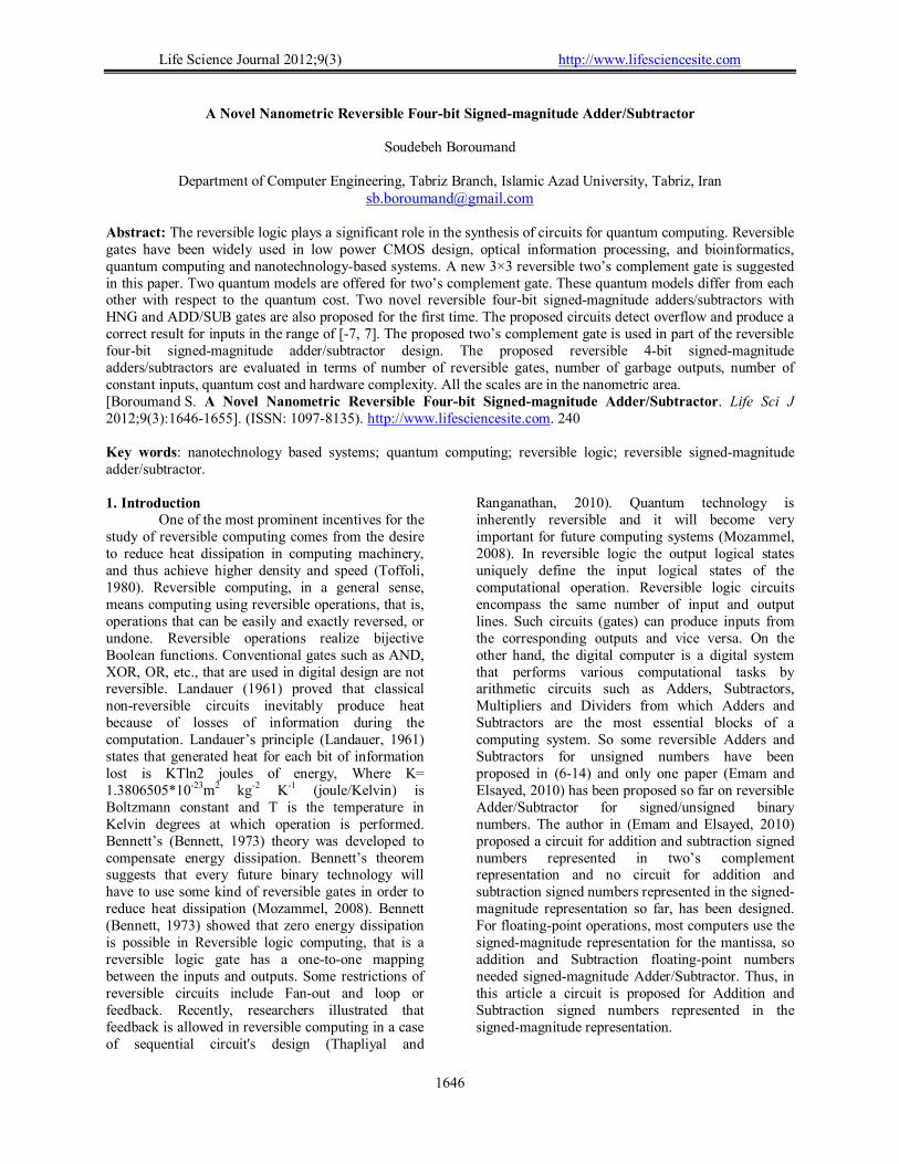
NLG Gate NLG gate is abbreviation for new reversible
logic gate that has been proposed in (Lihui et al., 2010) for the first time. NLG gate is a one through gate as shown in figure 4. Quantum model and Quantum cost of this gate has not been reported in
(Lihui et al., 2010). So this article proposes two quantum models for this gate which are demonstrated in figure 5. Figure 5a uses quantum gates V and V+ and Figure 5b uses FG and NOT gate. The quantum cost is four in Figure 5a and it is one in Figure 5b which is the lowest quantum cost.
ABBAQ
Figure 4. NLG gate
(a) (b)
Figure 5. Proposed equivalent quantum representation of NLG gate
ADD/SUB Gate
ADD/SUB gate is a reversible 4×4 gate. It has been proposed in (Emam and Elsayed, 2010) for the first time. This gate can be represented as:
),,/,(
),,,(
BFSARBCQCBAPO
CBAFI
v
v
Where IV and OV are the input and output vectors. If F input is set to zero then the ADD/SUB gate will work as a reversible full adder or else the gate will work as a reversible full subtractor as shown in figures 6b and 6c respectively.
CBAS/D
C/B
BF
CBAS
BCACABC
B
BCCABAB
CBAD
(a) (b) (c)
Figure 6. Reversible ADD/SUB gate (a) symbol, (b) Full Adder, (c) Full Subtractor 3. Basic Concepts
There are two different common forms of representation for negative fixed-point numbers in a radix r system.
1. Sign and magnitude representation, which is also called the signed-magnitude method.
2. Complement representation which comprises two alternatives: (I) Two’s complement in the binary system
(II) One’s complement in the binary system When an integer binary number is positive,
the sign is represented by 0 and the magnitude by a positive binary number. When the number is negative, the sign is represented by 1 but the rest of the number may be represented in one of the three aforementioned ways (signed-magnitude, one’s complement and two’s complement representation).
Reversible Signed numbers Adder/Subtractor circuit design based on these methods will be different. In this article the main opinion is designing reversible signed-magnitude adder/subtractor. The algorithm for signed-magnitude adder/subtractor is more complex than addition and subtraction numbers in signed-complement system, because not only it needs circuits to add and subtract but also its implementation needs circuits to compare the signs and the magnitudes of the numbers. The range of n bit integer numbers in the signed-magnitude system is symmetric and equals
)12()12( 11 nn X
So the range of 4 bits integer numbers in the signed-magnitude system is [-7, 7]. The leftmost bit of the signed-magnitude number shows the number sign. As a result, there are two representations of
Life Science Journal 2012;9(3) http://www.lifesciencesite.com
1649
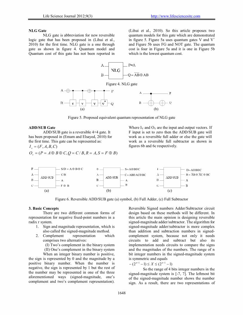
zero, a positive zero represented by 000...0, and a negative zero represented by 100...0, but in addition and subtraction for signed-magnitude numbers only positive zero is produced, so this is one advantages of the proposed design. The signed-magnitude adder/subtractor flowchart is presented in figure 7. A, B determine the magnitude of the two numbers and As, Bs show the signs of A and B respectively. According to the flowchart, As and Bs determine
addition or subtraction operation. If 0 sBsA then
the signs will be identical otherwise the signs will be different. Depending on the selected operation, adding or subtracting, the micro operations
BAES or BAES is done (subtraction with two’s complement method). E indicates the output carry when A and B are added. An overflow may occur if the two numbers added are both positive and both negative. So if the carry in E is equal to one then the overflow will occur. Since the addition and subtraction of the four bit signed-magnitude numbers are covered in the range of [-7, 7], the final result is considered 5 bits (because of the overflow). According to the existence flowchart in figure 7, If
the micro operation 1 BAES is done and E is equal to one (E=1) then A will be larger than or equal to B (A≥B). In this case if S=0 then A will equal to B and the sign Ss must be positive to avoid a negative zero, otherwise A will be larger than B (A>B) and the number in S is the correct result. If E is equal to zero (E=0) then A will be less than B (A<B), thus the sign Ss is equivalent to complement the sign of A and the correct result is the two’s complement of the value in S (Koren, 1945; Mano, 2001).
3.1 Proposed Design
Figure 8 shows the traditional block diagram of the proposed design. This block Adds/Subtracts two signed-magnitude four bit numbers. It has nine inputs consisting of A and B inputs that each are three bits and two signed bits AS and BS, and CF/S signal is also used as the control input. If CF/S = 0, the operands are added otherwise they are subtracted. This block diagram has also four outputs consisting of SS which is considered as a signed bit for output bits and E, S0, S1 and S2 outputs. Since the addition and subtraction of the four bit signed-magnitude numbers are covered in the range of [-7, 7], the final result is considered 5 bits. This article based on this block diagram and aforesaid flowchart in previous section proposes a Four-bit Reversible Signed-magnitude Full Adder/Subtractor. Therefore in next
sections, necessary parts are introduced for designing this circuit. 3.2 The proposed Circuit for Input Ctrl Signal of Reversible Ripple Adder/Subtractor with HNG gate
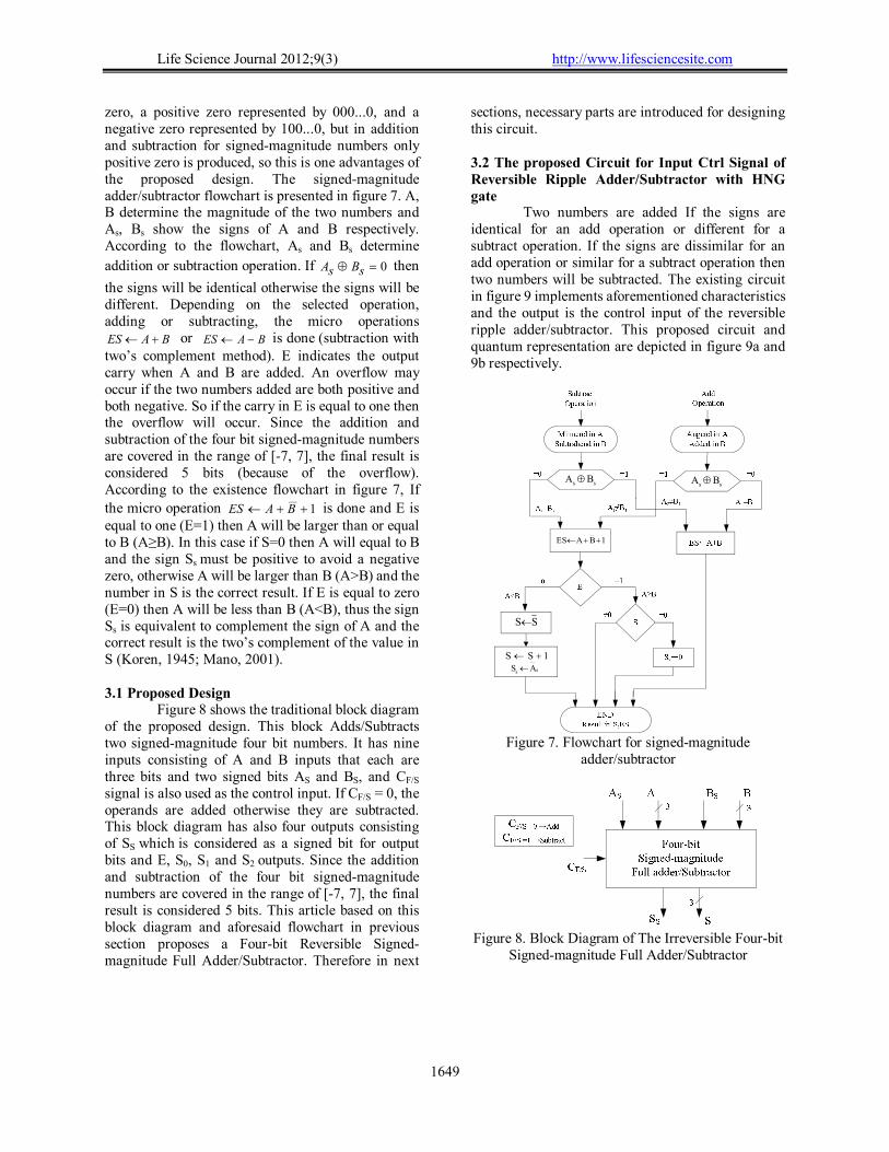
Two numbers are added If the signs are identical for an add operation or different for a subtract operation. If the signs are dissimilar for an add operation or similar for a subtract operation then two numbers will be subtracted. The existing circuit in figure 9 implements aforementioned characteristics and the output is the control input of the reversible ripple adder/subtractor. This proposed circuit and quantum representation are depicted in figure 9a and 9b respectively.
ss BA ss BA
1BAES
SS
ss AS
1SS
Figure 7. Flowchart for signed-magnitude
adder/subtractor
Figure 8. Block Diagram of The Irreversible Four-bit
Signed-magnitude Full Adder/Subtractor
Life Science Journal 2012;9(3) http://www.lifesciencesite.com
1650
Subtract1
Add0C F/S
(a) (b)
Figure 9. Two symbols of Proposed Circuit For Control Input
The existence circuit in figure 9 has three
outputs consist of two garbage outputs and Ctrl output that is connected to control input of the reversible ripple adder/subtractor. If Ctrl= 0, the operands are
added otherwise they are subtracted (two’s
complement method). Reversible Four-bit Signed-
magnitude Adder/Subtractor design requires a three-bit reversible two’s complement adder/subtractor. The reversible two’s complement adder/subtractor with proposed circuit for Ctrl signal and its quantum implementation are shown in figure 10 and 11 respectively.
Subtract1
Add0C F/S
Figure 10. The reversible adder/subtractor with proposed Ctrl signal
As can be seen in figure 10 if Ctrl=0, then
the micro operation BAS will be performed
otherwise the micro operation 1 BAS will be performed. The existing design in figure 10 has 9
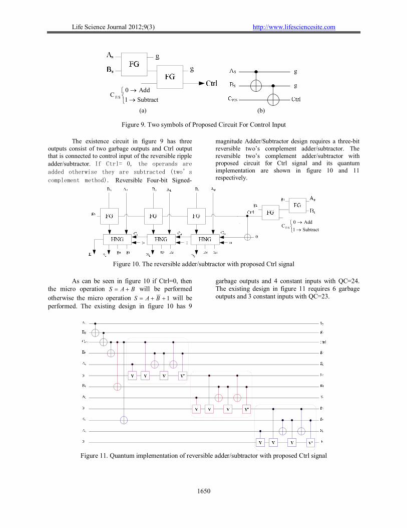
garbage outputs and 4 constant inputs with QC=24. The existing design in figure 11 requires 6 garbage outputs and 3 constant inputs with QC=23.
Figure 11. Quantum implementation of reversible adder/subtractor with proposed Ctrl signal
Life Science Journal 2012;9(3) http://www.lifesciencesite.com
1651
3.3 Proposed Circuit for A=B State If Ctrl signal is set to one then micro
operation 1 BAES will be done. In this case if E is equal to one and the number in S is equal to zero then A will be equal to B. Therefore in this section a reversible circuit is proposed to compare the existing number in S with zero. Thus, when A is equal to B, the number in S is the correct result, but the sign Ss
must be positive to avoid a negative zero. For implementation circuit that compares the result with zero, we can use the following equation: (2)
The proposed circuit Based on the equation (2) is demonstrated in figure 12. This proposed circuit have been designed using NLG and PG gates with QC=11. It needs 5 constant inputs, 7 garbage outputs and 5 gates. DC inputs and outputs are an important figure of merit to evaluate a design. In this research, the quantum model is proposed to optimize garbage inputs and outputs. As it is shown in figure 12b, the quantum circuit has 2 DC inputs, and 4 DC outputs and 5 gates. The quantum cost of the circuit is also 11.
(a) (b)
Figure 12. The reversible circuit for comparing the 3 bit number with zero
3.4 investigating Circuit In A>B State
If Ctrl signal is set to one then micro
operation 1 BAES will be done. In this case if E is equal to one and the number in S is opposite of zero then A will be larger than B. Therefore the number in S is the correct result and the sign of the result is the same as the sign of A, so no change in AS is required. Thus it is required to use multiplexer 2×1 in order to select the sign of SS between two states A=B and A>B. Fredkin gate is applied as a multiplexer in figure 13. Note that this reversible multiplexer has 3 inputs (0, AS and control) and one main output and 2 garbage outputs. F (A=B) signal in figure 12 is used as the control input for multiplexer. The reversible multiplexer applies 0 for A=B(S=0) state or AS for A>B (S≠0) state.
Figure 13. FRG as a MUX 2×1 for implementation
sign bit 3.5 investigating Circuit In A<B State
If the 1 BAES operation is performed and E is equal to zero then A will be less than B. In this case the two’s complement of the value in S must be obtained to create the correct result. In the proposed circuit this operation is done
by using Two’s complement gate. In this case the sign of result is the complement of the original sign of A, so AS is complemented by using NOT gate for obtaining the correct sign. 3.6 Proposed Four-bit Reversible Signed-magnitude Adder/Subtractor with HNG gate
Four-bit reversible signed-magnitude adder/subtrator is proposed in figure 14. The circuit function is described, according to the existing flowchart in Figure 7 and table 2.
Table 2. Determining operations and carry out in Adder/Subtractor
ctrl E 0 0 0 1 1 0 1 1
The proposed design utilizes two FRG gates
(F1&F2) as a multiplexer 4×1 to determine the sign S and also four FRG gates (F3, F4, F5 & F6) to distinguish the final result (ES). In the first and second rows of Table 2, the Ctrl signal is zero and AS passes to the second output of FRG (F2) gate (SS), and when the Ctrl signal is set to one in the next rows, depending on the value of E, signal sA or
sS
passes to the second output of FRG (F2) gate (SS).
Life Science Journal 2012;9(3) http://www.lifesciencesite.com
1652
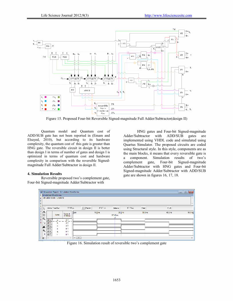
Figure 14. Proposed Four-bit Reversible Signed-magnitude Full Adder/Subtractor(design I)
In proposed Four-bit Reversible Signed-
magnitude Full Adder/Subtractor, when Ctrl=0 overflow may occur, therefore because of this overflow, FRG gate (F3) is considered. It means that F3 is used for detecting overflow and obtaining the correct result for inputs in the range of [-7, 7]. K input is a control signal for three FRG gates (F4, F5 & F6) which are located in the right side and down position of the proposed circuit. If the K input is zero then the result (S2S1S0) is equal to the number in S; otherwise, it is Two’s complement of the value in S. logical equation (3) can be written for control K signal.
(3) ECtrlK According to the equation 3, K is only one in 10 state of the Table 3 and it is zero in rest of states. 3.7 Proposed Four-bit Reversible Signed-magnitude Adder/Subtractor with ADD/SUB Gate
This circuit(design II) has been implemented with ADD/SUB gates instead of HNG gates, so
subtraction operation is not performed using two’s complement method. The borrow output of this design is different from previous design. In this circuit if E is equal to one then A will be less than B otherwise A will be larger than or equal to B therefore the K control input is changed and obtained from equation (4).
(4) )( ECtrlK
On the other hand, inputs of F1 in previous
design is swapped, it means that in Ctrl E=10 state the
sS signal and Ctrl E=11 state sA signal stand in
final sign bit. Proposed Four-bit Reversible Signed-magnitude Adder/Subtractor with ADD/SUB Gates is shown in figure 15. A comparison between the two circuits for the Reversible Signed-magnitude Full Adder/Subtractor is shown in table 3.
Table 3. Comparison between Design I and design II
Total Logical Calculation Quantum Cost NO. of Garbage
outputs NO. of Constant
inputs NO. of gates
84 21 17 26 Design I Figure 14
65+3(QC(ADD/SUB)) 21 17 23
Design II Figure 15
Life Science Journal 2012;9(3) http://www.lifesciencesite.com
1653
Figure 15. Proposed Four-bit Reversible Signed-magnitude Full Adder/Subtractor(design II)
Quantum model and Quantum cost of
ADD/SUB gate has not been reported in (Emam and Elsayed, 2010), but according to its hardware complexity, the quantum cost of this gate is greater than HNG gate. The reversible circuit in design II is better than design I in terms of number of gates and design I is optimized in terms of quantum cost and hardware complexity in comparison with the reversible Signed-magnitude Full Adder/Subtractor in design II.
4. Simulation Results
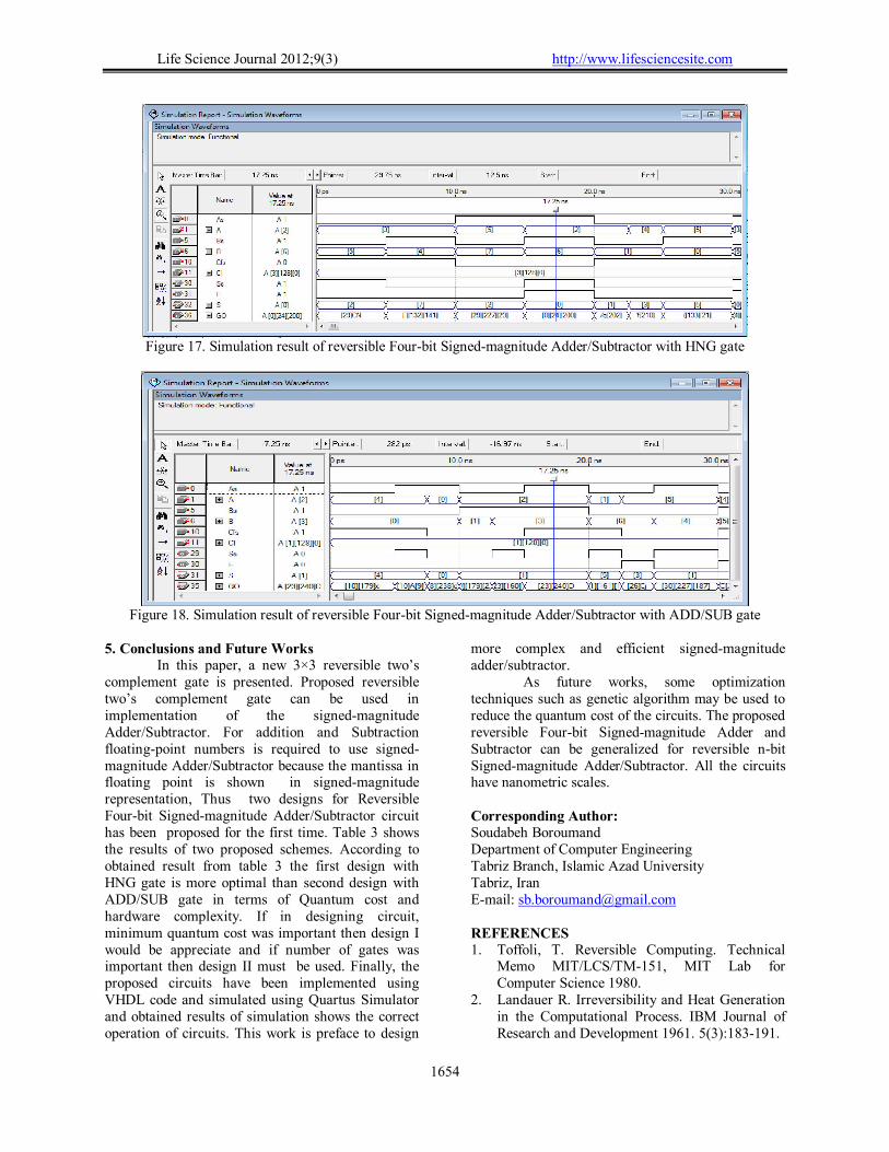
Reversible proposed two’s complement gate, Four-bit Signed-magnitude Adder/Subtractor with
HNG gates and Four-bit Signed-magnitude Adder/Subtractor with ADD/SUB gates are implemented using VHDL code and simulated using Quartus Simulator. The proposed circuits are coded using Structural style. In this style, components are as the main blocks, it means that every reversible gate is a component. Simulation results of two’s complement gate, Four-bit Signed-magnitude Adder/Subtractor with HNG gates and Four-bit Signed-magnitude Adder/Subtractor with ADD/SUB gate are shown in figures 16, 17, 18.
Figure 16. Simulation result of reversible two’s complement gate
Life Science Journal 2012;9(3) http://www.lifesciencesite.com
1654
Figure 17. Simulation result of reversible Four-bit Signed-magnitude Adder/Subtractor with HNG gate
Figure 18. Simulation result of reversible Four-bit Signed-magnitude Adder/Subtractor with ADD/SUB gate
5. Conclusions and Future Works
In this paper, a new 3×3 reversible two’s complement gate is presented. Proposed reversible two’s complement gate can be used in implementation of the signed-magnitude Adder/Subtractor. For addition and Subtraction floating-point numbers is required to use signed-magnitude Adder/Subtractor because the mantissa in floating point is shown in signed-magnitude representation, Thus two designs for Reversible Four-bit Signed-magnitude Adder/Subtractor circuit has been proposed for the first time. Table 3 shows the results of two proposed schemes. According to obtained result from table 3 the first design with HNG gate is more optimal than second design with ADD/SUB gate in terms of Quantum cost and hardware complexity. If in designing circuit, minimum quantum cost was important then design I would be appreciate and if number of gates was important then design II must be used. Finally, the proposed circuits have been implemented using VHDL code and simulated using Quartus Simulator and obtained results of simulation shows the correct operation of circuits. This work is preface to design
more complex and efficient signed-magnitude adder/subtractor.
As future works, some optimization techniques such as genetic algorithm may be used to reduce the quantum cost of the circuits. The proposed reversible Four-bit Signed-magnitude Adder and Subtractor can be generalized for reversible n-bit Signed-magnitude Adder/Subtractor. All the circuits have nanometric scales.
Corresponding Author: Soudabeh Boroumand Department of Computer Engineering Tabriz Branch, Islamic Azad University Tabriz, Iran E-mail: [email protected] REFERENCES 1. Toffoli, T. Reversible Computing. Technical
Memo MIT/LCS/TM-151, MIT Lab for Computer Science 1980.
2. Landauer R. Irreversibility and Heat Generation in the Computational Process. IBM Journal of Research and Development 1961. 5(3):183-191.
Life Science Journal 2012;9(3) http://www.lifesciencesite.com
1655
3. Bennett C H. Logical Reversibility of Computation. IBM Journal of Research and Development 1973. 17(6):525-532.
4. Mozammel H A Khan. Synthesis of Quaternary Reversible/Quantum Comparators. Elsevier Journal of Systems Architecture 2008. 54(10): 977-982.
5. Thapliyal H, Ranganathan N. Design of Reversible Sequential Circuits Optimizing Quantum Cost, Delay and Garbage Outputs. ACM J. Emerging Technologies in Computing Systems 2010. 6(4):1-31.
6. Haghparast M, Navi K. Design of a Novel Fault Tolerant Reversible Full Adder for Nanotechnology Based Systems. World Appl. Sci. J 2008. 3(1): 114-118.
7. Haghparast M, Navi K. A Novel Reversible Full Adder Circuit for Nanotechnology Based Systems. J. Applied Science 2007. 7 (24): 3995-4000.
8. Haghparast M, Navi K. A Novel Reversible BCD Adder for Nanotechnology Based Systems. Am. J. Applied Science 2008. 5(3): 282-288.
9. Mohammadi M, Haghparast M, Eshghi M. Navi K. Minimization and Optimization of Reversible BCD-Full Adder/Subtractor Using Genetic Algorithm and Don’t Care Concept. International J. Quantum Information 2009. 7(5):969-989.
10. Mohammadi M, Eshghi M, Haghparast M, Bahrololoom A. Design and Optimization of Reversible BCD Adder/Subtractor Circuit for Quantum and Nanotechnology Based Systems. World Applied Sciences J 2008. 4(6):787-792.
11. Emam Maii T, Elsayed Layle A, Reversible Full Adder/Subtractor. International Workshop on Symbolic and Numerical Methods, Modeling and Applications to Circuit Design 2010. PP:1-4.
12. Haghparast M, Sheikh Jabbari Gh. A New Nonometric Reversible Full Subtractor Gate.
International Review on Computers and Software (I.RE.CO.S.) 2011.6(2):213-218.
13. Haghparast M, Jafarali Jassbi S, Navi K, Hashemipour O. Design of a Novel Reversible Multiplier Circuit Using HNG Gate in Nanotechnology. World App. Sci. J 2008. 3(6):974-978.
14. Rangaraju H G, Venugopal U, Muralidhara K. N, Raja K. B. Low Power Reversible Parallel Binary Adder/Subtractor. International J. VLSI Design & Communication Systems(VLSICS) 2010. 1(3):23-34.
15. Feynman R. Quantum Mechanical Computers. Optics News 1985. 11(2):11-20.
16. Parhami B. Fault Tolerant Reversible Circuits. Proc, 40th Asilomar Conf. Signals, and Computers, Pacific Grove, CA 2006: 1726-1729.
17. Hasan Babu H Md, Chowdhury A R. Design of A Compact Reversible Binary Coded Decimal Adder Circuit. Elsevier J. Systems Architecture 2006 52(5):272-282.
18. Haghparast M, Navi K. A Novel Reversible BCD Adder for Nanotechnology Based Systems. Am. J. Applied Science 2008. 5(3):282-288.
19. Fredkin E, Toffoli T. Conservative Logic. Int’1 J. Theoretical Physics 1982. 21: 219-253.
20. Lihui Ni, Xiaoyu Dai, Zhijin Guan, Wenjuan Li. Using New Designed NLG Gate for the Realization of Four-bit Reversible numerical comparator. International Conference on Educational and Network Technol(ICENT) 2010. PP: 254 – 258.
21. Koren I. Computer Arithmetic Algorithms. 2end Edition, University of Massachusetts, Amherst 1945. ISBN: 1-56881-160-8.
22. Mano M Morris. Computer System Architecture. (3rd Edition), Prentice Hall 2001. ISBN: 0130621218.


![Life Science Journal 2012;9(4) €¦ · difference systems of nonlinear reaction-diffusion-convection equations, Appl. Num. Math., 59 (10) (2009) 2677-2693. [11] Y. Ming Wang, A modified](https://static.documents.pub/doc/80x56/605f2e2ca881ec309a58fc85/life-science-journal-201294-difference-systems-of-nonlinear-reaction-diffusion-convection.jpg)
![Life Science Journal 2012;9(4) ...€¦ · with velocities bigger than , the dynamic friction force reduces with velocity [12]. where is the electron density and is called coulomb](https://static.documents.pub/doc/80x56/5eab7e5e9ddb2e2d036e0109/life-science-journal-201294-with-velocities-bigger-than-the-dynamic-friction.jpg)

