Scalable Many-Core Memory Systems Topic 2: Emerging Technologies and Hybrid Memories Prof. Onur Mutlu http://www.ece.cmu.edu/~omutlu [email protected]HiPEAC ACACES Summer School 2013 July 15-19, 2013
Transcript
Scalable Many-Core Memory Systems Topic 2: Emerging Technologies and
What Will You Learn in This Course? n Scalable Many-Core Memory Systems
q July 15-19, 2013 n Topic 1: Main memory basics, DRAM scaling n Topic 2: Emerging memory technologies and hybrid memories n Topic 3: Main memory interference and QoS n Topic 4 (unlikely): Cache management n Topic 5 (unlikely): Interconnects
n Major Overview Reading: q Mutlu, “Memory Scaling: A Systems Architecture Perspective,”
IMW 2013.
2
Readings and Videos
Memory Lecture Videos n Memory Hierarchy (and Introduction to Caches)
Readings for Topic 1 (DRAM Scaling) n Lee et al., “Tiered-Latency DRAM: A Low Latency and Low Cost DRAM
Architecture,” HPCA 2013. n Liu et al., “RAIDR: Retention-Aware Intelligent DRAM Refresh,” ISCA
2012. n Kim et al., “A Case for Exploiting Subarray-Level Parallelism in DRAM,”
ISCA 2012. n Liu et al., “An Experimental Study of Data Retention Behavior in Modern
DRAM Devices,” ISCA 2013. n Seshadri et al., “RowClone: Fast and Efficient In-DRAM Copy and
Initialization of Bulk Data,” CMU CS Tech Report 2013. n David et al., “Memory Power Management via Dynamic Voltage/
Frequency Scaling,” ICAC 2011. n Ipek et al., “Self Optimizing Memory Controllers: A Reinforcement
Learning Approach,” ISCA 2008.
5
Readings for Topic 2 (Emerging Technologies)
n Lee, Ipek, Mutlu, Burger, “Architecting Phase Change Memory as a Scalable DRAM Alternative,” ISCA 2009, CACM 2010, Top Picks 2010.
n Qureshi et al., “Scalable high performance main memory system using phase-change memory technology,” ISCA 2009.
n Meza et al., “Enabling Efficient and Scalable Hybrid Memories,” IEEE Comp. Arch. Letters 2012.
n Yoon et al., “Row Buffer Locality Aware Caching Policies for Hybrid Memories,” ICCD 2012 Best Paper Award.
n Meza et al., “A Case for Efficient Hardware-Software Cooperative Management of Storage and Memory,” WEED 2013.
n Kultursay et al., “Evaluating STT-RAM as an Energy-Efficient Main Memory Alternative,” ISPASS 2013.
6
Readings for Topic 3 (Memory QoS) n Moscibroda and Mutlu, “Memory Performance Attacks,” USENIX
Security 2007. n Mutlu and Moscibroda, “Stall-Time Fair Memory Access Scheduling,”
MICRO 2007. n Mutlu and Moscibroda, “Parallelism-Aware Batch Scheduling,” ISCA
2008, IEEE Micro 2009. n Kim et al., “ATLAS: A Scalable and High-Performance Scheduling
Algorithm for Multiple Memory Controllers,” HPCA 2010. n Kim et al., “Thread Cluster Memory Scheduling,” MICRO 2010, IEEE
Micro 2011. n Muralidhara et al., “Memory Channel Partitioning,” MICRO 2011. n Ausavarungnirun et al., “Staged Memory Scheduling,” ISCA 2012. n Subramanian et al., “MISE: Providing Performance Predictability and
Improving Fairness in Shared Main Memory Systems,” HPCA 2013. n Das et al., “Application-to-Core Mapping Policies to Reduce Memory
System Interference in Multi-Core Systems,” HPCA 2013. 7
Readings for Topic 3 (Memory QoS) n Ebrahimi et al., “Fairness via Source Throttling,” ASPLOS 2010, ACM
TOCS 2012. n Lee et al., “Prefetch-Aware DRAM Controllers,” MICRO 2008, IEEE TC
2011. n Ebrahimi et al., “Parallel Application Memory Scheduling,” MICRO 2011. n Ebrahimi et al., “Prefetch-Aware Shared Resource Management for
Multi-Core Systems,” ISCA 2011.
8
Readings in Flash Memory n Yu Cai, Gulay Yalcin, Onur Mutlu, Erich F. Haratsch, Adrian Cristal, Osman Unsal, and Ken Mai,
"Error Analysis and Retention-Aware Error Management for NAND Flash Memory" Intel Technology Journal (ITJ) Special Issue on Memory Resiliency, Vol. 17, No. 1, May 2013.
n Yu Cai, Erich F. Haratsch, Onur Mutlu, and Ken Mai, "Threshold Voltage Distribution in MLC NAND Flash Memory: Characterization, Analysis and Modeling" Proceedings of the Design, Automation, and Test in Europe Conference (DATE), Grenoble, France, March 2013. Slides (ppt)
n Yu Cai, Gulay Yalcin, Onur Mutlu, Erich F. Haratsch, Adrian Cristal, Osman Unsal, and Ken Mai, "Flash Correct-and-Refresh: Retention-Aware Error Management for Increased Flash Memory Lifetime" Proceedings of the 30th IEEE International Conference on Computer Design (ICCD), Montreal, Quebec, Canada, September 2012. Slides (ppt) (pdf)
n Yu Cai, Erich F. Haratsch, Onur Mutlu, and Ken Mai, "Error Patterns in MLC NAND Flash Memory: Measurement, Characterization, and Analysis" Proceedings of the Design, Automation, and Test in Europe Conference (DATE), Dresden, Germany, March 2012. Slides (ppt)
9
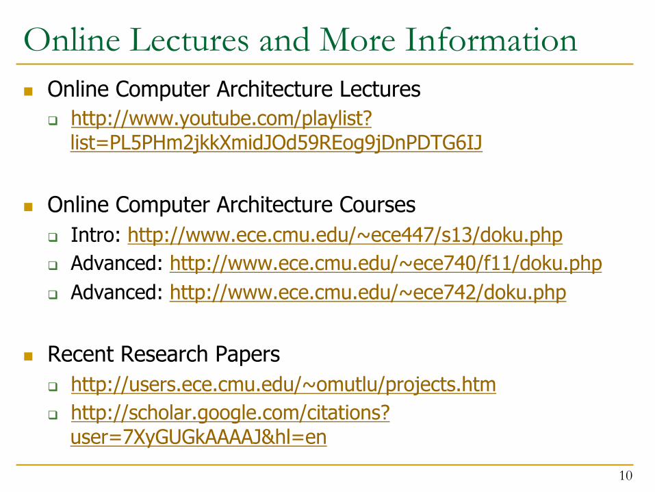
Online Lectures and More Information n Online Computer Architecture Lectures
n Major Trends Affecting Main Memory n Requirements from an Ideal Main Memory System n Opportunity: Emerging Memory Technologies n Conclusions n Discussion
12
Major Trends Affecting Main Memory (I) n Need for main memory capacity and bandwidth increasing
n Main memory energy/power is a key system design concern
n DRAM technology scaling is ending
13
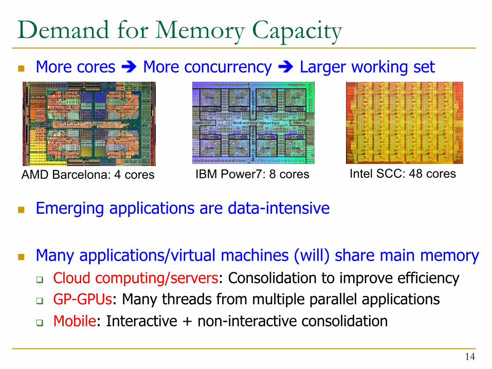
Demand for Memory Capacity n More cores è More concurrency è Larger working set
n Emerging applications are data-intensive
n Many applications/virtual machines (will) share main memory
q Cloud computing/servers: Consolidation to improve efficiency q GP-GPUs: Many threads from multiple parallel applications q Mobile: Interactive + non-interactive consolidation
n Memory capacity per core expected to drop by 30% every two years
15
Core count doubling ~ every 2 years DRAM DIMM capacity doubling ~ every 3 years
Major Trends Affecting Main Memory (II) n Need for main memory capacity and bandwidth increasing
q Multi-core: increasing number of cores q Data-intensive applications: increasing demand/hunger for data q Consolidation: Cloud computing, GPUs, mobile
n Main memory energy/power is a key system design concern
n DRAM technology scaling is ending
16
Major Trends Affecting Main Memory (III) n Need for main memory capacity and bandwidth increasing
n Main memory energy/power is a key system design concern
q IBM servers: ~50% energy spent in off-chip memory hierarchy [Lefurgy, IEEE Computer 2003]
q DRAM consumes power when idle and needs periodic refresh
n DRAM technology scaling is ending
17
Major Trends Affecting Main Memory (IV) n Need for main memory capacity and bandwidth increasing
n Main memory energy/power is a key system design concern
n DRAM technology scaling is ending
q ITRS projects DRAM will not scale easily below 40nm q Scaling has provided many benefits:
n higher capacity, higher density, lower cost, lower energy
18
The DRAM Scaling Problem n DRAM stores charge in a capacitor (charge-based memory)
q Capacitor must be large enough for reliable sensing q Access transistor should be large enough for low leakage and high
retention time q Scaling beyond 40-35nm (2013) is challenging [ITRS, 2009]
n DRAM capacity, cost, and energy/power hard to scale
19
Trends: Problems with DRAM as Main Memory
n Need for main memory capacity and bandwidth increasing q DRAM capacity hard to scale
n Main memory energy/power is a key system design concern
q DRAM consumes high power due to leakage and refresh
n DRAM technology scaling is ending
q DRAM capacity, cost, and energy/power hard to scale
20
Agenda
n Major Trends Affecting Main Memory n Requirements from an Ideal Main Memory System n Opportunity: Emerging Memory Technologies n Conclusions n Discussion
21
n Traditional q Enough capacity q Low cost q High system performance (high bandwidth, low latency)
n New q Technology scalability: lower cost, higher capacity, lower energy q Energy (and power) efficiency q QoS support and configurability (for consolidation)
22
Requirements from an Ideal Memory System
n Traditional q Higher capacity q Continuous low cost q High system performance (higher bandwidth, low latency)
n New q Technology scalability: lower cost, higher capacity, lower energy q Energy (and power) efficiency q QoS support and configurability (for consolidation)
23
Requirements from an Ideal Memory System
Emerging, resistive memory technologies (NVM) can help
Agenda
n Major Trends Affecting Main Memory n Requirements from an Ideal Main Memory System n Opportunity: Emerging Memory Technologies n Conclusions n Discussion
24
The Promise of Emerging Technologies
n Likely need to replace/augment DRAM with a technology that is q Technology scalable q And at least similarly efficient, high performance, and fault-tolerant
n or can be architected to be so
n Some emerging resistive memory technologies appear promising q Phase Change Memory (PCM)? q Spin Torque Transfer Magnetic Memory (STT-MRAM)? q Memristors? q And, maybe there are other ones q Can they be enabled to replace/augment/surpass DRAM?
25
Agenda
n Major Trends Affecting Main Memory n Requirements from an Ideal Main Memory System n Opportunity: Emerging Memory Technologies
q Background q PCM (or Technology X) as DRAM Replacement q Hybrid Memory Systems
n Conclusions n Discussion
26
Charge vs. Resistive Memories
n Charge Memory (e.g., DRAM, Flash) q Write data by capturing charge Q q Read data by detecting voltage V
n Resistive Memory (e.g., PCM, STT-MRAM, memristors) q Write data by pulsing current dQ/dt q Read data by detecting resistance R
27
Limits of Charge Memory n Difficult charge placement and control
n Reliable sensing becomes difficult as charge storage unit size reduces
28
Emerging Resistive Memory Technologies n PCM
q Inject current to change material phase q Resistance determined by phase
n STT-MRAM q Inject current to change magnet polarity q Resistance determined by polarity
n Memristors q Inject current to change atomic structure q Resistance determined by atom distance
29
What is Phase Change Memory? n Phase change material (chalcogenide glass) exists in two states:
q Amorphous: Low optical reflexivity and high electrical resistivity q Crystalline: High optical reflexivity and low electrical resistivity
30
PCM is resistive memory: High resistance (0), Low resistance (1) PCM cell can be switched between states reliably and quickly
How Does PCM Work? n Write: change phase via current injection
q SET: sustained current to heat cell above Tcryst q RESET: cell heated above Tmelt and quenched
n Read: detect phase via material resistance q amorphous/crystalline
31
Large Current
SET (cryst) Low resistance
103-104 Ω
Small Current
RESET (amorph) High resistance
Access Device
Memory Element
106-107 Ω
Photo Courtesy: Bipin Rajendran, IBM Slide Courtesy: Moinuddin Qureshi, IBM
Opportunity: PCM Advantages n Scales better than DRAM, Flash
q Requires current pulses, which scale linearly with feature size q Expected to scale to 9nm (2022 [ITRS]) q Prototyped at 20nm (Raoux+, IBM JRD 2008)
n Can be denser than DRAM q Can store multiple bits per cell due to large resistance range q Prototypes with 2 bits/cell in ISSCC’08, 4 bits/cell by 2012
n Non-volatile q Retain data for >10 years at 85C
n No refresh needed, low idle power 32
Phase Change Memory Properties
n Surveyed prototypes from 2003-2008 (ITRS, IEDM, VLSI, ISSCC)
n Derived PCM parameters for F=90nm
n Lee, Ipek, Mutlu, Burger, “Architecting Phase Change Memory as a Scalable DRAM Alternative,” ISCA 2009.
33
34
Phase Change Memory Properties: Latency n Latency comparable to, but slower than DRAM
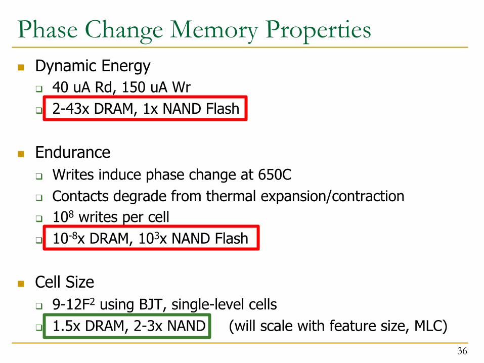
n Endurance q Writes induce phase change at 650C q Contacts degrade from thermal expansion/contraction q 108 writes per cell q 10-8x DRAM, 103x NAND Flash
n Cell Size q 9-12F2 using BJT, single-level cells q 1.5x DRAM, 2-3x NAND (will scale with feature size, MLC)
36
Phase Change Memory: Pros and Cons n Pros over DRAM
q Better technology scaling q Non volatility q Low idle power (no refresh)
n Cons q Higher latencies: ~4-15x DRAM (especially write) q Higher active energy: ~2-50x DRAM (especially write) q Lower endurance (a cell dies after ~108 writes)
n Challenges in enabling PCM as DRAM replacement/helper: q Mitigate PCM shortcomings q Find the right way to place PCM in the system q Ensure secure and fault-tolerant PCM operation
37
PCM-based Main Memory: Research Challenges n Where to place PCM in the memory hierarchy?
q Hybrid OS controlled PCM-DRAM q Hybrid OS controlled PCM and hardware-controlled DRAM q Pure PCM main memory
n How to mitigate shortcomings of PCM?
n How to minimize amount of DRAM in the system?
n How to take advantage of (byte-addressable and fast) non-volatile main memory?
n Can we design specific-NVM-technology-agnostic techniques? 38
PCM-based Main Memory (I) n How should PCM-based (main) memory be organized?
n Hybrid PCM+DRAM [Qureshi+ ISCA’09, Dhiman+ DAC’09, Meza+ IEEE CAL’12]: q How to partition/migrate data between PCM and DRAM
39
Hybrid Memory Systems: Challenges
n Partitioning q Should DRAM be a cache or main memory, or configurable? q What fraction? How many controllers?
n Data allocation/movement (energy, performance, lifetime) q Who manages allocation/movement? q What are good control algorithms? q How do we prevent degradation of service due to wearout?
n Design of cache hierarchy, memory controllers, OS q Mitigate PCM shortcomings, exploit PCM advantages
n Design of PCM/DRAM chips and modules q Rethink the design of PCM/DRAM with new requirements
40
PCM-based Main Memory (II) n How should PCM-based (main) memory be organized?
n Pure PCM main memory [Lee et al., ISCA’09, Top Picks’10]:
q How to redesign entire hierarchy (and cores) to overcome PCM shortcomings
41
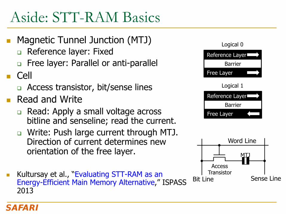
Aside: STT-RAM Basics n Magnetic Tunnel Junction (MTJ)
q Reference layer: Fixed q Free layer: Parallel or anti-parallel
n Cell q Access transistor, bit/sense lines
n Read and Write q Read: Apply a small voltage across
bitline and senseline; read the current. q Write: Push large current through MTJ.
Direction of current determines new orientation of the free layer.
n Kultursay et al., “Evaluating STT-RAM as an Energy-Efficient Main Memory Alternative,” ISPASS 2013
Reference Layer
Free Layer
Barrier
Reference Layer
Free Layer
Barrier
Logical 0
Logical 1
Word Line
Bit Line
Access Transistor
MTJ
Sense Line
Aside: STT MRAM: Pros and Cons n Pros over DRAM
q Better technology scaling q Non volatility q Low idle power (no refresh)
n Cons q Higher write latency q Higher write energy q Reliability?
n Another level of freedom q Can trade off non-volatility for lower write latency/energy (by
reducing the size of the MTJ)
43
Agenda
n Major Trends Affecting Main Memory n Requirements from an Ideal Main Memory System n Opportunity: Emerging Memory Technologies
q Background q PCM (or Technology X) as DRAM Replacement q Hybrid Memory Systems
n Conclusions n Discussion
44
An Initial Study: Replace DRAM with PCM n Lee, Ipek, Mutlu, Burger, “Architecting Phase Change
Memory as a Scalable DRAM Alternative,” ISCA 2009. q Surveyed prototypes from 2003-2008 (e.g. IEDM, VLSI, ISSCC) q Derived “average” PCM parameters for F=90nm
45
Results: Naïve Replacement of DRAM with PCM n Replace DRAM with PCM in a 4-core, 4MB L2 system n PCM organized the same as DRAM: row buffers, banks, peripherals n 1.6x delay, 2.2x energy, 500-hour average lifetime
n Lee, Ipek, Mutlu, Burger, “Architecting Phase Change Memory as a
Scalable DRAM Alternative,” ISCA 2009. 46
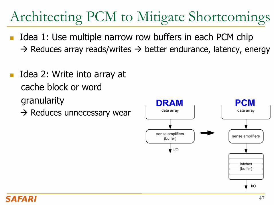
Architecting PCM to Mitigate Shortcomings n Idea 1: Use multiple narrow row buffers in each PCM chip
à Reduces array reads/writes à better endurance, latency, energy
n Idea 2: Write into array at cache block or word granularity
à Reduces unnecessary wear
47
DRAM PCM
Results: Architected PCM as Main Memory n 1.2x delay, 1.0x energy, 5.6-year average lifetime n Scaling improves energy, endurance, density
n Caveat 1: Worst-case lifetime is much shorter (no guarantees) n Caveat 2: Intensive applications see large performance and energy hits n Caveat 3: Optimistic PCM parameters?
48
The image cannot be displayed. Your computer may not have enough memory to open the image, or the image may have been corrupted. Restart your computer, and then open the file again. If the red x still appears, you may have to delete the image and then insert it again.
Agenda
n Major Trends Affecting Main Memory n Requirements from an Ideal Main Memory System n Opportunity: Emerging Memory Technologies
q Background q PCM (or Technology X) as DRAM Replacement q Hybrid Memory Systems
Large, non-volatile, low-cost Slow, wears out, high active energy
PCM Ctrl DRAM Phase Change Memory (or Tech. X)
Hardware/software manage data allocation and movement to achieve the best of multiple technologies
One Option: DRAM as a Cache for PCM n PCM is main memory; DRAM caches memory rows/blocks
q Benefits: Reduced latency on DRAM cache hit; write filtering
n Memory controller hardware manages the DRAM cache q Benefit: Eliminates system software overhead
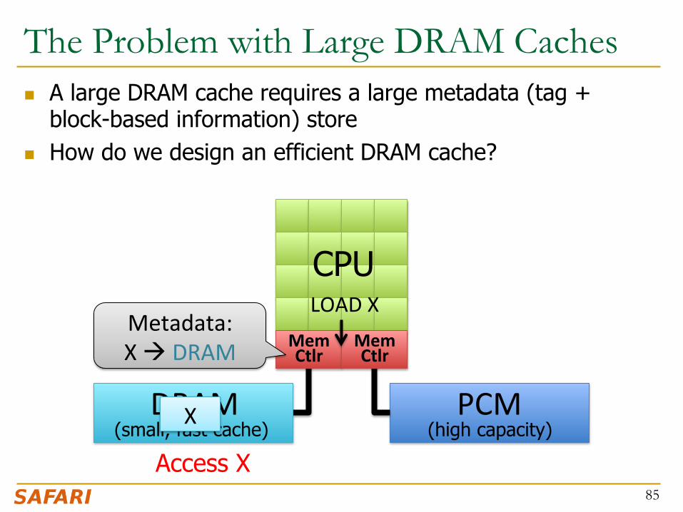
n Three issues: q What data should be placed in DRAM versus kept in PCM? q What is the granularity of data movement? q How to design a low-cost hardware-managed DRAM cache?
n Two idea directions: q Locality-aware data placement [Yoon+ , ICCD 2012]
q Cheap tag stores and dynamic granularity [Meza+, IEEE CAL 2012]
51
DRAM as a Cache for PCM n Goal: Achieve the best of both DRAM and PCM/NVM
q Minimize amount of DRAM w/o sacrificing performance, endurance q DRAM as cache to tolerate PCM latency and write bandwidth q PCM as main memory to provide large capacity at good cost and power
52
DATA
PCM Main Memory
DATA T
DRAM Buffer
PCM Write Queue
T=Tag-Store
Processor
Flash Or
HDD
Write Filtering Techniques n Lazy Write: Pages from disk installed only in DRAM, not PCM n Partial Writes: Only dirty lines from DRAM page written back n Page Bypass: Discard pages with poor reuse on DRAM eviction
n Qureshi et al., “Scalable high performance main memory system using phase-change memory technology,” ISCA 2009.
53
Processor
DATA PCM Main Memory
DATA T
DRAM Buffer Flash
Or HDD
Results: DRAM as PCM Cache (I) n Simulation of 16-core system, 8GB DRAM main-memory at 320 cycles,
HDD (2 ms) with Flash (32 us) with Flash hit-rate of 99% n Assumption: PCM 4x denser, 4x slower than DRAM n DRAM block size = PCM page size (4kB)
Results: DRAM as PCM Cache (II) n PCM-DRAM Hybrid performs similarly to similar-size DRAM n Significant power and energy savings with PCM-DRAM Hybrid n Average lifetime: 9.7 years (no guarantees)
55
0
0.2
0.4
0.6
0.8
1
1.2
1.4
1.6
1.8
2
2.2
Power Energy Energy x Delay
Valu
e N
orm
aliz
ed to
8G
B D
RA
M 8GB DRAMHybrid (32GB PCM+ 1GB DRAM)32GB DRAM
Agenda
n Major Trends Affecting Main Memory n Requirements from an Ideal Main Memory System n Opportunity: Emerging Memory Technologies
q Background q PCM (or Technology X) as DRAM Replacement q Hybrid Memory Systems
n Row-Locality Aware Data Placement n Efficient DRAM (or Technology X) Caches
n Conclusions n Discussion
56
Row Buffer Locality Aware���Caching Policies for Hybrid Memories
Benefit 1: Increased row buffer locality (RBL) in PCM by moving low RBL data to DRAM
17%
Benefit 1: Increased row buffer locality (RBL) in PCM by moving low RBL data to DRAM Benefit 2: Reduced memory bandwidth
consump?on due to stricter caching criteria Benefit 2: Reduced memory bandwidth
consump?on due to stricter caching criteria Benefit 3: Balanced memory request load
between DRAM and PCM
0
0.2
0.4
0.6
0.8
1
1.2
Server Cloud Avg
Nor
mal
ized
Avg
Mem
ory
Lat
ency
Workload
FREQ FREQ-Dyn RBLA RBLA-Dyn
Average Memory Latency
77
14%
9% 12%
0
0.2
0.4
0.6
0.8
1
1.2
Server Cloud Avg
Nor
mal
ized
Per
f. pe
r Wat
t
Workload
FREQ FREQ-Dyn RBLA RBLA-Dyn
Memory Energy Efficiency
78
Increased performance & reduced data movement between DRAM and PCM
7% 10% 13%
0
0.2
0.4
0.6
0.8
1
1.2
Server Cloud Avg
Nor
mal
ized
Max
imum
Slo
wdo
wn
Workload
FREQ FREQ-Dyn RBLA RBLA-Dyn
Thread Fairness
79
7.6%
4.8% 6.2%
0 0.2 0.4 0.6 0.8
1 1.2 1.4 1.6 1.8
2
Weighted Speedup Max. Slowdown Perf. per Watt Normalized Metric
16GB PCM RBLA-Dyn 16GB DRAM
0 0.2 0.4 0.6 0.8
1 1.2 1.4 1.6 1.8
2
Nor
mal
ized
Wei
ghte
d Sp
eedu
p
0
0.2
0.4
0.6
0.8
1
1.2
Nor
mal
ized
Max
. Slo
wdo
wn
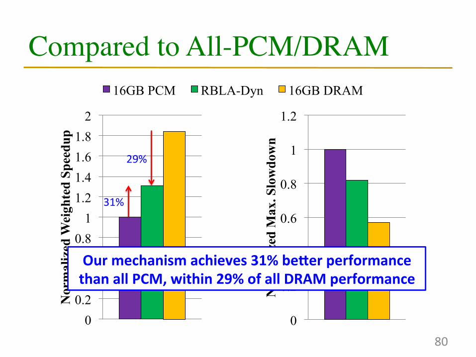
Compared to All-PCM/DRAM
80
Our mechanism achieves 31% beSer performance than all PCM, within 29% of all DRAM performance
31%
29%
Other Results in Paper • RBLA-‐Dyn increases the por,on of PCM row buffer hit by 6.6 ,mes
• RBLA-‐Dyn has the effect of balancing memory request load between DRAM and PCM – PCM channel u,liza,on increases by 60%.
81
Summary
82
• Different memory technologies have different strengths • A hybrid memory system (DRAM-‐PCM) aims for best of both • Problem: How to place data between these heterogeneous
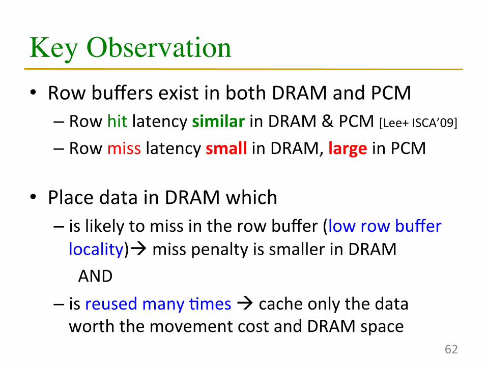
memory devices? • Observa?on: PCM array access latency is higher than
DRAM’s – But peripheral circuit (row buffer) access latencies are similar
• Key Idea: Use row buffer locality (RBL) as a key criterion for data placement
• Solu?on: Cache to DRAM rows with low RBL and high reuse • Improves both performance and energy efficiency over
state-‐of-‐the-‐art caching policies
Row Buffer Locality Aware���Caching Policies for Hybrid Memories
Idea 2: Cache Tags in SRAM n Recall Idea 1: Store all metadata in DRAM
q To reduce metadata storage overhead
n Idea 2: Cache in on-chip SRAM frequently-accessed metadata q Cache only a small amount to keep SRAM size small
87
Idea 3: Dynamic Data Transfer Granularity n Some applications benefit from caching more data
q They have good spatial locality
n Others do not q Large granularity wastes bandwidth and reduces cache
utilization
n Idea 3: Simple dynamic caching granularity policy q Cost-benefit analysis to determine best DRAM cache block size q Group main memory into sets of rows q Some row sets follow a fixed caching granularity q The rest of main memory follows the best granularity
n Cost–benefit analysis: access latency versus number of cachings n Performed every quantum
88
TIMBER Tag Management n A Tag-In-Memory BuffER (TIMBER)
q Stores recently-used tags in a small amount of SRAM
n Benefits: If tag is cached:
q no need to access DRAM twice q cache hit determined quickly
TIMBER Tag Management Example (I) n Case 1: TIMBER hit
90
Bank Bank Bank Bank
CPU
Mem Ctlr
Mem Ctlr
LOAD X
TIMBER: X à DRAM
X
Access X
Tag0 Tag1 Tag2 Row0
Tag0 Tag1 Tag2 Row27
Our proposal
TIMBER Tag Management Example (II) n Case 2: TIMBER miss
91
CPU
Mem Ctlr
Mem Ctlr
LOAD Y
Y à DRAM
Bank Bank Bank Bank
Access Metadata(Y)
Y
1. Access M(Y)
Tag0 Tag1 Tag2 Row0
Tag0 Tag1 Tag2 Row27
Miss
M(Y)
2. Cache M(Y)
Row143
3. Access Y (row hit)
Methodology n System: 8 out-of-order cores at 4 GHz
n Memory: 512 MB direct-mapped DRAM, 8 GB PCM q 128B caching granularity q DRAM row hit (miss): 200 cycles (400 cycles) q PCM row hit (clean / dirty miss): 200 cycles (640 / 1840 cycles)
n Evaluated metadata storage techniques q All SRAM system (8MB of SRAM) q Region metadata storage q TIM metadata storage (same row as data) q TIMBER, 64-entry direct-mapped (8KB of SRAM)
92
93
Metadata Storage Performance
0 0.1 0.2 0.3 0.4 0.5 0.6 0.7 0.8 0.9 1
SRAM Region TIM TIMBER
Normalized
Weighted Speedu
p
(Ideal)
0 0.1 0.2 0.3 0.4 0.5 0.6 0.7 0.8 0.9 1
SRAM Region TIM TIMBER
Normalized
Weighted Speedu
p
94
Metadata Storage Performance
-‐48%
Performance degrades due to increased metadata lookup access latency
(Ideal)
0 0.1 0.2 0.3 0.4 0.5 0.6 0.7 0.8 0.9 1
SRAM Region TIM TIMBER
Normalized
Weighted Speedu
p
95
Metadata Storage Performance
36%
Increased row locality reduces average
memory access latency
(Ideal)
0 0.1 0.2 0.3 0.4 0.5 0.6 0.7 0.8 0.9 1
SRAM Region TIM TIMBER
Normalized
Weighted Speedu
p
96
Metadata Storage Performance
23% Data with locality can access metadata at SRAM latencies
Enabling and Exploiting NVM: Issues n Many issues and ideas from
technology layer to algorithms layer
n Enabling NVM and hybrid memory q How to tolerate errors? q How to enable secure operation? q How to tolerate performance and
power shortcomings? q How to minimize cost?
n Exploiting emerging technologies q How to exploit non-volatility? q How to minimize energy consumption? q How to exploit NVM on chip?
100
Microarchitecture
ISA
Programs
Algorithms Problems
Logic
Devices
Runtime System (VM, OS, MM)
User
Security Challenges of Emerging Technologies
1. Limited endurance à Wearout attacks 2. Non-volatility à Data persists in memory after powerdown à Easy retrieval of privileged or private information 3. Multiple bits per cell à Information leakage (via side channel)
101
Securing Emerging Memory Technologies
1. Limited endurance à Wearout attacks Better architecting of memory chips to absorb writes Hybrid memory system management Online wearout attack detection 2. Non-volatility à Data persists in memory after powerdown à Easy retrieval of privileged or private information Efficient encryption/decryption of whole main memory Hybrid memory system management 3. Multiple bits per cell à Information leakage (via side channel) System design to hide side channel information
102
Agenda
n Major Trends Affecting Main Memory n Requirements from an Ideal Main Memory System n Opportunity: Emerging Memory Technologies
q Background q PCM (or Technology X) as DRAM Replacement q Hybrid Memory Systems
n Conclusions n Discussion
103
Summary: Memory Scaling (with NVM) n Main memory scaling problems are a critical bottleneck for
system performance, efficiency, and usability
n Solution 1: Tolerate DRAM (yesterday)
n Solution 2: Enable emerging memory technologies q Replace DRAM with NVM by architecting NVM chips well q Hybrid memory systems with automatic data management
n An exciting topic with many other solution directions & ideas q Hardware/software/device cooperation essential q Memory, storage, controller, software/app co-design needed q Coordinated management of persistent memory and storage q Application and hardware cooperative management of NVM
104
Scalable Many-Core Memory Systems Topic 2: Emerging Technologies and
Overview Papers on Two Topics n Merging of Memory and Storage
q Justin Meza, Yixin Luo, Samira Khan, Jishen Zhao, Yuan Xie, and Onur Mutlu, "A Case for Efficient Hardware-Software Cooperative Management of Storage and Memory" Proceedings of the 5th Workshop on Energy-Efficient Design (WEED), Tel-Aviv, Israel, June 2013. Slides (pptx) Slides (pdf)
n Flash Memory Scaling
q Yu Cai, Gulay Yalcin, Onur Mutlu, Erich F. Haratsch, Adrian Cristal, Osman Unsal, and Ken Mai, "Error Analysis and Retention-Aware Error Management for NAND Flash Memory" Intel Technology Journal (ITJ) Special Issue on Memory Resiliency, Vol. 17, No. 1, May 2013.
107
Merging of Memory and Storage: Persistent Memory Managers
A Case for Efficient Hardware/Software Cooperative Management of
§Pennsylvania State University †Intel Labs ‡AMD Research
Overview n Traditional systems have a two-level storage model
q Access volatile data in memory with a load/store interface q Access persistent data in storage with a file system interface q Problem: Operating system (OS) and file system (FS) code and buffering
for storage lead to energy and performance inefficiencies
n Opportunity: New non-volatile memory (NVM) technologies can help provide fast (similar to DRAM), persistent storage (similar to Flash) q Unfortunately, OS and FS code can easily become energy efficiency and
performance bottlenecks if we keep the traditional storage model
n This work: makes a case for hardware/software cooperative management of storage and memory within a single-level q We describe the idea of a Persistent Memory Manager (PMM) for
efficiently coordinating storage and memory, and quantify its benefit q And, examine questions and challenges to address to realize PMM
110
Talk Outline n Background: Storage and Memory Models
n Motivation: Eliminating Operating/File System Bottlenecks
n Our Proposal: Hardware/Software Coordinated Management of
Storage and Memory
q Opportunities and Benefits
n Evaluation Methodology
n Evaluation Results
n Related Work
n New Questions and Challenges
n Conclusions
111
A Tale of Two Storage Levels n Traditional systems use a two-level storage model
q Volatile data is stored in DRAM q Persistent data is stored in HDD and Flash
n Accessed through two vastly different interfaces
112
Processor and caches
Main Memory Storage (SSD/HDD)
Virtual memory
Address translation
Load/Store
Operating system
and file system
fopen, fread, fwrite, …
A Tale of Two Storage Levels n Two-level storage arose in systems due to the widely different
access latencies and methods of the commodity storage devices q Fast, low capacity, volatile DRAM à working storage q Slow, high capacity, non-volatile hard disk drives à persistent storage
n Data from slow storage media is buffered in fast DRAM q After that it can be manipulated by programs à programs cannot
directly access persistent storage q It is the programmer’s job to translate this data between the two
formats of the two-level storage (files and data structures)
n Locating, transferring, and translating data and formats between the two levels of storage can waste significant energy and performance
113
Opportunity: New Non-Volatile Memories n Emerging memory technologies provide the potential for unifying
storage and memory (e.g., Phase-Change, STT-RAM, RRAM) q Byte-addressable (can be accessed like DRAM) q Low latency (comparable to DRAM) q Low power (idle power better than DRAM) q High capacity (closer to Flash) q Non-volatile (can enable persistent storage) q May have limited endurance (but, better than Flash)
n Can provide fast access to both volatile data and persistent storage
n Question: if such devices are used, is it efficient to keep a two-level storage model?
114
Eliminating Traditional Storage Bottlenecks
115
Normalized Total Energy
0
0.2
0.4
0.6
0.8
1.0
HDD Baseline NVM Baseline Persistent Memory
Frac
tion
of T
otal
Ene
rgy
0.0650.013
Today (DRAM + HDD) and two-level storage model Replace HDD
with NVM (PCM-like),
keep two-level storage model
Replace HDD and DRAM with NVM
(PCM-like), eliminate all
OS+FS overhead
Results for PostMark
Eliminating Traditional Storage Bottlenecks
116
0
0.2
0.4
0.6
0.8
1.0
HDD Baseline NVM Baseline Persistent Memory
Frac
tion
of T
otal
Ene
rgy
User CPU Syscall CPU DRAM NVM HDD
0.0650.013
Results for PostMark
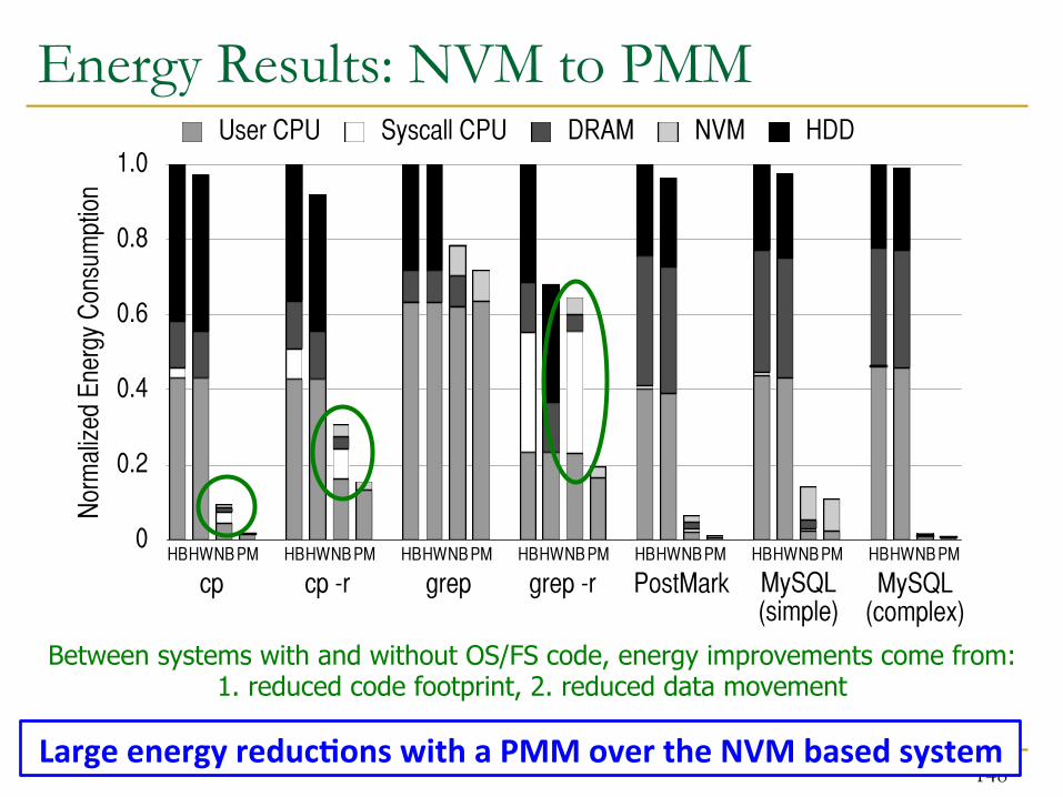
Where is Energy Spent in Each Model?
117
0
0.2
0.4
0.6
0.8
1.0
HDD Baseline NVM Baseline Persistent Memory
Frac
tion
of T
otal
Ene
rgy
User CPU Syscall CPU DRAM NVM HDD
HDD access wastes energy
FS/OS overhead becomes important
Additional DRAM energy due to buffering overhead
of two-level model
No FS/OS overhead No additional buffering
overhead in DRAM
Results for PostMark
Outline n Background: Storage and Memory Models
n Motivation: Eliminating Operating/File System Bottlenecks
n Our Proposal: Hardware/Software Coordinated Management of
Storage and Memory
q Opportunities and Benefits
n Evaluation Methodology
n Evaluation Results
n Related Work
n New Questions and Challenges
n Conclusions
118
Our Proposal: Coordinated HW/SW Memory and Storage Management
n Goal: Unify memory and storage to eliminate wasted work to locate, transfer, and translate data q Improve both energy and performance q Simplify programming model as well
119
Our Proposal: Coordinated HW/SW Memory and Storage Management
n Goal: Unify memory and storage to eliminate wasted work to locate, transfer, and translate data q Improve both energy and performance q Simplify programming model as well
120
Before: Traditional Two-Level Store
Processor and caches
Main Memory Storage (SSD/HDD)
Virtual memory
Address translation
Load/Store
Operating system
and file system
fopen, fread, fwrite, …
Our Proposal: Coordinated HW/SW Memory and Storage Management
n Goal: Unify memory and storage to eliminate wasted work to locate, transfer, and translate data q Improve both energy and performance q Simplify programming model as well
121
After: Coordinated HW/SW Management
Processor and caches
Persistent (e.g., Phase-Change) Memory
Load/Store
Persistent Memory Manager
Feedback
The Persistent Memory Manager (PMM) n Exposes a load/store interface to access persistent data
q Applications can directly access persistent memory à no conversion, translation, location overhead for persistent data
n Manages data placement, location, persistence, security q To get the best of multiple forms of storage
n Manages metadata storage and retrieval q This can lead to overheads that need to be managed
n Exposes hooks and interfaces for system software q To enable better data placement and management decisions
122
The Persistent Memory Manager n Persistent Memory Manager
q Exposes a load/store interface to access persistent data q Manages data placement, location, persistence, security q Manages metadata storage and retrieval q Exposes hooks and interfaces for system software
n Example program manipulating a persistent object:
123
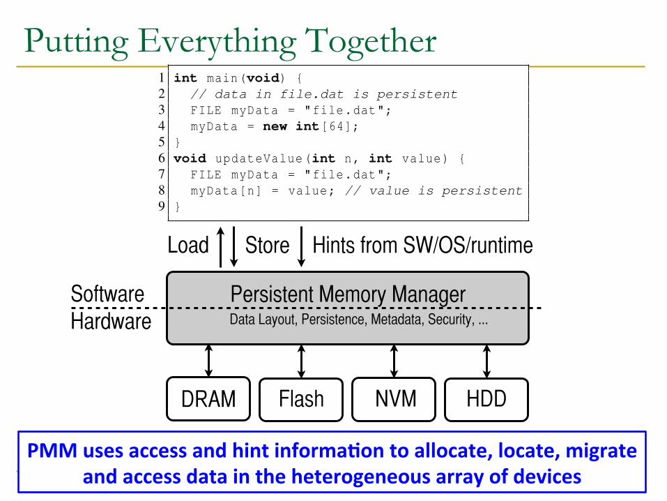
2.2.1 Efficient Hardware and Software Support: We propose to investigate the efficient software andhardware support needed for single-level stores. A single-level store system should provide an abstractionthat maps persistent user data to physical addresses in memory. A software interface for programs wouldmap a pointer to the actual persistent data. Programs would be able to access any part of the data usingnormal load and store instructions. Figure 2 shows two examples of high-level abstractions which couldbe provided to programs to access persistent data in a single-level store system. In it, a program createsa persistent file (Figure 2 left) or object (Figure 2 right) using the handle “file.dat” and allocates an arrayof integers in it. Later—perhaps after the application or system is restarted—when the program executesthe updateValue() function, the system retrieves the persistent data for the same handle, and the programmodifies its state. With such an abstraction, a single-level store can eliminate the OS system calls to transferdata to and from disk. In addition, it eliminates the need for a file system to track physical file addressesby traversing metadata (such as inodes) in the OS. In this way, single-level stores provide the opportunity todesign a simple and efficient persistent data lookup system in hardware. We plan to research efficient waysto map files or objects to the virtual address space. In such a hardware-based design, the processor wouldmanage how data handles correspond to physical addresses. Note that, single-level stores can use alternativedesign choices, such as segments, to provide the high-level abstraction instead of files or objects. Regardless,segments, files, or objects will be mapped to physical addresses with hardware support. Prior works tried tomake file lookup and update efficient in software [27, 28] in the presence of persistent memory, and otherworks proposed using complex and potentially inefficient hardware directory techniques (e.g., [15]). Ourgoal is to design fast and efficient techniques that take into account the byte addressability of persistentmemory in a single-level store. To this end, we will research the following:• The efficient use of hash table and B-tree indices for locating files in a single-level store.• How techniques such as key-value stores can provide fast and efficient lookups in single-level stores.• Policies for intelligently caching some entries of these indices in hardware to improve system perfor-
mance.Every access in the single-level store needs to be translated from a virtual address used by a program to
a physical address used to access a device. We will investigate how to efficiently manage address translationso that locating data is simple and fast. We intend to explore the following directions to solve this problem:• We will design mechanisms to predict access patterns based on program behavior and pre-compute
virtual-to-physical address translations. We are interested in answering questions such as: What is thepattern of data accesses to a single-level store, and how can prefetching techniques be redesigned withsingle-level stores in mind to enable efficient address translation? How can simple application-level orprofile-based hints on access patterns be communicated to and used by hardware to make address translationand prefetching efficient?• We will design efficient translation lookaside buffer (TLB)-like structures which will cache the trans-
lation between virtual and physical addresses but for a much larger amount of physical memory than inexisting systems. In the presence of such a single-level store, many disparate data accesses could need alarge translation table to be serviced effectively. To reduce overhead of such hardware, we are interested inexploring whether TLB-like structures should favor storing translations only for particular classes of data,such as data with locality or data which is on the critical path of execution, which get the most benefitout of the limited structure space. In addition, we will investigate centralized versus distributed translationstructures to design techniques that, for example, buffer private data translation entries near the processor,while distributing shared entries across processors to minimize translation overheads. Such translation struc-
1 int main(void) {2 // data in file.dat is persistent3 FILE myData = "file.dat";4 myData = new int[64];5 }6 void updateValue(int n, int value) {7 FILE myData = "file.dat";8 myData[n] = value; // value is persistent9 }
1 int main(void) {2 // data in file.dat is persistent3 int *myData = new PersistentObject("file.dat");4 myData = new int[64];5 }6 void updateValue(int n, int value) {7 int *myData = PersistentObject.open("file.dat");8 myData[n] = value; // value is persistent9 }
Figure 2: Sample program with access to file-based (left) and object-based (right) persistent data.
5
Create persistent object and its handle Allocate a persistent array and assign
Load/store interface
Putting Everything Together
124
2.2.1 Efficient Hardware and Software Support: We propose to investigate the efficient software andhardware support needed for single-level stores. A single-level store system should provide an abstractionthat maps persistent user data to physical addresses in memory. A software interface for programs wouldmap a pointer to the actual persistent data. Programs would be able to access any part of the data usingnormal load and store instructions. Figure 2 shows two examples of high-level abstractions which couldbe provided to programs to access persistent data in a single-level store system. In it, a program createsa persistent file (Figure 2 left) or object (Figure 2 right) using the handle “file.dat” and allocates an arrayof integers in it. Later—perhaps after the application or system is restarted—when the program executesthe updateValue() function, the system retrieves the persistent data for the same handle, and the programmodifies its state. With such an abstraction, a single-level store can eliminate the OS system calls to transferdata to and from disk. In addition, it eliminates the need for a file system to track physical file addressesby traversing metadata (such as inodes) in the OS. In this way, single-level stores provide the opportunity todesign a simple and efficient persistent data lookup system in hardware. We plan to research efficient waysto map files or objects to the virtual address space. In such a hardware-based design, the processor wouldmanage how data handles correspond to physical addresses. Note that, single-level stores can use alternativedesign choices, such as segments, to provide the high-level abstraction instead of files or objects. Regardless,segments, files, or objects will be mapped to physical addresses with hardware support. Prior works tried tomake file lookup and update efficient in software [27, 28] in the presence of persistent memory, and otherworks proposed using complex and potentially inefficient hardware directory techniques (e.g., [15]). Ourgoal is to design fast and efficient techniques that take into account the byte addressability of persistentmemory in a single-level store. To this end, we will research the following:• The efficient use of hash table and B-tree indices for locating files in a single-level store.• How techniques such as key-value stores can provide fast and efficient lookups in single-level stores.• Policies for intelligently caching some entries of these indices in hardware to improve system perfor-
mance.Every access in the single-level store needs to be translated from a virtual address used by a program to
a physical address used to access a device. We will investigate how to efficiently manage address translationso that locating data is simple and fast. We intend to explore the following directions to solve this problem:• We will design mechanisms to predict access patterns based on program behavior and pre-compute
virtual-to-physical address translations. We are interested in answering questions such as: What is thepattern of data accesses to a single-level store, and how can prefetching techniques be redesigned withsingle-level stores in mind to enable efficient address translation? How can simple application-level orprofile-based hints on access patterns be communicated to and used by hardware to make address translationand prefetching efficient?• We will design efficient translation lookaside buffer (TLB)-like structures which will cache the trans-
lation between virtual and physical addresses but for a much larger amount of physical memory than inexisting systems. In the presence of such a single-level store, many disparate data accesses could need alarge translation table to be serviced effectively. To reduce overhead of such hardware, we are interested inexploring whether TLB-like structures should favor storing translations only for particular classes of data,such as data with locality or data which is on the critical path of execution, which get the most benefitout of the limited structure space. In addition, we will investigate centralized versus distributed translationstructures to design techniques that, for example, buffer private data translation entries near the processor,while distributing shared entries across processors to minimize translation overheads. Such translation struc-
1 int main(void) {2 // data in file.dat is persistent3 FILE myData = "file.dat";4 myData = new int[64];5 }6 void updateValue(int n, int value) {7 FILE myData = "file.dat";8 myData[n] = value; // value is persistent9 }
1 int main(void) {2 // data in file.dat is persistent3 int *myData = new PersistentObject("file.dat");4 myData = new int[64];5 }6 void updateValue(int n, int value) {7 int *myData = PersistentObject.open("file.dat");8 myData[n] = value; // value is persistent9 }
Figure 2: Sample program with access to file-based (left) and object-based (right) persistent data.
PMM uses access and hint informa?on to allocate, locate, migrate and access data in the heterogeneous array of devices
Outline n Background: Storage and Memory Models
n Motivation: Eliminating Operating/File System Bottlenecks
n Our Proposal: Hardware/Software Coordinated Management of
Storage and Memory
q Opportunities and Benefits
n Evaluation Methodology
n Evaluation Results
n Related Work
n New Questions and Challenges
n Conclusions
125
Opportunities and Benefits
n We’ve identified at least five opportunities and benefits of a unified storage/memory system that gets rid of the two-level model:
1. Eliminating system calls for file operations
2. Eliminating file system operations
3. Efficient data mapping/location among heterogeneous devices
4. Providing security and reliability in persistent memories
5. Hardware/software cooperative data management
126
Eliminating System Calls for File Operations
n A persistent memory can expose a large, linear, persistent address space q Persistent storage objects can be directly manipulated with load/
store operations
n This eliminates the need for layers of operating system code q Typically used for calls like open, read, and write!
n Also eliminates OS file metadata q File descriptors, file buffers, and so on
127
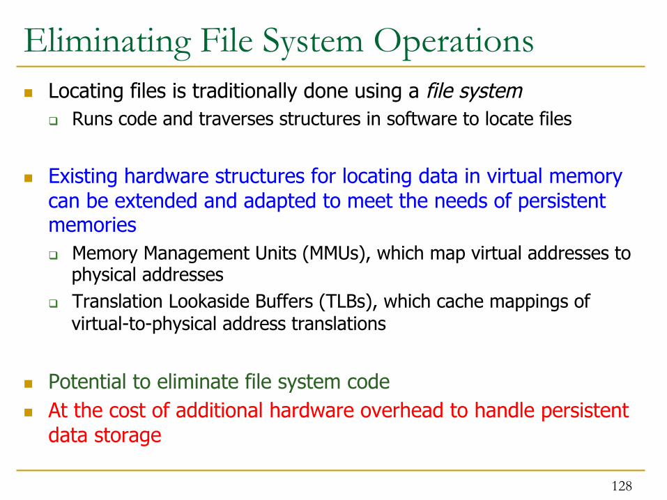
Eliminating File System Operations n Locating files is traditionally done using a file system
q Runs code and traverses structures in software to locate files
n Existing hardware structures for locating data in virtual memory can be extended and adapted to meet the needs of persistent memories q Memory Management Units (MMUs), which map virtual addresses to
physical addresses q Translation Lookaside Buffers (TLBs), which cache mappings of
virtual-to-physical address translations
n Potential to eliminate file system code n At the cost of additional hardware overhead to handle persistent
data storage
128
Efficient Data Mapping among Heterogeneous Devices
n A persistent memory exposes a large, persistent address space q But it may use many different devices to satisfy this goal q From fast, low-capacity volatile DRAM to slow, high-capacity non-
volatile HDD or Flash q And other NVM devices in between
n Performance and energy can benefit from good placement of data among these devices q Utilizing the strengths of each device and avoiding their weaknesses,
if possible q For example, consider two important application characteristics:
locality and persistence
129
130
Efficient Data Mapping among Heterogeneous Devices
131
X
Columns in a column store that are scanned through only infrequently
à place on Flash
Efficient Data Mapping among Heterogeneous Devices
132
X
Columns in a column store that are scanned through only infrequently
à place on Flash
X
Frequently-updated index for a Content Delivery Network (CDN)
à place in DRAM
Efficient Data Mapping among Heterogeneous Devices
Applica?ons or system so[ware can provide hints for data placement
Providing Security and Reliability
n A persistent memory deals with data at the granularity of bytes and not necessarily files q Provides the opportunity for much finer-grained security and
protection than traditional two-level storage models provide/afford q Need efficient techniques to avoid large metadata overheads
n A persistent memory can improve application reliability by ensuring updates to persistent data are less vulnerable to failures q Need to ensure that changes to copies of persistent data placed in
volatile memories become persistent
133
HW/SW Cooperative Data Management
n Persistent memories can expose hooks and interfaces to applications, the OS, and runtimes q Have the potential to provide improved system robustness and
efficiency than by managing persistent data with either software or hardware alone
n Can enable fast checkpointing and reboots, improve application reliability by ensuring persistence of data q How to redesign availability mechanisms to take advantage of these?
n Persistent locks and other persistent synchronization constructs can enable more robust programs and systems
134
Quantifying Persistent Memory Benefits
n We have identified several opportunities and benefits of using persistent memories without the traditional two-level store model
n We will next quantify: q How do persistent memories affect system performance? q How much energy reduction is possible? q Can persistent memories achieve these benefits despite additional
access latencies to the persistent memory manager?
135
Outline n Background: Storage and Memory Models
n Motivation: Eliminating Operating/File System Bottlenecks
n Our Proposal: Hardware/Software Coordinated Management of
Storage and Memory
q Opportunities and Benefits
n Evaluation Methodology
n Evaluation Results
n Related Work
n New Questions and Challenges
n Conclusions
136
Evaluation Methodology n Hybrid real system / simulation-based approach
q System calls are executed on host machine (functional correctness) and timed to accurately model their latency in the simulator
q Rest of execution is simulated in Multi2Sim (enables hardware-level exploration)
n Power evaluated using McPAT and memory power models
n 16 cores, 4-wide issue, 128-entry instruction window, 1.6 GHz
n Volatile memory: 4GB DRAM, 4KB page size, 100-cycle latency
n Persistent memory q HDD (measured): 4ms seek latency, 6Gbps bus rate
q Traditional system with volatile DRAM memory and persistent HDD storage q Overheads of operating system and file system code and buffering
n HDD without OS/FS (HW) q Same as HDD Baseline, but with the ideal elimination of all OS/FS overheads q System calls take 0 cycles (but HDD access takes normal latency)
n NVM Baseline (NB) q Same as HDD Baseline, but HDD is replaced with NVM q Still has OS/FS overheads of the two-level storage model
n Persistent Memory (PM) q Uses only NVM (no DRAM) to ensure full-system persistence q All data accessed using loads and stores q Does not waste energy on system calls q Data is manipulated directly on the NVM device
138
Evaluated Workloads n Unix utilities that manipulate files
q cp: copy a large file from one location to another q cp –r: copy files in a directory tree from one location to another q grep: search for a string in a large file q grep –r: search for a string recursively in a directory tree
n PostMark: an I/O-intensive benchmark from NetApp q Emulates typical access patterns for email, news, web commerce
n MySQL Server: a popular database management system q OLTP-style queries generated by Sysbench q MySQL (simple): single, random read to an entry q MySQL (complex): reads/writes 1 to 100 entries per transaction
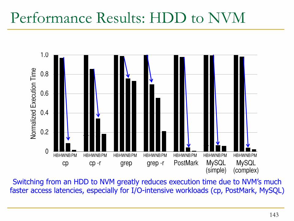
Though, for more complex file system operations like directory traversal (seen with cp -r and grep -r), eliminating the OS/FS overhead improves performance
Switching from an HDD to NVM greatly reduces execution time due to NVM’s much faster access latencies, especially for I/O-intensive workloads (cp, PostMark, MySQL)
The workloads that see the greatest improvement from using a Persistent Memory are those that spend a large portion of their time executing system call code due to
Large energy reduc?ons with a PMM over the NVM based system
Scalability Analysis: Effect of PMM Latency
149
Even if each PMM access takes a non-overlapped 50 cycles (conservative), PMM still provides an overall improvement compared to the NVM baseline
0
0.25
0.50
0.75
1.00
1.25
cp
cp -
r
grep
grep
-r
Pos
tMar
k
MyS
QL
(sim
ple)
MyS
QL
(com
plex
)
cp
cp -
r
grep
grep
-r
Pos
tMar
k
MyS
QL
(sim
ple)
MyS
QL
(com
plex
)
cp
cp -
r
grep
grep
-r
Pos
tMar
k
MyS
QL
(sim
ple)
MyS
QL
(com
plex
)
cp
cp -
r
grep
grep
-r
Pos
tMar
k
MyS
QL
(sim
ple)
MyS
QL
(com
plex
)
Nor
mal
ized
Exe
cutio
n T
ime
User CPU User Memory Syscall CPU Syscall I/O PMM
1 cycle 10 cycles 50 cyclesNB
1.53
Future research should target keeping PMM latencies in check
Outline n Background: Storage and Memory Models
n Motivation: Eliminating Operating/File System Bottlenecks
n Our Proposal: Hardware/Software Coordinated Management of
Storage and Memory
q Opportunities and Benefits
n Evaluation Methodology
n Evaluation Results
n Related Work
n New Questions and Challenges
n Conclusions
150
Related Work n We provide a comprehensive overview of past work related to
single-level stores and persistent memory techniques
1. Integrating file systems with persistent memory q Need optimized hardware to fully take advantage of new technologies
2. Programming language support for persistent objects q Incurs the added latency of indirect data access through software
3. Load/store interfaces to persistent storage q Lack efficient and fast hardware support for address translation, efficient
file indexing, fast reliability and protection guarantees
4. Analysis of OS overheads with Flash devices q Our study corroborates findings in this area and shows even larger
consequences for systems with emerging NVM devices
n The goal of our work is to provide cheap and fast hardware support for memories to enable high energy efficiency and performance
151
Outline n Background: Storage and Memory Models
n Motivation: Eliminating Operating/File System Bottlenecks
n Our Proposal: Hardware/Software Coordinated Management of
Storage and Memory
q Opportunities and Benefits
n Evaluation Methodology
n Evaluation Results
n Related Work
n New Questions and Challenges
n Conclusions
152
New Questions and Challenges n We identify and discuss several open research questions
Ø Q1. How to tailor applications for systems with persistent memory?
Ø Q2. How can hardware and software cooperate to support a scalable, persistent single-level address space?
Ø Q3. How to provide efficient backward compatibility (for two-level stores) on persistent memory systems?
Ø Q4. How to mitigate potential hardware performance and energy overheads?
153
Outline n Background: Storage and Memory Models
n Motivation: Eliminating Operating/File System Bottlenecks
n Our Proposal: Hardware/Software Coordinated Management of
Storage and Memory
q Opportunities and Benefits
n Evaluation Methodology
n Evaluation Results
n Related Work
n New Questions and Challenges
n Conclusions
154
Summary and Conclusions n Traditional two-level storage model is inefficient in terms of
performance and energy q Due to OS/FS code and buffering needed to manage two models q Especially so in future devices with NVM technologies, as we show
n New non-volatile memory based persistent memory designs that use a single-level storage model to unify memory and storage can alleviate this problem
n We quantified the performance and energy benefits of such a single-level persistent memory/storage design q Showed significant benefits from reduced code footprint, data
movement, and system software overhead on a variety of workloads
n Such a design requires more research to answer the questions we have posed and enable efficient persistent memory managers à can lead to a fundamentally more efficient storage system
155
A Case for Efficient Hardware/Software Cooperative Management of
§Pennsylvania State University †Intel Labs ‡AMD Research
Flash Memory Scaling
Readings in Flash Memory n Yu Cai, Gulay Yalcin, Onur Mutlu, Erich F. Haratsch, Adrian Cristal, Osman Unsal, and Ken Mai,
"Error Analysis and Retention-Aware Error Management for NAND Flash Memory" Intel Technology Journal (ITJ) Special Issue on Memory Resiliency, Vol. 17, No. 1, May 2013.
n Yu Cai, Erich F. Haratsch, Onur Mutlu, and Ken Mai, "Threshold Voltage Distribution in MLC NAND Flash Memory: Characterization, Analysis and Modeling" Proceedings of the Design, Automation, and Test in Europe Conference (DATE), Grenoble, France, March 2013. Slides (ppt)
n Yu Cai, Gulay Yalcin, Onur Mutlu, Erich F. Haratsch, Adrian Cristal, Osman Unsal, and Ken Mai, "Flash Correct-and-Refresh: Retention-Aware Error Management for Increased Flash Memory Lifetime" Proceedings of the 30th IEEE International Conference on Computer Design (ICCD), Montreal, Quebec, Canada, September 2012. Slides (ppt) (pdf)
n Yu Cai, Erich F. Haratsch, Onur Mutlu, and Ken Mai, "Error Patterns in MLC NAND Flash Memory: Measurement, Characterization, and Analysis" Proceedings of the Design, Automation, and Test in Europe Conference (DATE), Dresden, Germany, March 2012. Slides (ppt)
158
Evolution of NAND Flash Memory
n Flash memory widening its range of applications q Portable consumer devices, laptop PCs and enterprise servers
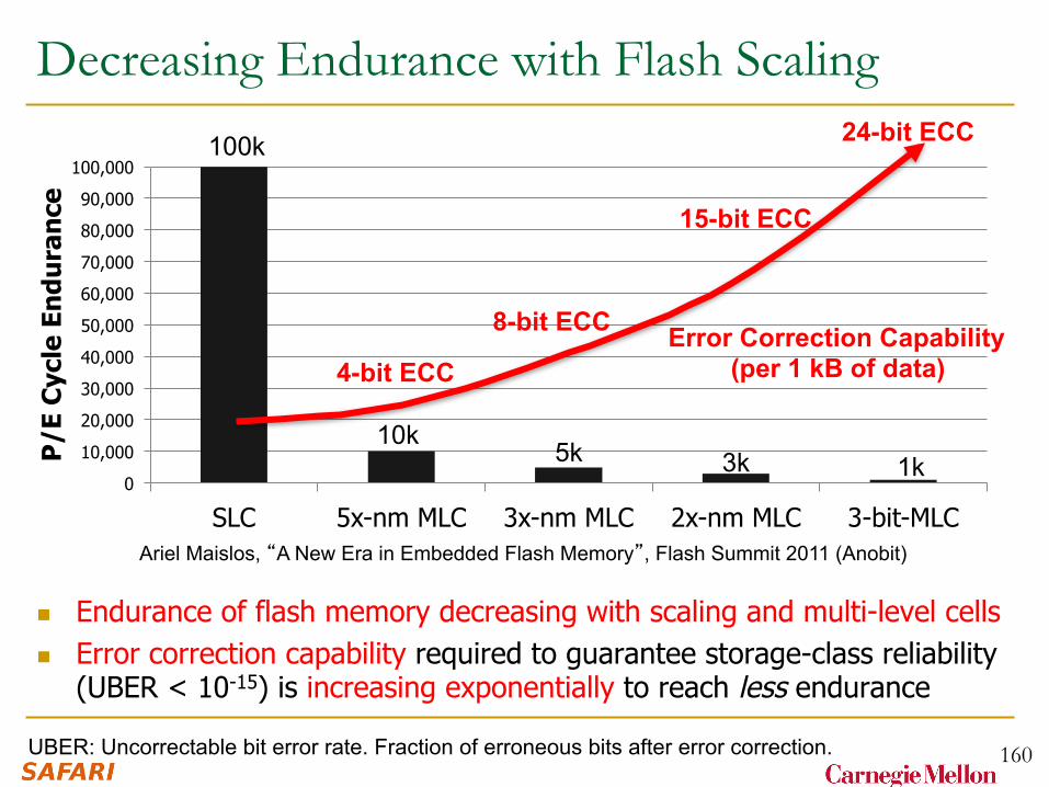
UBER: Uncorrectable bit error rate. Fraction of erroneous bits after error correction.
Decreasing Endurance with Flash Scaling
n Endurance of flash memory decreasing with scaling and multi-level cells n Error correction capability required to guarantee storage-class reliability
(UBER < 10-15) is increasing exponentially to reach less endurance
160
Ariel Maislos, “A New Era in Embedded Flash Memory”, Flash Summit 2011 (Anobit)
Error Types and Testing Methodology n Erase errors
q Count the number of cells that fail to be erased to “11” state
n Program interference errors q Compare the data immediately after page programming and the data
after the whole block being programmed
n Read errors q Continuously read a given block and compare the data between
consecutive read sequences
n Retention errors q Compare the data read after an amount of time to data written
n Characterize short term retention errors under room temperature n Characterize long term retention errors by baking in the oven
under 125℃
retention errors
n Raw bit error rate increases exponentially with P/E cycles n Retention errors are dominant (>99% for 1-year ret. time) n Retention errors increase with retention time requirement
Observations: Flash Error Analysis
166
P/E Cycles
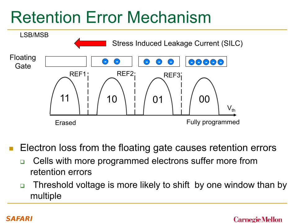
Retention Error Mechanism LSB/MSB
n Electron loss from the floating gate causes retention errors q Cells with more programmed electrons suffer more from
retention errors q Threshold voltage is more likely to shift by one window than by
multiple
11 10 01 00 Vth
REF1 REF2 REF3
Erased Fully programmed
Stress Induced Leakage Current (SILC)
Floating Gate
Retention Error Value Dependency
00 à01 01 à10
n Cells with more programmed electrons tend to suffer more from retention noise (i.e. 00 and 01)
More Details on Flash Error Analysis
n Yu Cai, Erich F. Haratsch, Onur Mutlu, and Ken Mai, "Error Patterns in MLC NAND Flash Memory: Measurement, Characterization, and Analysis" Proceedings of the Design, Automation, and Test in Europe Conference (DATE), Dresden, Germany, March 2012. Slides (ppt)
169
Threshold Voltage Distribution Shifts
As P/E cycles increase ... n Distribution shifts to the right n Distribution becomes wider
P1 State P2 State P3 State
More Detail
n Yu Cai, Erich F. Haratsch, Onur Mutlu, and Ken Mai, "Threshold Voltage Distribution in MLC NAND Flash Memory: Characterization, Analysis and Modeling" Proceedings of the Design, Automation, and Test in Europe Conference (DATE), Grenoble, France, March 2013. Slides (ppt)
171
Flash Correct-and-Refresh
Retention-Aware Error Management for Increased Flash Memory Lifetime
Yu Cai1 Gulay Yalcin2 Onur Mutlu1 Erich F. Haratsch3 Adrian Cristal2 Osman S. Unsal2 Ken Mai1
1 Carnegie Mellon University 2 Barcelona Supercomputing Center 3 LSI Corporation
Executive Summary n NAND flash memory has low endurance: a flash cell dies after 3k P/E
cycles vs. 50k desired à Major scaling challenge for flash memory n Flash error rate increases exponentially over flash lifetime n Problem: Stronger error correction codes (ECC) are ineffective and
undesirable for improving flash lifetime due to q diminishing returns on lifetime with increased correction strength q prohibitively high power, area, latency overheads
n Our Goal: Develop techniques to tolerate high error rates w/o strong ECC n Observation: Retention errors are the dominant errors in MLC NAND flash
q flash cell loses charge over time; retention errors increase as cell gets worn out n Solution: Flash Correct-and-Refresh (FCR)
q Periodically read, correct, and reprogram (in place) or remap each flash page before it accumulates more errors than can be corrected by simple ECC
q Adapt “refresh” rate to the severity of retention errors (i.e., # of P/E cycles)
n Results: FCR improves flash memory lifetime by 46X with no hardware changes and low energy overhead; outperforms strong ECCs
173
Outline n Executive Summary n The Problem: Limited Flash Memory Endurance/Lifetime n Error and ECC Analysis for Flash Memory n Flash Correct and Refresh Techniques (FCR) n Evaluation n Conclusions
174
Problem: Limited Endurance of Flash Memory n NAND flash has limited endurance
q A cell can tolerate a small number of Program/Erase (P/E) cycles q 3x-nm flash with 2 bits/cell à 3K P/E cycles
n Enterprise data storage requirements demand very high endurance q >50K P/E cycles (10 full disk writes per day for 3-5 years)
n Continued process scaling and more bits per cell will reduce flash endurance
n One potential solution: stronger error correction codes (ECC) q Stronger ECC not effective enough and inefficient
175
UBER: Uncorrectable bit error rate. Fraction of erroneous bits after error correction.
Decreasing Endurance with Flash Scaling
n Endurance of flash memory decreasing with scaling and multi-level cells n Error correction capability required to guarantee storage-class reliability
(UBER < 10-15) is increasing exponentially to reach less endurance
176
Ariel Maislos, “A New Era in Embedded Flash Memory”, Flash Summit 2011 (Anobit)
0
10,000
20,000
30,000
40,000
50,000
60,000
70,000
80,000
90,000
100,000
SLC 5x-nm MLC 3x-nm MLC 2x-nm MLC 3-bit-MLC
P/E
Cyc
le E
ndur
ance
100k
10k 5k 3k 1k
4-bit ECC
8-bit ECC
15-bit ECC
24-bit ECC
Error Correction Capability (per 1 kB of data)
The Problem with Stronger Error Correction
n Stronger ECC detects and corrects more raw bit errors à increases P/E cycles endured
n Two shortcomings of stronger ECC: 1. High implementation complexity à Power and area overheads increase super-linearly, but
correction capability increases sub-linearly with ECC strength
2. Diminishing returns on flash lifetime improvement à Raw bit error rate increases exponentially with P/E cycles, but
correction capability increases sub-linearly with ECC strength
177
Outline n Executive Summary n The Problem: Limited Flash Memory Endurance/Lifetime n Error and ECC Analysis for Flash Memory n Flash Correct and Refresh Techniques (FCR) n Evaluation n Conclusions
178
Methodology: Error and ECC Analysis n Characterized errors and error rates of 3x-nm MLC NAND
flash using an experimental FPGA-based flash platform q Cai et al., “Error Patterns in MLC NAND Flash Memory:
Measurement, Characterization, and Analysis,” DATE 2012.
n Quantified Raw Bit Error Rate (RBER) at a given P/E cycle q Raw Bit Error Rate: Fraction of erroneous bits without any correction
n Quantified error correction capability (and area and power consumption) of various BCH-code implementations q Identified how much RBER each code can tolerate
à how many P/E cycles (flash lifetime) each code can sustain
179
NAND Flash Error Types
n Four types of errors [Cai+, DATE 2012]
n Caused by common flash operations q Read errors q Erase errors q Program (interference) errors
n Caused by flash cell losing charge over time q Retention errors
n Whether an error happens depends on required retention time n Especially problematic in MLC flash because voltage threshold
window to determine stored value is smaller
180
retention errors
n Raw bit error rate increases exponentially with P/E cycles n Retention errors are dominant (>99% for 1-year ret. time) n Retention errors increase with retention time requirement
Observations: Flash Error Analysis
181
P/E Cycles
Methodology: Error and ECC Analysis n Characterized errors and error rates of 3x-nm MLC NAND
flash using an experimental FPGA-based flash platform q Cai et al., “Error Patterns in MLC NAND Flash Memory:
Measurement, Characterization, and Analysis,” DATE 2012.
n Quantified Raw Bit Error Rate (RBER) at a given P/E cycle q Raw Bit Error Rate: Fraction of erroneous bits without any correction
n Quantified error correction capability (and area and power consumption) of various BCH-code implementations q Identified how much RBER each code can tolerate
à how many P/E cycles (flash lifetime) each code can sustain
182
ECC Strength Analysis n Examined characteristics of various-strength BCH codes
with the following criteria q Storage efficiency: >89% coding rate (user data/total storage) q Reliability: <10-15 uncorrectable bit error rate q Code length: segment of one flash page (e.g., 4kB)
Power and area overheads increase super-‐linearly
n Lifetime improvement comparison of various BCH codes
Resulting Flash Lifetime with Strong ECC
184
0
2000
4000
6000
8000
10000
12000
14000
512b-BCH 1k-BCH 2k-BCH 4k-BCH 8k-BCH 32k-BCH
P/E
Cyc
le E
ndur
ance
4X Lifetime Improvement
71X Power Consumption 85X Area Consumption
Strong ECC is very inefficient at improving life,me
Our Goal
Develop new techniques to improve flash lifetime without relying on stronger ECC
185
Outline n Executive Summary n The Problem: Limited Flash Memory Endurance/Lifetime n Error and ECC Analysis for Flash Memory n Flash Correct and Refresh Techniques (FCR) n Evaluation n Conclusions
186
Flash Correct-and-Refresh (FCR) n Key Observations:
q Retention errors are the dominant source of errors in flash memory [Cai+ DATE 2012][Tanakamaru+ ISSCC 2011]
à limit flash lifetime as they increase over time q Retention errors can be corrected by “refreshing” each flash
page periodically
n Key Idea: q Periodically read each flash page, q Correct its errors using “weak” ECC, and q Either remap it to a new physical page or reprogram it in-place, q Before the page accumulates more errors than ECC-correctable q Optimization: Adapt refresh rate to endured P/E cycles
187
FCR Intuition
188
Errors with No refresh
ProgramPage ×
After time T × × ×
After time 2T × × × × ×
After time 3T × × × × × × ×
×
× × ×
× × ×
× × ×
×
×
Errors with Periodic refresh
×
× Retention Error × Program Error
FCR: Two Key Questions
n How to refresh? q Remap a page to another one q Reprogram a page (in-place) q Hybrid of remap and reprogram
n When to refresh? q Fixed period q Adapt the period to retention error severity
189
Outline n Executive Summary n The Problem: Limited Flash Memory Endurance/Lifetime n Error and ECC Analysis for Flash Memory n Flash Correct and Refresh Techniques (FCR)
1. Remapping based FCR 2. Hybrid Reprogramming and Remapping based FCR 3. Adaptive-Rate FCR
n Evaluation n Conclusions
190
Outline n Executive Summary n The Problem: Limited Flash Memory Endurance/Lifetime n Error and ECC Analysis for Flash Memory n Flash Correct and Refresh Techniques (FCR)
1. Remapping based FCR 2. Hybrid Reprogramming and Remapping based FCR 3. Adaptive-Rate FCR
n Evaluation n Conclusions
191
Remapping Based FCR
n Idea: Periodically remap each page to a different physical page (after correcting errors)
q Also [Pan et al., HPCA 2012]
q FTL already has support for changing logical à physical flash block/page mappings q Deallocated block is erased by garbage collector
n Problem: Causes additional erase operations à more wearout q Bad for read-intensive workloads (few erases really needed) q Lifetime degrades for such workloads (see paper)
192
Outline n Executive Summary n The Problem: Limited Flash Memory Endurance/Lifetime n Error and ECC Analysis for Flash Memory n Flash Correct and Refresh Techniques (FCR)
1. Remapping based FCR 2. Hybrid Reprogramming and Remapping based FCR 3. Adaptive-Rate FCR
n Evaluation n Conclusions
193
In-Place Reprogramming Based FCR
n Idea: Periodically reprogram (in-place) each physical page (after correcting errors)
q Flash programming techniques (ISPP) can correct retention errors in-place by recharging flash cells
n Problem: Program errors accumulate on the same page à may not be correctable by ECC after some time
194
Reprogram corrected data
n Pro: No remapping needed à no additional erase operations n Con: Increases the occurrence of program errors
In-Place Reprogramming of Flash Cells
195
Retention errors are caused by cell voltage shifting to the left
ISPP moves cell voltage to the right; fixes retention errors
Floating Gate Voltage Distribution
for each Stored Value
Floating Gate
Program Errors in Flash Memory
n When a cell is being programmed, voltage level of a neighboring cell changes (unintentionally) due to parasitic capacitance coupling
à can change the data value stored
n Also called program interference error
n Program interference causes neighboring cell voltage to shift to the right
196
Problem with In-Place Reprogramming
197
11 10 01 00 VT
REF1 REF2 REF3
Floating Gate
Additional Electrons Injected
… … 11 01 00 10 11 00 00 Original data to be programmed
… … 10 01 00 10 11 00 00 Program errors after initial programming
… … Retention errors after some time 10 10 00 11 11 01 01
n Idea: q Monitor the count of right-shift errors (after error correction) q If count < threshold, in-place reprogram the page q Else, remap the page to a new page
n Observation: q Program errors much less frequent than retention errors à
Remapping happens only infrequently
n Benefit: q Hybrid FCR greatly reduces erase operations due to remapping
198
Outline n Executive Summary n The Problem: Limited Flash Memory Endurance/Lifetime n Error and ECC Analysis for Flash Memory n Flash Correct and Refresh Techniques (FCR)
1. Remapping based FCR 2. Hybrid Reprogramming and Remapping based FCR 3. Adaptive-Rate FCR
n Evaluation n Conclusions
199
Adaptive-Rate FCR
n Observation: q Retention error rate strongly depends on the P/E cycles a flash
page endured so far q No need to refresh frequently (at all) early in flash lifetime
n Idea: q Adapt the refresh rate to the P/E cycles endured by each page q Increase refresh rate gradually with increasing P/E cycles
n Benefits: q Reduces overhead of refresh operations q Can use existing FTL mechanisms that keep track of P/E cycles
200
Adaptive-Rate FCR (Example)
201
Acceptable raw BER for 512b-BCH
3-year FCR
3-month FCR
3-week FCR
3-day FCR
P/E Cycles
Select refresh frequency such that error rate is below acceptable rate
Outline n Executive Summary n The Problem: Limited Flash Memory Endurance/Lifetime n Error and ECC Analysis for Flash Memory n Flash Correct and Refresh Techniques (FCR)
1. Remapping based FCR 2. Hybrid Reprogramming and Remapping based FCR 3. Adaptive-Rate FCR
n Evaluation n Conclusions
202
FCR: Other Considerations
n Implementation cost q No hardware changes q FTL software/firmware needs modification
n Response time impact q FCR not as frequent as DRAM refresh; low impact
n Adaptation to variations in retention error rate q Adapt refresh rate based on, e.g., temperature [Liu+ ISCA 2012]
n FCR requires power q Enterprise storage systems typically powered on
203
Outline n Executive Summary n The Problem: Limited Flash Memory Endurance/Lifetime n Error and ECC Analysis for Flash Memory n Flash Correct and Refresh Techniques (FCR) n Evaluation n Conclusions
204
Evaluation Methodology n Experimental flash platform to obtain error rates at
different P/E cycles [Cai+ DATE 2012]
n Simulation framework to obtain P/E cycles of real workloads: DiskSim with SSD extensions
Base (No-‐Refresh) Remapping-‐Based FCR Hybrid FCR Adap,ve FCR
46x
Adap?ve-‐rate FCR provides the highest life?me Life?me of FCR much higher than life?me of stronger ECC
4x
Lifetime Evaluation Takeaways n Significant average lifetime improvement over no refresh
q Adaptive-rate FCR: 46X q Hybrid reprogramming/remapping based FCR: 31X q Remapping based FCR: 9X
n FCR lifetime improvement larger than that of stronger ECC q 46X vs. 4X with 32-kbit ECC (over 512-bit ECC) q FCR is less complex and less costly than stronger ECC
n Lifetime on all workloads improves with Hybrid FCR q Remapping based FCR can degrade lifetime on read-heavy WL q Lifetime improvement highest in write-heavy workloads
208
Energy Overhead
n Adaptive-rate refresh: <1.8% energy increase until daily
refresh is triggered
209
0%
2%
4%
6%
8%
10%
1 Year 3 Months 3 Weeks 3 Days 1 Day
Ener
gy O
verh
ead
Remapping-based Refresh Hybrid Refresh
7.8%
5.5%
2.6% 1.8%
0.4% 0.3%
Refresh Interval
Overhead of Additional Erases
n Additional erases happen due to remapping of pages
n Low (2%-20%) for write intensive workloads n High (up to 10X) for read-intensive workloads
n Improved P/E cycle lifetime of all workloads largely outweighs the additional P/E cycles due to remapping
210
More Results in the Paper
n Detailed workload analysis
n Effect of refresh rate
211
Outline n Executive Summary n The Problem: Limited Flash Memory Endurance/Lifetime n Error and ECC Analysis for Flash Memory n Flash Correct and Refresh Techniques (FCR) n Evaluation n Conclusions
212
Conclusion n NAND flash memory lifetime is limited due to uncorrectable
errors, which increase over lifetime (P/E cycles)
n Observation: Dominant source of errors in flash memory is retention errors à retention error rate limits lifetime
n Flash Correct-and-Refresh (FCR) techniques reduce retention error rate to improve flash lifetime q Periodically read, correct, and remap or reprogram each page
before it accumulates more errors than can be corrected q Adapt refresh period to the severity of errors
n FCR improves flash lifetime by 46X at no hardware cost q More effective and efficient than stronger ECC q Can enable better flash memory scaling
213
Flash Correct-and-Refresh
Retention-Aware Error Management for Increased Flash Memory Lifetime
Yu Cai1 Gulay Yalcin2 Onur Mutlu1 Erich F. Haratsch3 Adrian Cristal2 Osman S. Unsal2 Ken Mai1
1 Carnegie Mellon University 2 Barcelona Supercomputing Center 3 LSI Corporation