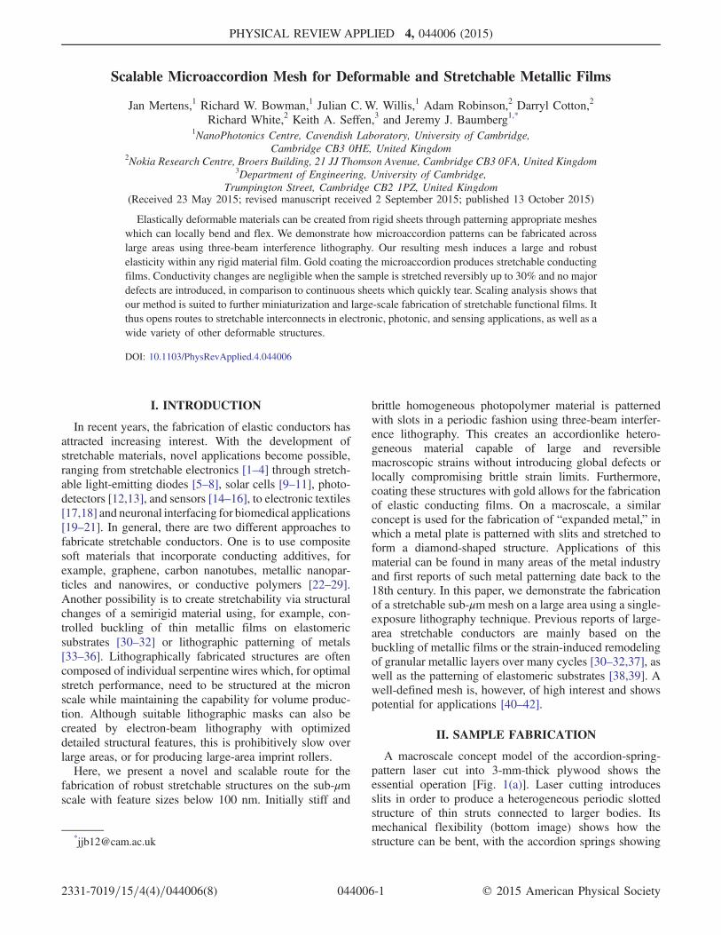
Scalable Microaccordion Mesh for Deformable and Stretchable Metallic Films
Jan Mertens,1 Richard W. Bowman,1 Julian C.W. Willis,1 Adam Robinson,2 Darryl Cotton,2
Richard White,2 Keith A. Seffen,3 and Jeremy J. Baumberg1,*1NanoPhotonics Centre, Cavendish Laboratory, University of Cambridge,
Cambridge CB3 0HE, United Kingdom2Nokia Research Centre, Broers Building, 21 JJ Thomson Avenue, Cambridge CB3 0FA, United Kingdom
3Department of Engineering, University of Cambridge,Trumpington Street, Cambridge CB2 1PZ, United Kingdom
(Received 23 May 2015; revised manuscript received 2 September 2015; published 13 October 2015)
Elastically deformable materials can be created from rigid sheets through patterning appropriate mesheswhich can locally bend and flex. We demonstrate how microaccordion patterns can be fabricated acrosslarge areas using three-beam interference lithography. Our resulting mesh induces a large and robustelasticity within any rigid material film. Gold coating the microaccordion produces stretchable conductingfilms. Conductivity changes are negligible when the sample is stretched reversibly up to 30% and no majordefects are introduced, in comparison to continuous sheets which quickly tear. Scaling analysis shows thatour method is suited to further miniaturization and large-scale fabrication of stretchable functional films. Itthus opens routes to stretchable interconnects in electronic, photonic, and sensing applications, as well as awide variety of other deformable structures.
DOI: 10.1103/PhysRevApplied.4.044006
I. INTRODUCTION
In recent years, the fabrication of elastic conductors hasattracted increasing interest. With the development ofstretchable materials, novel applications become possible,ranging from stretchable electronics [1–4] through stretch-able light-emitting diodes [5–8], solar cells [9–11], photo-detectors [12,13], and sensors [14–16], to electronic textiles[17,18] and neuronal interfacing for biomedical applications[19–21]. In general, there are two different approaches tofabricate stretchable conductors. One is to use compositesoft materials that incorporate conducting additives, forexample, graphene, carbon nanotubes, metallic nanopar-ticles and nanowires, or conductive polymers [22–29].Another possibility is to create stretchability via structuralchanges of a semirigid material using, for example, con-trolled buckling of thin metallic films on elastomericsubstrates [30–32] or lithographic patterning of metals[33–36]. Lithographically fabricated structures are oftencomposed of individual serpentine wires which, for optimalstretch performance, need to be structured at the micronscale while maintaining the capability for volume produc-tion. Although suitable lithographic masks can also becreated by electron-beam lithography with optimizeddetailed structural features, this is prohibitively slow overlarge areas, or for producing large-area imprint rollers.Here, we present a novel and scalable route for the
fabrication of robust stretchable structures on the sub-μmscale with feature sizes below 100 nm. Initially stiff and
brittle homogeneous photopolymer material is patternedwith slots in a periodic fashion using three-beam interfer-ence lithography. This creates an accordionlike hetero-geneous material capable of large and reversiblemacroscopic strains without introducing global defects orlocally compromising brittle strain limits. Furthermore,coating these structures with gold allows for the fabricationof elastic conducting films. On a macroscale, a similarconcept is used for the fabrication of “expanded metal,” inwhich a metal plate is patterned with slits and stretched toform a diamond-shaped structure. Applications of thismaterial can be found in many areas of the metal industryand first reports of such metal patterning date back to the18th century. In this paper, we demonstrate the fabricationof a stretchable sub-μmmesh on a large area using a single-exposure lithography technique. Previous reports of large-area stretchable conductors are mainly based on thebuckling of metallic films or the strain-induced remodelingof granular metallic layers over many cycles [30–32,37], aswell as the patterning of elastomeric substrates [38,39]. Awell-defined mesh is, however, of high interest and showspotential for applications [40–42].
II. SAMPLE FABRICATION
A macroscale concept model of the accordion-spring-pattern laser cut into 3-mm-thick plywood shows theessential operation [Fig. 1(a)]. Laser cutting introducesslits in order to produce a heterogeneous periodic slottedstructure of thin struts connected to larger bodies. Itsmechanical flexibility (bottom image) shows how thestructure can be bent, with the accordion springs showing*[email protected]
compressibility and stretchability at the same time due tothe local bending and twisting of the struts. The inter-connecting bodies do not deform, but displace rigidly withthe strut ends.On the micrometer scale, samples are fabricated in
photoresist using a highly specific configuration ofthree-beam interference lithography (Appendixes 1, 2).Three 405-nm laser beams of equal intensity illuminatean 1.8-μm-thick photoresist (AZ 5214E) film that is spincoated on a flexible polydimethylsiloxane (PDMS) sub-strate [Fig. 1(b)]. The inset depicts the required angles ofthe incident laser beams referenced to the layer normal (z).Reports in the literature study the laser-beam arrangementnecessary to obtain square or hexagonal lattices in a single-exposure step [43–46]. Instead here, two beams irradiatethe photoresist in the y-z plane with an angle of 20°between them, creating an interference grating in thesample plane. A third beam illuminates the sample inthe x-z plane at an angle of 0.5° to the surface normal,perturbing this interference grating. This perturbationcreates an accordion-spring structure, seen in the bottomunderlay of Fig. 1(b), which shows the calculated inter-ference pattern with white (black) areas as high (low)illumination intensity. By changing the relative angles ofgrating and perturbing beams, the structures can be scaleddown to the deep submicron domain and a wide variety ofdifferent structures can be generated (SupplementalMaterial, Sec. A [47]). For exploring the conductiveproperties of the mesh, the accordions are evaporativelycoated with 40 nm of Au.
III. RESULTS
A. Mechanical characterization—Experimentaland theoretical
The accordion structures are uniform over centimeterlength scales. A typical scanning electron microscopy(SEM) segment is shown in Fig. 1(c). The white horizontalwavy lines in the SEM image mark the areas of maximumperturbation in the interference grating, seen more clearly inthe highermagnification of the positive photoresist structure[Fig. 1(d)]. The structure gains its stretchability from thedeep slits. The slope of the wall profile at the connectingstruts is set by the absorption of the photoresist, while theaspect ratio of the slits [slit lengthL to widthW, Fig. 2(e)] isdefined by the absorption of the resist, the resist thickness,and the angle between the perturbing laser beam and thesurface normal (Supplemental Material, Sec. A) [47]. All ofthese can be controlled by varying the resist parameters, andfor the situation here the slits have an aspect ratio of ∼10.This aspect ratio can be further increased by using thinnerphotoresist or illuminating for longer, but it is limited as thestructure becomesmore fragile leading to larger defect areas(Supplemental Material, Sec. B [47]). Struts in the inter-penetration area are thin at the top (width ∼100 nm) andwiden towards the PDMS substrate following the absorptionprofile of the photoresist.The accordion-spring structures are uniaxially stretched
perpendicular to the narrow slits [Fig. 2(a), orange arrows]with a computer-controlled stage (Appendix 3). An SEMimage (taken at 30° viewing) of the relaxedAu-coated sample
FIG. 1 (a) Concept of the accordion-spring structure made from 3-mm-thick plywood, showing flexibility. (b) Schematic ofinterference lithography for fabricating the structure. The inset depicts angles of incident laser beams with respect to surface normal. (c),(d) SEM pictures showing (c) the high uniformity and (d) a close-up of the structure on a PDMS substrate.
FIG. 2. (a)–(d) Accordion springstructure in relaxed state (left col-umn) and stretched state (rightcolumn), shown in schematic (a),(c) and SEM (b),(d); orange arrowsdepict the stretchdirection. (e)Sim-ulation of the local strain at the topsurface when the full structure isextended by 20%. (f) Schematiccross section of the stretched struc-ture illustrating the Au butterflyeffect when stretched.
JAN MERTENS et al. PHYS. REV. APPLIED 4, 044006 (2015)
044006-2
after repeated stretching cycles is shown in Fig. 2(b). Smallcracks in the Au coating are visible at the thin connectingstruts which emerge only after prolonged stretch cycling.Stretching leads to bending of the relatively straight struts intogentle S curves and widening of the slits between theinterconnected bodies, producing a macroscopic strain ofthe accordion structure [Figs. 2(c) and 2(d)]. Twisting ofstruts occurs along two axes, in-plane deformations initiallyand then out of plane as discussed below. To gain insight intothe degree of local strain within the struts, a finite-elementsimulation of the mechanical properties of the full structure,i.e., of the patterned photoresist including the PDMS sub-strate, is performed (Supplemental Material, Sec. D [47]).Here, however,we focus on the simulation results of the strainat the top surface since cracks in the gold coatings follow thisstrain distribution. A discussion of strain in and at the bottomof the structure is given in the Supplemental Material [47].When the accordion-spring structure is, for example,stretched by 20%, the local strains are highly concentratedalong the connecting struts [Fig. 2(e)], where the maximummaterial strain is approximately3%.Even a strainof 3% in theexperiment would likely lead to an electrical failure of thedevice, which is not observed. Therefore, additional stress-reduction processesmust take placewhich are not included inthemodel.Oneof these processes is the planar deformation ofthe struts that induces crack formation of the overlying goldcoating seen in the SEMs. The strain diffuses rapidly into themain bodies which are not strained across their bulk,accounting for the robustness and elastic stretching of thedesign. As well as deforming in plane, the struts undergoorthogonal straining in the out-of-plane direction, resulting ina surface displacement. These strains follow from the rigidboundary conditions between the overall structure and theunderlying PDMS substrate, which is confirmed by finite-element simulations (Supplemental Material, Sec. D) [47].This indicates that the surface displacement causes the Aucoating to delaminate selectively away from the sidewalls ofthe main ribs, which can be seen directly in the center of thespring structure [Fig. 2(d)]. The delamination is visible assubmicron Au wings that bend upwards when the sample isstretched, illustrated schematically in cross section inFig. 2(f). This Au-film buckling is reversible upon relaxingthe strain, giving rise to three-dimensional dynamical recon-figuration (like a butterfly wing) induced from the initial 2Dpatterning, while no damage is introduced to the photoresistribbons directly underneath. The Au-wing delamination is anadditionalprocess that reducesstress in theAulayer tokeep thefilm intact. No Au lift-off from the ribbons is observed whenstretching the mesh, which suggests good structural strainrelief and strong adhesion between gold film and photoresist.
B. Optical characterization
The planar deformation is further studied by opticalcharacterization of the Au-coated microaccordion sheets.Samples are mounted in a computer-controlled translation
stage inside a microscope, enabling optical micrographs tobe recorded while stretching the samples horizontally[Fig. 3(a)]. Darker regions show the slits, while thebright-golden areas correspond to the Au-coated photo-resist. Quantitative characterization of these flexible dif-fraction gratings uses blue laser light incident through themicroscope onto the sample giving diffracted lightobserved in the back focal plane of the microscopeobjective using a Bertrand lens (Appendix 4). The dif-fraction pattern of white light in transmission is shown inthe inset, showing the first diffraction orders and allowingcalibration of the structure periodicity via the diffractionequation. The red arrows indicate a span of ten accordionsprings revealing the slits opening up as a strain of 10% isapplied. The structure responds linearly with a 10%increase in the periodicity confirmed by the diffractionmeasurements [Fig. 3(b)]. The linearly increasing perio-dicity with strain confirms that the patterned photoresistremains fully attached to the underlying PDMS substratewithout delamination.
C. Electronic characterization
The Au-coated microaccordions are contacted with twomicromanipulator probes for conductive measurements toreveal howsuch accordion-spring films canbeused as elasticconductors (Appendix 5). Optical images of a contactedsample in relaxed and stretched states are shown in the insetsof Fig. 4(a). In each step, the probes are lifted up before thesample is stretched and afterwards placed down on the samerib to ensure conductivitymeasurements over a fixednumberof accordion springs. Samples stretched up to 30% show thatthe resistance is almost constant over the entire range.Fluctuations in the resistance are mainly due to variationsin contact resistance with repeated probe-tip landings on thesame ribs. While four-point electrical measurements arecurrently not feasible in such densemeshes, these results still
FIG. 3 (a) Microscope images of microaccordion in the relaxed(top) and stretched (bottom) state. Red arrows mark the width often accordion springs showing 10% stretch. (b) Correspondingperiodicity measured from white-light diffraction (inset) whilestretching.
demonstrate the lack of any strong increase in sheet resis-tance.While stretching of the samples beyond 30% results inrupture of the PDMS substrate, no failure of the Au-coatedaccordion pattern is observed. Small microcracks formedwhen stretching the sample or local defects from thelithography process do not significantly influence theconductivity. Stretching and relaxing of samples is fullyreversible and even when cycled more than 100 times nofailure of the device is discerned. Results of a durability testare shown in Fig. 4(b). A sample is stretched by 30% in eachcycle and the resistance ismeasured in the stretched state. Forthe first 20 stretch cycles, an unexpected fast drop inresistance is observed. This decrease in resistance continuesto develop over the next 80 cycles showing that the micro-accordion sheet does not lose its conductivity, but improveswith cycling.The drop in resistance is likely explainedby theformation of complex networks of microcracks in thestretched and bent metal coatings. Such crack networksare observed in the SEM images of Figs. 2(b) and 2(d) and
widely reported in the literature [31]. Cracks reduce in sizeover many cycles, allowing the metal to better wrap aroundstrut edges and thus reducing the resistance of the linkerstruts which form local bottlenecks for electrical transport.Furthermore, such cracks reduce the residual strain in thegold coating of themesh pattern,which can additionally leadto a reduction of the Au resistivity after multiple stretchcycles.
IV. DISCUSSION
The advantage of an interference lithographic route tosuch deformable microaccordion networks is the strongprospect for scalable films, using it either directly, or byexploiting it to create masters for embossing in a roll-to-rollcontinuous process. Structure sizes down below 100 nm arepossible simply by moving to deeper UV laser processing.A simplified analytical model of the accordion mesh showsthat reducing the strut width and increasing the aspect ratioof slits results in a reduction of the force required for elasticdeformations. In this model, only deformations of theconnecting struts are assumed, following our observationsabove. Out-of-plane deformations of the mesh along thesurface normal are neglected.The considered simplified mesh is sketched in Fig. 5(a).
It is stretched along the x direction due to the application ofa uniaxial long-range stress σx. Deformation of the mesh islocalized in the junction region (blue box A). Singlejunction beams [Fig. 5(b)] are defined by a pair of equalbut oppositely curved cantilevers (blue box B) with aninitial stress-free radius of curvature R, subtending angle α.The forces acting on one-half of a junction beam aredisplayed in Fig. 5(c). This force induces an in-planedisplacement u and v as well as a bending moment M0,from the connection to the next junction beam.Deformations of the beams can be well approximated bya tip-loaded curved cantilever. The tip of this cantilever is
FIG. 4 (a) Resistance measurement of microaccordion sheetversus strain. The insets show in situ microprobes for conductingmeasurements on the accordion pattern in relaxed (top) andstretched (bottom) states. (b) Resistance versus stretch cycles ofthe Au-coated sheet.
(b)
M0
F
W
x(a)
x
x
y
(c)
F
t
F
L
u
F
v
A B
R
FIG. 5. Analytical model for estimating tensile performance of the accordion mesh. (a) Schematic layout of the mesh under uniaxiallong-range stress σx. Dimensions of a typical unit cell are W × L. (b) Enlarged blue box A showing the junction line of in-planethickness t, acted on by opposing forces F which arise from σx. The stress-free radius of curvature is R subtending α: (c) One-half of atypical junction beam, box B, behaving as a tip-loaded cantilever embedded at the opposite end. The corresponding displacements underF are u and v, and M0 is the moment reaction transferred at the connection point, along with F, to the next junction beam (not shown).
JAN MERTENS et al. PHYS. REV. APPLIED 4, 044006 (2015)
044006-4
displaced under the applied load, describing axial strainsεx; εy in the unit cell:
εx ¼4vL; εy ¼
4uW
: ð1Þ
Here, a factor of 4 is included because each unit cellconsists of four cantilever beams in the junction line. Thetip displacement δ ¼ ðν; uÞ of the cantilever is obtainedfollowing the method of virtual work for beams and frames(see Supplemental Material, Sec. C) [47]:
P�δ ¼Z
M�κds; ð2Þ
where P⋆ is the applied “virtual” load at the point of interestin the desired direction, M⋆ is the corresponding virtualbending moment, κ is the change in beam curvature when aload is applied, and ds is the beam arc-length. The bendingmoment varies along the cantilever and is hence a functionof the angle θ, of the applied force F, and of the radius ofcurvature R of the stress-free cantilever [Fig. 5(c)]:
MðθÞ ¼ FðR sin α − R sin θÞ: ð3Þ
The change in curvature depends on the Young’smodulus E of the material and the second area momentof the cross section about the bending axis I ¼ bt3=12 withthe cantilever depth b. It is obtained from the constitutiveelastic law for slender beams,
κ ¼ MðθÞ=EI: ð4Þ
Inserting Eqs. (3) and (4) into Eq. (1) and integrating withan applied virtual unit force P⋆ ¼ 1⋆ provides the beamdisplacements along the x and y directions (SupplementalMaterial, Sec. C) [47]. Since F depends on σx, an effectiveaxial modulus for the mesh can then be defined,
σxεx
∝ E
�tR
�3 WL: ð5Þ
This effective axial modulus in Eq. (5) is inverselyproportional to the aspect ratio L=W, as well as scaling withthe cube of strut thickness to the link strut curvature.Increasing the aspect ratio thus linearly decreases the forceneeded to elastically stretch the mesh. The aspect ratio canbe directly controlled via the precise angular laser beamarrangement, as shown in the Supplemental Material,Sec. A [47]. Additionally, exposure and development allowcontrol of strut thickness. This analysis shows how thefurther reduction of feature sizes will ensure that therequired operational forces can be also reduced.Aswell as films on flexible substrates, free-standing films
can be floated off. However, free-standing films are difficult
to handle and are, therefore, often not suitable for applica-tions. By combining accordion-spring motifs in differentorientations on the resist films—for instance, using a spatiallight modulator to direct different beams to different regionsof the film—omnidirectional accordion stretching can beproduced (Supplemental Material, Sec. E) [47]. Similarly,although we demonstrate only up to 30% strain so far,limited by our choice of substrate material, larger strains canbe supported by the accordion springs, with limits still to befully understood. While we use here simple Au coating ofthe patterned photoresist, the material choice can be widelyextended to many metallic and multilayer structures usinglift-off, moulding, or printing techniques (SupplementalMaterial, Sec. B) [47]. As a result, this opens up a largevariety of nanopatterned stretchable film designs that canhave optical, electronic, magnetic, and sensing functionalitybuilt in, yet be low cost and a large area.For example, complicated structures can be generated
when multiple exposures are used. The calculated interfer-ence patterns of double exposures with three beams arepresented in Fig. 6. In both cases, all three laser beams havean angle θ ¼ 10° with respect to the surface normal. In (a),the sample is rotated by α ¼ 10° after the first exposure,while a sample rotation of α ¼ 30° is used in (b). Bothconfigurations generate porous resist films that allow for acontrolled fabrication route to stretchable, spongelike thinfilms. Stretching structure (a) leads to a displacement of therepeating units accompanied by rotations of connectionsas indicated, so that conductive contacts remain intact.However, scaling up of such fabrication processes to largeareas is more complicated than for the accordion-springpattern due to the additional rotation step of the substraterelative to the illuminating beams. Therefore, the accordionmesh is chosen here for fabrication with single-exposurethree-beam interference lithography. In addition, we notethat electron-beam lithography can access additional geom-etries of such nanostructures for microscale testing, but asdiscussed above, the fabrication process cannot be applied
FIG. 6. Calculated interference patterns of more complexstructures. A double exposure is used in which the sample isrotated after the first exposure step by (a) α ¼ 10° and(b) α ¼ 30°, as indicated in the diagrams at the top.
on the large scales needed for a large-area process. Furtherwork is thus focused on optimizing pattern geometries thatare accessible, have high yield, and can be scaled tolarge areas.
V. CONCLUSION
In conclusion, we have presented an approach tofabricating stretchable microstructures by patterning photo-resist using three-beam interference lithography in aspecific orientation. Key to this approach is creating longcuts into a brittle material that can then respond throughstrut bending and twisting. The resulting accordion-springpatterns are robust, and with strongly interpenetrating slitsthey can be highly stretched. Elasticity measurements showthe film’s potential as its conductivity is maintained onstretching. Microaccordion patterning thus generates aroute for the fabrication of elastic metals. Further minia-turization and functionalization of the structure can beachieved by changing the illuminating geometry in thelithography, and adapting to incorporate materials. Ouranalysis shows that the elastic properties improve as thesepatterns are miniaturized, giving strong motivation for suchnanostructuring. Our approach to using interference lithog-raphy enables large-scale fabrication of lithographicallydefined stretchable metallic films and thus routes tostretchable interconnects and pads in electronics, photon-ics, and sensing applications.
ACKNOWLEDGMENTS
We are grateful for funding from the CambridgeNanoDTC, ERC LINASS 320503 and U.K. EPSRCGrants No. EP/G060649/1, No. EP/G037221/1, No. EP/L027151/1, and No. EP/L015978/1, as well as NokiaResearch. R.W. B. thanks Queens’ College Cambridgefor financial support. J. M. acknowledges support fromthe Winton Programme for the Physics of Sustainability.
APPENDIX: EXPERIMENTAL DETAILS
1. Fabrication of PDMS substrates
PDMS (Sylgard 184 Elastomer Kit, Dow Corning) isprepared using a 10:1 degassed mix of base and curingagent that is cast in glass dishes with cleaned 1.5 × 1.5 cm2
glass substrates. These substrates are covered by 1 mm ofPDMS and baked in an oven for 4 h at 70 °C. The curedPDMS is cut free from the glass dish with a 3-mm borderaround the glass substrates, which are subsequentlyremoved. The support border is glued on a larger glasssubstrate to allow simple handling without contact betweenglass and PDMS.
2. Interference lithography
The PDMS substrates are cleaned with acetone and IPAbefore photoresist (AZ 5214E) is spin coated on the dried
substrates with 8000 rpm for 30 s to gain a film with athickness of 1.8 μm. A soft baking step with 115 °C for 60 sensures that remaining solvent is removed. The illumina-tion of a circular area with a diameter of 1.4 cm isperformed with three 405-nm laser beams and a totalintensity of 12 mW for 14 s. The sample remains in adeveloping bath with a 1:4 solution of AZ 351B developerand deionized water for 50 s. Electron-beam evaporation isused to coat the developed samples with 40 nm of Au.
3. Stretch measurements
Stretch measurements are performed on a computer-controlled linear translation stage mounted in a microscope.For the optical characterization, an adapted Olympus BX51microscope in bright-field configuration is used. Thestructure morphology is examined in a scanning electronmicroscope equipped with an extensometer.
4. Diffraction measurements
White light from an incandescent source or a laser with awavelength of 448 nm (Coherent Cube) illuminated thesample with parallel light rays through the microscopeobjective. Diffracted light is collected and imaged in theback focal plane of the objective using a Bertrand lens.
5. Electric measurements
Resistance measurements are performed by contactingthe samples with two microprobes (20-μm gold wires)attached to micromanipulators (Kleindiek Nanotechnik) toensure precise positioning of the probes. A voltage of150 μV (Keithley 2635 A) is applied to the sample and theresistance is measured.
6. Simulations
Strain simulations are performed using commercialsoftware (COMSOL). The photoresist AZ 5124E is modeledas a linear elastic material with a Young’s modulus of 7 GPa[48]; PDMS is modeled as a hyperelastic material usingthe Mooney-Rivlin fit with parameters E ¼ 1.23 MPa,C1 ¼ 0.205 MPa, C2 ¼ 0 MPa (corresponding to a 24-hour cure at 60 °C) [49]. Symmetric boundary conditionsare applied at each vertical face. A displacement boundarycondition is applied to each end of the PDMS/AZ structurein order to provide a total applied strain of 20%. Thesimulation included nonlinear geometrical effects.Postprocessing strain slices are recorded at the base andthe surface of the AZ structure.
[1] M. Park, J. Im, M. Shin, Y. Min, J. Park, H. Cho, S. Park,M.-B. Shim, S. Jeon, D.-Y. Chung, J. Bae, J. Park, U. Jeong,and K. Kim, Highly stretchable electric circuits from acomposite material of silver nanoparticles and elastomericfibres, Nat. Nanotechnol. 7, 803 (2012).
JAN MERTENS et al. PHYS. REV. APPLIED 4, 044006 (2015)
[2] M. Kaltenbrunner, T. Sekitani, J. Reeder, T. Yokota,K. Kuribara, T. Tokuhara, M. Drack, R. Schwödiauer, I.Graz, S. Bauer-Gogonea, S. Bauer, and T. Someya, An ultra-lightweight design for imperceptible plastic electronics,Nature (London) 499, 458 (2013).
[3] A. Chortos, J. Lim, J. W. F. To, M. Vosgueritchian,T. J. Dusseault, T.-H. Kim, S. Hwang, and Z. Bao, Highlystretchable transistors using a microcracked organic semi-conductor, Adv. Mater. 26, 4253 (2014).
[4] Y.-C. Lai, Y.-C. Huang, T.-Y. Lin, Y.-X. Wang, C.-Y. Chang,Y. Li, T.-Y. Lin, B.-W. Ye, Y.-P. Hsieh, W.-F. Su, Y.-J. Yang,and Y.-F. Chen, Stretchable organic memory: Towardlearnable and digitized stretchable electronic applications,NPG Asia Mater. 6, e87 (2014).
[5] T. Sekitani, H. Nakajima, H. Maeda, T. Fukushima, T. Aida,K. Hata, and T. Someya, Stretchable active-matrix organiclight-emitting diode display using printable elastic conduc-tors, Nat. Mater. 8, 494 (2009).
[6] R.-H. Kim, D.-H. Kim, J. Xiao, B. H. Kim, S.-I. Park, B.Panilaitis, R. Ghaffari, J. Yao, M. Li, Z. Liu, V. Malyarchuk,D. G. Kim, A.-P. Le, R. G. Nuzzo, D. L. Kaplan, F. G.Omenetto, Y. Huang, Z. Kang, and J. A. Rogers, WaterproofAlInGaP optoelectronics on stretchable substrates withapplications in biomedicine and robotics, Nat. Mater. 9,929 (2010).
[7] Z. Yu, X. Niu, Z. Liu, and Q. Pei, Intrinsically stretchablepolymer light-emitting devices using carbon nanotube-polymer composite electrodes, Adv. Mater. 23, 3989 (2011).
[8] H. L. Filiatrault, G. C. Porteous, R. S. Carmichael, G. J. E.Davidson, and T. B. Carmichael, Stretchable light-emittingelectrochemical cells using an elastomeric emissivematerial, Adv. Mater. 24, 2673 (2012).
[9] J. Lee, J. Wu, M. Shi, J. Yoon, S.-I. Park, M. Li, Z. Liu, Y.Huang, and J. A. Rogers, Stretchable GaAs photovoltaicswith designs that enable high areal coverage, Adv. Mater.23, 986 (2011).
[10] D. J. Lipomi, B. C.-K. Tee, M. Vosgueritchian, and Z. Bao,Stretchable organic solar cells, Adv. Mater. 23, 1771 (2011).
[11] M. Kaltenbrunner, M. S. White, E. D. Głowacki, T. Sekitani,T. Someya, N. S. Sariciftci, and S. Bauer, Ultrathin andlightweight organic solar cells with high flexibility, Nat.Commun. 3, 770 (2012).
[12] P. Bartu, R. Koeppe, N. Arnold, A. Neulinger, L. Fallon, andS. Bauer, Conformable large-area position-sensitive photo-detectors based on luminescence-collecting silicone wave-guides, J. Appl. Phys. 107, 123101 (2010).
[13] Y. M. Song, Y. Xie, V. Malyarchuk, J. Xiao, I. Jung, K.-J.Choi, Z. Liu, H. Park, C. Lu, R.-H. Kim, R. Li, K. B.Crozier, Y. Huang, and J. A. Rogers, Digital cameras withdesigns inspired by the arthropod eye, Nature (London) 497,95 (2013).
[14] T. Someya, Y. Kato, T. Sekitani, S. Iba, Y. Noguchi, Y.Murase, H. Kawaguchi, and T. Sakurai, Conformable,flexible, large-area networks of pressure and thermal sensorswith organic transistor active matrixes, Proc. Natl. Acad.Sci. U.S.A. 102, 12321 (2005).
[15] D. J. Lipomi, M. Vosgueritchian, B. C. -K. Tee, S. L.Hellstrom, J. A. Lee, C. H. Fox, and Z. Bao, Skin-likepressure and strain sensors based on transparent elasticfilms of carbon nanotubes, Nat. Nanotechnol. 6, 788 (2011).
[16] M. Ying, A. P. Bonifas, N. Lu, Y. Su, R. Li, H. Cheng, A.Ameen, Y. Huang, and J. A. Rogers, Silicon nanomem-branes for fingertip electronics, Nanotechnology 23, 344004(2012).
[17] C. Yan, W. Kang, J. Wang, M. Cui, X. Wang, C. Y. Foo,K. J. Chee, and P. S. Lee, Stretchable and wearable electro-chromic devices, ACS Nano 8, 316 (2014).
[18] S. Yao and Y. Zhu, Wearable multifunctional sensors usingprinted stretchable conductors made of silver nanowires,Nanoscale 6, 2345 (2014).
[19] K. Takei, T. Takahashi, J. C. Ho, H. Ko, A. G. Gillies, P. W.Leu, R. S. Fearing, and A. Javey, Nanowire active-matrixcircuitry for low-voltage macroscale artificial skin, Nat.Mater. 9, 821 (2010).
[20] C. M. L. Bozhi Tian, J. Liu, T. Dvir, L. Jin, J. H. Tsui, Q.Qing Z. Suo, R. Langer, and D. S. Kohane, Macroporousnanowire nanoelectronic scaffolds for synthetic tissues, Nat.Mater. 11, 986 (2012).
[21] L. Guo, G. S. Guvanasen, X. Liu, C. Tuthill, T. R. Nichols,and S. P. DeWeerth, A PDMS-based integrated stretchablemicroelectrode array (isMEA) for neural and muscularsurface interfacing, IEEE Trans. Biomed. Circuits Syst. 7,1 (2013).
[22] K.-Y. Chun, Y. Oh, J. Rho, J.-H. Ahn, Y.-J. Kim, H. R. Choi,and S. Baik, Highly conductive, printable and stretchablecomposite films of carbon nanotubes and silver, Nat.Nanotechnol. 5, 853 (2010).
[23] Y. Kim, J. Zhu, B. Yeom, M. Di Prima, X. Su, J.-G. Kim,S. J. Yoo, C. Uher, and N. A. Kotov, Stretchable nano-particle conductors with self-organized conductive path-ways, Nature (London) 500, 59 (2013).
[24] Z. Xu, Z. Liu, H. Sun, and C. Gao, Highly electricallyconductive Ag-doped graphene fibers as stretchable con-ductors, Adv. Mater. 25, 3249 (2013).
[25] C. Yan, J. Wang, X. Wang, W. Kang, M. Cui, C. Y. Foo, andP. S. Lee, An intrinsically stretchable nanowire photodetec-tor with a fully embedded structure, Adv. Mater. 26, 943(2014).
[26] M. Park, J. Park, and U. Jeong, Design of conductivecomposite elastomers for stretchable electronics, NanoToday 9, 244 (2014).
[27] Y. Yu, J. Zeng, C. Chen, Z. Xie, R. Guo, Z. Liu, X. Zhou, Y.Yang, and Z. Zheng, Three-dimensional compressible andstretchable conductive composites, Adv. Mater. 26, 810(2014).
[28] Y. Cheng, S. Wang, R. Wang, J. Sun, and L. Gao, Coppernanowire based transparent conductive films with highstability and superior stretchability, J. Mater. Chem. C 2,5309 (2014).
[29] S. Savagatrup and A. Printz, Molecularly stretchableelectronics, Chem. Mater. 26, 3028 (2014).
[30] S. P. Lacour, J. Jones, and S. Wagner, Stretchable inter-connects for elastic electronic surfaces, Proc. IEEE 93, 1459(2005).
[31] S. P. Lacour, D. Chan, S. Wagner, T. Li, and Z. Suo,Mechanisms of reversible stretchability of thin metal filmson elastomeric substrates,Appl. Phys.Lett.88, 204103 (2006).
[32] D.-Y. Khang, J. A. Rogers, and H. H. Lee, Mechanicalbuckling: Mechanics, metrology, and stretchable electron-ics, Adv. Funct. Mater. 19, 1526 (2009).
[33] Y. Zhang, S. Xu, H. Fu, J. Lee, J. Su, K.-C. Hwang, J. A.Rogers, and Y. Huang, Buckling in serpentine microstruc-tures and applications in elastomer-supported ultra-stretchable electronics with high areal coverage, Soft Matter9, 8062 (2013).
[34] Y. Zhang, S. Wang, X. Li, J. A. Fan, S. Xu, Y. M. Song,K.-J. Choi, W.-H. Yeo, W. Lee, S. N. Nazaar, B. Lu, L. Yin,K.-C. Hwang, J. A. Rogers, and Y. Huang, Experimentaland theoretical studies of serpentine microstructures bondedto prestrained elastomers for stretchable electronics, Adv.Funct. Mater. 24, 2028 (2014).
[35] S. Xu, Y. Zhang, J. Cho, J. Lee, X. Huang, L. Jia, J. A. Fan,Y. Su, J. Su, H. Zhang, H. Cheng, B. Lu, C. Yu, C. Chuang,T.-I. Kim, T. Song, K. Shigeta, S. Kang, C. Dagdeviren, I.Petrov, P. V Braun, Y. Huang, U. Paik, and J. A. Rogers,Stretchable batteries with self-similar serpentine intercon-nects, and integrated wireless recharging systems, Nat.Commun. 4, 1543 (2013).
[36] J. A. Fan, W.-H. Yeo, Y. Su, Y. Hattori, W. Lee, S.-Y. Jung,Y. Zhang, Z. Liu, H. Cheng, L. Falgout, M. Bajema, T.Coleman, D. Gregoire, R. J. Larsen, Y. Huang, and J. A.Rogers, Fractal design concepts for stretchable electronics,Nat. Commun. 5, 3266 (2014).
[37] J. A. Rogers, T. Someya, and Y. Huang, Materials andmechanics for stretchable electronics, Science 327, 1603(2010).
[38] P. Mandlik, S. Lacour, and J. Li, Fully elastic interconnectson nanopatterned elastomeric substrates, IEEE ElectronDevice Lett. 27, 650 (2006).
[39] T. Adrega and S. P. Lacour, Stretchable gold conductorsembedded in PDMS and patterned by photolithography:Fabrication and electromechanical characterization, J.Micromech. Microeng. 20, 055025 (2010).
[40] T. Sekitani and T. Someya, Stretchable, large-area organicelectronics, Adv. Mater. 22, 2228 (2010).
[41] T. Takahashi, K. Takei, A. G. Gillies, R. S. Fearing, and A.Javey, Carbon nanotube active-matrix backplanes for con-formal electronics and sensors, Nano Lett. 11, 5408 (2011).
[42] T. Yamada, Y. Hayamizu, Y. Yamamoto, Y. Yomogida, A.Izadi-Najafabadi, D. N. Futaba, and K. Hata, A stretchablecarbon nanotube strain sensor for human-motion detection,Nat. Nanotechnol. 6, 296 (2011).
[43] J. De Boor, N. Geyer, U. Gösele, and V. Schmidt, Three-beam interference lithography: Upgrading a Lloyd’s inter-ferometer for single-exposure hexagonal patterning, Opt.Lett. 34, 1783 (2009).
[44] J. L. Stay, G. M. Burrow, and T. K. Gaylord, Three-beaminterference lithography methodology, Rev. Sci. Instrum.82, 023115 (2011).
[45] H. Hauser, B. Michl, S. Schwarzkopf, V. Kuebler, C.Mueller, M. Hermle, and B. Blaesi, Honeycomb texturingof silicon via nanoimprint lithography for solar cell appli-cations, IEEE J. Photovoltaics 2, 114 (2012).
[46] T.-H. Lin, T.-B. Huang, Y.-K. Yang, K.-C. Tseng, and C.-C.Fu, Throughput comparison of multiexposure and multi-beam laser interference lithography on nanopatternedsapphire substrate process throughput comparison of multi-exposure and multibeam laser interference lithography onnanopatterned sapphire substrate process, Jpn. J. Appl.Phys. 53, 06JF05 (2014).
[47] See Supplemental Material at http://link.aps.org/supplemental/10.1103/PhysRevApplied.4.044006 for addi-tional theoretical and experimental information.
[48] C. E. Foerster, I. T. S. Garcia, F. C. Zawislak, F. C. Serbena,C. M. Lepienski, W. H. Schreiner, and M. Abbate, Ionirradiation effects on hardness and elastic modulus in AZ1350 photoresist film, Thin Solid Films 411, 256 (2002).
[49] D. P. J. Cotton, A. Popel, I. M. Graz, and S. P. Lacour,Photopatterning the mechanical properties of polydimethyl-siloxane films, J. Appl. Phys. 109, 054905 (2011).
JAN MERTENS et al. PHYS. REV. APPLIED 4, 044006 (2015)