This content has been downloaded from IOPscience. Please scroll down to see the full text. Download details: IP Address: 142.157.164.12 This content was downloaded on 25/11/2014 at 14:32 Please note that terms and conditions apply. Scanning gate imaging of two coupled quantum dots in single-walled carbon nanotubes View the table of contents for this issue, or go to the journal homepage for more 2014 Nanotechnology 25 495703 (http://iopscience.iop.org/0957-4484/25/49/495703) Home Search Collections Journals About Contact us My IOPscience
Transcript
This content has been downloaded from IOPscience. Please scroll down to see the full text.
Download details:
IP Address: 142.157.164.12
This content was downloaded on 25/11/2014 at 14:32
Please note that terms and conditions apply.
Scanning gate imaging of two coupled quantum dots in single-walled carbon nanotubes
View the table of contents for this issue, or go to the journal homepage for more
Received 12 May 2014, revised 16 July 2014Accepted for publication 16 October 2014Published 21 November 2014
AbstractTwo coupled single wall carbon nanotube quantum dots in a multiple quantum dot system werecharacterized by using a low temperature scanning gate microscopy (SGM) technique, at atemperature of 170 mK. The locations of single wall carbon nanotube quantum dots wereidentified by taking the conductance images of a single wall carbon nanotube contacted by twometallic electrodes. The single electron transport through single wall carbon nanotube multiplequantum dots has been observed by varying either the position or voltage bias of a conductiveatomic force microscopy tip. Clear hexagonal patterns were observed in the region of theconductance images where only two sets of overlapping conductance rings are visible. Thevalues of coupling capacitance over the total capacitance of the two dots, C Cm 1(2) have beenextracted to be 0.21 ∼ 0.27 and 0.23 ∼ 0.28, respectively. In addition, the interdot coupling(conductance peak splitting) has also been confirmed in both conductance image measurementand current–voltage curves. The results show that a SGM technique enables spectroscopicinvestigation of coupled quantum dots even in the presence of unexpected multiplequantum dots.
(Some figures may appear in colour only in the online journal)
1. Introduction
Single-walled carbon nanotubes (SWCNTs), as one of thepromising one dimensional semiconductor materials, offer theopportunity to investigate quantum-dot (QD) systems [1].Both single electron charging effects and energy level quan-tization in SWCNT–QDs can be observed at relatively hightemperature due to their extremely small diameter (about1 nm). SWCNT–QDs based quantum computing devices arealso very promising due to the suppression of the large-anglescatterings and long range Coulomb scatterings [2]. SWCNT–QDs have revealed interesting physics, such as Zeemansplitting, Kondo effect, electron-hole symmetry, four- or two-electron shell filling phenomenon and so on [3–5].
Well-defined SWCNT–QDs can be obtained with con-ventional lithography techniques by depositing metallic con-tacts on top of an individual SWCNT. However, when wefabricate QDs in SWCNT with lithographically definedelectrodes, unexpected multiple-dots are often formed due toaccidentally induced defects [6]. Investigation of those defect-induced QDs is a great challenge for lithographically definedgates because the spatial locations of these dots are unknown.
Recently, this obstacle has been overcome by scanninggate microscopy (SGM) technique, which uses a conductingatomic force microscopy (AFM) tip as a movable gate to scanover the QDs while measuring the conductance through theQDs. The resulting conductance images of QDs show con-centric rings (Coulomb rings) around the center of the QD,
each of which corresponds to a single-electron charging eventand thus allows us to identify the locations of these QDs [7–9]. Here, we show our experimental results on two coupledQDs in SWCNT multiple QD system by taking advantage ofthe low temperature SGM technique. Experimental resultsshow that single-electron transport in double quantum dotscan be investigated by moving the AFM tip as a local gateeven in the presence of defect-induced multiple QDs. Inaddition, we also observed the CB peak splitting phenomenonin two coupled QDs.
2. Experimental
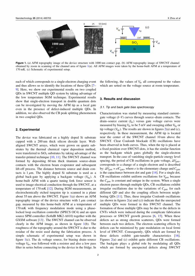
The device was fabricated on a highly doped Si substratecapped with a 200 nm thick silicon dioxide layer. Well-aligned SWCNT arrays, which were grown on quartz sub-strates by the thermal chemical vapor deposition method,were transferred to SiO2 substrates by taking advantage of thetransfer-printed technique [10, 11]. The SWCNT channel wasformed by depositing 60 nm thick titanium source–draincontacts with the electron beam evaporator and subsequentlift-off process. The distance between source and drain con-tacts is μ1 m. The highly doped Si substrate is used as aglobal back-gate by applying a backgate voltage V( )bg . Ahome-built AFM with a quartz tuning fork force sensor isused to image electrical conduction through the SWCNT, at atemperature of 170 mK [12]. During SGM measurements, anelectrochemically etched tungsten tip is scanned in a planeabout 55 nm above the SWCNT. Figure 1(a) shows an AFMtopography image of the device structure with μ1 m contactgap, measured by this home-built AFM at a temperature of170 mK with frequency modulation mode using a phase-locked loop oscillation controller (SPECS OC4) and an opensource SPM controller (SoftdB MK2-A810) together with theGXSM software [13] . The SWCNT channel can be observedclearly in the AFM image, as shown in figure 1(b). Theroughness of the topography around the SWCNT is due to theresidue of the resist used during the fabrication process. Asimple schematic of experimental setup was shown infigure 1(c). The dc voltage source, for biasing drain–sourcevoltage Vds, was followed with a resistor and also a low passfilter in series before connecting to the device in the fridge. In
the following, the values of Vds all correspond to the valueswhich are setted on the voltage source at room temperature.
3. Results and discussion
3.1. Tip and back gate bias spectroscopy
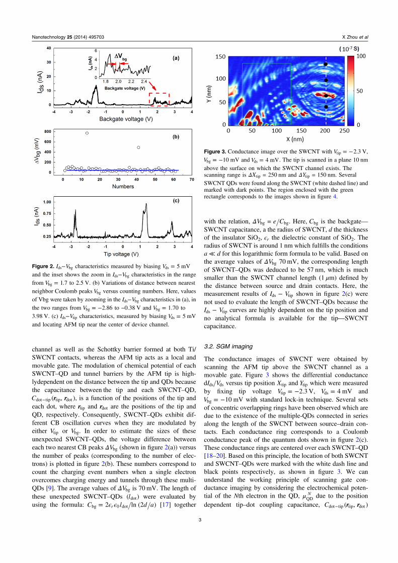
Characterization was started by measuring standard current–gate voltage (I–V) curves through source–drain contacts. Thedrain–source current I( )ds versus gate voltage curves weremeasured by biasingVds to be 5 mV and sweeping eitherVbg ortip voltage V( )tip . The results are shown in figures 2(a) and (c),respectively. In these measurement, the AFM tip is locatednear the center of the SWCNT channel 10 nm above theSWCNT. Clear Coulomb blockade (CB) oscillations havebeen observed in both curves. Thus, when the tip is placed ata fixed position over SWCNT-dots, it has the similar functionas the backgate which gates globally the single-electrontransport. In the case of vanishing single-particle energy levelspacing, the period of CB oscillations in gate voltage, ΔVgate,corresponds to a change of a single electron and is describedby: ΔVgate = e/Cgate, where e is the elementary charge andCgate
is the capacitance between dot and gate [14]. For a single dot,CB oscillations exhibit uniform oscillations for Vgate becausethe Cgate is constant and unique in the system. When a singleelectron passes through multiple QDs, CB oscillations exhibitirregular oscillations due to the variations of Cgate for eachdifferent QD and also the coupling effects between neigh-boring QDs [11]. Thus, these irregular Coulomb oscillations(as shown in figures 2(a) and (c)) indicate that the unexpectedmultiple QDs were formed in this SWCNT channel. Theformation of those multiple QDs may be due to the defects inCNTs which were induced during the complicate fabricationprocesses or SWCNT growth process [6, 15]. When thesedefects act as strong electron scatterers, QDs were formedbetween each two defects. The electron scattering effects bydefects can be minimized by gate modulation on local fermilevel of SWCNT. Consequently, QDs which are formed bythese defects exhibit gate-tunable characteristics [16].Figures 2(a) and (c) exhibit quite different CB oscillations.The backgate plays a global role by modulating all QDswhich are formed by unexpected defects along SWCNT
Figure 1. (a) AFM topography image of the device structure with 1000 nm contact gap. (b) AFM topography image of SWCNT channelobtained by zoom in scanning of the channel area of figure 1(a). All AFM images were taken by the home-built AFM at a temperature of170 mK. (c) Schematic of experimental setup.
2
Nanotechnology 25 (2014) 495703 X Zhou et al
channel as well as the Schottky barrier formed at both Ti/SWCNT contacts, whereas the AFM tip acts as a local andmovable gate. The modulation of chemical potential of eachSWCNT–QD and tunnel barriers by the AFM tip is high-lydependent on the distance between the tip and QDs becausethe capacitance between the tip and each SWCNT–QD,
− r rC ( , )dot tip tip dot , is a function of the positions of the tip andeach dot, where rtip and rdot are the positions of the tip andQD, respectively. Consequently, SWCNT–QDs exhibit dif-ferent CB oscillation curves when they are modulated byeither Vtip or Vbg. In order to estimate the sizes of theseunexpected SWCNT–QDs, the voltage difference betweeneach two nearest CB peaks ΔVbg (shown in figure 2(a)) versusthe number of peaks (corresponding to the number of elec-trons) is plotted in figure 2(b). These numbers correspond tocount the charging event numbers when a single electronovercomes charging energy and tunnels through these multi-QDs [9]. The average values of ΔVbg is 70 mV. The length ofthese unexpected SWCNT–QDs (ldot) were evaluated byusing the formula: ϵ ϵ=C l d a2 ln (2 )rbg 0 dot [17] together
with the relation, ΔVbg = e Cbg. Here, Cbg is the backgate—SWCNT capacitance, a the radius of SWCNT, d the thicknessof the insulator SiO2, ϵr the dielectric constant of SiO2. Theradius of SWCNT is around 1 nm which fulfills the conditionsa ≪ d for this logarithmic form formula to be valid. Based onthe average values of ΔVbg 70 mV, the corresponding lengthof SWCNT–QDs was deduced to be 57 nm, which is muchsmaller than the SWCNT channel length (1 μm) defined bythe distance between source and drain contacts. Here, themeasurement results of −I Vds tip shown in figure 2(c) werenot used to evaluate the length of SWCNT–QDs because the
−I Vds tip curves are highly dependent on the tip position andno analytical formula is available for the tip—SWCNTcapacitance.
3.2. SGM imaging
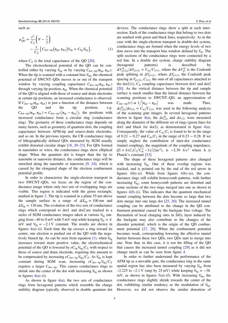
The conductance images of SWCNT were obtained byscanning the AFM tip above the SWCNT channel as amovable gate. Figure 3 shows the differential conductanceI Vd ds ds versus tip position Xtip and Ytip which were measuredby fixing tip voltage = −V 2.3tip V, =V 4ds mV and
= −V 10bg mV with standard lock-in technique. Several setsof concentric overlapping rings have been observed which aredue to the existence of the multiple-QDs connected in seriesalong the length of the SWCNT between source–drain con-tacts. Each conductance ring corresponds to a Coulombconductance peak of the quantum dots shown in figure 2(c).These conductance rings are centered over each SWCNT–QD[18–20]. Based on this principle, the location of both SWCNTand SWCNT–QDs were marked with the white dash line andblack points respectively, as shown in figure 3. We canunderstand the working principle of scanning gate con-ductance imaging by considering the electrochemical poten-tial of the Nth electron in the QD, μ N
QD due to the positiondependent tip–dot coupling capacitance, − r rC ( , )dot tip tip dot
and the inset shows the zoom in −I Vds bg characteristics in the range
from =V 1bg .7 to 2.5 V. (b) Variations of distance between nearest
neighbor Coulomb peaks Vbg versus counting numbers. Here, values
of Vbg were taken by zooming in the −I Vds bg characteristics in (a), in
the two ranges from = −V 2.86bg to −0.38 V and =V 1.70bg to
3.98 V. (c) −I Vds tip characteristics, measured by biasing =V 5ds mV
and locating AFM tip near the center of device channel.
Figure 3. Conductance image over the SWCNT with = −V 2.3tip V,
= −V 10 mVbg and =V 4 mVds . The tip is scanned in a plane 10 nm
above the surface on which the SWCNT channel exists. Thescanning range is ΔXtip = 250 nm and ΔYtip = 150 nm. Several
SWCNT QDs were found along the SWCNT (white dashed line) andmarked with dark points. The region enclosed with the greenrectangle corresponds to the images shown in figure 4.
3
Nanotechnology 25 (2014) 495703 X Zhou et al
such as
μ = −
− +Σ
Σ−
⎜ ⎟⎛⎝
⎞⎠
( ){ }r r
e
CN
e
CC V C V
1
2
, , (1)
NQD
2
dot tip tip dot tip bg bg
where ΣC is the total capacitance of the QD [20].The electrochemical potential of the QD can be con-
trolled either by varying Vtip or by varying − r rC ( , )dot tip tip dot .When the tip is scanned with a constant biasVtip, the chemicalpotential of SWCNT–QDs moves in or out of the transportwindow by varying coupling capacitance − r rC ( , )dot tip tip dot
through varying tip position, rtip. When the chemical potentialof the QD is aligned with those of source and drain electrodesat certain tip positions, an increased conductance is observed.If − r rC ( , )dot tip tip dot is just a function of the distance betweenthe QD and the tip position, e.g.
= −− −r r r rC C( , ) ( )dot tip tip dot dot tip tip dot , the positions withincreased conductance form a circular ring (conductancering). The geometry of these conductance rings depends onmany factors, such as geometry of quantum dots, the couplingcapacitance between AFM-tip and source-drain electrodes,and so on. In the previous reports, the CB conductance ringsof lithographically defined QDs measured by SGM usuallyexhibit distorted circular shape [18, 20–23]. For QDs formedin nanotubes or wires, the conductance rings show ellipticalshape. When the quantum dot is longer than the tip tonanotube or nanowire distance, the conductance rings will bestretched along the nanotube or nanowire [9, 24], which iscaused by the elongated shape of the electron confinementpotential profile.
In order to characterize the single-electron transport intwo SWCNT–QDs, we focus on the region of the con-ductance image where only two sets of overlapping rings arevisible. This region is indicated with the green rectangle,marked in figure 3. The tip is scanned in a plane 55 nm abovethe sample surface in a range of Δ =X 100tip nm andΔ =Y 130tip nm. The evolution of the two sets of conductancerings which correspond to dot1 and dot2 are tracked in aseries of SGM conductance images taken at various Vbg ran-ging from −40 to 0 mV with 5 mV step while keeping =V 4ds
mV and = −V 2.1tip V constant. The results are shown infigures 4(a)–(i). Each time the tip crosses a ring toward itscenter, one electron is pushed out of the QD with the nega-tively biased tip. As can be seen from equation (1), when Vbg
increases toward more positive value, the electrochemicalpotential of the QD is lowered by ΣeC V Cbg bg with respect tothose of source and drain electrode, requiring this amount tobe compensated by increasing Σ−eC V Cdot tip tip . As Vtip is keptconstant during SGM scan, increasing Σ−eC V Cdot tip tip
requires a larger −Cdot tip. This causes conductance rings toshrink into the center of the dot with increasing Vbg as shownin figures 4(a)–(i).
As shown in figure 4(a), the two sets of conductancerings form hexagonal patterns which resemble the chargestability diagram typically observed in double quantum dot
devices. The conductance rings show a split at each inter-section. Each of the conductance rings that belong to two dotsare marked with green and black lines, respectively. As in thecase with the single-electron transport in double-dot system,conductance rings are formed when the energy levels of twodots move into the transport bias window defined by Vds. Thesplit sections of the conductance rings were connected by ared line. In a double dot system, charge stability diagram(hexagonal patterns) is described byΔ Δ =V V C Cg g1(2)
m1(2) m 2(1) , where the ΔVg1
m is the Coulombpeak splitting in ΔVg1(2) , where ΔVg1(2) the Coulomb peakspacing in Vg1(2) , C2(1) the sum of all capacitances attached tothe dot2(1), Cm coupling capacitance between dot1 and dot2[20]. As the vertical distance between the tip and samplesurface is much smaller than the lateral distance between thescanning positions to SWCNT–QD, an approximation of
∝ −− r rC r( ) 1dot tip tip dot was made. Thus,
Δ Δ =r r C C1(2)m
1(2) m 2(1) was used in the following analysisof the scanning gate images. In several hexagonal patternsshown in figure 4(a), the Δr1(2)
m and Δr1(2) were measuredalong the diameter of the different set of rings (green lines fordot1 and black for dot2), as demonstrated in figure 4(a).Consequently, the value of C Cm 1 is found to be in the rangeof 0.21 ∼ 0.27 and C Cm 2 in the range of 0.23 ∼ 0.28. If wesimply neglect the contribution of inter-dot conductance(tunnel coupling), the magnitude of the coupling impedance,
π= −Z h C C C e( 1) (2 )1 2 m2 2 , is ∼2.39 h e2 where h is
Planckʼs constant [23].The shape of these hexagonal patterns also changed
with increasing Vbg. One of these overlap regions wastracked, and is pointed out by the end of the red arrow infigures 4(b)–(i). While from figures 4(b)–(e), the con-ductance rings still exhibit honeycomb patterns, with furtherincreasing Vbg, some honeycomb patterns are distorted andsome sections of the two rings merged into one as shown infigures 4(f)–(i). This indicates that the quantum mechanicaltunnel coupling between the dots become so large that twodots merge into one large dot [25, 26]. The increased tunnelcoupling can be attributed to the change in the QD con-finement potential caused by the backgate bias voltage. Thefluctuation of local charging sites in SiO2 layer induced bythe backgate may also contribute to the changes of thedisorder potential, which is the origin of the QD confine-ment potential [27, 28]. When the confinement potentialbecomes weak, corresponding lowering the effective tunnelbarrier between these two QDs, two QDs start to merge intoone. Note that, in this case, it is not the filling of the QDthat causes the increased tunnel coupling [29] as it did notchange much as can be seen from figure 4.
In order to further understand the performance of theAFM tip as a movable gate, the conductance ring in the samespatial region has also been measured by varying Vtip from−2.225 to −2.1 V (step by 25 mV) while keeping = −V 38bg
mV, as shown in figures 5(a)–(f). With increasing Vtip, theconductance rings slightly shrink towards the center of thedot, exhibiting similar tendency as the modulation of Vbg.However, we did not observe the similar distortion of
4
Nanotechnology 25 (2014) 495703 X Zhou et al
conductance rings which have been observed by modulationof Vbg. In order to make comparison between Cbg and −Cdot tip,the motion of one conductance ring was tracked by changingVbg or Vtip. As shown in figures 4(a)–(d), values of Vbg arevaried from −40 to −25 mV while keeping = −V 2.1tip V
constant, which cause Nth conductance ring to move towardsthe center by one ring spacing. As shown in figure 4(d), theNth conductance ring almost reaches the position of N-1thconductance ring in figure 4(a) at = −V 25bg mV. Thus, wecan conclude that 15 mV is needed to remove one electron
Figure 4. (a)–(i) Conductance images of the SWCNT taken at different backgate bias voltages, Vbg. The Vbg was varied from −40 to 0 mV
with a step of 5 mV. =V 4ds mV and = −V 2.1tip V were kept constant during the measurement. The tip scanning range was within green
rectangle, marked in figure 3. The overlapping two sets of rings form hexagon patterns. The conductance rings of dot1 and dot2 are marked ingreen and black lines, respectively. Two of these conductance rings of dot1 are marked Nth and N-1th. In order to make a position reference,the position of the initial Nth conductance ring at = −V 40bg mV was marked with white dash line from (a) to (i). With increasingVbg, the Nth
conductance ring moves towards the N-1th ring. When = −V 25bg mV, the Nth conductance ring moves from the white dashed line to the
solid white line marked as N which was the previous position of the N-1th ring in figure 4(a), as shown in figure 4(d). (a) Shows how thevalues of Δr1
m and Δr1 were obtained from the conductance image in (a).
5
Nanotechnology 25 (2014) 495703 X Zhou et al
from dot. However, when Vtip is varied from −2.225 to−2.1 V, no conductance ring moves over one ring spacing asshown in figures 5(a)–(f). In other words, it means the −Cdot tip
is much smaller than Cbg, because e = Δ−C Vdot tip tip = ΔC Vbg bg
[9]. Based on above measurement, the upper bound of theratio −C Cdot tip bg is estimated to be 0.12. This is because theAFM tip is far from the SWCNT-dots which makes the
−Cdot tip relatively small.
3.3. Observation of peak splitting
For coupled double dots, the split of CB conductance peakscan be caused by capacitive coupling and tunnel coupling[30]. Classical interdot capacitive coupling which reduces theenergy of polarized charge configuration leads to conductancepeak splitting. However, it requires that the interdot couplingcapacitance increase strongly while the interdot tunnel con-ductance remains negligible [31–33]. When interdot tunnelconductance is no longer negligible, quantum fluctuationsbetween dots also cause peak splitting [31, 34]. In both cases,the separation of the peak splitting indicates the couplingstrength between these two dots because the separation ofpeak splitting is proportional to the coupling strengthregardless of coupling mechanism.
In the SGM measurement, the inter-dot coupling phe-nomenon can be observed by varying Vtip or tip position.
Here, we still focus on the double dot system where thereare only two sets of overlapping rings. One of the typicalconductance image was taken by biasing = −V 2tip V,
= −V 72bg mV and scanning tip in a range of Δ =X 150tip
nm and Δ =Y 150tip nm, as shown in figure 6. Here, thescanned region is different from the region shown infigure 4 and figure 5. Four different scanned regions havebeen marked (A)–(D) in figure 6. In the region (A), twoconductance rings which belong to two different SWCNT-dots starts to bend and split. In contrast to the region (A), inthe region (B)–(D), two conductance rings just overlap anddo not clearly split in the overlap region. Figure 7 shows the
−I Vds tip curves measured at the positions marked as theblack point in each region (A)–(D) in figure 6 by biasing
=V 5ds mV, = −V 75bg mV and sweeping Vtip from −2.2 to−1.8 V. We focus on these Coulomb peaks around = −V 2tip
V, as the conductance image in the figure 6 was measuredby biasing = −V 2tip V. At position (A), at around = −V 2tip
V, single-electron transport is Coulomb blockaded as thereis no Coulomb peak at this voltage. It is consistent that thereis no conductance at the black point position in the con-ductance image, which indicates the energy levels of thedouble-dots do not align in the transport window. However,in the position (B)–(C), the Coulomb peaks at around
= −V 2tip V exhibit the weakly split peaks which indicate theweaker inter-dot coupling, as shown in figure 7(B)–(C). In
Figure 5. (a)–(f) Conductance images taken at different tip bias voltages, Vtip. The Vtip was varied from −2.225 to −2.100 V with a step of
25 mV with keeping = −V 38bg mV constant. We still keep on tracking the same Nth and N-1th conductance rings which are marked on
figure 4(a). With increasing Vtip, the Nth conductance rings moves slightly towards to the N-1th conductance rings. However, when
= −V 2.1tip V, the Nth conductance rings, which are marked in a solid white line as N , are still far from the position of N-1th conductance
rings in figure 5(a), as shown in figure 5(f).
6
Nanotechnology 25 (2014) 495703 X Zhou et al
position (D), the peak clearly splits into two peaks. The splitpeak separation is 28 mV around = −V 2tip V and 33 mVaround = −V 1.9tip V, which is due to the increases of theinter-dot coupling effects [34]. However, from SGM images,it is difficult to determine the mechanism of inter-dotinteractions by directly measuring the inter-dot conductance
as previous reports [25, 35] because the stability diagram(SGM images) obtained with SGM technique is morecomplex than typical stability diagram obtained by sweepinggate bias voltages. In order to verify the inter-dot couplingmechanism for defect-induced tunnel barriers in SWCNT–QDs, further investigation is still required.
Figure 6. (Left) Conductance image taken at = −V 2tip V, = −V 72bg mV. (Right) (A)–(D) zoomed in images of the positions A–B indicated
in the left image, respectively.
Figure 7. −V Itip ds characteristics measured by locating tip at position (A)–(D) marked as red points in figure 6. Here, −V Itip ds characteristics
were obtained by biasing =V 5ds mV, = −V 75bg mV and sweeping Vtip from −2.2 to −1.8 V.
7
Nanotechnology 25 (2014) 495703 X Zhou et al
4. Conclusion
Two coupled SWCNT QDs in multiple-QD systems havebeen characterized by taking advantage of low temperatureSGM measurement technique. The conductance images of theSWCNT channel exhibit several sets of conductance rings,which indicate the locations of these multiple-QDs along theSWCNT. The modulation of single-electron transport inSWCNT double QDs can be achieved by changing tip posi-tion and Vtip. The typical hexagonal patterns of coupleddouble dots have been clearly observed in conductance ima-ges. The capacitance between AFM-tip and SWCNT-dotswas less than 12% of the backgate capacitance. Based onconductance image of coupled two dots, the values of cou-pling capacitance between two SWCNT-dots over totalcapacitance of each dot were also evaluated to be
= ∼C C 0.21 0.27m 1 and = ∼C C 0.23 0.28m 2 , respec-tively. In addition, the typical inter-dot coupling phenom-enon, Coulomb peak splitting, also has been observed byvarying the AFM tip position. The measurement resultsdemonstrate the advantages of low temperature of SGMmeasurement technique.
Acknowledgments
Xin ZHOU was supported by the Special PostdoctoralResearch Program of RIKEN and this research was alsosupported by NanoQuebec.
References
[1] Kuemmeth F, Churchill H O, Herring P K and Marcus C M2002 Mater. Today 13 18
[2] Katsnelson M I and Geim A K 2008 Phil. Trans. R. Soc. A 366[3] Cobden D H, Bockrath M, McEuen P L, Rinzler A G and
Smalley R E 1998 Phys. Rev. Lett. 81 681[4] Nygard J, Cobden D H and Lindelof P E 2000 Nature 408 342[5] Jarillo-Herrero P, Sapmaz S, Dekker C, Kouwenhoven L P and
van der Zant H S J 2004 Nature 429 389[6] Biercuk M J, Ilani S, Marcus C M and McEuen P L 2008
Carbon Nanotubes (Topics in Applied Physics vol 111)(Berlin: Springer) p 455
[7] Bleszynski-Jayich A C, Froberg L E, Bjork M T, Trodahl H J,Samuelson L and Westervelt R M 2008 Phys. Rev. B 77245324
[8] Woodside M T and McEuen P L 2002 Science 296 1098[9] Boyd E E, Storm K, Storm L, Samuelson L and
Westervelt R M 2011 Nanotechnology 22 185201[10] Tabata H, Shimizu M and Ishibashi K 2009 Appl. Phys. Lett.
95 113107[11] Zhou X and Ishibashi K 2012 Appl. Phys. Lett. 101 123506
[12] Hedberg J A, Lal A, Miyahara Y, Grutter P, Gervais G,Hilke M, Pfeiffer L and West K W 2010 Appl. Phys. Lett. 97143107
Hedberg J A 2011 PhD Thesis McGill University[13] Zahl P, Bierkandt M, Shrder S and Klust A 2003 Rev. Sci.
Instrum. 74 1222[14] Kouwenhoven L P, van der Vaart N C, Johnson A T, Kool W,
Harmans C J P M, Williamson J G, Staring A A M andFoxon C T 1991 Z. Phys. B 85 367
[15] Ishibashi K, Moriyama S, Tsuya D, Fuse T and Suzuki M 2006J. Vac. Sci. Technol. A 24 1349
[16] Bockrath M, Liang W, Bozovic D, Hafner J H, Lieber C M,Tinkham M and Park H 2001 Science 291 283
[17] Yao Z, Dekker C and Avouris P 2001 ed M S Dresselhaus,G Dresselhaus and Ph Avouris Electrical transport throughsingle-wall carbon nanotubes Topics in Applied Physics vol80 (Berlin: Springer) p 147
[18] Fallahi P, Bleszynski A C, Westervelt R M, Huang J,Walls J D, Heller E J, Hanson M and Gossard A C 2005Nano Lett. 5 223
[19] Bleszynski A C, Zwanenburg F A, 1Westervelt R M,Roest A L, Bakkers E P A M and Kouwenhoven L P 2007Nano Lett. 7 2559
[20] Bleszynski-Jayich A C, Fröberg L E, Björk M T, Trodahl H J,Samuelson L and Westervelt R M 2008 Phys. Rev. B 77245327
[21] van der Wiel W G, Franceschi S D, Elzerman J M, Fujisawa T,Tarucha S and Kouwenhoven L P 2003 Rev. Mod. Phys.75 1
[22] Schnez S, Guttinger J, Stampfer C, Ensslin K and Ihn T 2011New J. Phys. 13 053013
[23] Huefner M, Kueng B, Schnez S, Ensslin K and Ihn T 2011Phys. Rev. B 83 235326
[24] Brink M 2007 Imaging single-electron charging innanostructures by low-temperature scanning forcemicroscopy PhD Thesis Cornell University
[25] Livermore C, Crouch C H, Westervelt R M, Campman K L andGossard A C 1996 Science 274 1332
[26] Mason N, Biercuk M J and Marcus C M 2004 Science303 655
[27] Waugh F R, Berry M J, Crouch C H, Livermore C, Mar D J,Westervelt R M, Campman K L and Gossard A C 1996Phys. Rev. B 53 1413
[28] Staring A A M, van Houten H, Beenakker C W J andFoxon C T 1992 Phys. Rev. B 45 9222
[29] Brodsky M, Zhitenev N B, Ashoori R C, Pfeiffer L N andWest K W 2000 Phys. Rev. Lett. 85 2356
[30] Ruzin I M, Chandrasekhar V, Levin E I and Glazman L I 1992Phys. Rev. B 45 13469
[31] Waugh F R, Berry M J, Crouch C H, Livermore C,Mar D J and Westervelt R M 1996 Phys. Rev. B 53 1413
[32] Glazman L I and Chandrasekhar V 1992 Europhys. Lett.19 623
[33] Ruzin I M, Chandrasekhar V, Levin E I and Glazman L I 1992Phys. Rev. B 45 469
[34] Waugh F R, Berry M J, Mar D J and Westervelt R M 1995Phys. Rev. Lett. 75 705
[35] DiCarlo L, Lynch H J, Johnson A C, Childress L I, Crockett K,Marcus C M, Hanson M P and Gossard A C 2004 Phys. Rev.Lett. 92 226801