1 Department of Materials Science and Engineering, Northwestern University Scanning Probe Microscopy C. Julian Chen, Introduction to Scanning Tunneling Microscopy Department of Materials Science and Engineering, Northwestern University An Ideal Experiment for Probing Molecular Conduction M. C. Hersam, et al., MRS Bulletin, 29, 385 (2004).
Transcript
1
Department of Materials Science and Engineering, Northwestern University
Scanning Probe Microscopy
C. Julian Chen, Introduction to Scanning Tunneling Microscopy
Department of Materials Science and Engineering, Northwestern University
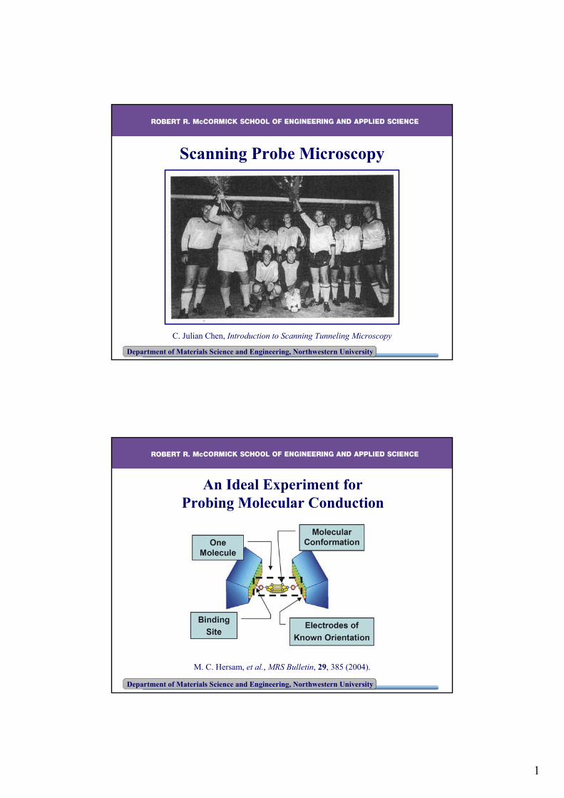
An Ideal Experiment forProbing Molecular Conduction
M. C. Hersam, et al., MRS Bulletin, 29, 385 (2004).
2
Department of Materials Science and Engineering, Northwestern University
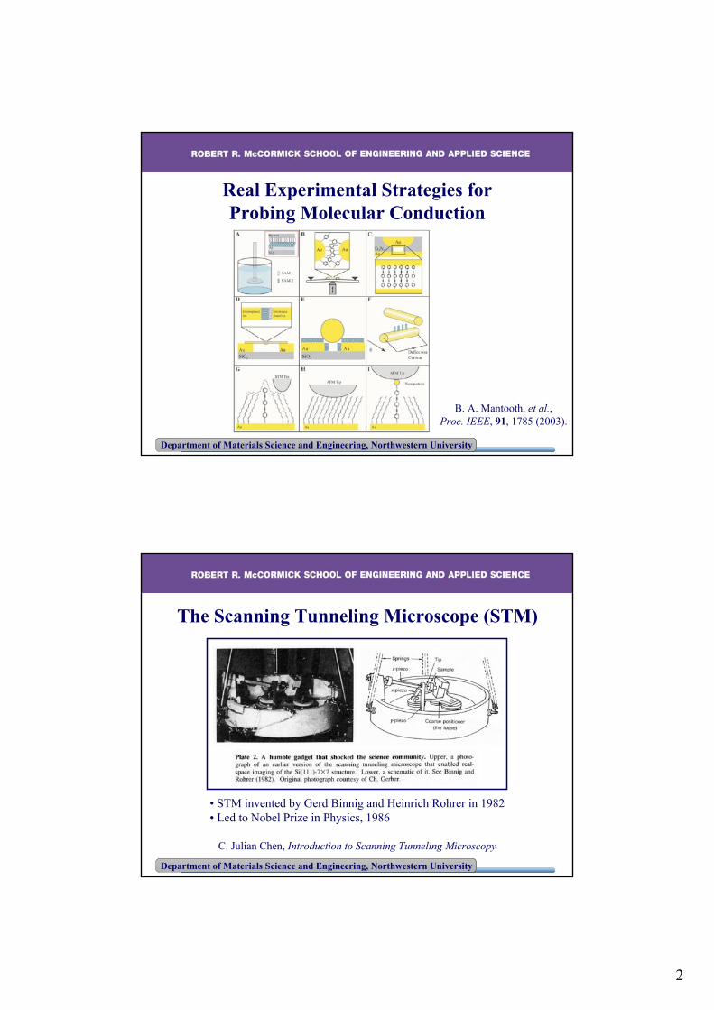
Real Experimental Strategies forProbing Molecular Conduction
B. A. Mantooth, et al.,Proc. IEEE, 91, 1785 (2003).
Department of Materials Science and Engineering, Northwestern University
The Scanning Tunneling Microscope (STM)
• STM invented by Gerd Binnig and Heinrich Rohrer in 1982• Led to Nobel Prize in Physics, 1986
C. Julian Chen, Introduction to Scanning Tunneling Microscopy
3
Department of Materials Science and Engineering, Northwestern University
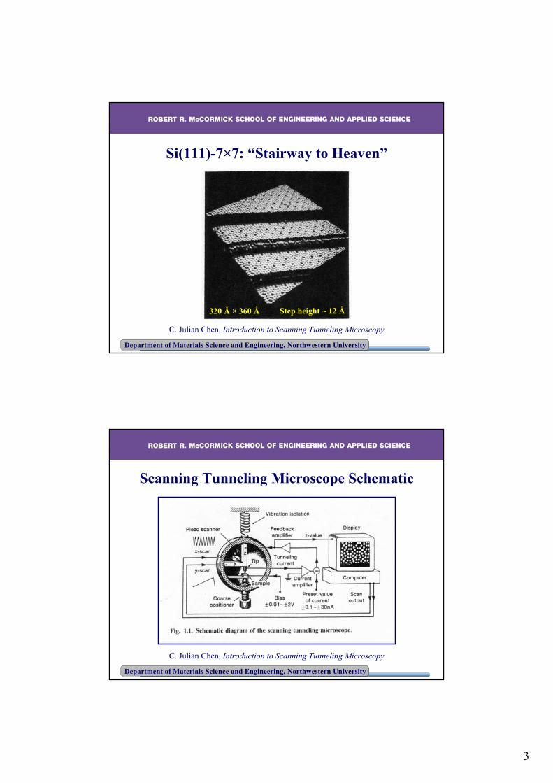
320 Å × 360 Å Step height ~ 12 Å
Si(111)-7×7: “Stairway to Heaven”
C. Julian Chen, Introduction to Scanning Tunneling Microscopy
Department of Materials Science and Engineering, Northwestern University
Scanning Tunneling Microscope Schematic
C. Julian Chen, Introduction to Scanning Tunneling Microscopy
4
Department of Materials Science and Engineering, Northwestern University
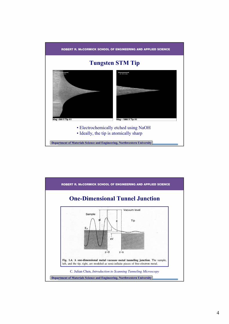
Tungsten STM Tip
• Electrochemically etched using NaOH• Ideally, the tip is atomically sharp
Department of Materials Science and Engineering, Northwestern University
One-Dimensional Tunnel Junction
C. Julian Chen, Introduction to Scanning Tunneling Microscopy
5
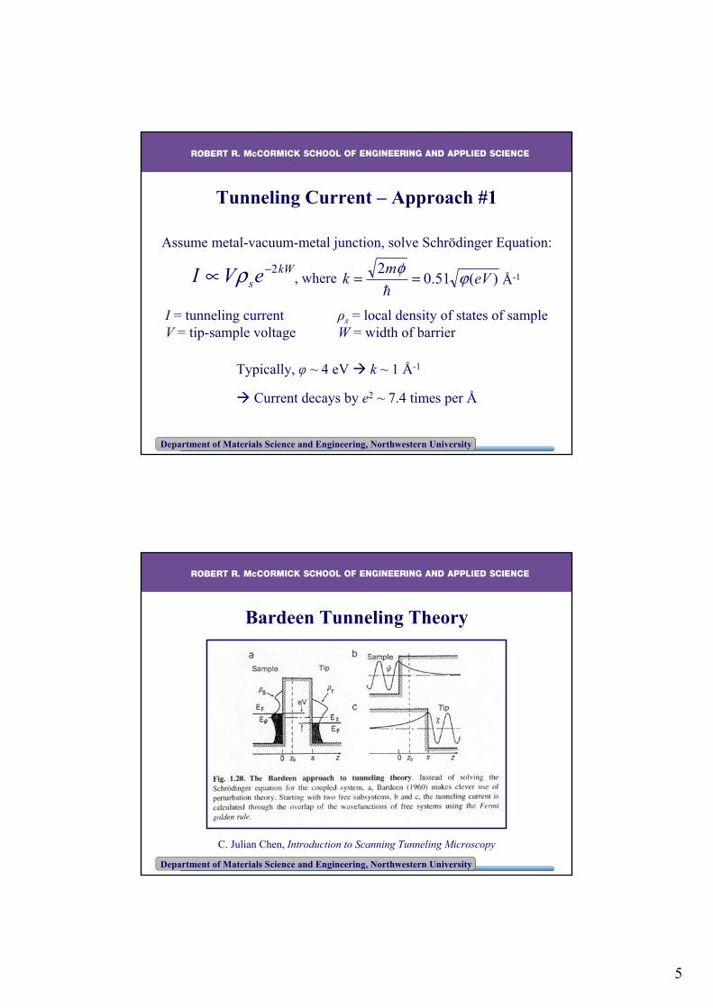
Department of Materials Science and Engineering, Northwestern University
I = tunneling current ρs = local density of states of sampleV = tip-sample voltage W = width of barrier
kWseVI 2−∝ ρ )(51.0
2eV
mk ϕφ
== Å-1, where
Typically, φ ~ 4 eV k ~ 1 Å-1
Current decays by e2 ~ 7.4 times per Å
Department of Materials Science and Engineering, Northwestern University
Bardeen Tunneling Theory
C. Julian Chen, Introduction to Scanning Tunneling Microscopy
6
Department of Materials Science and Engineering, Northwestern University
Tunneling Current – Approach #2
Consider overlap of wavefunctions from either side of barrier:
Using Fermi’s Golden Rule (assuming kT << energy resolutionof the measurement),
For a free electron metal tip, ρt is constant:
)( eVEdVdI
Fs −∝ ρ STM Spectroscopy
∫ ++−∝eV
FtFs dEeVEI0
)()( εερερsample tip
Department of Materials Science and Engineering, Northwestern University
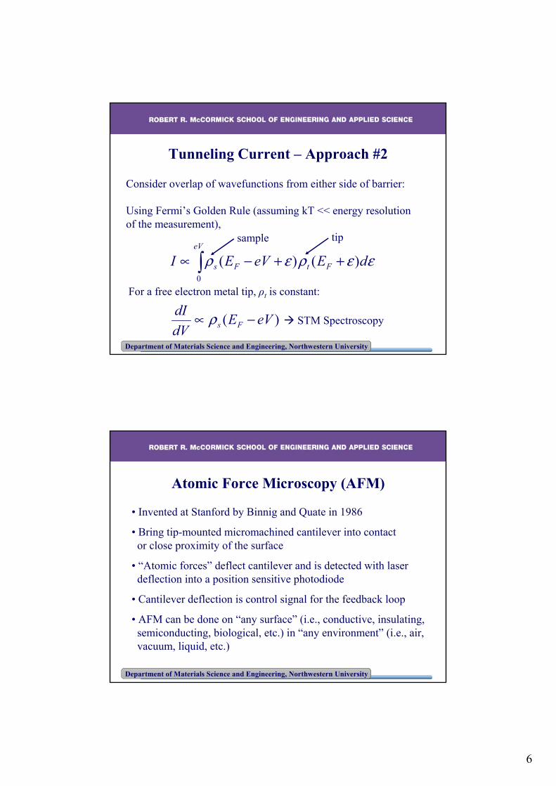
Atomic Force Microscopy (AFM)
• Invented at Stanford by Binnig and Quate in 1986
• Bring tip-mounted micromachined cantilever into contactor close proximity of the surface
• “Atomic forces” deflect cantilever and is detected with laserdeflection into a position sensitive photodiode
• Cantilever deflection is control signal for the feedback loop
• AFM can be done on “any surface” (i.e., conductive, insulating,semiconducting, biological, etc.) in “any environment” (i.e., air,vacuum, liquid, etc.)
7
Department of Materials Science and Engineering, Northwestern University
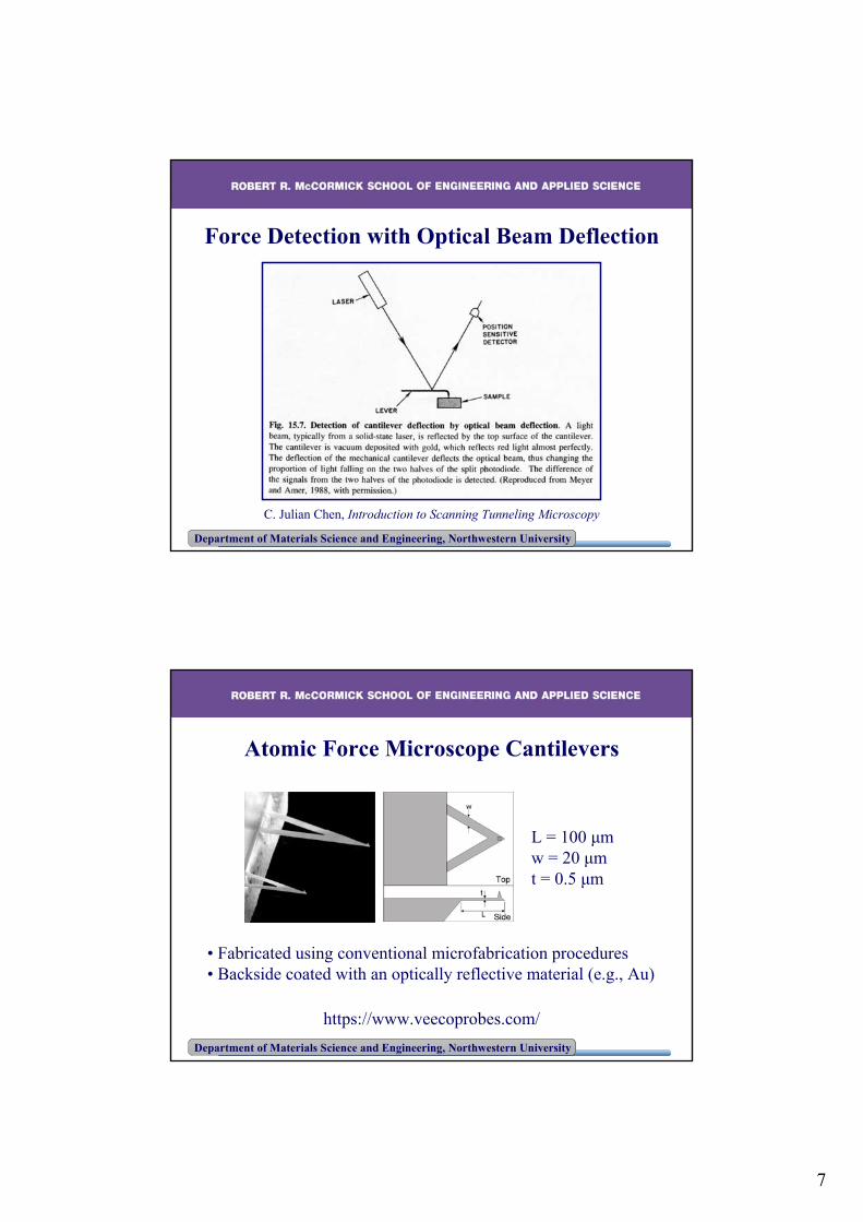
Force Detection with Optical Beam Deflection
C. Julian Chen, Introduction to Scanning Tunneling Microscopy
Department of Materials Science and Engineering, Northwestern University
Atomic Force Microscope Cantilevers
• Fabricated using conventional microfabrication procedures• Backside coated with an optically reflective material (e.g., Au)
https://www.veecoprobes.com/
L = 100 μmw = 20 μmt = 0.5 μm
8
Department of Materials Science and Engineering, Northwestern University
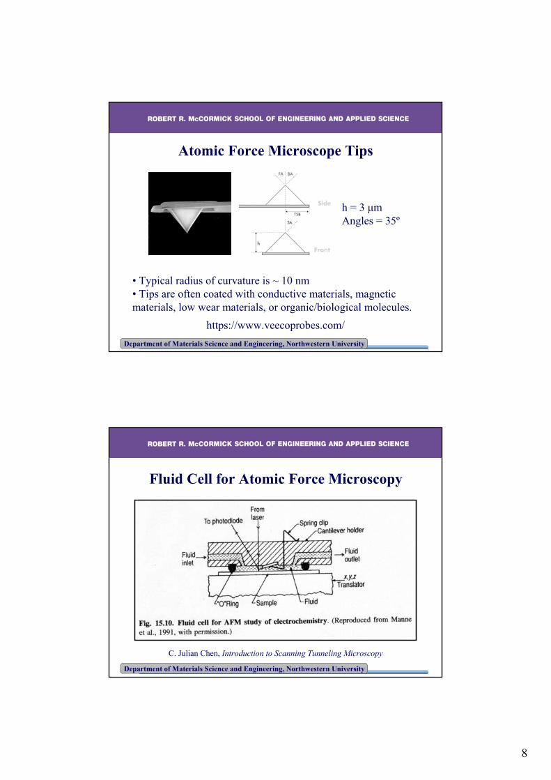
Atomic Force Microscope Tips
• Typical radius of curvature is ~ 10 nm• Tips are often coated with conductive materials, magnetic materials, low wear materials, or organic/biological molecules.
https://www.veecoprobes.com/
h = 3 μmAngles = 35º
Department of Materials Science and Engineering, Northwestern University
Fluid Cell for Atomic Force Microscopy
C. Julian Chen, Introduction to Scanning Tunneling Microscopy
9
Department of Materials Science and Engineering, Northwestern University
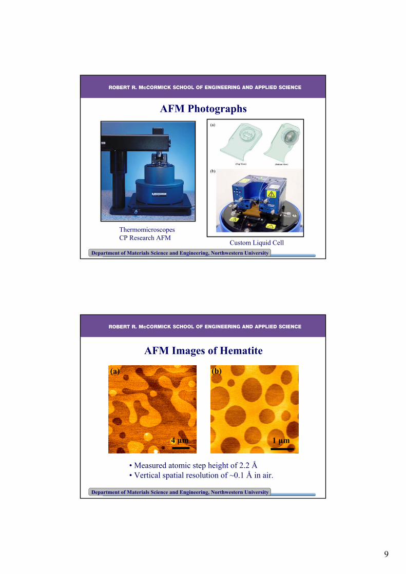
ThermomicroscopesCP Research AFM
Custom Liquid Cell
AFM Photographs
Department of Materials Science and Engineering, Northwestern University
AFM Images of Hematite
(b)
1 μm
(a)
4 μm
• Measured atomic step height of 2.2 Å• Vertical spatial resolution of ~0.1 Å in air.
10
Department of Materials Science and Engineering, Northwestern University
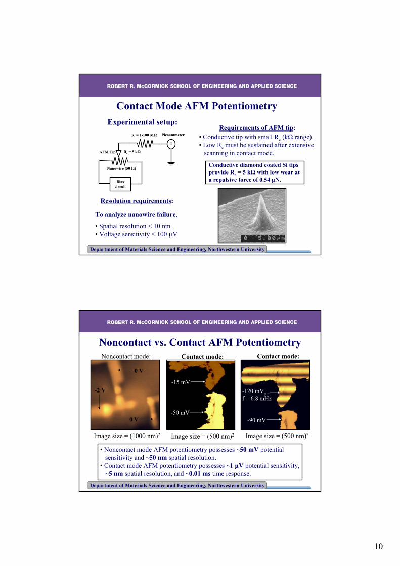
Contact Mode AFM Potentiometry
Biascircuit
Nanowire (50 Ω)
I
AFM Tip
Rl = 1-100 MΩ Picoammeter
Rc = 5 kΩ
Experimental setup:Requirements of AFM tip:
• Conductive tip with small Rc (kΩ range).• Low Rc must be sustained after extensive
M. C. Hersam, et al., Appl. Phys. Lett., 72, 915 (1998).
Department of Materials Science and Engineering, Northwestern University
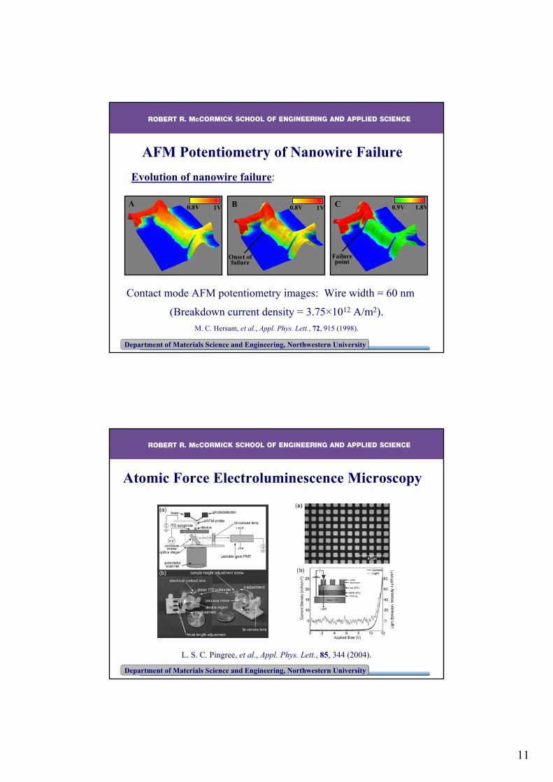
Atomic Force Electroluminescence Microscopy
L. S. C. Pingree, et al., Appl. Phys. Lett., 85, 344 (2004).
12
Department of Materials Science and Engineering, Northwestern University
AFEM on Organic LED Arrays
Current Map Light Emission Map Quantum Efficiency Map
Department of Materials Science and Engineering, Northwestern University
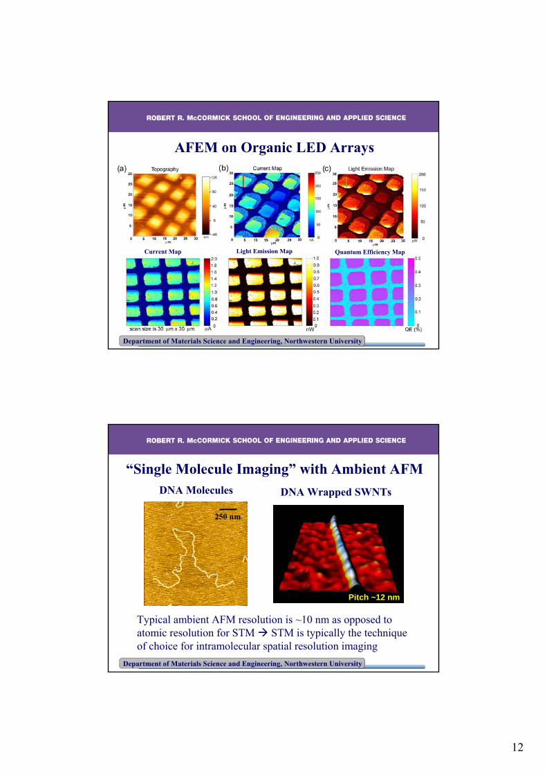
250 nm
DNA Molecules
Pitch ~12 nm
DNA Wrapped SWNTs
“Single Molecule Imaging” with Ambient AFM
Typical ambient AFM resolution is ~10 nm as opposed to atomic resolution for STM STM is typically the technique of choice for intramolecular spatial resolution imaging
13
Department of Materials Science and Engineering, Northwestern University
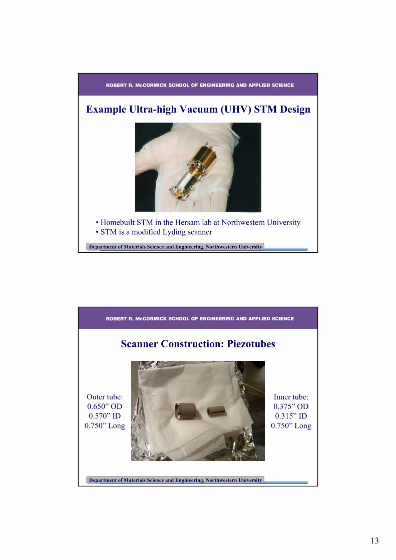
Example Ultra-high Vacuum (UHV) STM Design
• Homebuilt STM in the Hersam lab at Northwestern University• STM is a modified Lyding scanner
Department of Materials Science and Engineering, Northwestern University
Scanner Construction: Piezotubes
Outer tube:0.650” OD0.570” ID
0.750” Long
Inner tube:0.375” OD0.315” ID
0.750” Long
14
Department of Materials Science and Engineering, Northwestern University
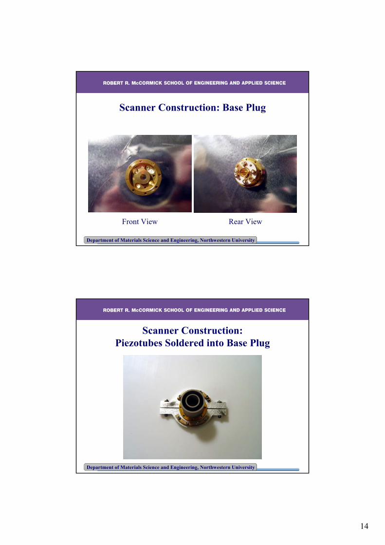
Scanner Construction: Base Plug
Front View Rear View
Department of Materials Science and Engineering, Northwestern University
Scanner Construction:Piezotubes Soldered into Base Plug
15
Department of Materials Science and Engineering, Northwestern University
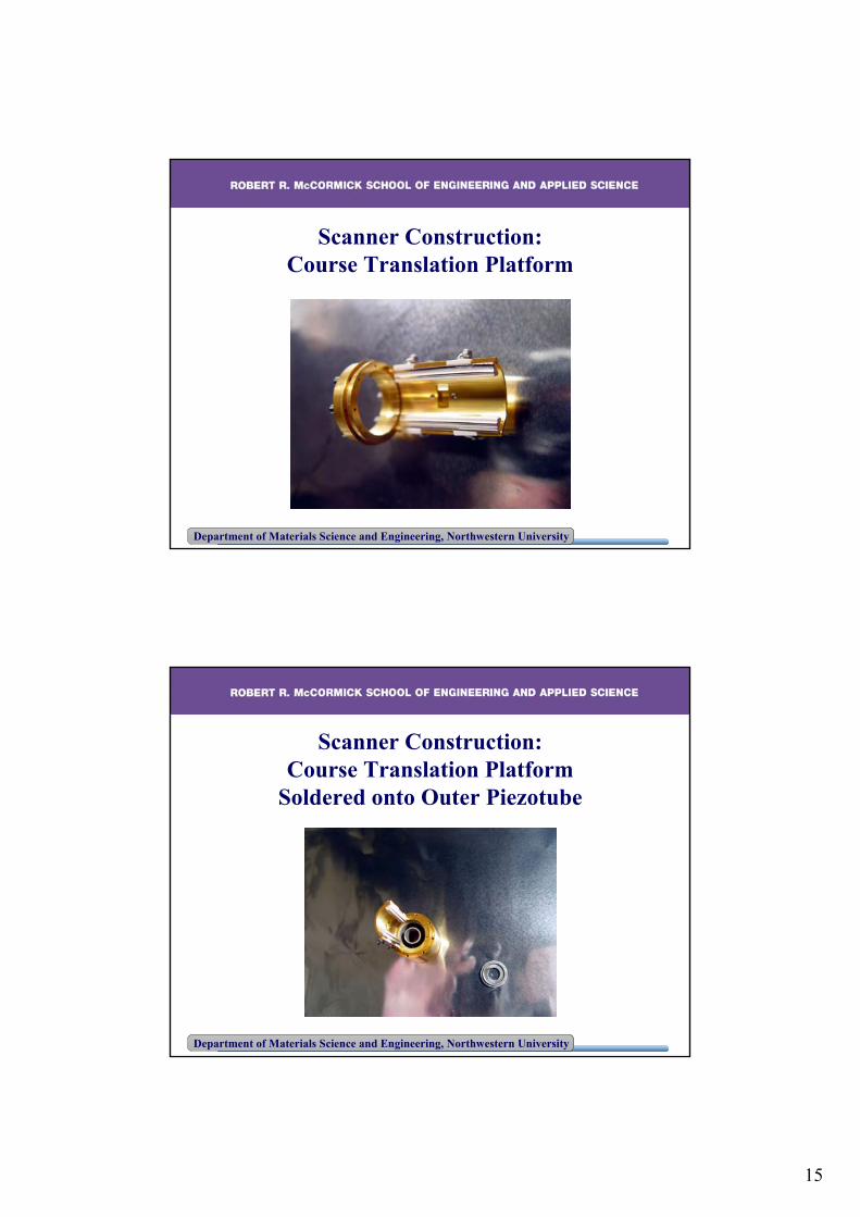
Scanner Construction:Course Translation Platform
Department of Materials Science and Engineering, Northwestern University
Scanner Construction:Course Translation Platform
Soldered onto Outer Piezotube
16
Department of Materials Science and Engineering, Northwestern University
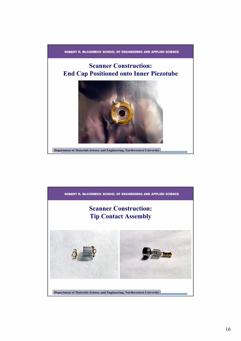
Scanner Construction:End Cap Positioned onto Inner Piezotube
Department of Materials Science and Engineering, Northwestern University
Scanner Construction:Tip Contact Assembly
17
Department of Materials Science and Engineering, Northwestern University
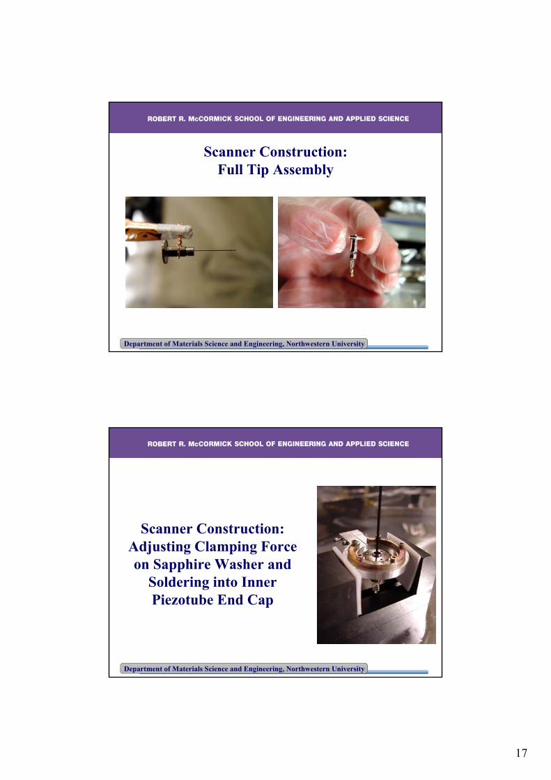
Scanner Construction:Full Tip Assembly
Department of Materials Science and Engineering, Northwestern University
Scanner Construction:Adjusting Clamping Forceon Sapphire Washer and
Soldering into InnerPiezotube End Cap
18
Department of Materials Science and Engineering, Northwestern University
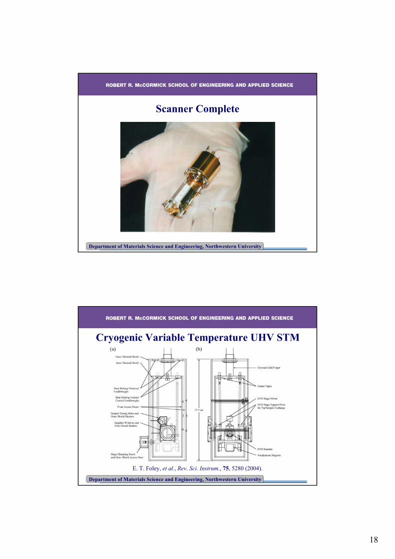
Scanner Complete
Department of Materials Science and Engineering, Northwestern University
Cryogenic Variable Temperature UHV STM
E. T. Foley, et al., Rev. Sci. Instrum., 75, 5280 (2004).
19
Department of Materials Science and Engineering, Northwestern University
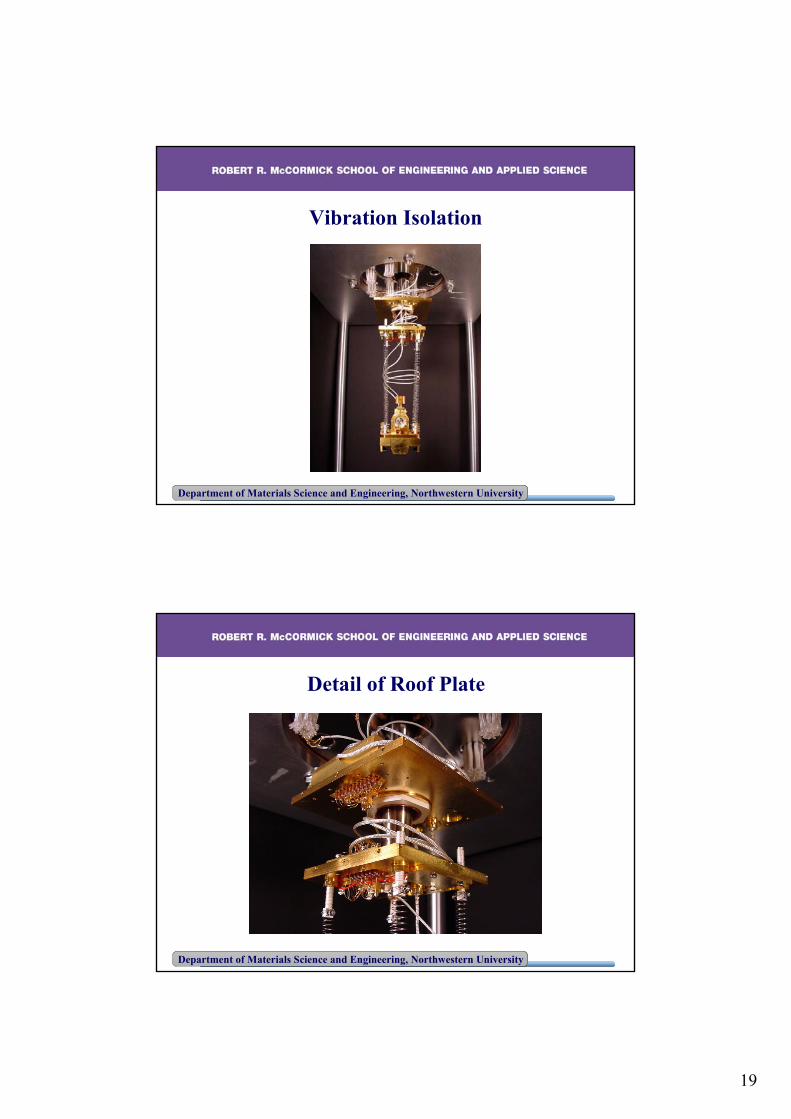
Vibration Isolation
Department of Materials Science and Engineering, Northwestern University
Detail of Roof Plate
20
Department of Materials Science and Engineering, Northwestern University
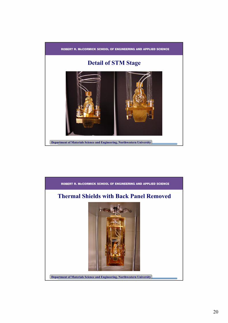
Detail of STM Stage
Department of Materials Science and Engineering, Northwestern University
Thermal Shields with Back Panel Removed
21
Department of Materials Science and Engineering, Northwestern University
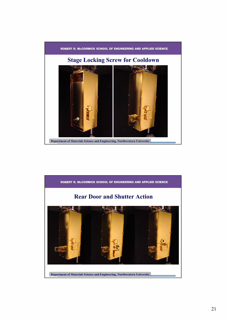
Stage Locking Screw for Cooldown
Department of Materials Science and Engineering, Northwestern University
Rear Door and Shutter Action
22
Department of Materials Science and Engineering, Northwestern University
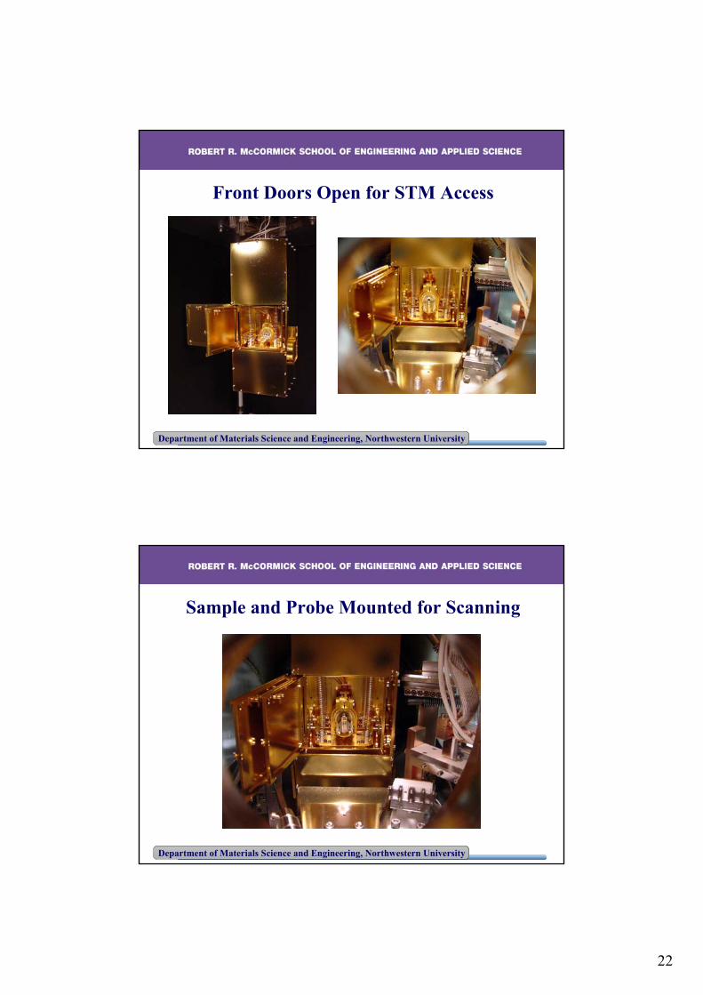
Front Doors Open for STM Access
Department of Materials Science and Engineering, Northwestern University
Sample and Probe Mounted for Scanning
23
Department of Materials Science and Engineering, Northwestern University
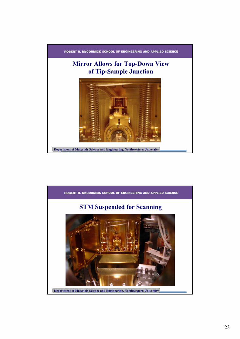
Mirror Allows for Top-Down Viewof Tip-Sample Junction
Department of Materials Science and Engineering, Northwestern University
STM Suspended for Scanning
24
Department of Materials Science and Engineering, Northwestern University
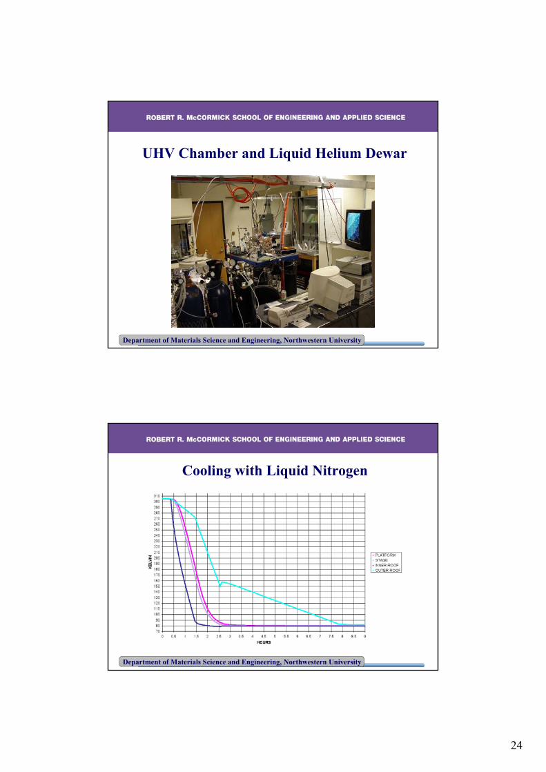
UHV Chamber and Liquid Helium Dewar
Department of Materials Science and Engineering, Northwestern University
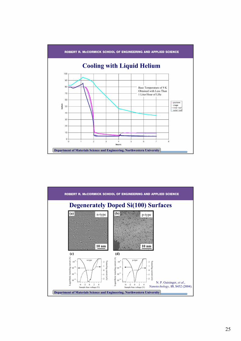
Cooling with Liquid Nitrogen
25
Department of Materials Science and Engineering, Northwestern University
Base Temperature of 9 KObtained with Less Than1 Liter/Hour of LHe
Cooling with Liquid Helium
Department of Materials Science and Engineering, Northwestern University
(c)
10-12
10-11
10-10
10-9
Loga
rithm
ic tu
nnel
ing
curr
ent (
A)
-4 -2 0 2 4Sample bias voltage (V)
-2
-1
0
1
2
Tunneling current (nA)
n-type
(d)
10-12
10-11
10-10
10-9
Loga
rithm
ic tu
nnel
ing
curr
ent (
A)
-4 -2 0 2 4Sample bias voltage (V)
-2
-1
0
1
2
Tunneling current (nA)
p-type
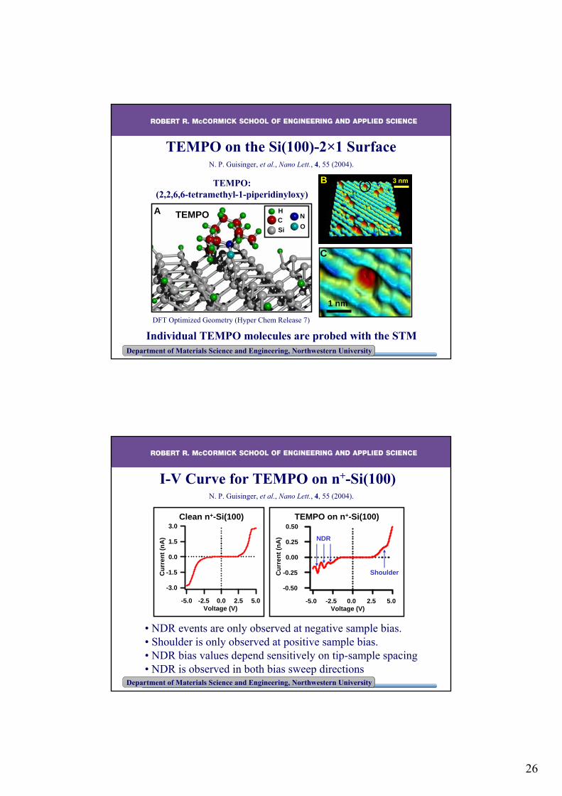
10 nm
(a) n-type
10 nm
(b) p-type
Degenerately Doped Si(100) Surfaces
N. P. Guisinger, et al.,Nanotechology, 15, S452 (2004).
26
Department of Materials Science and Engineering, Northwestern University
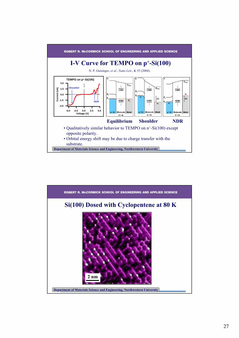
TEMPO on the Si(100)-2×1 Surface
B 3 nm
1 nm
C
A TEMPO NO
HCSi
TEMPO:(2,2,6,6-tetramethyl-1-piperidinyloxy)
DFT Optimized Geometry (Hyper Chem Release 7)
Individual TEMPO molecules are probed with the STM
N. P. Guisinger, et al., Nano Lett., 4, 55 (2004).
Department of Materials Science and Engineering, Northwestern University
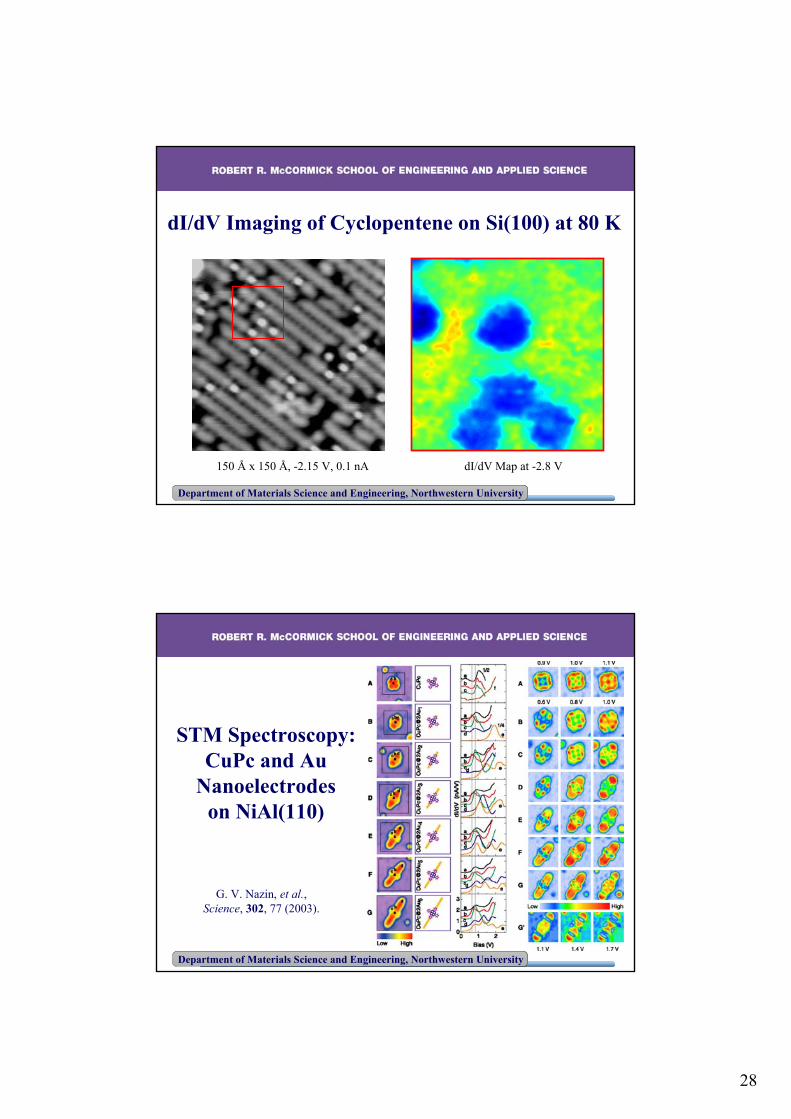
I-V Curve for TEMPO on n+-Si(100)
-0.50
-0.25
0.00
0.25
0.50
Cur
rent
(nA
)
-5.0 -2.5 0.0 2.5 5.0Voltage (V)
TEMPO on n+-Si(100)
NDR
Shoulder
-3.0
-1.5
0.0
1.5
3.0
Cur
rent
(nA
)
-5.0 -2.5 0.0 2.5 5.0Voltage (V)
Clean n+-Si(100)
• NDR events are only observed at negative sample bias. • Shoulder is only observed at positive sample bias.• NDR bias values depend sensitively on tip-sample spacing• NDR is observed in both bias sweep directions
N. P. Guisinger, et al., Nano Lett., 4, 55 (2004).
27
Department of Materials Science and Engineering, Northwestern University
TEMPO on p+-Si(100)
-3.0
-1.5
0.0
1.5
3.0
Cur
rent
(nA
)
-5.0 -2.5 0.0 2.5 5.0Voltage (V)
NDR
Shoulder
Equilibrium NDRShoulder• Qualitatively similar behavior to TEMPO on n+-Si(100) except
opposite polarity.• Orbital energy shift may be due to charge transfer with the
substrate.
I-V Curve for TEMPO on p+-Si(100)N. P. Guisinger, et al., Nano Lett., 4, 55 (2004).
Department of Materials Science and Engineering, Northwestern University
Si(100) Dosed with Cyclopentene at 80 K
2 nm
28
Department of Materials Science and Engineering, Northwestern University
150 Å x 150 Å, -2.15 V, 0.1 nA dI/dV Map at -2.8 V
dI/dV Imaging of Cyclopentene on Si(100) at 80 K
Department of Materials Science and Engineering, Northwestern University
STM Spectroscopy:CuPc and Au
Nanoelectrodeson NiAl(110)
G. V. Nazin, et al.,Science, 302, 77 (2003).
29
Department of Materials Science and Engineering, Northwestern University
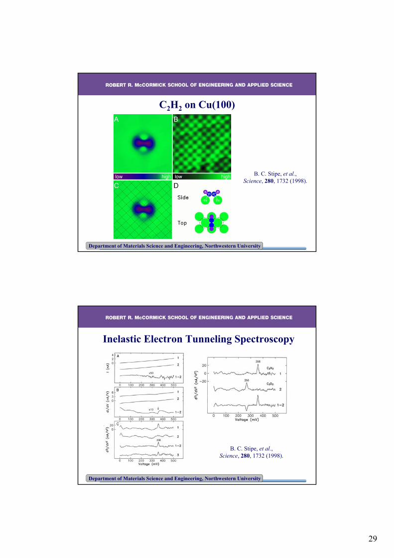
C2H2 on Cu(100)
B. C. Stipe, et al.,Science, 280, 1732 (1998).
Department of Materials Science and Engineering, Northwestern University
Inelastic Electron Tunneling Spectroscopy
B. C. Stipe, et al.,Science, 280, 1732 (1998).
30
Department of Materials Science and Engineering, Northwestern University
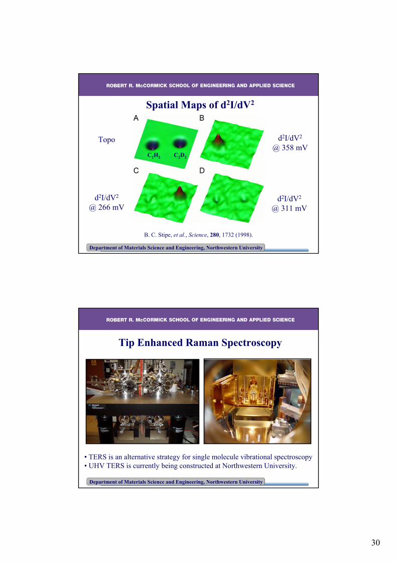
Spatial Maps of d2I/dV2
B. C. Stipe, et al., Science, 280, 1732 (1998).
Topo d2I/dV2
@ 358 mV
d2I/dV2
@ 311 mVd2I/dV2
@ 266 mV
C2H2 C2D2
Department of Materials Science and Engineering, Northwestern University
Tip Enhanced Raman Spectroscopy
• TERS is an alternative strategy for single molecule vibrational spectroscopy• UHV TERS is currently being constructed at Northwestern University.