POUR L'OBTENTION DU GRADE DE DOCTEUR ÈS SCIENCES acceptée sur proposition du jury: Prof. V. Savona, président du jury Prof. K. Kern, directeur de thèse Prof. E. Scheer, rapporteuse Prof. P. Liljeroth, rapporteur Prof. H. Brune, rapporteur Scanning Tunneling Spectroscopy with Superconducting Junctions: From Single Channel Transport to Local Pair Breaking Potentials THÈSE N O 8730 (2018) ÉCOLE POLYTECHNIQUE FÉDÉRALE DE LAUSANNE PRÉSENTÉE LE 16 JUILLET 2018 À LA FACULTÉ DES SCIENCES DE BASE LABORATOIRE DE SCIENCE À L'ÉCHELLE NANOMÉTRIQUE PROGRAMME DOCTORAL EN PHYSIQUE Suisse 2018 PAR Jacob SENKPIEL
Transcript
POUR L'OBTENTION DU GRADE DE DOCTEUR ÈS SCIENCES
acceptée sur proposition du jury:
Prof. V. Savona, président du juryProf. K. Kern, directeur de thèse
Prof. E. Scheer, rapporteuseProf. P. Liljeroth, rapporteurProf. H. Brune, rapporteur
Scanning Tunneling Spectroscopywith Superconducting Junctions:From Single Channel Transport
to Local Pair Breaking Potentials
THÈSE NO 8730 (2018)
ÉCOLE POLYTECHNIQUE FÉDÉRALE DE LAUSANNE
PRÉSENTÉE LE 16 JUILLET 2018
À LA FACULTÉ DES SCIENCES DE BASELABORATOIRE DE SCIENCE À L'ÉCHELLE NANOMÉTRIQUE
PROGRAMME DOCTORAL EN PHYSIQUE
Suisse2018
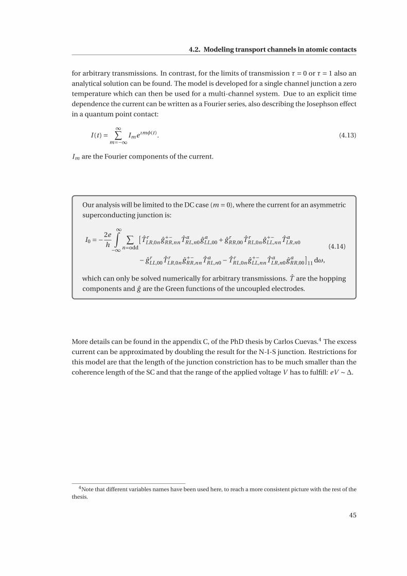
PAR
Jacob SENKPIEL
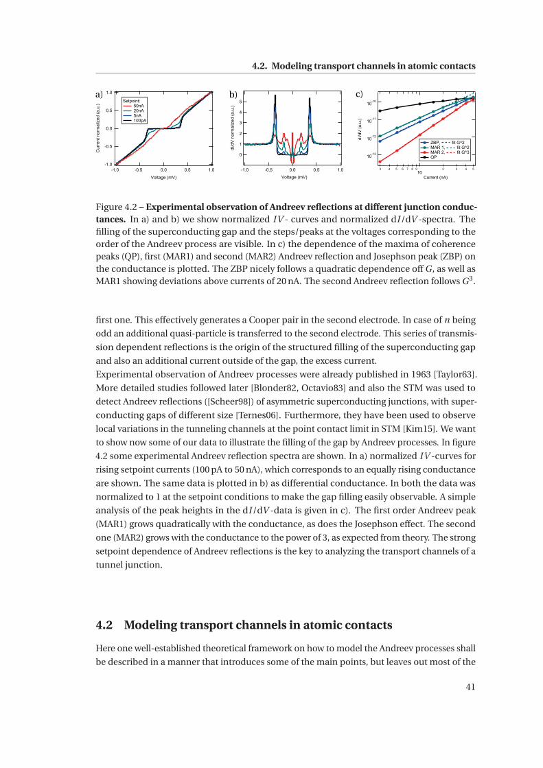
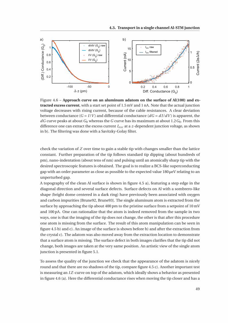
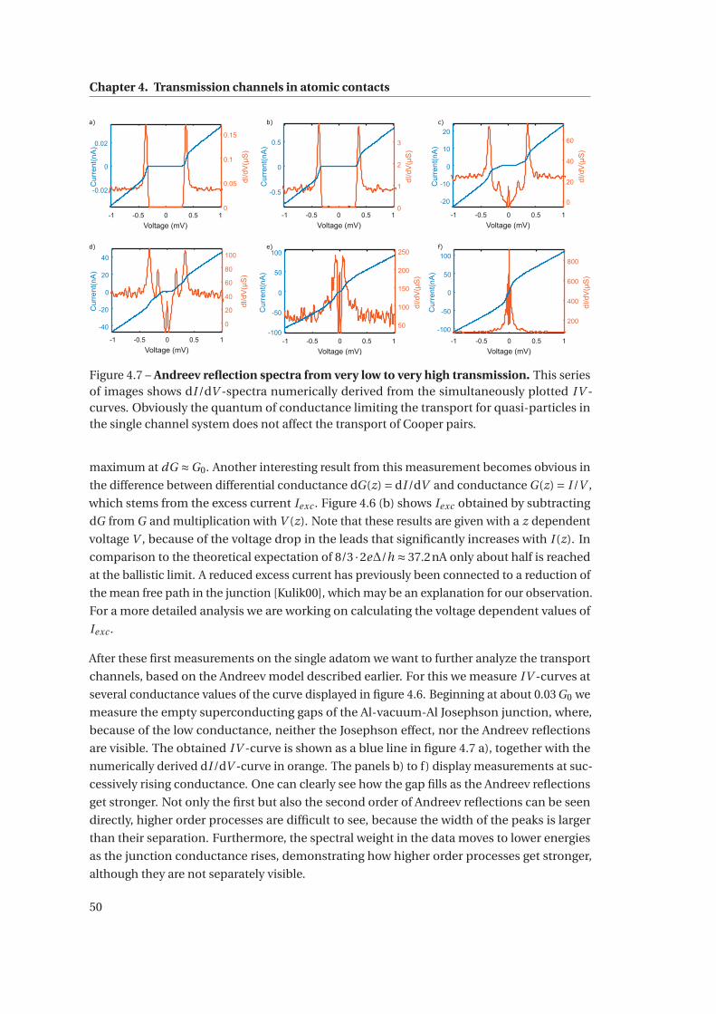
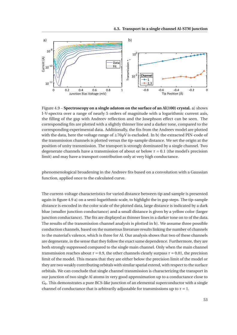
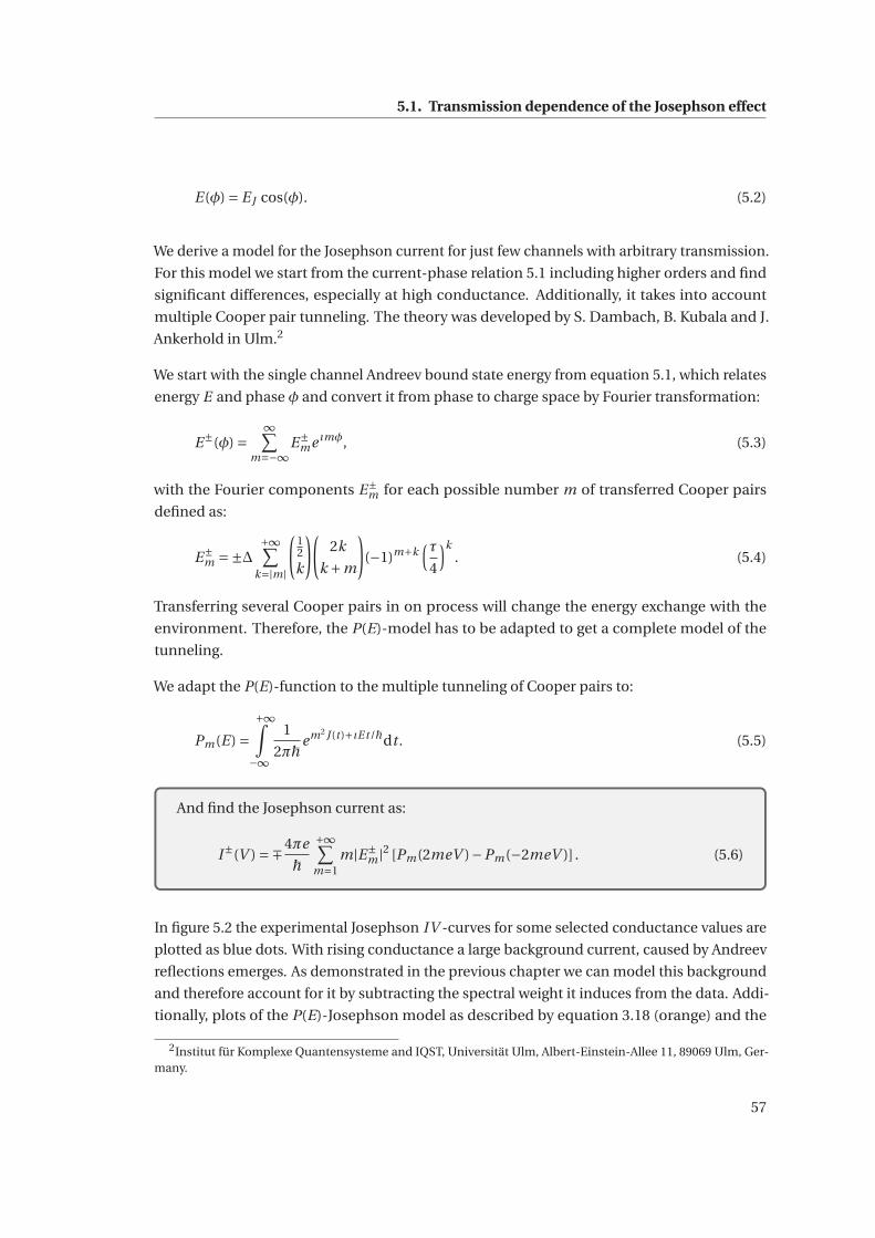
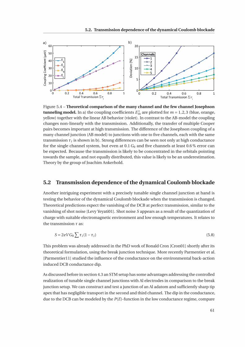
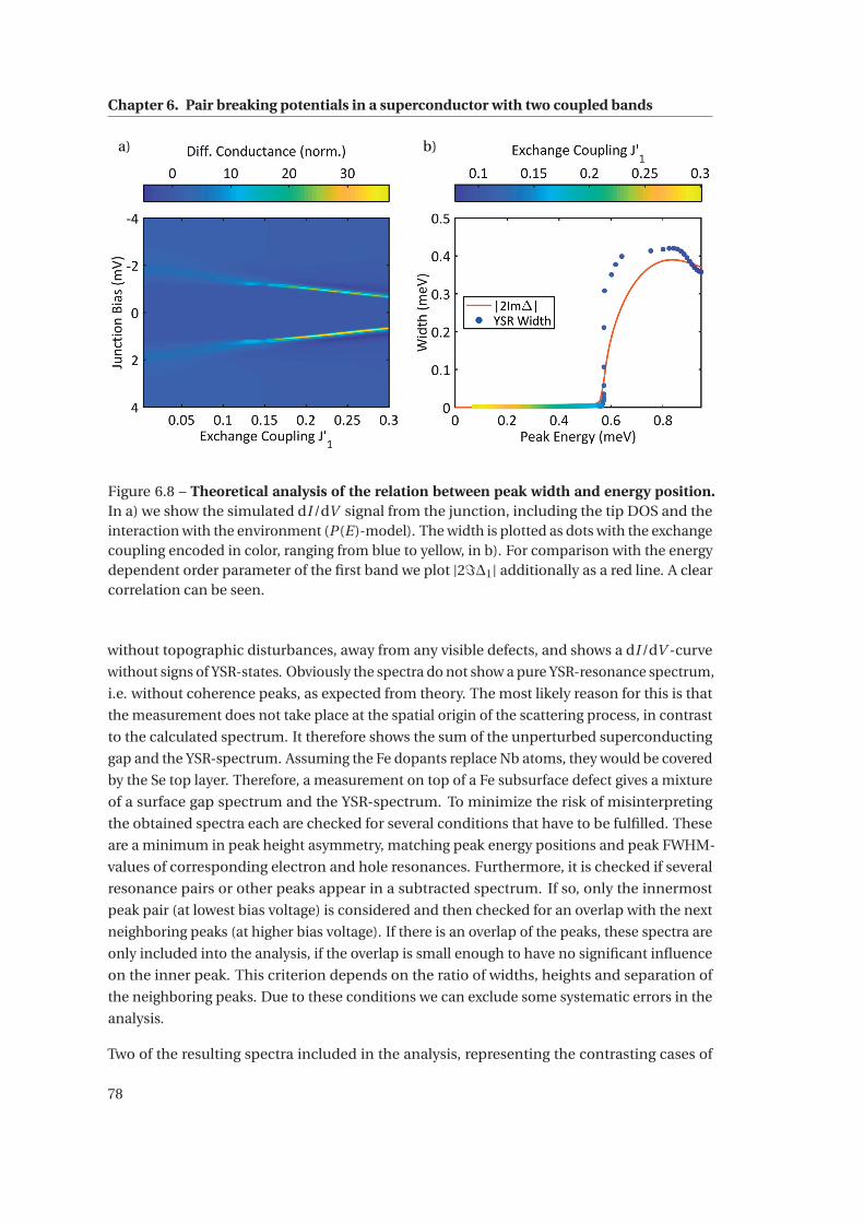
AbstractThis thesis contains two major topics, the restriction of tunneling to only a few channels in the
scanning tunneling microscope (STM) and the interaction of local magnetic impurities with
superconductivity.
At a temperature of 15 mK, the quantum back-action of the electromagnetic environment
in an STM junction becomes prominent. It influences the tunneling process, and by that
inevitably also the spectroscopy of physical phenomena. We demonstrate that the macro-
scopic tip shape strongly defines this back-action. It can be reduced by increasing the tip wire
diameter. This increases the capacitance of the junction, and thereby significantly enhances
the spectroscopic energy resolution. Modeling this effect with P(E)-theory, we extrapolate
that the electromagnetic environment of the junction influences measurements in the STM
up to a temperature of about 1 K. This result helps establish a direct correspondence between
the P(E)-model and the energy resolution function of the STM.
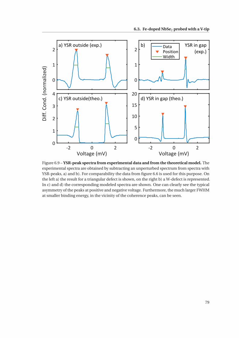
We further study the tunneling process by constructing a single channel junction made of
an Al adatom on an Al(100) crystal and the single apex atom of an Al tip. We provide proof
that the transport in this junction is strongly limited to a single channel by analyzing Andreev
reflection spectra over a wide conductance range up to the quantum of conductance.
With this junction we show how the Josephson effect deviates from the many channel and low
transmission model by Ambegaokar and Baratoff. We also present a new model, based on the
full Andreev bound state relation for the few channel limit, which accounts for transmission
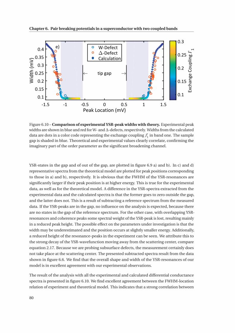
dependencies and multiple Cooper pair tunneling processes. Modeling the Josephson effect
in our junction this new model reproduces the experimental data in great detail. Regarding
the determination of the Josephson coupling energy or critical current in STM-experiments,
we expect at least 0.6 % and up to 2.6 % deviation from the linear model at a conductance of
0.1G0 and up to 17 % at 0.5G0.
In the normal conducting state of this single channel junction the environmental back-action
manifests as a transmission reduction around zero voltage, known as the dynamical Coulomb
blockade (DCB). Here we test the predicted vanishing of the DCB for transmissions towards
unity in a single channel system. Our data clearly support this expectation. These results
suggest that the transport process becomes less sensitive to the environmental back-action
with increasing channel transmission.
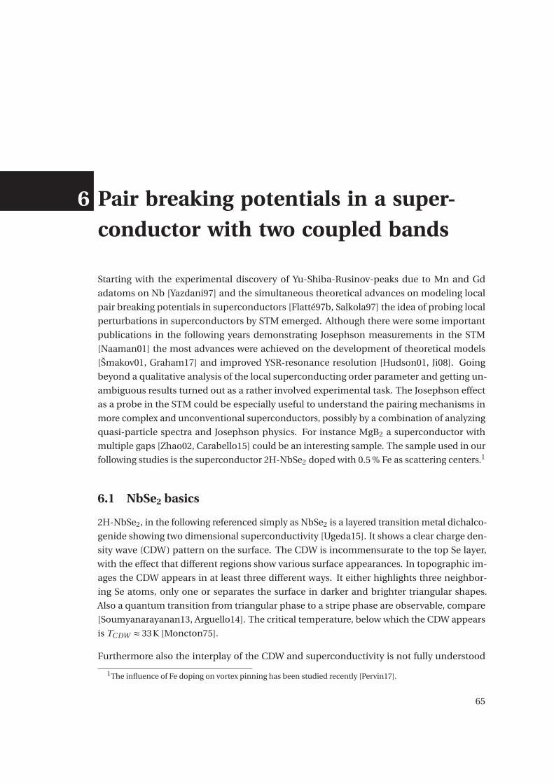
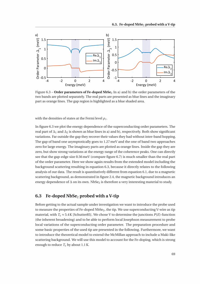
Concerning pair breaking potentials in a multi-band superconductor, we study Fe-doped
NbSe2 with a V-tip. We demonstrate that Yu-Shiba-Rusinov (YSR) resonances emerge not only
i
in the energy-gap but also outside of it, at the position of coherence peaks, where they are
significantly broadened. We demonstrate a direct correspondence of the YSR-state lifetime to
the imaginary part of the superconducting order parameter (Δ). To demonstrate this corre-
spondence we compare the experimental peak-width to peak-energy-position dependence
with a T-matrix scattering model, taking into account the two-band superconductivity of
NbSe2, with inter-band coupling and magnetic background scattering. Our results show that
YSR-resonances can be used to probe the imaginary part of the superconducting order pa-
rameter. We suspect that many asymmetries observed in spectra of the superconducting gap
are related to this effect. We collate some early results of the local Josephson critical current
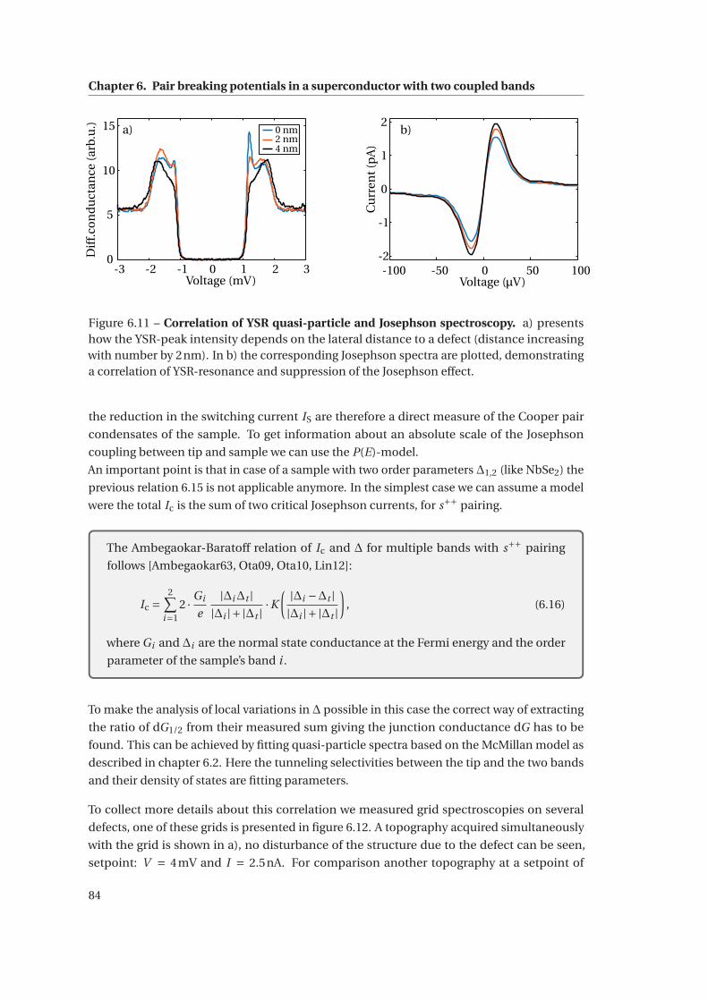
and the inferred amplitude of the superconducting order parameter in NbSe2. We find local
variations around the embedded Fe impurities suggesting that the order parameter is reduced
by about 20 %.
Key words:
Josephson scanning tunneling microscopy (JSTM)
Multi-band superconductivity
Pair-breaking potentials
Superconducting order parameter
Yu-Shiba-Rusinov states (YSR)
Andreev reflections
Single channel transmission
Quantum back-action
Dynamical Coulomb blockade (DCB)
ii
ZusammenfassungDie vorliegende Arbeit behandelt zwei Hauptthemen, die Abhängigkeit des Tunnelprozess im
Rastertunnelmikroskop (RTM) von den Transportkanälen und die Wechselwirkung lokaler
magnetischer Störer mit Supraleitern.
Bei einer Temperatur von 15 mK erlangt die Quanten-Rückwirkung der elektromagnetischen
Umgebung des Tunnelkontaktes eine erhebliche Bedeutung. Sie beeinflusst den Tunnelpro-
zess und damit unumgänglich auch spektroskopische Messungen physikalischer Phänomene.
Wir zeigen, dass insbesondere die makroskopischen Abmessungen der RTM-Spitze diese Rück-
wirkung bestimmen. Sie kann verrringert werden, indem der Durchmesser der Spitze erhöht
wird. Dies erhöht die Kapazität zwischen Spitze und Probe, was wiederum eine signifikante
Verbesserung der Energieauflösung zur Folge hat. Dieser Effekt kann mit der sogenannten
P(E)-Theorie beschrieben werden. Wir erwarten, dass er bis zu einer Temperatur von etwa 1 K
Messungen beeinflusst. Diese Ergebnisse etablieren das P(E)-Model weiter für Rastertunnel-
mikroskopie.
Des Weiteren untersuchen wir die Besonderheiten von Einkanaltunneln zwischen zwei einzel-
nen Al Atomen. Anhand von Andreev-Refletions Spekten über einen sehr großen Widerstands-
bereich bis zum Quantum der Leitfähigkeit beweisen wir, dass in sehr guter Näherung nur ein
einzelner Kanal für den Transport verantwortlich ist. Mit diesem Einkanalübergang studieren
wir die Transmissionsabhängigkeit des Josephson Effekts und wie sie von dem Model von
Ambegaokar und Baratoff (AB) für viele Kanäle abweicht. Wir benutzen ein neues Model, das
auf der vollständigen Relation für gebundene Andreev-Zustände beruht. Es ist transmissions-
abhängig und berücksichtigt simultanes Tunneln von mehreren Cooper Paaren. Wir finden
eine hervorragende Übereinstimmung zwischen unseren Daten und den Ergebnissen des
Models. Im Bezug auf die Ermittlung der Josephson Kopplung mit dem RTM zeigt unsere
Studie, dass mindestens 0.6 % und bis zu 2.6 % Abweichung von dem AB-Model, bei einer
Leitfähigkeit von 0.1G0 zu erwarten sind, bei 0.5G0 sogar bis zu 17 %.
Im normalleitenden Zustand des Tunnelübergangs wird die Rückwirkung der Umgebung
direkt in Form der dynamischen Coulomb Blockade (DCB) sichtbar. Es wird erwartet, dass sie
bei steigender Transmission τ kleiner wird und bei τ= 1 verschwindet. Unsere experimellen
Daten sind in Übereinstimmung mit dieser Erwartung. Dieses Ergebniss suggeriert, dass der
Transport mit steigender Transmission weniger empfänglich für die Rückwirkung der Umge-
bung wird.
Im Bezug auf paarbrechende Potentiale in Supraleitern haben wir Fe dotiertes NbSe2 un-
tersucht. Wir haben demonstriert, dass Yu-Shiba-Rusinov (YSR) Resonanzen nicht nur in
iii
der Bandlücke von Supraleitern existieren können, sondern auch außerhalb. Wir finden sie
auch in dem Energiebereich der Koheränzmaxima, wo sie eine erheblich größere Breite auf-
weisen. Wir können eine direkte Abhängigheit zwischen der Lebensdauer der YSR-Zustände
und dem imaginären Teil des supraleitenden Ordnungsparameters zeigen. Um diesen zu
beweisen vergleichen wir den experimentellen Zusammenhang von Resonanzposition und
Breite mit einem theoretischen Model auf Basis von T-Matrix Streuungk. In diesem werden
Inter-Bandkopplung und Streuung an einem magnetischen Hintergrund berücksichtigt. Unse-
re Ergebnisse zeigen, dass YSR-Resonanzen dazu verwendet werden können den imaginären
Teil des supraleitenden Ordnungsparameters zu erfassen. Oft beobachtete Asymmetrien in
den Koherenzmaxima von Supraleitern könnten von diesem Phänomen herrühren. Wir zeigen
außerdem eine erste Analyse der Variationen des kritischen Josephson Stromes in NbSe2.
Unsere Daten lassen eine lokale Änderung des supraleitenden Ordnungsparameters um 20 %
in der Umgebung der Fe Defekte erwarten.
Stichwörter:
Josephson-Rastertunnelmikroskopie (JRTM)
Multiband-Supraleitung
Paarbrechende Potentiale
Supraleitender Ordnungsparameter
Yu-Shiba-Rusinov Zustände
Andreev-Refletionen
Einkanaltransmission
Quanten-Rückwirkung
Dynamische Coulomb Blockade (DCB)
iv
AcknowledgementsBefore starting the scientific part I want to express my gratitude to the people that were in-
volved in achieving the presented work or participated in other ways that made this thesis
possible.
First of all I want to thank Klaus Kern for accepting me as a PhD student in his group and
providing an excellent working environment with lots of freedom. I have the deepest respect
for him and the scientific achievements he realized here at the MPI in Stuttgart.
I am grateful to Christian Ast and Markus Etzkorn, who guided me through my work as a PhD
student. Also their proofreading of this thesis was certainly important to reach its final stage. I
really enjoyed working together with them. The many hours in the lab and also discussing
physics were not only highly educational for me but also a lot of fun.
I want to express my gratitude to the members of my thesis committee; Vincenzo Savona,
Harald Brune, Elke Scheer and Peter Liljeroth for taking the time to review my PhD studies.
I want to thank Carmen Rubio Verdú for the time we shared together working at Box 1 on
science stuffs. It was a truly awesome time.
Berthold Jäck and Matthias Eltschka have my sincere thanks for introducing me to the ways of
the machine and paving the way for my work. I want to especially acknowledge Bert for the
fruitful work on our joint publications.
Joachim Ankerhold has my gratitude for the various enlightening meetings and the fruitful
collaboration.
Inspiring discussions with Alexander Balatsky, Francesco Tafuri, Fabien Portier, Carlos Cuevas,
Annica Black-Schaffer, Wolfgang Beltzig, Andreas Rost, Markus Ternes, Jochen Mannhart,
Hans Boschker, Jurgen Smet helped a lot in developing my understanding of the different
topics that emerged during my studies.
I thank the many people, who made the work possible: Wolfgang Stiepany, Peter Andler, Marco
Memmler, our IT-department, the electronics-group, the low temperature service and more.
v
Acknowledgements
The general conditions and friendly atmosphere at the institute, ranging from the staff helping
with travel forms to the security guards were outstanding.
I am grateful to Christopher Leon for proofreading parts of this thesis.
A special thanks to my office and PL buddies, colleagues and friends: Shai Mangel, Rico Gutzler,
Diana Hoetger, Robert Drost, Anna Roslawska, Tomasz Michnowicz, Haonan Huang, Andreas
Topp, Christopher Leon, Bastian Kern, Abhishek Grewal, Piotr Kot, Sebastian Koslowski, Chris-
tian Dette, Sabine Abb, Verena Schendel and many more for a great time at the MPI.
I am grateful to Sabine Birtel for keeping control over all organizational problems.
Matthias Bode and Jens Kügel have my thanks, because I got part of my motivation to start a
PhD on the mK-STM in the time I spend in Matthias’ group during my master studies.
I thank my parents for supporting me on my way through life.
The most significant and personally important support came from my partner Katharina,
who always had my back and enabled me to spend way too much time with this thesis. I am
thankful to our daughter for cheering me up and helping me to forget, whatever imaginary
problem was sitting on my mind and for our joint bike trips to and from work, which kept me
Heinrich18, Kezilebieke18] and their connection to the attempts to demonstrate Majorana
bound states [Potter12, Das12, Nadj-Perge14, Feldman16, Ruby15b, Lv17, Jeon17] attracted a
lot of attention in the last years. We contribute to this field by demonstrating the emergence of
YSR-resonances outside of the superconducting gap, at the position of the coherence peaks,
1Unisoku USM1300.
1
Chapter 1. Introduction
and connect their lifetime to the imaginary part of the underlying superconducting substrate.
By this it is possible to determine to what amount states residing inside the gap are protected
against relaxation [Heinrich13] and it may help to find the best suited environment to realize
long-lived quantum states necessary for quantum sensing, computation and simulation
[Suter16]. Including the possibility of YSR-resonances at the position of the coherence peaks
may account for ofttimes observed asymmetries in superconducting gaps.
The recently discovered unconventional superconductivity in sheets of graphene rotated by an
angle of about 1.1 ° [Cao18] is quite interesting because it consists of only one element, much
unlike most other SC with unconventional pairing. To study this material and to find clues
on the details of the pairing mechanism Josephson scanning tunneling microscopy (JSTM)
[Šmakov01, Graham17] may be the ideal tool [Jäck15b, Jäck15a, Randeria16].
This thesis is structured in the following way. It begins with a short description of the relevant
physical phenomena in chapter 2. After that the experiment and its important characteristics
are explained in chapter 3. We then elaborate on our findings concerning the tunneling
process in a single channel junction in chapters 4 and 5, where we study the Josephson effect
and the dynamical Coulomb blockade. The last chapter (6) is concerned with the interaction
of local magnetic moments with a superconductor with two coupled bands.
2
2 Tunneling between superconductors
In this first part the thesis we will introduce some physics important for the understanding of
the experimental work to follow. All explanations will be on a basic level, possibly restricted
to giving a phenomenological idea. In case there is interest for further reading there shall be
some recommendations in the text. We will start with introducing the principle of tunneling
measurements, leading to the scanning tunneling microscope. After that, the most relevant
properties of superconductivity are noted down together with their experimental signatures.
Then local perturbations of SC will be discussed, leading to Yu-Shiba-Rusinov-resonances
and spatial variations of the pairing amplitude of the superconducting order parameter. After
that the Josephson-effect, describing the transport of Cooper pairs between superconducting
reservoirs, will be introduced. At the end of this chapter the Josephson-effect as a means to
probe local changes of the superconducting order parameter in the STM, will be highlighted.
2.1 Tunneling and scanning tunneling microscopy
2.1.1 The concept of tunneling particles
The concept of tunneling particles goes back to the work of Louis de Broglie1 who in 1923
proposed the duality of particle and wave nature of matter [Broglie23]. Following this concept
one can assign a wavelength λ to a particle with mass m and speed v :
λ= h
mv, (2.1)
where h is Planck’s constant. h as link of a photon’s energy E and frequency ν was proposed
by Max Planck2 in 1900 to satisfy E = hν [Planck00] and is contained in the explanation of the
1De Broglie was awarded the Nobel price in Physics 1929: “for his discovery of the wave nature of electrons”[Nobel Media AB18].
2Planck was awarded the Nobel price in Physics 1918: “in recognition of the services he rendered to theadvancement of Physics by his discovery of energy quanta” [Nobel Media AB18].
3
Chapter 2. Tunneling between superconductors
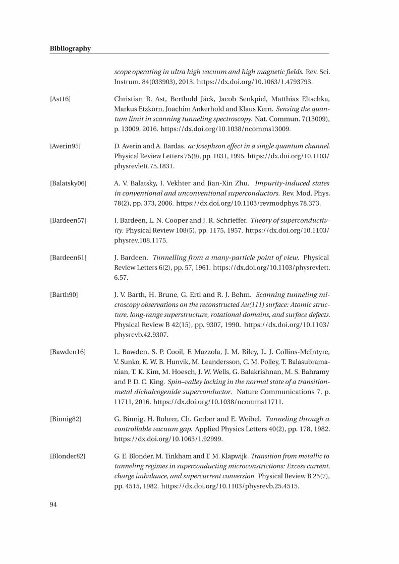
0 d
E
z
EF
V = 0
0 d
E
z
V > 0
0 d
E
z
V < 0
EF
EF
eV
eV
(Tip) (Sample)
ρL
ρR
a) b) c)
WL WREF
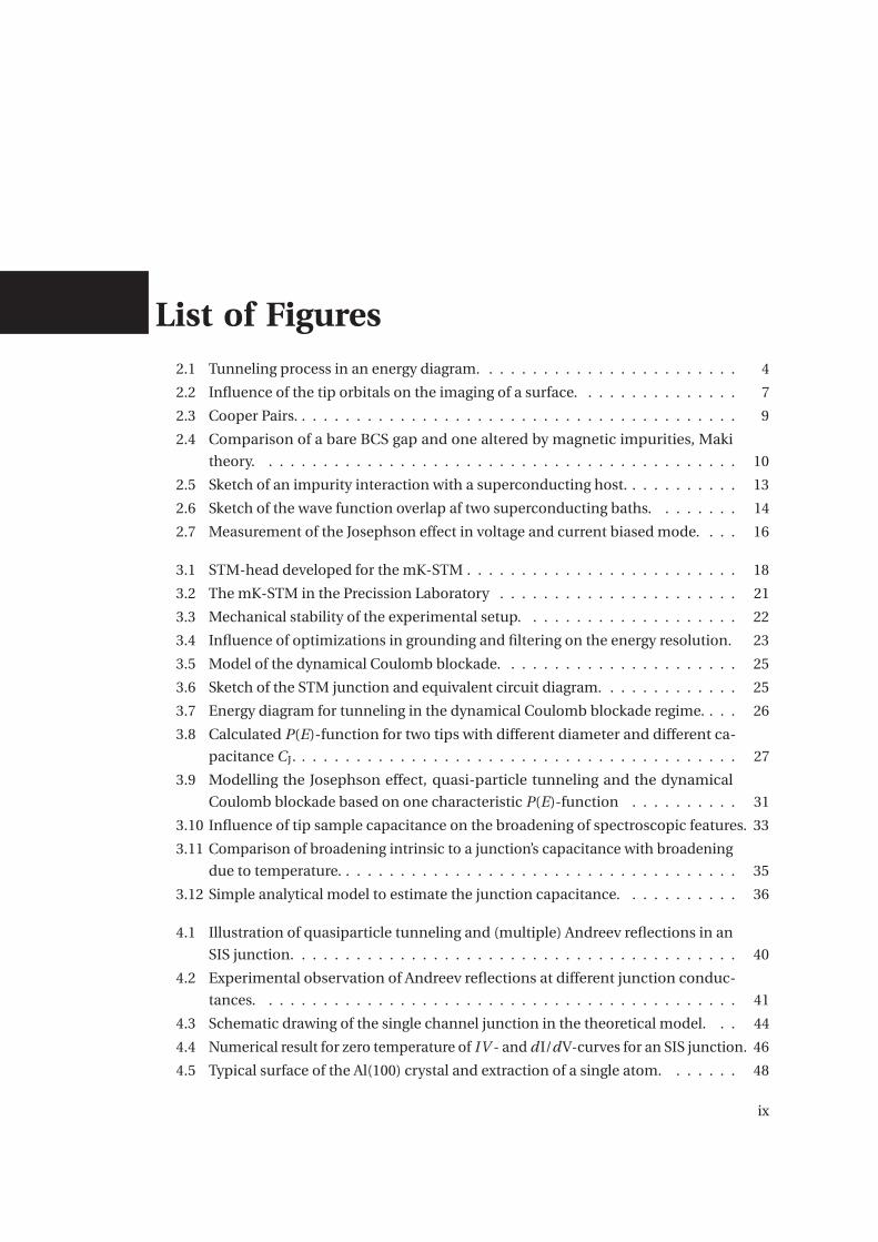
EF
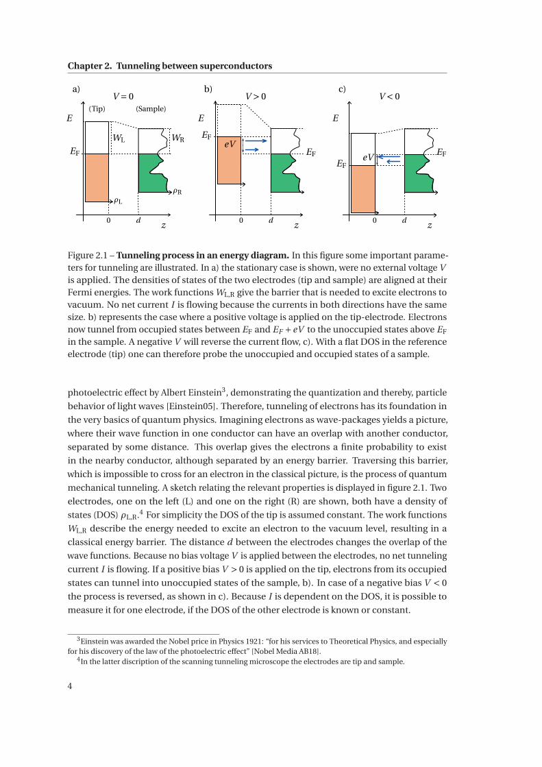
Figure 2.1 – Tunneling process in an energy diagram. In this figure some important parame-ters for tunneling are illustrated. In a) the stationary case is shown, were no external voltage Vis applied. The densities of states of the two electrodes (tip and sample) are aligned at theirFermi energies. The work functions WL,R give the barrier that is needed to excite electrons tovacuum. No net current I is flowing because the currents in both directions have the samesize. b) represents the case where a positive voltage is applied on the tip-electrode. Electronsnow tunnel from occupied states between EF and EF +eV to the unoccupied states above EF
in the sample. A negative V will reverse the current flow, c). With a flat DOS in the referenceelectrode (tip) one can therefore probe the unoccupied and occupied states of a sample.
photoelectric effect by Albert Einstein3, demonstrating the quantization and thereby, particle
behavior of light waves [Einstein05]. Therefore, tunneling of electrons has its foundation in
the very basics of quantum physics. Imagining electrons as wave-packages yields a picture,
where their wave function in one conductor can have an overlap with another conductor,
separated by some distance. This overlap gives the electrons a finite probability to exist
in the nearby conductor, although separated by an energy barrier. Traversing this barrier,
which is impossible to cross for an electron in the classical picture, is the process of quantum
mechanical tunneling. A sketch relating the relevant properties is displayed in figure 2.1. Two
electrodes, one on the left (L) and one on the right (R) are shown, both have a density of
states (DOS) ρL,R.4 For simplicity the DOS of the tip is assumed constant. The work functions
WL,R describe the energy needed to excite an electron to the vacuum level, resulting in a
classical energy barrier. The distance d between the electrodes changes the overlap of the
wave functions. Because no bias voltage V is applied between the electrodes, no net tunneling
current I is flowing. If a positive bias V > 0 is applied on the tip, electrons from its occupied
states can tunnel into unoccupied states of the sample, b). In case of a negative bias V < 0
the process is reversed, as shown in c). Because I is dependent on the DOS, it is possible to
measure it for one electrode, if the DOS of the other electrode is known or constant.
3Einstein was awarded the Nobel price in Physics 1921: “for his services to Theoretical Physics, and especiallyfor his discovery of the law of the photoelectric effect” [Nobel Media AB18].
4In the latter discription of the scanning tunneling microscope the electrodes are tip and sample.
4
2.1. Tunneling and scanning tunneling microscopy
A possible basis for the theoretical analysis of the tunneling current is found in the work of
Erwin Schrödinger5 who developed the framework to describe the time evolution of a system’s
wave function [Schrödinger26]. This framework was used by John Bardeen6 to derive an
equation for the tunneling current I in the one-dimensional case [Bardeen61]. By simplifying
the problem with several assumptions7 the tunneling current I can be derived from the overlap
of the electrodes wave functions [Chen07]:
I (V ) = 4πe
ħ
∞∫−∞
[ f (EF −eV +ε)− f (EF +ε)]×ρL(EF −eV +ε)ρR (EF +ε)|M |2 dε, (2.2)
with the tunneling matrix element M and the Fermi distribution, describing the temperature
dependent smearing of the DOS:
f (E) = 1
1+exp(
E−EFkB T
) . (2.3)
The influence of the specific materials used as electrodes as well as the distance between
them enters |M |. The wave functions are represented by the decay constant κ0 of the averaged
work-function and the work functions by WL,R.
M(ε) = M(0) ·e
κ0εd
WL +WR , (2.4)
where d is the separation of the two electrodes. If the broadening of spectroscopic features
is not significant (because of a low enough temperature) one may ignore the Fermi function.
Additionally, assuming a constant tunneling matrix element |M | over the energy range of
interest, one gets the simple relation:
I (V ) ∝eV∫0
ρL(EF −eV +ε)ρR (EF +ε)dε. (2.5)
Clearly, a measured current follows from the convolution of the two electrode’s densities of
states. And the differential conductance signal is directly proportional to the convolution of
the electrodes densities of states:
dG(V ) =(
dI
dU
)U=V
≈ ρL(EF +eV )ρR (EF ). (2.6)
Obtaining the structure of the density of states in a tunneling experiment was achieved by Leo
5Schrödinger was awarded the Nobel price in Physics 1933: “for the discovery of new productive forms of atomictheory” [Nobel Media AB18].
6Bardeen was awarded the Nobel prize in physics 1956 together with William Shockley and Walter Brattain: “fortheir researches on semiconductors and their discovery of the transistor effect” [Nobel Media AB18].
7The simplifications are given by assuming: orthogonal tip and sample states, weak tunneling, electron-electroninteractions can be ignored, independent tip and sample DOS unaltered by the tunneling and electrochemicalequilibrium between tip and sample [Gottlieb06]
5
Chapter 2. Tunneling between superconductors
Esaki8 and P.J. Stiles in 1965 [Esaki65].
Another possibility to look at the tunneling process is based on conduction channels between
the electrodes, each supporting a maximal current at a certain voltage, defined by the quantum
of conductance G0 = 2e2
πh , with h being the Planck constant. According to the Landauer theory,
the tunneling process between several states in each electrode can be split in pairs with one
state in each electrode, yielding one transport channel each [Landauer87, Chen07]. In the
tunneling regime the conductance is then given by the sum of the transmission coefficients
TN ∝ ρLρR ranging between 0 and 1 over all N channels:
G =G0∑N
TN . (2.7)
An experimental signature of the quantized transport channels is the integer Quantum Hall
effect demonstrated by Klaus von Klitzing [Klitzing80]9. Another demonstration is the trans-
port in quantum point contacts [van Wees88, Wharam88]. We will get back to the idea of
transmission channels later in chapter 4, where it will be necessary to describe the Josephson
effect in the few channel limit in our experiment.
2.1.2 Scanning tunneling microscopy
Scanning tunneling microscopy adds some very useful options to tunneling experiments.
The most obvious and renown capability is probably the imaging of surfaces with atomic
precision, based on the exponential dependence of tunneling current I and distance between
the electrodes d . Another is the manipulation of single atoms or molecules on the surface.
The electrodes in the scanning tunneling microscope (STM) are a conducting sample and a
conducting wire with an atomically sharp apex, the tip.
Control over the distance d , as well as the lateral position of the tip with respect to the sample
is realized by piezoelectric motors and actuators, adding some complexity to the experimental
setup. After the invention of the STM by Gerd Binnig and Heinrich Rohrer10 in 1982 [Binnig82]
STM quickly evolved to a powerful measurement technique, not only to image surfaces but
also for (local) spectroscopic analysis of electronic material properties. The details of the
tunneling process was studied by Tersoff and Hamann [Tersoff83, Tersoff85] who found in 1983
a quantitative theoretical description using a spherical tip, finding that STM images the local
density of states (DOS). They used Bardeen’s approach and included the tip with a spherical
potential originating in a point, without any geometric features, significantly simplifying the
description of the tips states. The most important result is that the STM measures the DOS of
the sample in a local fashion, instead of the atomic structure directly, assuming a constant tip
8Esaki was awarded the Nobel price in Physics 1973 (together with Giaever and Josephson): “for their ex-perimental discoveries regarding tunneling phenomena in semiconductors and superconductors, respectively”[Nobel Media AB18].
9Von Klitzing was awarded the Nobel prize in physics 1985: “for the discovery of the quantized Hall effect”[Nobel Media AB18].
10Rohrer and Binnig were awarded the Nobel price in Physics 1986: “for their design of the scanning tunnelingmicroscope” [Nobel Media AB18].
6
2.1. Tunneling and scanning tunneling microscopy
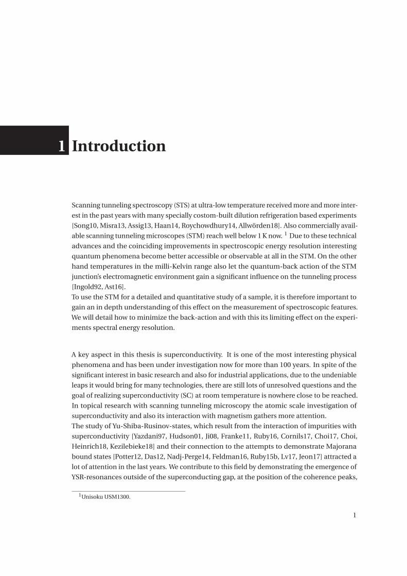
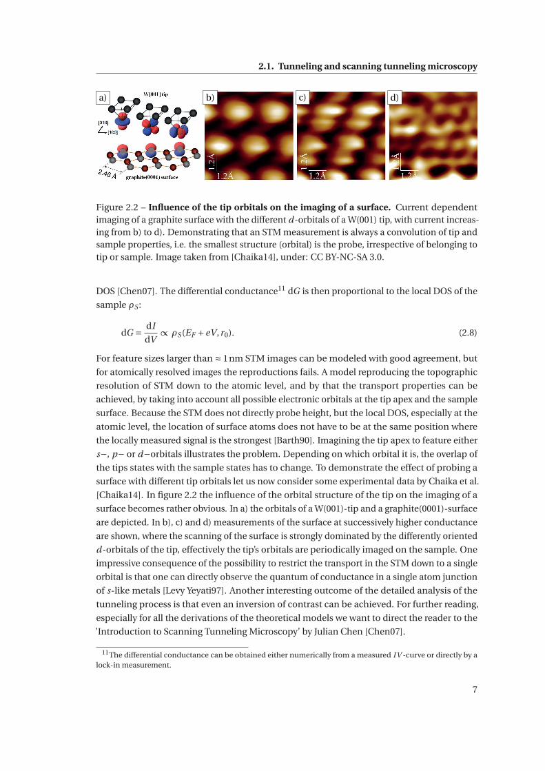
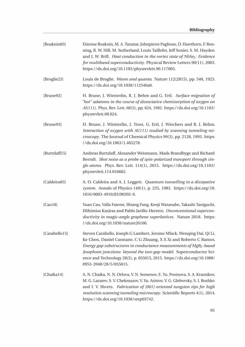
a) b) c) d)
Figure 2.2 – Influence of the tip orbitals on the imaging of a surface. Current dependentimaging of a graphite surface with the different d-orbitals of a W(001) tip, with current increas-ing from b) to d). Demonstrating that an STM measurement is always a convolution of tip andsample properties, i.e. the smallest structure (orbital) is the probe, irrespective of belonging totip or sample. Image taken from [Chaika14], under: CC BY-NC-SA 3.0.
DOS [Chen07]. The differential conductance11 dG is then proportional to the local DOS of the
sample ρS :
dG = dI
dV∝ ρS(EF +eV ,r0). (2.8)
For feature sizes larger than ≈ 1nm STM images can be modeled with good agreement, but
for atomically resolved images the reproductions fails. A model reproducing the topographic
resolution of STM down to the atomic level, and by that the transport properties can be
achieved, by taking into account all possible electronic orbitals at the tip apex and the sample
surface. Because the STM does not directly probe height, but the local DOS, especially at the
atomic level, the location of surface atoms does not have to be at the same position where
the locally measured signal is the strongest [Barth90]. Imagining the tip apex to feature either
s−, p− or d−orbitals illustrates the problem. Depending on which orbital it is, the overlap of
the tips states with the sample states has to change. To demonstrate the effect of probing a
surface with different tip orbitals let us now consider some experimental data by Chaika et al.
[Chaika14]. In figure 2.2 the influence of the orbital structure of the tip on the imaging of a
surface becomes rather obvious. In a) the orbitals of a W(001)-tip and a graphite(0001)-surface
are depicted. In b), c) and d) measurements of the surface at successively higher conductance
are shown, where the scanning of the surface is strongly dominated by the differently oriented
d-orbitals of the tip, effectively the tip’s orbitals are periodically imaged on the sample. One
impressive consequence of the possibility to restrict the transport in the STM down to a single
orbital is that one can directly observe the quantum of conductance in a single atom junction
of s-like metals [Levy Yeyati97]. Another interesting outcome of the detailed analysis of the
tunneling process is that even an inversion of contrast can be achieved. For further reading,
especially for all the derivations of the theoretical models we want to direct the reader to the
’Introduction to Scanning Tunneling Microscopy’ by Julian Chen [Chen07].
11The differential conductance can be obtained either numerically from a measured IV -curve or directly by alock-in measurement.
7
Chapter 2. Tunneling between superconductors
A difficulty with planar junctions is that the measurements average over some area, possibly
including defects, which alter the results, i.e. early Tedrow-Meservey-Fulde experiments
[Meservey70, Tedrow71, Meservey94]. In the STM on the other hand, one can precisely choose,
to either measure far away from a defect to obtain cleaner result of the substrate properties or,
which may even be more interesting, go on purpose to the location of a defect to look at the
interactions changing the substrate’s properties.
2.2 Superconductivity
The phenomenon of vanishing resistance, known as superconductivity, was discovered in 1911
by Heike Kamerlingh Onnes12. Superconductivity (SC) is actually not limited to dissipationless
conduction of electricity but also includes a transition to perfect diamagnetism, expelling
magnetic fields, an effect discovered by and named after Walther Meißner and Robert Ochsen-
feld [Meissner33]. A first microscopic description of the effect was developed by John Bardeen,
Leon Neil Cooper and John Robert Schrieffer13, the BCS-model [Bardeen57]. Its underlying
idea is that electrons bind together to pairs, the so-called Cooper pairs, and condense into
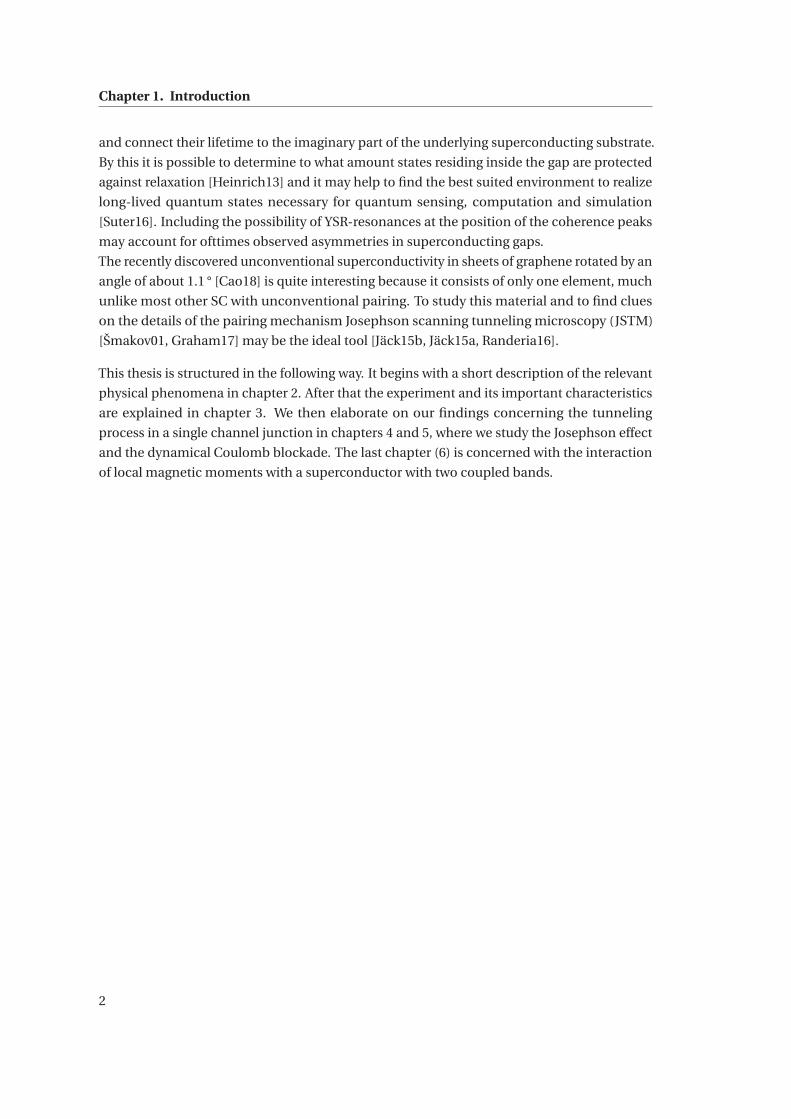
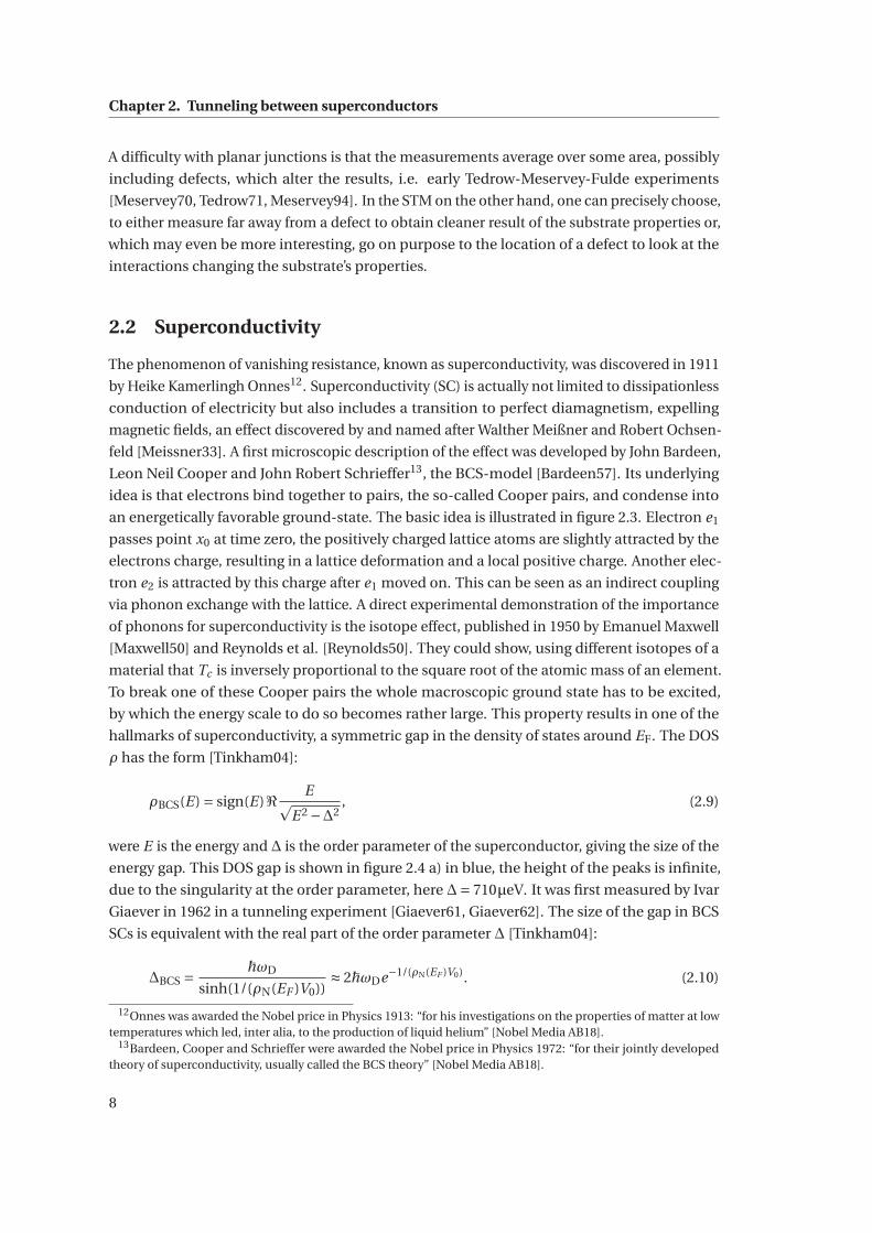
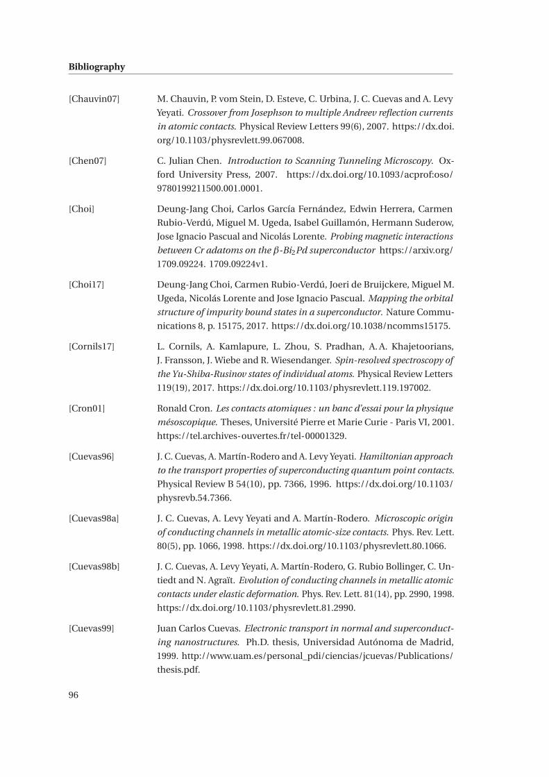
an energetically favorable ground-state. The basic idea is illustrated in figure 2.3. Electron e1
passes point x0 at time zero, the positively charged lattice atoms are slightly attracted by the
electrons charge, resulting in a lattice deformation and a local positive charge. Another elec-
tron e2 is attracted by this charge after e1 moved on. This can be seen as an indirect coupling
via phonon exchange with the lattice. A direct experimental demonstration of the importance
of phonons for superconductivity is the isotope effect, published in 1950 by Emanuel Maxwell
[Maxwell50] and Reynolds et al. [Reynolds50]. They could show, using different isotopes of a
material that Tc is inversely proportional to the square root of the atomic mass of an element.
To break one of these Cooper pairs the whole macroscopic ground state has to be excited,
by which the energy scale to do so becomes rather large. This property results in one of the
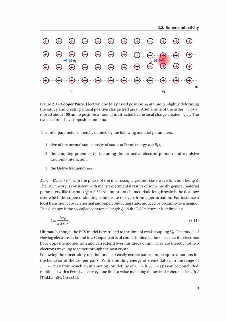
hallmarks of superconductivity, a symmetric gap in the density of states around EF. The DOS
ρ has the form [Tinkham04]:
ρBCS(E) = sign(E)ℜ E�E 2 −Δ2
, (2.9)
were E is the energy and Δ is the order parameter of the superconductor, giving the size of the
energy gap. This DOS gap is shown in figure 2.4 a) in blue, the height of the peaks is infinite,
due to the singularity at the order parameter, here Δ= 710μeV. It was first measured by Ivar
Giaever in 1962 in a tunneling experiment [Giaever61, Giaever62]. The size of the gap in BCS
SCs is equivalent with the real part of the order parameter Δ [Tinkham04]:
ΔBCS = ħωD
sinh(1/(ρN(EF )V0))≈ 2ħωDe−1/(ρN(EF )V0). (2.10)
12Onnes was awarded the Nobel price in Physics 1913: “for his investigations on the properties of matter at lowtemperatures which led, inter alia, to the production of liquid helium” [Nobel Media AB18].
13Bardeen, Cooper and Schrieffer were awarded the Nobel price in Physics 1972: “for their jointly developedtheory of superconductivity, usually called the BCS theory” [Nobel Media AB18].
8
2.2. Superconductivity
e1 e2
x0x1
Figure 2.3 – Cooper Pairs. Electron one (e1) passed position x0 at time t0, slightly deformingthe lattice and creating a local positive charge (red area). After a time of the order ≈ 1ps e1
moved about 100 nm to position x1 and e2 is attracted by the local charge created by e1. Thetwo electrons have opposite momenta.
The order parameter is thereby defined by the following material parameters:
1. size of the normal state density of states at Fermi energy ρN (EF),
2. the coupling potential V0, including the attractive electron-phonon and repulsive
Coulomb interaction,
3. the Debye frequency ωD.
ΔBCS = |ΔBCS| · eiφ with the phase of the macroscopic ground-state wave function being φ.
The BCS theory is consistent with many experimental results of some mostly general material
parameters, like the ratio 2ΔTc
= 3.53. An important characteristic length scale is the distance
over which the superconducting condensate recovers from a perturbation. For instance a
local transition between normal and superconducting state, induced by proximity to a magnet.
This distance is the so-called coherence length ξ. In the BCS picture it is defined as:
ξ≡ ħνF
πΔT=0. (2.11)
Ultimately though the BCS model is restricted to the limit of weak coupling V0. The model of
viewing electrons as bound in a Cooper pair is of course limited in the sense that the electrons
have opposite momentum and can extend over hundreds of nm. They are thereby not two
electrons traveling together through the host crystal.
Following the uncertainty relation one can easily extract some simple approximations for
the behavior of the Cooper pairs. With a binding energy of elemental SC in the range of
ECP ≈ 1meV from which an interaction- or lifetime of τCP = ħ/ECP ≈ 1ps can be concluded,
multiplied with a Fermi velocity vF, one finds a value matching the scale of coherence length ξ
[Tinkham04, Gross12].
9
Chapter 2. Tunneling between superconductors
-1 0 1Energy (meV)
0
2
4
6
8
10
12
Den
sity
of S
tate
s BCSMaki
-1 0 1Energy (meV)
0
200
400
600
Ene
rgy
(μeV
)
Re(OPMaki
)
Im(OPMaki
)
0.4 0.6 0.8 1Energy (meV)
0
2
4
6
8
Den
sity
of S
tate
s BCSMaki
a) b) c)
(EF)
Figure 2.4 – Comparison of a bare BCS gap and one altered by magnetic impurities, Makitheory. While in the bare case, at zero temperature, the gap-edge, the coherence peak maxi-mum and the order parameter Δ are at the same energy, their values differ when impurities areinduced, as modeled with the Maki theory. In a) the density of states of a BCS gap of 710μeVis plotted in blue together with the density of states of a Maki gap in orange, one can see theinfluence of the background of magnetic impurities on the quasi-particle spectrum. The MakiDOS has the dimensionless parameter ζ=0.042. In b) the order parameter corresponding tothe Maki model is plotted. The real part of the order parameter resembles its magnitude, itis not constant anymore as for the simple BCS case (black line). The value at zero voltage,which has to be used in the Josephson effect for instance, is significantly reduced (black arrow).In c) a zoom of the DOS is shown to highlight the differences between gap-edge at 577μeV(circle), the coherence peak maximum at 722μeV (rectangle) and the actual order parameterat 677μeV (arrow) in the perturbed DOS.
Some extensions used in this work: To introduce a broadening of the DOS the so called
Dynes parameter Γ can be implemented E → E + ıΓ, making the energy complex [Dynes78].
The imaginary part of this phenomenological model introduces a finite quasi-particle lifetime
inside the gap. Consequences of this will be investigated in chapter 6.3.1.
An important possibility to adapt the BCS theory to superconductors with some macroscopic
magnetic alteration, due to magnetic impurities, is the Maki model [Maki64, Worledge00].
The quasi-particle DOS of a superconductor in the Maki model, neglecting magnetic fields
follows [Tinkham04]:
ρMaki(E) = sign(E)ℜ(
u�u2 −1
), u = E
ΔBCS+ ζu�
1−u2(2.12)
ΔBCS is the unperturbed order parameter and ζ is the depairing parameter. The now energy
dependent order parameter is given by:
ΔMaki(E) =ΔBCS −ζΔMaki(E)√
Δ2Maki(E)−E 2
. (2.13)
The Maki density of states with a large but realistic depairing parameter, is plotted together
with the BCS DOS in figure 2.4 a), showing the significant effect of magnetic scattering in
bulk SC. In addition to altering the DOS, the depairing also renders the order parameter
energy dependent, as demonstrated in b). Using ΔBCS = 710μeV and a depairing ζ= 0.042 as
10
2.2. Superconductivity
input parameters the resulting order parameter at the Fermi energy is reduced to Δ(EF )Maki =677μeV. In c) we take a closer look at the difference of the gap-edge, the coherence peak
maximum and the value of the order parameter. While these entities are at the same energy
for a BCS-like DOS and thereby make the order parameter easily accessible, this is not true
anymore for a Maki-like DOS.
A tunneling effect closely related to superconductivity is the filling of the gap upon increasing
tunneling conductance. We will study responsible process, Andreev reflection in chapter 4.
2.2.1 Local pair breaking potentials – Yu-Shiba-Rusinov states
The interaction of a local pair breaking potential, for instance due to a magnetic moment, with
a superconductor was described by Luh Yu, Hiroyuki Shiba and A.I. Rusinov [Yu65, Shiba68,
Rusinov69a], in the following abbreviated as YSR. Later more advanced theory concerned
with the local effects of impurities on superconductivity [Salkola97, Flatté97b, Flatté97a] was
developed, introducing the phenomenon as an ideal field to study by STM. Early experimantal
STM work on YSR interactions was done by Ali Yazdani et al. in 1997 [Yazdani97] followed
for instance by E. W. Hudson in 2001 [Hudson01] and in 2008 by Shuai-Hua Ji [Ji08] with
significantly enhanced energy resolution.
A review, covering in length the theoretical background of YSR-states was written by Alexander
Balatsky et al. in 2006 [Balatsky06]. The experimental STM accomplishments concerning YSR-
states on s−wave superconductors can be found in the recent review of Benjamin Heinrich et
al., from 2018 [Heinrich18].
Following Balatsky et al., the effect of a single paramagnetic impurity in an s−wave BCS-like
superconductor, is described on the next pages. The impurity induces a bound state with
energy [Yu65, Rusinov69b, Balatsky06]:
EYSR =Δcos(δ+−δ−). (2.14)
Where Δ is the superconducting order parameter and δ± are the phase shifts for spin-up (+)
and spin-down (−) electrons:
tan(δ±) =πρN (EF ) · (V ± JS/2). (2.15)
The phase shifts are defined by the normal state density of states at the Fermi energy N (EF ),
the Coulomb potential V and the magnetic potential J , as well as the spin S of the impurity.
One can directly see that for non-magnetic scattering the YSR-state has to be at the energy
of the order parameter Δ, the gap-edge in the pure BCS-case. Magnetic scattering induces
states at energies lower than Δ, and can move the YSR-state towards the center of the super-
conducting gap. For purely magnetic scattering and spherically symmetric exchange J the
11
Chapter 2. Tunneling between superconductors
energy simplifies to [Shiba68, Balatsky06]:
EYSR =Δ1− (JSπρN (EF ))2
1+ (JSπρN (EF ))2 . (2.16)
The wave functions for electron u(r ) and hole v(r ) part of the YSR-resonance are [Rusinov69a,
Balatsky06]:
u(r ), v(r ) ∝ sin(kF r +δ+,−)
kF rexp
(−r |sin(δ+−δ−)|1
ξ
)(2.17)
From the above equation, it follows that the wave-functions are typically out of phase and have
a characteristic oscillation in space, defined by the Fermi vector kF and an overall decay that is
given by the coherence length ξ and kF . YSR-resonances appear as peaks in the quasi-particle
spectrum that are symmetric in the energy position and usually asymmetric in peak height.
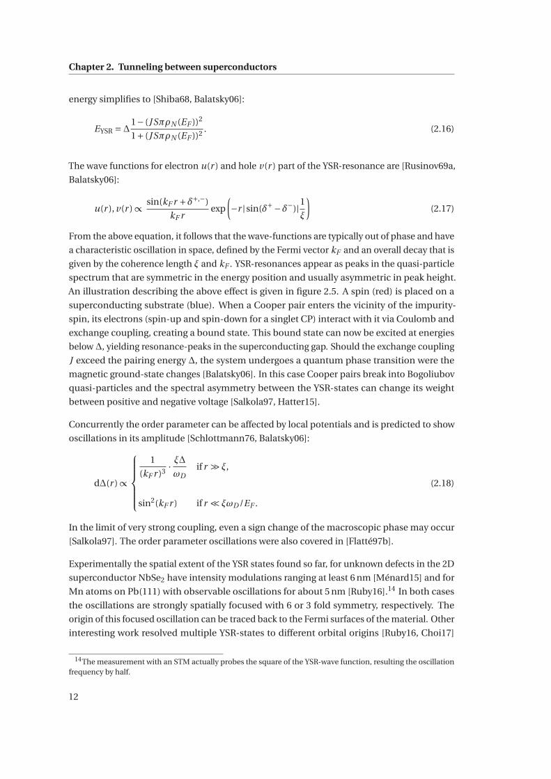
An illustration describing the above effect is given in figure 2.5. A spin (red) is placed on a
superconducting substrate (blue). When a Cooper pair enters the vicinity of the impurity-
spin, its electrons (spin-up and spin-down for a singlet CP) interact with it via Coulomb and
exchange coupling, creating a bound state. This bound state can now be excited at energies
below Δ, yielding resonance-peaks in the superconducting gap. Should the exchange coupling
J exceed the pairing energy Δ, the system undergoes a quantum phase transition were the
magnetic ground-state changes [Balatsky06]. In this case Cooper pairs break into Bogoliubov
quasi-particles and the spectral asymmetry between the YSR-states can change its weight
between positive and negative voltage [Salkola97, Hatter15].
Concurrently the order parameter can be affected by local potentials and is predicted to show
oscillations in its amplitude [Schlottmann76, Balatsky06]:
dΔ(r ) ∝
⎧⎪⎪⎪⎪⎨⎪⎪⎪⎪⎩
1
(kF r )3 · ξΔωD
if r ξ,
sin2(kF r ) if r � ξωD /EF .
(2.18)
In the limit of very strong coupling, even a sign change of the macroscopic phase may occur
[Salkola97]. The order parameter oscillations were also covered in [Flatté97b].
Experimentally the spatial extent of the YSR states found so far, for unknown defects in the 2D
superconductor NbSe2 have intensity modulations ranging at least 6 nm [Ménard15] and for
Mn atoms on Pb(111) with observable oscillations for about 5 nm [Ruby16].14 In both cases
the oscillations are strongly spatially focused with 6 or 3 fold symmetry, respectively. The
origin of this focused oscillation can be traced back to the Fermi surfaces of the material. Other
interesting work resolved multiple YSR-states to different orbital origins [Ruby16, Choi17]
14The measurement with an STM actually probes the square of the YSR-wave function, resulting the oscillationfrequency by half.
12
2.2. Superconductivity
DO
S
Energy
DO
S
Energy
DO
S
Energy
J+U
Figure 2.5 – Sketch of an impurity interaction with a superconducting host. An impurity(red) has a Coulomb potential U and an exchange potential J , which interact with a nearbyCooper pair. This interaction leads to a bound state, which gives YSR-resonance peaks in thedensity of states with typically asymmetric peak height. A local spectroscopy will measureoscillations of the peak intensity with distance r from the impurity center, until it decayed.Directly at scattering center the coherence peaks of the superconducting host are suppressed,further away a convolution of the YSR-peaks with the SC-gap is detected.
and study the effect of hybridization between single impurities [Ji08, Kezilebieke18, Choi].
Also the interplay of the YSR-effect and the Kondo-effect [Kondo64], coincidentally result-
ing from magnetic interactions with conduction electrons, was under investigation [Franke11].
YSR-states in a BCS superconductor are protected from decay channels inside the gap [Heinrich13]
but can experience some broadening induced by thermal decay [Ruby15a] or residual quasi-
particles in the gap [Martin14]. In unconventional SCs, the situation can be different, for
instance in d-wave SCs because of their non-trivial order parameter they display an intrinsic
broadening of YSR-states [Salkola97, Hudson01]. YSR-resonances gained a lot of interest due
to their relation to the possible realization of Majorana bound states in magnetic chains on a
superconducting surface [Nadj-Perge14, Ruby15a].
We will return to the topic of YSR-resonances, concerning magnetic interactions with a super-
conductor with a complex valued and energy dependent order parameter, in chapter 6. We
will show theoretical calculations and experimental data demonstrating YSR-peaks outside of
the gap and resolve the origin of their significant spectral broadening.
13
Chapter 2. Tunneling between superconductors
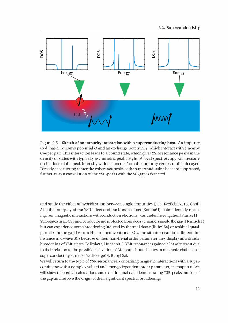
SC 1 SC 2weak link
Δ(φ2) = |Δ2|eiΦ2Δ(φ1) = |Δ1|eiΦ1
Figure 2.6 – Sketch of the wave function overlap af two superconducting baths. Similar asquasi-particles also Cooper pairs have a wave-function that extends outside of their hostmaterial. Given an overlap with another conductor Cooper pairs have a finite probabilityto travel trough the energy barrier. If the second electrode is a superconductor the transferoccurs without the need of an bias energy. The current flow is driven by the difference of thephases Φ1,2. Its amplitude is defined by the size of the involved order parameters |Δ1,2| and thenormal state conductance at Fermi energy GN(EF ). The actual maximal experimental currentis reduced by broadening effects, interactions with the environment to the so called switchingcurrent Is.
2.2.2 The Josephson effect
Brian Josephson derived the theory for the tunneling of Cooper pairs between superconductors
in 1962 [Josephson62, Josephson64, Josephson65]15. He concluded that the difference of the
macroscopic phases of two superconducting condensates φ = Φ1 −Φ2 drives a current at
zero voltage. The maximal Cooper pair current that the junction can support is the critical
Josephson current Ic. Two equations capture the basics of the Josephson effect. The first
describes the DC Josephson effect: at a set phase difference φ a current I will flow in the
junction at zero voltage, following [Tinkham04]:
I (t ) = Ic sin(φ(t )). (2.19)
The second yields the AC Josephson effect: a voltage V applied to the junction has as a
consequence that the phase difference will change with time:
dφ
dt= 2e
ħ V. (2.20)
Thereby an alternating current will flow with the energy νh = 2eV , enabling perfect conversion
of frequency to voltage.16 The basic element of a Josephson junction is the weak link between
two superconducting electrodes. It is not restricted to tunneling; a narrow constriction in the
15Josephson was awarded the Nobel price in Physics 1973: “for his theoretical predictions of the properties of asupercurrent through a tunnel barrier, in particular those phenomena which are generally known as the Josephsoneffects” [Nobel Media AB18].
16For this reason the Josephson effect is used as the voltage standard, by the International Organization forStandardization (ISO).
14
2.2. Superconductivity
dimensions of a superconductor is enough.
The strength of the coupling of the two phases is given by the Josephson coupling energy
[Tinkham04]:
EJ = ħ2e
Ic, (2.21)
In the case where the weak link is a tunneling junction with identical electrodes, the critical
current is given by the Ambegaokar-Baratoff relation [Ambegaokar63]:
Ic =GNπΔ
2etanh
(Δ
2kBT
). (2.22)
GN is the normal state conductance and T the temperature. In the limit of zero temperature it
reduces to:
Ic =GNπΔ
2e. (2.23)
The Josephson effect also crucially depends on the ratios of the Josephson coupling energy EJ
and the charging energy of the junction EC [Iansiti87]:
EC = Q2
2CJ, (2.24)
as well as the thermal energy Eth:
Eth = kBT. (2.25)
Significant thermal noise (Eth) or capacitive noise (EC) in the junction, compared to EJ, can
induce a premature switching out of the Cooper pair transport branch, because they induce
fluctuations of the phase difference φ. This results in a finite slope in the IV -curve around
zero voltage and a reduced maximal current the junction can support, defined as the switching
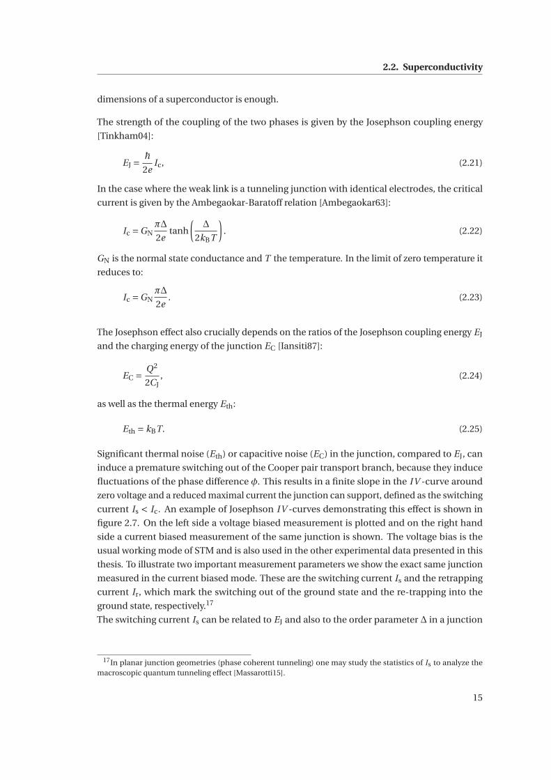
current Is < Ic. An example of Josephson IV -curves demonstrating this effect is shown in
figure 2.7. On the left side a voltage biased measurement is plotted and on the right hand
side a current biased measurement of the same junction is shown. The voltage bias is the
usual working mode of STM and is also used in the other experimental data presented in this
thesis. To illustrate two important measurement parameters we show the exact same junction
measured in the current biased mode. These are the switching current Is and the retrapping
current Ir, which mark the switching out of the ground state and the re-trapping into the
ground state, respectively.17
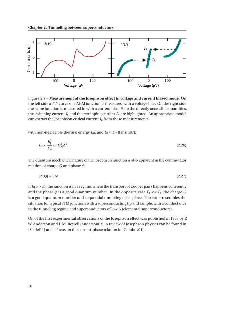
The switching current Is can be related to EJ and also to the order parameter Δ in a junction
17In planar junction geometries (phase coherent tunneling) one may study the statistics of Is to analyze themacroscopic quantum tunneling effect [Massarotti15].
15
Chapter 2. Tunneling between superconductors
I(V ) V (I)
1000-100 1000-100Voltage (μV)
IS
IR
Voltage (μV) Voltage (μV)Voltage (μV)
1
0
-1Cu
rren
t(ar
b.u
.)
Figure 2.7 – Measurement of the Josephson effect in voltage and current biased mode. Onthe left side a IV -curve of a Al-Al junction is measured with a voltage bias. On the right sidethe same junction is measured in with a current bias. Here the directly accessible quantities,the switching current Is and the retrapping current IR are highlighted. An appropriate modelcan extract the Josephson critical current Ic from these measurements.
with non-neglegible thermal energy Eth and EJ ≈ EC [Iansiti87]:
Is ∝E 2
J
EC∝G2
NΔ2. (2.26)
The quantum mechanical nature of the Josephson junction is also apparent in the commutator
relation of charge Q and phase φ:
[φ,Q] = 2ıe (2.27)
If EJ >> EC the junction is in a regime, where the transport of Cooper pairs happens coherently
and the phase φ is a good quantum number. In the opposite case EJ << EC the charge Q
is a good quantum number and sequential tunneling takes place. The latter resembles the
situation for typical STM junctions with a superconducting tip and sample, with a conductance
in the tunneling regime and superconductors of low Δ (elemental superconductors).
On of the first experimental observations of the Josephson effect was published in 1963 by P.
W. Anderson and J. M. Rowell [Anderson63]. A review of Josephson physics can be found in
[Seidel11] and a focus on the current-phase relation in [Golubov04].
16
3 Description of the experimental setup
3.1 The milli-Kelvin scanning tunneling microscope
The milli-Kelvin scanning tunneling microscope (mK-STM) was designed with the focus on
reaching the limit in energy resolution for an STM experiment. A main obstacle in realizing
this is the vibrational noise that a dilution refrigerator, which is necessary to cool down to
milli-Kelvin temperatures continuously, may introduce to the STM junction.1 Another very
important point is allowing as little electromagnetic radiation as possible to get to the junction,
because it would add an effective temperature, broadening spectroscopic features. The system
comprises an ultra-high vacuum (UHV) preparation chamber for sputtering, annealing and
cleaving of samples. Also several evaporators are mounted to expand the realm of sample
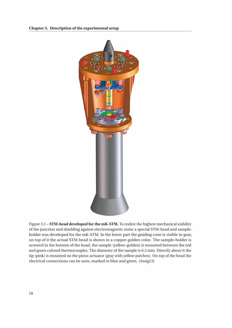
systems to explore. To ensure the highest junction stability against mechanical vibrations a
new STM-head was developed for the mK-STM, it is shown in figure 3.1. The sample transfer
is realized from the bottom of the cryostat and has no line of sight. To prevent damaging
the sample during transfer a guiding cone is mounted on the STM-head, directing the tip
and sample in the correct position. An important point in the design is that the STM-head
is completely closed, once the sample is screwed in. Having the junction fully enclosed
with a metal shielding at base temperature helps to reach the best energy resolution. The
construction and first experiments were published in 2013 and are detailed in the PhD-thesis
of Maximilian Assig [Assig11, Assig13]. He demonstrated an effective temperature of 38 mK
by fitting the superconducting gap of Al. This can also be expressed as a spectral energy
broadening of δE = 3.5kBT = 11.4μeV.
Experimental work with this new experiment covered, for instance, probing absolute spin
polarization at the atomic scale [Eltschka14], based on the Tedrow-Meservey-Fulde (TMF)
effect [Meservey94]. In this technique the spin-splitting of the superconducting density of
states under magnetic fields, and the resulting spin dependent tunneling is used to resolve the
magnetic structure of a sample. In this publication the variations of the spin-polarization of
Co nano-island on Cu(111) were studied. Additionally, it was shown that the spin-polarization
1There are several other STM setups based on dilution refrigeration, e.g. [Moussy01, Suderow02, Kambara07,Song10, Marz10, Misra13, Roychowdhury14]
17
Chapter 3. Description of the experimental setup
Figure 3.1 – STM-head developed for the mK-STM. To realize the highest mechanical stabilityof the junction and shielding against electromagnetic noise a special STM-head and sample-holder was developed for the mK-STM. In the lower part the guiding cone is visible in gray,on top of it the actual STM-head is shown in a copper-golden color. The sample-holder isscrewed in the bottom of the head, the sample (yellow-golden) is mounted between the redand green colored thermocouples. The diameter of the sample is 6.2 mm. Directly above it thetip (pink) is mounted on the piezo-actuator (gray with yellow patches). On top of the head theelectrical connections can be seen, marked in blue and green. [Assig13]
18
3.1. The milli-Kelvin scanning tunneling microscope
of the tunneling current depends on the tip-sample distance, demonstrating the different
extend of spin-states into the vacuum. Furthermore, some first experiments concerning
YSR-resonances from the interaction of CuPc-molecules on a V(100) surface were realized.
This topics are part of the PhD-thesis of Matthias Eltschka [Eltschka15].
Another field of research with the mK-STM focused on the Josephson effect in STM junctions.
It could be shown that the Cooper pair tunneling in the STM is characterized by the dynamical
Coulomb blockade regime and the critical Josephson current Ic can be extracted from IV -
curves with the P(E)-model. A result from this was the advance in the understanding of how
the tunneling process in an STM at ultra-low temperatures is influenced by its electromagnetic
environment. The electromagnetic environment was found to be given by the capacitance
between tip and sample and by the tip’s behavior as an λ/4-antenna [Jäck15b]. The findings
about this research are detailed in the PhD-thesis of Berthold Jäck [Jäck15].
The work presented in this thesis would certainly not have been possible without the important
research of the previous PhD-students.
3.1.1 Operation principle
The cooling of the mK-STM is based a dilution refrigerator inset, which is shielded by liquid
helium and nitrogen tanks from ambient temperature. The STM-head is thermally connected
to the mixing chamber of the dilution refrigerator, the coldest point in the system.
Boiling of liquid nitrogen can introduce significant vibrations to STM experiments, to eliminate
this disturbance we freeze the nitrogen, using a vacuum pump. In a dilution refrigerator
system, achieving a temperature in the range of milli-Kelvin uses the separation of a 3He rich
and a 3He poor phase of a 3He-4He mixture [Assig11]. The mixture is pre-cooled by coupling
it to a helium reservoir at 1 K. This so-called 1 K-pot is cooled by pumping it with a vacuum
pump. It can be used in a constant mode, where the flow from the helium tank is regulated with
a needle-valve to achieve an equilibrium between the evaporated helium gas and the liquid
helium refilling the reservoir. We found that this continuous mode introduces vibrations to the
system, which reduce the junction stability significantly, therefore we operate the 1 K-pot in a
single shot mode. This can easily be achieved, by closing the needle-valve which regulates the
flow to the 1 K-pot. The possible continuous operation length of the system does not decrease
because of this action, it is limited by the time the nitrogen tank empties, which is about 30 h.
In this mode we get a strongly reduced level of mechanical vibrations in the junction.
To realize an STM with a dilution refrigerator needs strong pumps to cycle the mixture, which
can introduce mechanical noise to the tunnel junction. An important task is therefore to find
ways, to move the vacuum pumps away from the actual junction and to hinder vibrations
and sound waves to travel along the necessary tube connections. Furthermore, the junction’s
susceptibility to noise should be reduced as much as possible.
An important measure to reach high spectral energy resolution, is to keep radio-frequency
(RF) radiation from getting to the STM’s juntion. This was realized by adding filters with a
cutoff frequency of about 10 kHz to all electrical connectors on the cryostat. More specifics of
the cooling and operation are described in detail in the PhD thesis of M. Assig [Assig13].
19
Chapter 3. Description of the experimental setup
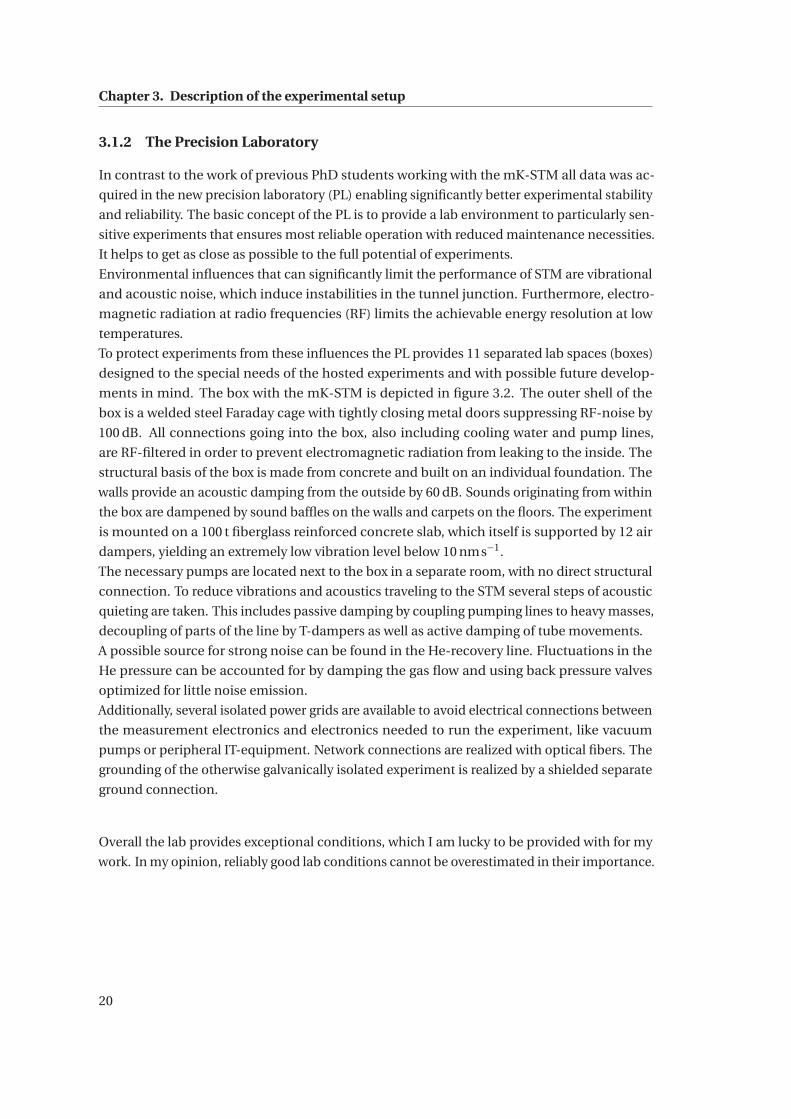
3.1.2 The Precision Laboratory
In contrast to the work of previous PhD students working with the mK-STM all data was ac-
quired in the new precision laboratory (PL) enabling significantly better experimental stability
and reliability. The basic concept of the PL is to provide a lab environment to particularly sen-
sitive experiments that ensures most reliable operation with reduced maintenance necessities.
It helps to get as close as possible to the full potential of experiments.
Environmental influences that can significantly limit the performance of STM are vibrational
and acoustic noise, which induce instabilities in the tunnel junction. Furthermore, electro-
magnetic radiation at radio frequencies (RF) limits the achievable energy resolution at low
temperatures.
To protect experiments from these influences the PL provides 11 separated lab spaces (boxes)
designed to the special needs of the hosted experiments and with possible future develop-
ments in mind. The box with the mK-STM is depicted in figure 3.2. The outer shell of the
box is a welded steel Faraday cage with tightly closing metal doors suppressing RF-noise by
100 dB. All connections going into the box, also including cooling water and pump lines,
are RF-filtered in order to prevent electromagnetic radiation from leaking to the inside. The
structural basis of the box is made from concrete and built on an individual foundation. The
walls provide an acoustic damping from the outside by 60 dB. Sounds originating from within
the box are dampened by sound baffles on the walls and carpets on the floors. The experiment
is mounted on a 100 t fiberglass reinforced concrete slab, which itself is supported by 12 air
dampers, yielding an extremely low vibration level below 10 nms−1.
The necessary pumps are located next to the box in a separate room, with no direct structural
connection. To reduce vibrations and acoustics traveling to the STM several steps of acoustic
quieting are taken. This includes passive damping by coupling pumping lines to heavy masses,
decoupling of parts of the line by T-dampers as well as active damping of tube movements.
A possible source for strong noise can be found in the He-recovery line. Fluctuations in the
He pressure can be accounted for by damping the gas flow and using back pressure valves
optimized for little noise emission.
Additionally, several isolated power grids are available to avoid electrical connections between
the measurement electronics and electronics needed to run the experiment, like vacuum
pumps or peripheral IT-equipment. Network connections are realized with optical fibers. The
grounding of the otherwise galvanically isolated experiment is realized by a shielded separate
ground connection.
Overall the lab provides exceptional conditions, which I am lucky to be provided with for my
work. In my opinion, reliably good lab conditions cannot be overestimated in their importance.
20
3.1. The milli-Kelvin scanning tunneling microscope
Filteredfeedthroughs
100 dBRF-shielding
60 dBacoustic shielding
UHV preparationchamber
Cryostat
Vibrationaldecoupling
Pump box
Figure 3.2 – The mK-STM in the Precission Laboratory Here the mK-STM is shown in itsnew lab environment located in the Precision Laboratory. Electromagnetic, acoustic andvibrational shielding/decoupling guaranty excellent working conditions for most sensitiveexperiments. The lab (box) has two floors, in the lower one the preparation chamber of theSTM can be accessed and samples/tips are transfered from here. The preparation chamber ismounted at the bottom of the cryostat without any electrically conducting connection to it.The STM-head’s position in the cryostat is approximately where the line is pointing that marksthe cryostat. The whole experiment is mounted on a 100 t concrete slab in the upper floor. Ithas no connection to the walls and is fully supported on air springs (yellow). Here, on top ofthe cryostat are all the electrical connection going to the STM. Also the tubing for cycling themixture and pumping the 1 K-pot and the nitrogen tank are going from here to the pump boxnext to the box with the experiment.
21
Chapter 3. Description of the experimental setup
0 1 2 3 4 5 6 7 8
x (nm)z noise (fm)z
(pm
) 0.5
-0.5
0
300
100
200
0
Co
un
t
-400 -200 0 200 400
b)a)
Figure 3.3 – Mechanical stability of the experimental setup. In a) the STM’s junction stabilityis analyzed in form of a histogram. It shows the noise obtained in a measurement at VT = 1V,IT = 1nA without feedback. A Gaussian fit yields a FWHM value of 250 fm. b) shows thetopography of an Al(100) crystal, VT = 10mV, IT = 1nA. In white the position of the line cutbelow (representing raw data) is highlighted. It attests the high stability level realizable in adilution refrigerator STM setup. All data taken at 15 mK.
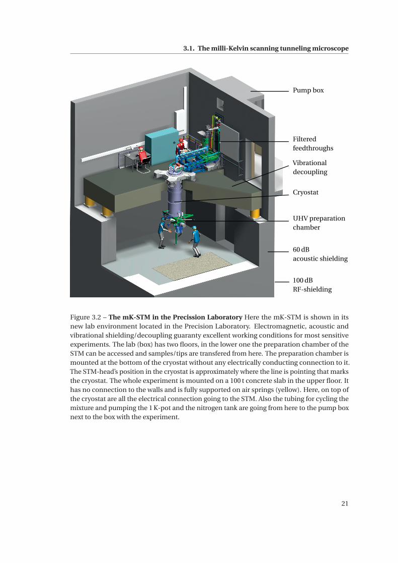
3.1.3 Stability improvements
Here we want to give an idea about the enhancement of the STM-stability achieved by moving
the machine to the PL and carefully optimizing the operation conditions. As described in
the thesis of Maximilian Assig [Assig11] the vibrational noise between tip and sample in the
old laboratory, located in the sixth floor of the institutes main building, was about 3.8 pm
(FWHM). In comparison, after installing the mK-STM in Box 1 of the PL, as shown in figure 3.2
the typical vibrational noise reduced down to 250 fm. The data and fit of this measurement is
depicted as a histogram in figure 3.3 a). This value of the mechanical stability is obtained with
a sampling period of 20 ms. In figure 3.3 b) we present topography of an Al(100) crystal with a
line scan of raw data attesting the excellent stability while operating the dilution refrigeration
cycle.
3.1.4 Energy resolution enhancement
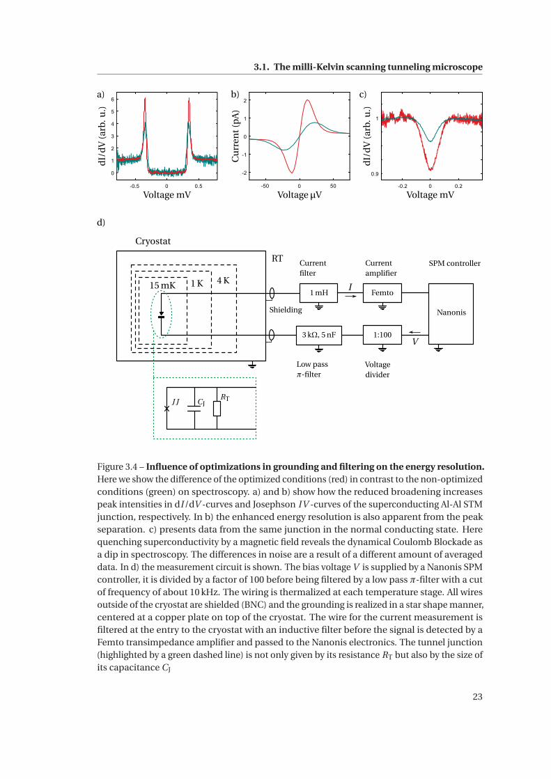
Working on the optimization of the STM we could enhance the energy resolution significantly
by changing the electric grounding concept. A comparison of data before (green) and after
(red) the change can be seen in figure 3.4. In (a) quasi-particle (QP) spectra are shown and in
(b) Josephson IV-curves (J-IV). The data was acquired with an aluminum tip and an Al(100)-
sample in the superconducting state at a temperature of 15 mK. In (c) the same junction was
driven to the normal conducting state by applying a magnetic field at the same temperature.
In this state the dynamical Coulomb blockade can be seen as a dip in spectroscopy, again
revealing the increase of resolution. Panel d) shows the measurement circuit. The wires are
low-pass filtered at the entry to the cryostat and carefully thermalized at all temperature stages.
In the following we will introduce a model to describe the energy resolution in the STM and its
dependence on the junction details.
22
3.1. The milli-Kelvin scanning tunneling microscope
dI/
dV
(arb
.u.)
dI/
dV
(arb
.u.)
Voltage μVVoltage mV Voltage mV
RT
Voltagedivider
15 mK 1 K 4 K
Low passπ-filter
Cryostat
Currentfilter
CJRT
I
V
Shielding
1 mH
1:100
Femto
3 kΩ, 5 nF
J J
Cu
rren
t(p
A)
a) b) c)
d)
SPM controllerCurrentamplifier
Nanonis
Figure 3.4 – Influence of optimizations in grounding and filtering on the energy resolution.Here we show the difference of the optimized conditions (red) in contrast to the non-optimizedconditions (green) on spectroscopy. a) and b) show how the reduced broadening increasespeak intensities in dI /dV -curves and Josephson IV -curves of the superconducting Al-Al STMjunction, respectively. In b) the enhanced energy resolution is also apparent from the peakseparation. c) presents data from the same junction in the normal conducting state. Herequenching superconductivity by a magnetic field reveals the dynamical Coulomb Blockade asa dip in spectroscopy. The differences in noise are a result of a different amount of averageddata. In d) the measurement circuit is shown. The bias voltage V is supplied by a Nanonis SPMcontroller, it is divided by a factor of 100 before being filtered by a low pass π-filter with a cutof frequency of about 10 kHz. The wiring is thermalized at each temperature stage. All wiresoutside of the cryostat are shielded (BNC) and the grounding is realized in a star shape manner,centered at a copper plate on top of the cryostat. The wire for the current measurement isfiltered at the entry to the cryostat with an inductive filter before the signal is detected by aFemto transimpedance amplifier and passed to the Nanonis electronics. The tunnel junction(highlighted by a green dashed line) is not only given by its resistance RT but also by the size ofits capacitance CJ
23
Chapter 3. Description of the experimental setup
3.2 The physical characteristics of mK-STM
Scanning tunneling microscopy and spectroscopy at ultra-low temperatures is strongly af-
fected by quantum effects inherent to the experiment. Spectroscopic measurements have to
be analyzed taking into account these effects. At a temperature of 15 mK the thermal energy
Eth is so small that characteristics of the STM junction itself like the charging energy EC and
even the electromagnetic behavior of the tip define the physics under investigation [Jäck15b].
A large charging energy in relation to a small thermal energy leads to a dynamical Coulomb
blockade (DCB), which is directly observable as a dip in the conductance around zero voltage,
with normal conducting tip and sample. We will now focus on the implications of this for the
understanding of the physical phenomena under investigation.
3.2.1 The Dynamical Coulomb Blockade
The dynamical Coulomb blockade (DCB) is a consequence of the quantization of charge, the
capacitive nature of tunnel junctions and their electromagnetic environment. This quantum
effect becomes observable, when the charging energy of the junction is large compared to the
thermal energy Eth � EC. The DCB is a dissipation effect for tunneling [Caldeira83, Devoret90].
A particle of charge Q can only tunnel, if it can excite an electromagnetic mode of the en-
vironment [Levy Yeyati01, Golubev01, Levy Yeyati05]. In a normal conducting junction this
results in a reduction of the tunneling probability around zero voltage. It can be understood
as a quantum back-action on the tunneling particles in STM, which probe the sample. In a
tunnel junction with a capacitance CJ in the range of fF the blockade can be detectable up to a
temperature of about 1 K.
The DCB is different from a Coulomb blockade, as observable for instance in a single electron
transistor, were the blockade is a result of having no state available for tunneling. This naturally
leads to a suppression of conductance, until states become available at high enough energy.
The energy exchange of the tunneling particles with the electromagnetic environment can be
accounted for by the P(E)-theory, if the junction is in the low transmission range [Devoret90].
The DCB manifests as a dip in the differential conductance at zero bias for normal conducting
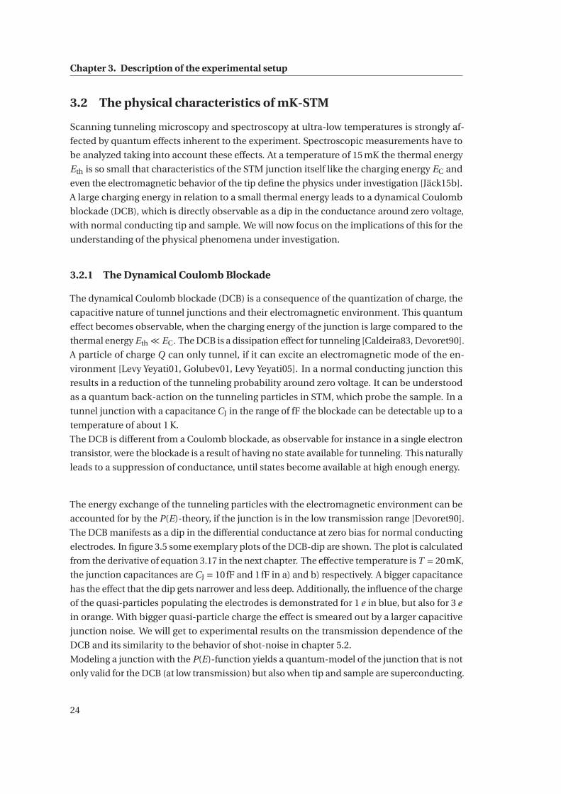
electrodes. In figure 3.5 some exemplary plots of the DCB-dip are shown. The plot is calculated
from the derivative of equation 3.17 in the next chapter. The effective temperature is T = 20mK,
the junction capacitances are CJ = 10fF and 1fF in a) and b) respectively. A bigger capacitance
has the effect that the dip gets narrower and less deep. Additionally, the influence of the charge
of the quasi-particles populating the electrodes is demonstrated for 1 e in blue, but also for 3 e
in orange. With bigger quasi-particle charge the effect is smeared out by a larger capacitive
junction noise. We will get to experimental results on the transmission dependence of the
DCB and its similarity to the behavior of shot-noise in chapter 5.2.
Modeling a junction with the P(E)-function yields a quantum-model of the junction that is not
only valid for the DCB (at low transmission) but also when tip and sample are superconducting.
24
3.2. The physical characteristics of mK-STM
-0.5 0 0.5Voltage (mV)
0.9
0.92
0.94
0.96
0.98
1D
OS
(arb
.u.)
-0.5 0 0.5Voltage (mV)
0.88
0.9
0.92
0.94
0.96
DO
S(a
rb.u
.)
C J = 1fFC J = 10fF
a) b)
1e3e
T = 20mK
Figure 3.5 – Model of the dynamical Coulomb blockade. Comparison of the DCB for differentjunction capacitances CJ = 10fF,1fF in a) and b) respectively. The temperature of the junctionis T = 20mK. Additionally, the dip is modeled not only for a quasi-particle charge Q of 1 e inblue, but also for 3 e in orange, to illustrate its influence. On top of the reduction the dipsshow a structure that relates to the details of the electromagnetic environment, i.e. possibleresonance modes.
Taking it as the basis to describe broadening in quasi-particle spectra and IV -curves of the
Josephson effect [Ingold94], the tunneling of Cooper pairs around zero voltage, achieves
excellent quantitative agreement with experimental data. We will demonstrate this in the
following.
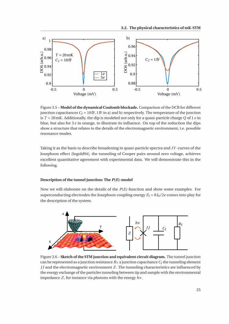
Description of the tunnel junction: The P(E)-model
Now we will elaborate on the details of the P(E)-function and show some examples. For
superconducting electrodes the Josephson coupling energy EJ =ħI0/2e comes into play for
the description of the system.
hνJ J CJ
RTy
z
x
Z
Figure 3.6 – Sketch of the STM junction and equivalent circuit diagram. The tunnel junctioncan be represented as a junction resistance RT a junction capacitance CJ the tunneling elementJ J and the electromagnetic environment Z . The tunneling characteristics are influenced bythe energy exchange of the particles tunneling between tip and sample with the environmentalimpedance Z , for instance via photons with the energy hν.
25
Chapter 3. Description of the experimental setup
eV
P(E)
E
Tip Sample
Figure 3.7 – Energy diagram for tunneling in the dynamical Coulomb blockade regime. Par-ticles tunneling in the dynamical Coulomb blockade regime interact with the surroundingelectromagnetic environment and can lose or gain energy by photon exchange with it. Elec-trons traveling through the vacuum between tip and sample will end in an energy distributiondescribed by the P(E)-model. Taken from [Ast16].
The ratio of the three characterizing energies defines the physical regime of the junction.
If EJ � EC, the DCB has a characterizing order, Cooper Pairs (CP) tunnel sequentially, and
EJ can be regarded as a perturbation of EC. A suitable analytical approach to model the
dynamical Coulomb blockade dip as well as the Josephson IV -curve is the P(E)-theory. It gives
a probability for inelastic energy exchange between the tunneling particle and the environment
[Ingold92, Ingold94]. It yields a characteristic quantum-model for a junction describing the
quantum back-action on the tunneling particles. We find that it agrees excellently with our
data for DCB-dip, Josephson IV -curve and quasi-particle (QP) spectra, where it reduces fit
parameters to RN and Δ.
In figure 3.6 the STM-juntion is represented on the left. On the right an equivalent circuit
diagram of the junction is shown. The image of the STM junction helps to highlight the
differences to other geometries, were the P(E)-model was used before. First, the weak link
between the electrodes is not a constriction or an insulating oxide layer but vacuum. Second,
the tip-electrode acts as a λ/4-antenna and has a dominating role in the electromagnetic
environment [Jäck15]. These details are shown again in the equivalent circuit diagram in
b). The Josephson junction can be represented by the Josephson contact (J J), the junction
capacitance CJ and tunneling resistance RT in parallel. Additionally, the vacuum impedance
Z , with which the inelastic energy transfer of the tunneling particles takes place, is included.
The exchange of photons with energy hν is symbolized by arrows.
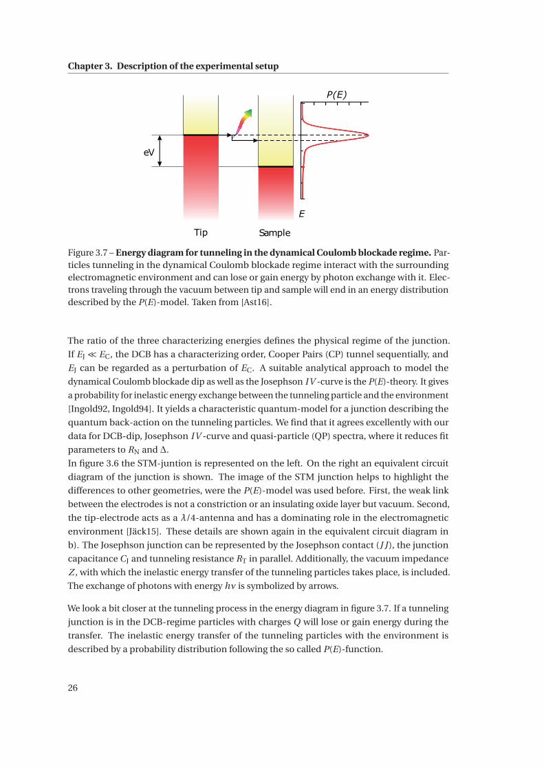
We look a bit closer at the tunneling process in the energy diagram in figure 3.7. If a tunneling
junction is in the DCB-regime particles with charges Q will lose or gain energy during the
transfer. The inelastic energy transfer of the tunneling particles with the environment is
described by a probability distribution following the so called P(E)-function.
26
3.2. The physical characteristics of mK-STM
a) b)
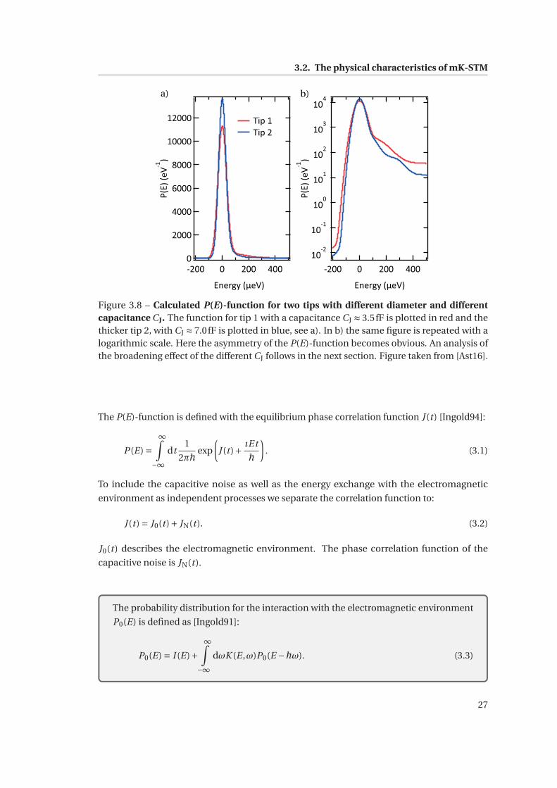
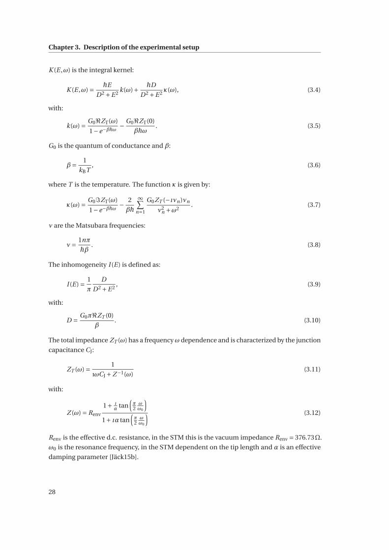
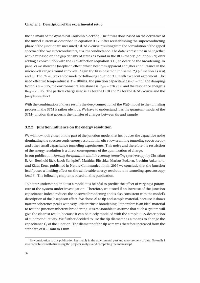
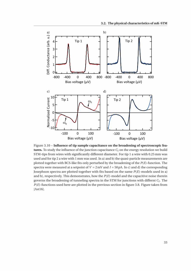
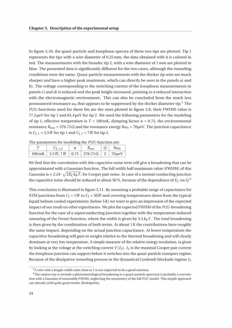
Figure 3.8 – Calculated P(E)-function for two tips with different diameter and differentcapacitance CJ. The function for tip 1 with a capacitance CJ ≈ 3.5fF is plotted in red and thethicker tip 2, with CJ ≈ 7.0fF is plotted in blue, see a). In b) the same figure is repeated with alogarithmic scale. Here the asymmetry of the P(E)-function becomes obvious. An analysis ofthe broadening effect of the different CJ follows in the next section. Figure taken from [Ast16].
The P(E)-function is defined with the equilibrium phase correlation function J (t ) [Ingold94]:
P (E) =∞∫
−∞dt
1
2πħ exp
(J (t )+ ıEt
ħ)
. (3.1)
To include the capacitive noise as well as the energy exchange with the electromagnetic
environment as independent processes we separate the correlation function to:
J (t ) = J0(t )+ JN(t ). (3.2)
J0(t) describes the electromagnetic environment. The phase correlation function of the
capacitive noise is JN(t ).
The probability distribution for the interaction with the electromagnetic environment
P0(E) is defined as [Ingold91]:
P0(E) = I (E)+∞∫
−∞dωK (E ,ω)P0(E −ħω). (3.3)
27
Chapter 3. Description of the experimental setup
K (E ,ω) is the integral kernel:
K (E ,ω) = ħE
D2 +E 2 k(ω)+ ħD
D2 +E 2 κ(ω), (3.4)
with:
k(ω) = G0ℜZT(ω)
1−e−βħω− G0ℜZT(0)
βħω . (3.5)
G0 is the quantum of conductance and β:
β= 1
kBT, (3.6)
where T is the temperature. The function κ is given by:
κ(ω) = G0ℑZT(ω)
1−e−βħω− 2
βħ∞∑
n=1
G0ZT (−ıνn)νn
ν2n +ω2
. (3.7)
ν are the Matsubara frequencies:
ν= 1nπ
ħβ . (3.8)
The inhomogeneity I (E) is defined as:
I (E) = 1
π
D
D2 +E 2 , (3.9)
with:
D = G0πℜZT (0)
β. (3.10)
The total impedance ZT (ω) has a frequency ω dependence and is characterized by the junction
capacitance CJ:
ZT (ω) = 1
ıωCJ +Z−1(ω)(3.11)
with:
Z (ω) = Renv
1+ ıα tan
(π2
ωω0
)1+ ıα tan
(π2
ωω0
) (3.12)
Renv is the effective d.c. resistance, in the STM this is the vacuum impedance Renv = 376.73Ω.
ω0 is the resonance frequency, in the STM dependent on the tip length and α is an effective
damping parameter [Jäck15b].
28
3.2. The physical characteristics of mK-STM
The probability distribution describing the thermal capacitive noise PN(E) is modeled
by a Gaussian [Ingold94]:
PN(E) = 1√4πECkBT
exp
(− E 2
4πECkBT
). (3.13)
The capacitive energy of the junction depends on the charge Q of the particles that populate it.
It follows the relation:
EC = Q2
2CJ. (3.14)
The full P(E)-function including the environmental part P0(E ) and the capacitive noise
PN (E) is then given by their convolution:
P (E) =∞∫
−∞dE ′P0(E −E ′)PN (E ′). (3.15)
The shape of the P(E)-function is displayed in figure 3.8. We have used two different junction
capacitances (tip 1 and tip 2) the capacitance values are CJ(tip 1) ≈ 3.5fF and CJ(tip 2) ≈ 7.0fF.
In a) the curves are plotted on a linear scale, revealing a reduced peak height for tip 1 with
a smaller capacitance. The difference in the width of the two curves can be seen in the
semi-logarithmic plot in b). The peak corresponding to tip 1 is broader. Because the P(E)-
function obeys the detailed balance symmetry [Ingold91] the overall shape of the function is
asymmetric. This asymmetry stems from the P0(E)-function and the main part of the width
from the capacitive noise in the junction, which are convolved. We will detail on this junction
inherent broadening effect in the next section.
29
Chapter 3. Description of the experimental setup
Deriving the tunneling probability in the junction under this inelastic influence, one
obtains for one direction [Odintsov88, Devoret90]:
−→Γ (V ) = GT
e2
∞∫−∞
∞∫−∞
dEdE ′ρs(E ′ +eV )ρt (E) f (E)[1− f (E ′ +eV )]P (E −E ′) (3.16)
with the Fermi function f (E ) = 1/(1+exp(E/kBT )). In the case of vanishing interaction
with the environment the P(E)-function is simply given by the delta function P (E) =δ(E) and the standard symmetric transfer for tunneling is retained. The tunneling
current is given by the difference of the tunneling rates in both directions:
I (V ) = e(−→Γ (V )−←−
Γ (V ))
. (3.17)
The parameters for modeling the P(E)-function are:Effective Junction Damping Environmental Particle Resonance
temperature capacitance factor resistance charge frequency
Teff CJ α Renv Q ω0
Let us now consider the Josephson effect in this in the DCB regime, with a Josephson cou-
pling energy EJ much smaller than the capacitive charging energy EC. For some previous
STM experiments the Ivanchenko-Zil’berman model [Ivanchenko69] was used to explain the
data. Because this model is only valid in the classical phase diffusion limit, were EC << Eth
[Ivanchenko69, Ingold94], we cannot use it, because we are certainly not operating our exper-
iment in this regime but rather in the opposite range, with EC >> Eth. Additionally, the reso-
nances of the antenna like behavior of the STM-tip are not accounted for in the Ivanchenko-
Zil’berman model. STM experiments with low Tc superconductors should generally be in the
range, where the capacitive energy is larger than the Josephson coupling energy and therefore
in the tunneling regime that is characterized by sequential transfer of charges.
For the description of the Josephson current the Josephson coupling energy EJ basically
acts as a scaling parameter [Ingold94]:
I (V ) =πeE 2
J
ħ [P (2eV )−P (−2eV )] (3.18)
To develop a comprehensive picture of the sequential charge tunneling in the DCB let us now
consider its effect on some experimental examples. In figure 3.9 the P(E)-model is used to
describe measurements of three different physical phenomena. Note that the same P(E)-
function was used in all three fits. In a) the junction was forced to its normal conducting state
with a magnetic field of 10 mT to measure the conductance dip around zero voltage, which is
30
3.2. The physical characteristics of mK-STM
a)
b) c)
Figure 3.9 – Modelling the Josephson effect, quasi-particle tunneling and the dynamicalCoulomb blockade based on one characteristic P(E)-function. Here we demonstrate, howthe junction characteristic P(E)-model is able to describe measurements of three differentphysical phenomena. In a) a measurement of the dynamical Coulomb blockade is modeledwith the derivative of equation 3.17. The normal conducting state of the junction was achievedby quenching superconductivity with a magnetic field of 10 mT. After turning off the magneticfield and retaining the superconducting phase in tip and sample a dI /dV -curve was mea-sured. It is shown in b). Here the same P(E)-function (equation 3.15) is used to describe thebroadening of the measurement which shows the convolution of two . The third application isthe Josephson effect. The data and the fit based on equation 3.18 is plotted in c). Also hereexcellent agreement is found between fit and measurement. Data is plotted in blue and fits inblack. Figure taken from [Ast16].
31
Chapter 3. Description of the experimental setup
the hallmark of the dynamical Coulomb blockade. The fit was done based on the derivative of
the tunnel current as described in equation 3.17. After reestablishing the superconducting
phase of the junction we measured a dI /dV -curve resulting from the convolution of the gaped
spectra of the two superconductors, at a low conductance. The data is presented in b), together
with a fit based on the gap density of states as found in the BCS-theory (equation 2.9) only
adding a convolution with the P(E)-function (equation 3.15) to describe the broadening. In
panel c) we show the Josephson effect, which becomes apparent at higher conductance in the
micro-volt range around zero volt. Again the fit is based on the same P(E)-function as is a)
and b). The IV -curve can be modeled following equation 3.18 with excellent agreement. The
used effective temperature is T = 100mK, the junction capacitance is CJ = 7fF, the damping
factor is α= 0.75, the environmental resistance is Renv = 376.73Ω and the resonance energy is
ħω0 = 70μeV. The particle charge used is 1 e for the DCB and 2 e for the dI /dV -curve and the
Josephson effect.
With the combination of these results the deep connection of the P(E)-model to the tunneling
process in the STM is rather obvious. We have to understand it as the quantum-model of the
STM-junction that governs the transfer of charges between tip and sample.
3.2.2 Junction influence on the energy resolution
We will now look closer on the part of the junction model that introduces the capacitive noise
dominating the spectroscopic energy resolution in ultra-low scanning tunneling spectroscopy
and other small capacitance tunneling experiments. This noise and therefore the restriction
of the energy resolution is a direct consequence of the quantization of charge.
In our publication Sensing the quantum limit in scannig tunneling spectroscopy, by Christian
R. Ast, Berthold Jäck, Jacob Senkpiel2, Matthias Eltschka, Markus Etzkorn, Joachim Ankerhold,
and Klaus Kern, published in Nature Communication in 2016 we conclude that the junction
itself poses a limiting effect on the achievable energy resolution in tunneling spectroscopy
[Ast16]. The following chapter is based on this publication.
To better understand and test a model it is helpful to predict the effect of varying a param-
eter of the system under investigation. Therefore, we tested if an increase of the junction
capacitance indeed reduces the observed broadening and is also consistent with the model’s
description of the Josephson effect. We chose Al as tip and sample material, because it shows
narrow coherence peaks with very little intrinsic broadening. It therefore is an ideal material
to test the junction inherent broadening. It is reasonable to assume that such a system will
give the clearest result, because it can be nicely modeled with the simple BCS-description
of superconductivity. We further decided to use the tip diameter as a means to change the
capacitance CJ of the junction. The diameter of the tip wire was therefore increased from the
standard of 0.25 mm to 1 mm.
2My contribution to this publication lies mainly in the experimental part and measurement of data. Naturally Ialso contributed with discussing the projects analysis and completing the manuscript.
32
3.2. The physical characteristics of mK-STM
a) b)
c) d)
Figure 3.10 – Influence of tip sample capacitance on the broadening of spectroscopic fea-tures. To study the influence of the junction capacitance CJ on the energy resolution we buildSTM-tips from wires with significantly different diameter. For tip 1 a wire with 0.25 mm wasused and for tip 2 a wire with 1 mm was used. In a) and b) the quasi-particle measurements areplotted together with BCS-like fits only perturbed by the broadening of the P(E)-function. Thespectra were measured at a setpoint of V = 2mV and I = 50pA. In c) and d) the correspondingJosephson spectra are plotted together with fits based on the same P(E)-models used in a)and b), respectively. This demonstrates, how the P(E)-model and the capacitive noise thereingoverns the broadening of tunneling spectra in the STM for junctions with differnt CJ. TheP(E)-functions used here are plotted in the previous section in figure 3.8. Figure taken from[Ast16].
33
Chapter 3. Description of the experimental setup
In figure 3.10, the quasi-particle and Josephson spectra of these two tips are plotted. Tip 1
represents the tips with a wire diameter of 0.25 mm, the data obtained with it is colored in
red. The measurements with the broader tip 2, with a wire diameter of 1 mm are plotted in
blue. The presented data is significantly different for the two cases, although the tunneling
conditions were the same. Quasi-particle measurements with the thicker tip wire are much
sharper and have a higher peak maximum, which can directly be seen in the panels a) and
b). The voltage corresponding to the switching current of the Josephson measurements in
panels c) and d) is reduced and the peak height increased, pointing to a reduced interaction
with the electromagnetic environment. This can also be concluded from the much less
pronounced resonance ω0 that appears to be suppressed by the thicker diameter tip.3 The
P(E)-functions used for these fits are the ones plotted in figure 3.8, their FWHM-value is
77.2μeV for tip 1 and 65.4μeV for tip 2. We used the following parameters for the modeling
of tip 1; effective temperature is T = 100mK, damping factor α = 0.75, the environmental
resistance Renv = 376.73Ω and the resonance energy ħω0 = 70μeV. The junction capacitance
is CJ, 1 = 3.5fF for tip 1 and CJ, 1 = 7fF for tip 2.
The parameters for modeling the P(E)-function are:T CJ, 1,2 α Renv Q ħω0
100 mK 3.5 fF, 7 fF 0.75 376.73Ω 2 70μeV
We find that the convolution with this capacitive noise term will give a broadening that can be
approximated with a Gaussian function. The full width half maximum value (FWHM) of this
Gaussian is ≈ 2.24 ·√2ECkBT , for Cooper pair noise. In case of a normal conducting junction
the capacitive noise should be reduced to about 50 %, because of the dependence of EC on Q.4
This conclusion is illustrated in figure 3.11. By assuming a probable range of capacitance for
STM junctions from CJ = 1fF to CJ = 50fF and covering temperatures down from the typical
liquid helium cooled experiments (below 5 K) we want to give an impression of the expected
impact of our result on other experiments. We plot the expected FWHM of the P(E)-broadening
function for the case of a superconducting junction together with the temperature induced
smearing of the Fermi-function, where the width is given by 3.5kBT . The total broadening
is then given by the combination of both terms. At about 1 K the contributions have roughly
the same impact, depending on the actual junction capacitance. At lower temperature the
capacitive broadening will gain in weight relative to the thermal broadening and will clearly
dominate at very low temperature. A simple measure of the relative energy resolution, is given
by looking at the voltage at the switching current V (IS). IS is the maximal Cooper pair current
the Josephson junction can support before it switches into the quasi-particle transport regime.
Because of the dissipative tunneling process in the dynamical Coulomb blockade regime IS
3A wire with a length-width ratio close to 1 is not expected to be a good antenna.4The easiest way to include a phenomenological broadening to a quasi-particle spectrum is probably a convolu-
tion with a Gaussian of reasonable FWHM, neglecting the asymmetry of the full P(E)-model. This simple approachcan already yield quite good results [Rodrigo04a]
34
3.2. The physical characteristics of mK-STM
Figure 3.11 – Comparison of broadening intrinsic to a junction’s capacitance with broad-ening due to temperature. To illustrate the impact of the broadening resulting from theinteraction of tunneling particles with the environment we plot the expected FWHM value ofthe P(E)-function together with broadening due to temperature. For the thermal smearing ofthe Fermi function we take the standard value 3.5kBT . To get the junction inherent part weassume a range of capacitance reasonable for the STM. Figure taken from [Ast16].
is reduced, compared to the theoretical maximum. This induces that the switching does not
happen at zero voltage, but at a finite voltage V (IS), indicating the amount of back-action on
the tunneling particles. After the optimizations during my PhD-work we find this voltage to be
about V (IS) = 11μV compared to about V (IS) = 19μV before.
3.2.3 The capacitance of the tunnel junction
Determining the actual junction capacitance and even more so the environmental impedance
of the STM junction independently is interestingly a non-trivial endeavor on its own. Simple
lock-in measurements do not only contain the immediate area of the junction, but also include
the capacitance of the wiring as well as tip and sample holder that are not of importance for
the tunneling process. Not to mention that the frequency range of the Cooper pair photon
emission lies in the GHz range, which is impossible to feed or detect in the current setup of
the STM. One approach to get an approximate answer to the magnitude of CJ is using a simple
but analytical model for the tip capacitance. We used the following equation to do so [Ast16]:
CJ = πε0d
sin(α/2) ln(cot(α/4)), (3.19)
35
Chapter 3. Description of the experimental setup
d
20 40 60 80 100 120 140 160Opening Angle (°)
50
100
150
200
250
300
Cap
acit
ance
(fF
)
250μm1 mm2 mm
αTip
Sample
Figure 3.12 – Simple analytical model to estimate the junction capacitance. Simple modelof tip and sample for estimating the junction capacitance. a) the tip is assumed to be conicaland touches the (flat) sample in one point. The diameter d of the tip wire as well as theopening angle α are indicated. Figure taken from [Ast16]. b) Relation of CJ to opening angle α
and tip diameter. Although the model is very simplistic and therefore disregards many detailsof the real junction the size of CJ lies within a factor of 10 of the values extracted from theP(E)-model.
here ε0 is the vacuum permittivity, d is the wire diameter and α is the opening angle of the tip
apex. The apex of the tip is placed directly on the sample.
The model and its parameters are visualized on the left side of figure 3.12. How the capacitance
depends on the opening angle is plotted on the right side for wire diameters of 0.25 mm in red,
1 mm in yellow and 2 mm in purple. Interestingly the model yields a minimum for α≈ 70°,
the reason for this may be an overestimation of contributions far away from the sample, with
a small opening angle the model integrates over a unrealistically long distance until the full
diameter is retained. Approaching α = 0° will give an infinite length. On the other hand a
rising CJ for large α seems very plausible. An unrealistic aspect of the model that induces
an unlikely capacitance at large opening angles is that there is no distance between tip and
sample. Both cases would anyway be extreme cases for a real tip, having an opening angle
between 40 ° and 120 ° seems plausible. The model suggests that CJ can mainly be influenced
by the wire diameter and less so by the opening angle, disregarding extremely flat tips. In
comparison to the values we used in our analysis we may underestimate the capacitance,
but regarding the simplicity of the model the results still confirm the qualitative order. A
quantitatively more meaningful model will have to be much more elaborate.
3.3 Conclusions
Operating an STM at low and ultra-low temperatures the tunneling process becomes signifi-
cantly influenced by the quantum back-action of the electromagnetic environment. In this
36
3.3. Conclusions
regime the granularity in the tunneling and the quantization of charge become non-negligible
and have to be regarded in the understanding of acquired data. The most direct observation
of this back-action is the dynamical Coulomb blockade in the normal conducting junction. It
induces a reduction of the tunneling probability around zero voltage and accordingly yields
a dip in the differential conductance. The back-action becomes observable at low tempera-
tures, where the thermal energy Eth is smaller than the capacitive energy EC of the tip sample
junction. Its behavior can be modeled in the framework of the P(E)-theory. For spectroscopic
measurements it yields a broadening function that has to be convoluted with a theoretical
model to properly reproduce the data. It can be understood as the function describing the
energy resolution in scanning tunneling spectroscopy. For the dynamical Coulomb blockade
it directly gives the characteristic dip around zero voltage. And in addition, it also models
the Josephson effect of a superconducting junction. The parameters of the P(E)-function are
the same in all cases, except for the charge because it depends on the kind of quasi-particle
populating the tip and sample. This result highlights the universality of this model for the
tunneling process in milli-Kelvin STM.
We detail on a simple possibility to reduce the quantum back-action in the junction. The
tip-sample capacitance EC and the tips behavior as an antenna appear are the main source for
the interaction of tunneling particles with the environment. Using a tip of a larger macroscopic
diameter results in a larger EC (by increasing the cross section of tip and sample) and also
makes the tip a bad antenna, which significantly increases the spectroscopic energy resolu-
tion. We conclude that up to a temperature of about 1 K the influence of the environmental
back-action can play an important role. At this temperature the thermally induced broadening
3.5kBT is of the size of the broadening expected from the P(E)-model.
Further analysis of the physical characteristics of mK-STM: A stronger focus on the physi-
cal regime and its peculiarities is beyond the scope of this thesis. For the interested reader
we want to point out our publication; Quantum Brownian Motion at Strong Dissipation
Probed by Superconducting Tunnel Junctions, authored by; Berthold Jäck, Jacob Senkpiel,
Markus Etzkorn, Joachim Ankerhold, Christian R. Ast and Klaus Kern, published in Physical
Review Letters, 2017. [Jäck17] Here we analyze current biased measurements with a quantum-
Smoluchowski equation. We demonstrate that the Josephson junction is an over damped
quantum system that behaves as expected from quasi-classical dynamics but with significant
corrections because of quantum effects.
Additionally, our following publication may be of interest; Signatures of phase-coherent trans-
port and the role of quantum fluctuations in the dynamical Coulomb blockade regime, with the
authors; Berthold Jäck, Jacob Senkpiel, Markus Etzkorn, Joachim Ankerhold, Christian R. Ast
and Klaus Kern, arXiv:1712.07172 [cond-mat.mes-hall] [Jäck18]. In this work we study the in-
terplay of internal quantum fluctuations and quantum fluctuations with external origin, both
related to different Cooper pair transport mechanisms. We find signatures of coherent Cooper
pair transport at low voltages and at higher voltages signatures for incoherent transport.
37
4 Transmission channels in atomiccontacts
In this chapter we will study the electronic transport properties of the STM junction concerning
the channels that participate and how measurements may be influenced by the channel
configuration.1 In break-junction experiments it was found that the number of transmission
channels can be traced back to the valence orbitals, by comparing experimental data with
computed Andreev reflection spectra [Scheer00]2. Orbitals giving a significant contribution
to the DOS around EF, have to be considered for as possible tunneling channels. This means
that depending on the chemical group of the metal at hand only s- and p- or additionally
also d-orbitals need to be taken into account with possible constraints due to the junction
symmetry [Cuevas98a]. Strong indications were found that the channel configuration is the
same in the superconducting and the normal conducting state of a junction [Scheer00].
The junction of choice for the experiments we conducted consists of an Al-tip and a Al(100)-
sample with one single atom at both ends. First we will analyze Andreev reflection spectra
of the junction to determine the number of participating channels and their transmission,
as has been done before. We will demonstrate that the number of significant channels can
be reduced from three (corresponding to the valence of Al) to one by STM manipulation of a
single Al-atom on the sample surface.
After that the transmission dependence of two physical phenomena, the Josephson effect and
the dynamical Coulomb blockade of the single channel junction will be studied. Concerning
the Josephson effect we will introduce a model that is non-linear in transmission and includes
multiple Cooper pair tunneling. It is based on the full Andreev bound state relation and
corresponds very well to the experimental data. At the end of this part of the thesis we will
present some early results on how the dynamical Coulomb blockade dip gets smaller with
rising transmission in a single channel system.
1Apart from the electronic transport properties also thermal conduction in atomic contacts is in the focus ofrecent publications. For instance work on the quantization of thermal transport in single atomic contacts waspublished in 2017 [Cui17].
2Experimental determination of conduction channels in atomic-scale conductors is also possible based on shotnoise measurements [Vardimon13].
39
Chapter 4. Transmission channels in atomic contacts
eV2
I
V2
e
I
V
eV2 eh
Single quasiparticle process
Andreev Reflection
eV
I
V
2
2 /3
eV2
I
V2 n
MAR
Multiple Andreev Reflection (MAR)(a) (c)
(b) (d)
Figure 4.1 – Illustration of quasiparticle tunneling and (multiple) Andreev reflections in anSIS junction. On the left side the reflection scheme is depicted and the right side the resultingcontributions to the IV-curve is shown. The Bias voltage necessary to enable the tunnelingprocess is marked as eV. The order of the tunneling process rises from panel a) to panel d).Images taken from [Cuevas99].
4.1 Andreev reflections
Let us start with a short description of what Andreev reflections are. An Andreev reflection is
one possibility of tunneling between two SC’s or an SC and a normal conductor at bias voltages
lower than Δ/e. As depicted in figure 4.1 tunneling of quasi particles in a tunnel junction of
two SC is possible, when the applied bias voltage provides enough energy to split Cooper pairs
in both electrodes, in a symmetric junction V = 2Δ/e. In an asymmetric junction made of a
superconductor and a normal conductor tunneling can occur already at V =Δ/e, only one
energy gap has to be overcome. In this case, where one electron charge e is transported from
one electrode to the other, also known as quasi-particle tunneling no transport is allowed for
energies below the superconducting gap, see figure 4.1 a). An Andreev reflection makes just
this possible. In the first order process an electron transverses the barrier but has only half the
energy needed to reach the quasi-particle continuum. It can anyway enter the superconductor,
if it forms a Cooper pair with another electron at the Fermi level and a hole is reflected, which
then enters the quasi-particle continuum of the first electrode, compare figure 4.1 b). Also
higher order processes, where multiples n of e are transferred and the reflection goes back
and forth several times is possible. These multiple Andreev reflection (MAR) are depicted in c)
and d). The energies, at which above phenomenon can happen result in steps in the current-
voltages curves at V ∼ 2Δ/ne. At n = 1 tunneling of quasi-particles occurs and dominates the
current for V ≥ 2Δe, proportional to the transmission τ. Equivalently for n = 2,3,4, ... Andreev
reflections of rising orders generate steps at V ∼ 2Δ/ne and add current above this voltage
proportional to τn , compare 4.1. The reflection process consists of transporting an electron
(hole) from electrode one to the electrode two and transporting a hole (electron) back to the
40
4.2. Modeling transport channels in atomic contacts
a) b) c)
Figure 4.2 – Experimental observation of Andreev reflections at different junction conduc-tances. In a) and b) we show normalized IV - curves and normalized dI /dV -spectra. Thefilling of the superconducting gap and the steps/peaks at the voltages corresponding to theorder of the Andreev process are visible. In c) the dependence of the maxima of coherencepeaks (QP), first (MAR1) and second (MAR2) Andreev reflection and Josephson peak (ZBP) onthe conductance is plotted. The ZBP nicely follows a quadratic dependence off G , as well asMAR1 showing deviations above currents of 20 nA. The second Andreev reflection follows G3.
first one. This effectively generates a Cooper pair in the second electrode. In case of n being
odd an additional quasi-particle is transferred to the second electrode. This series of transmis-
sion dependent reflections is the origin of the structured filling of the superconducting gap
and also an additional current outside of the gap, the excess current.
Experimental observation of Andreev processes were already published in 1963 [Taylor63].
More detailed studies followed later [Blonder82, Octavio83] and also the STM was used to
detect Andreev reflections ([Scheer98]) of asymmetric superconducting junctions, with super-
conducting gaps of different size [Ternes06]. Furthermore, they have been used to observe
local variations in the tunneling channels at the point contact limit in STM [Kim15]. We want
to show now some of our data to illustrate the filling of the gap by Andreev processes. In figure
4.2 some experimental Andreev reflection spectra are shown. In a) normalized IV -curves for
rising setpoint currents (100 pA to 50 nA), which corresponds to an equally rising conductance
are shown. The same data is plotted in b) as differential conductance. In both the data was
normalized to 1 at the setpoint conditions to make the gap filling easily observable. A simple
analysis of the peak heights in the dI /dV -data is given in c). The first order Andreev peak
(MAR1) grows quadratically with the conductance, as does the Josephson effect. The second
one (MAR2) grows with the conductance to the power of 3, as expected from theory. The strong
setpoint dependence of Andreev reflections is the key to analyzing the transport channels of a
tunnel junction.
4.2 Modeling transport channels in atomic contacts
Here one well-established theoretical framework on how to model the Andreev processes shall
be described in a manner that introduces some of the main points, but leaves out most of the
41
Chapter 4. Transmission channels in atomic contacts
details. The following will be a very condensed reproduction of the work of Juan Carlos Cuevas
et al. [Cuevas96, Cuevas98a, Cuevas98b, Cuevas99].3
To describe the analysis of our data we follow the PhD work of Juan Carlos Cuevas enabling
the extraction of number and conduction ratios of channels in an atomic junction yielding the
transmission coefficients of each channel of the contact [Cuevas99]. To model the electrical
transport in an atomic size junction the current can be split into several independent conduc-
tion channels. These channels, with their individual conductance Gi = τi ·G0 add up to the
total conductance of the junction, G0 being the quantum of conductance G0 = 2e2/h and τi
the individual transmission coefficients ranging between 0 and 1. The junction can hereby be
characterized by the full set of transmission coefficients {τi }, yielding the so called PIN-code.
Based on these the total current through N channels is given by:
I (V ) =N∑
i=1Ii (V ,τi ). (4.1)
The theoretical background to arrive at this conclusion will be described in the following,
reproducing the work of J. C. Cuevas [Cuevas99]. The single channel Hamiltonian of a quantum
point contact or tunnel junction is given by:
H = HL + HR +∑σ
(χc†LσcRσ+χ∗c†
RσcLσ)−μL NL −μR NR . (4.2)
With χ being the hopping parameter, and HL,R the BCS-Hamiltonians representing the uncou-
pled electrodes. The particle number operators are NL,R , μL,R and the electrostatic potentials
are μL,R and cLσ,Rσ and c†Lσ,Rσ
are the creation and annihilation operators, respectively. The
bias voltage is then V =μL −μR . A gauge transformation yields the time-dependent form:
H(t ) = HL + HR +∑σ
(χeıφ(t )/2c†LσcRσ+χ∗eıφ(t )/2c†
RσcLσ). (4.3)
Here t is the time and φ(t ) is the phase difference of the superconducting condensates.
Continuing from here, three different junction types can be described. First some results for
the normal conductor-insulator-normal conductor (N-I-N) case and the normal conductor-
insulator-superconductor (N-I-S) case will be presented. The reason for this is that these are
analytically solvable and basic aspects of the general description can be nicely highlighted here.
After that an equation describing the current in the S-I-S junction will be presented, without
going into any details, those can easily be looked up in the above mentioned publications and
go well beyond the scope of this thesis.
N-I-N junction: This case can be solved based on the time-independent Hamiltonian 4.2.
With a Green’s function formalism the tunneling current can be found.
3Other ways to model single channel tunneling, which may be equally suitable, e.g. [Averin95], will not beregarded here.
42
4.2. Modeling transport channels in atomic contacts
The current in the normal conducting junction is:
IN N = 2e
h
∞∫−∞
T (ω,V )[nF (ω,eV )−nF (ω)]dω. (4.4)
With energy ω and the transmission coefficient:
T (ω,V ) = 4χ2ρLL(ω−eV )ρRR (ω)
|1−χ2gLL(ω−eV ), gRR (ω)|2 . (4.5)
The electrode properties are included via the Green’s functions gLL and gRR . In the tunneling
limit, where only the first order coupling is regarded this reduces to:
T (ω,V ) ∼ 4π2χ2ρLL(ω−eV )ρRR (ω). (4.6)
This expression then gives a tunneling current identical to the description in equation 2.2.
Working in the low voltage regime with an ohmic IV -characteristic, T becomes a constant,
defining the transmission τ
T (ω,V ) � 4χ2π2ρ2(EF)
(1+χ2π2ρ2(EF))2 ≡ τ. (4.7)
ρ2(EF) is the density of states at the Fermi level. The transmission can lie between 0 and 1.
N-I-S junction Similar to the N-I-N junction also the N-I-S junction can be solved with the
time-independent approach.
The current with one superconducting electrode is:
IN S = 2e
h
∞∫0
{TN (ω)[nF (ω−eV )−nF (ω)]
+2R(ω)[nF (ω−eV )−nF (ω+eV )]}dω.
(4.8)
With the electron transmission probability:
TN (ω) =
⎧⎪⎪⎪⎪⎨⎪⎪⎪⎪⎩
0 if |ω| ≤Δ
2τα(1−Δ2/ω2)+ (2−τ)
�1−Δ2/ω2
[τ+ (2−τ)�
1−Δ2/ω2]2if |ω| ≥Δ
(4.9)
43
Chapter 4. Transmission channels in atomic contacts
ΔR
μR
χ
L R
ΔL
μL
Figure 4.3 – Schematic drawing of the single channel junction in the theoretical model.Images taken from [Cuevas99].
and the Andreev reflection probability:
R(ω) =
⎧⎪⎪⎪⎪⎪⎨⎪⎪⎪⎪⎪⎩
τ2
(2−α)2 −4(1−τ)(ω/Δ)2 if |ω| ≤Δ,
τ2(Δ/ω)2
[τ+ (2−α)�
1−Δ2/ω2]2. if |ω| ≥Δ
(4.10)
Here τ is the normal transmission coefficient. Several important points can be seen in these
equations. Tunneling of quasi-particles is only allowed outside of the gap and on the other
hand there is an additional tunneling outside of the gap resulting from reflection processes
leading to the excess current. For the conductance GN S(V ) = (2e2/h)[TN (V )+2R(V )] follows:
GN S(V ) = 4e2
h
⎧⎪⎪⎪⎪⎪⎨⎪⎪⎪⎪⎪⎩
τ2
(2−τ)2 −4(1−τ)((eV )/Δ)2 , if eV ≤Δ
α
τ+ (2−τ)√
1− (Δ/(eV ))2, if eV ≥Δ
(4.11)
which is equivalent to the result found from the scattering approach in the BTK model
[Blonder82]. The Andreev processes lead to a transport of Bogolyubov quasi-particles outside
of the gap, the excess current:
Iexc = eΔ
h
τ2
1−τ
[1− τ2
2(2−τ)�
1−τln
(1+�
1−τ
1−�1−τ
)](4.12)
which in the ballistic limit of τ= 1 becomes Iexc = 8/3 · (eΔ)/h.
S-I-S junction Solving the presented model for two superconducting electrodes is based on
the time-depended Hamiltonian 4.3. For this case only a numerical solution can be derived
44
4.2. Modeling transport channels in atomic contacts
for arbitrary transmissions. In contrast, for the limits of transmission τ= 0 or τ= 1 also an
analytical solution can be found. The model is developed for a single channel junction a zero
temperature which can then be used for a multi-channel system. Due to an explicit time
dependence the current can be written as a Fourier series, also describing the Josephson effect
in a quantum point contact:
I (t ) =∞∑
m=−∞Imeımφ(t ). (4.13)
Im are the Fourier components of the current.
Our analysis will be limited to the DC case (m = 0), where the current for an asymmetric
superconducting junction is:
I0 =−2e
h
∞∫−∞
∑n=odd
[T r
LR,0n g+−RR,nnT a
RL,n0g aLL,00 + g r
RR,00T rRL,0n g+−
LL,nnT aLR,n0
− g rLL,00T r
LR,0n g+−RR,nnT a
RL,n0 − T rRL,0n g+−
LL,nnT aLR,n0g a
RR,00
]11 dω,
(4.14)
which can only be solved numerically for arbitrary transmissions. T are the hopping
components and g are the Green functions of the uncoupled electrodes.
More details can be found in the appendix C, of the PhD thesis by Carlos Cuevas.4 The excess
current can be approximated by doubling the result for the N-I-S junction. Restrictions for
this model are that the length of the junction constriction has to be much smaller than the
coherence length of the SC and that the range of the applied voltage V has to fulfill: eV ∼Δ.
4Note that different variables names have been used here, to reach a more consistent picture with the rest of thethesis.
45
Chapter 4. Transmission channels in atomic contacts
0
1
2
3
4
5(a)
eI0/G
N
0.0 0.5 1.0 1.5 2.0 2.5 3.00
2
4
6 0.20.40.60.80.99
(b)
G/G
N
eV/0.0 0.5 1.0 1.5 2.0 2.5 3.0
eV/Figure 4.4 – Numerical result for zero temperature of IV - and dI/dV-curves for an SIS junc-tion. The transmission in the IV -curve in (a) changes in steps of 0.1, between 0.1 and 1(bottom to top), additionally α= 0.99 is shown. The conductance G is plotted for some exam-ple values of α in (b). GN = (2e2/h)α is the single channel normal conductance. Images takenfrom [Cuevas99].
Some important aspects of Andreev tunneling are:
• The transport of Andreev reflected particles is bound to one channel and does
not change to other channels during the process.
• The transport channels are independent of each other.
• The transport channels are the same in the superconducting and the normal
conducting state.
• The transport in a multi channel junction can be analyzed with the model of a
single channel junction by summation over the independant channels.
The resulting IV -curve in an N channel junction, each with a transmission τ, therefore
is given by:
I (V ) =N∑
i=1Ii (τi ,V ). (4.15)
The numerical results of this model for a range of transmissions is shown as IV -curves and
dI/dV-curves in figure 4.4. As observable especially in figure 4.4 (b) there are pronounced
peaks in the conductance at intermediate transmission rates, which smooth out at high
transmissions leaving a single peak around zero voltage in the ballistic limit.
The code J. C. Cuevas developed on the basis of his model described above is the basis for our
analysis of the experimental in this chapter. He kindly provided us this code for our analysis.
46
4.3. Transport in a single channel Al-STM junction
The code was also used for the analysis of experimental findings, coinciding the publication of
the model [Scheer97, Scheer98, Scheer00].
For the sake of completeness we also want to mention the possibility of determining channel
transmissions in the normal conducting state relying on shot-noise measurements [Vardimon13].
Furthermore, shot noise analysis can yield information about the spin polarization in single
atom contacts [Burtzlaff15].
4.3 Transport in a single channel Al-STM junction
Probing local variations of the superconducting order parameter on a quantitative level re-
quires an excellent understanding of the current-phase relation of the Josephson effect in
the STM to extract the Josephson coupling energy EJ. To unambiguously connect the local
EJ to variations of the superconducting order parameter Δ also the details of the underlying
transport processes have to be known. Local changes of the transport channels are likely to
emerge at least at distinct structural features, like adatoms or molecules.
In our experiment the junction’s constriction is defined by the transport between two single
Al atoms. Consequently, we find the number of significant channels reduced from three to
one. We are thereby effectively restricting the possible number of available orbital channels by
geometrical means and realize a single channel junction as it would be expected for normal
s-like metals, e.g. Au or Ag [Levy Yeyati97]. Here lies one of the differences to the groundbreak-
ing work of Elke Scheer et al. [Scheer97], where the calculated junction geometry consists of
only one single atom connected to several atoms on each side. In their analysis of transport
via one single Al atom three significant transport channels are found, corresponding to the
valence of the junction material. A comparable result was fund by Vardimon et al using the
complementary shot noise analysis, again based on break junction experiments [Vardimon13].
Treatment of the sample system: To obtain the above mentioned single atom - single atom
junction we prepare the surface of an Al(100) single crystal5 by means of sputtering and
annealing. The preparation procedure follows the work of F. Jona [Jona67]. The annealing
temperature in the first cycle is 480 ◦C where it is kept constant for one hour. In the following
cycles the annealing temperature is iteratively reduced down to 435 ◦C. The sputtering is done
with Ar ions accelerated by a 500 eV potential and an emission current of 10 mA, yielding a
sputtering current of about 0.3μA. The time per sputtering cycle is one hour.
As tip material we use aluminum wire of high purity (99.9999 %) with 1 mm diameter. Super-
conducting Al as a tip material has already been used before, for instance by I. Guillamon et
al. [Guillamon08]. The tip is prepared by cutting it into shape with a razor blade, sputtering
of the oxide layer with Ar ion at 500 eV and field emission on the surface of an Al crystal. The
typical parameters for field emission are 42 V and 10μA for about 20 min. We control the
current setpoint and the height Z of the tip with our measurement electronics (Nanonis) to
5Supplied by: Surface Preparation Laboratory.
47
Chapter 4. Transmission channels in atomic contacts
1 nm
3 nm
a) b)
c)
Figure 4.5 – Typical surface of the Al(100) crystal and extraction of a single atom. In a) astep edge on the surface of Al(100) is shown, several defects can be seen, together with two Aladatoms on the top right corner. A topography before the extraction of a single Al atom fromthe surface is shown in b). The pristine surface is shown with an intrinsic defect as a referencefor the position and tip shape, for comparison . By approaching and subsequent retraction ofthe tip to the surface we extract an atom from the lattice (bottom left to defect) and move iton the surface to a hollow position (top right to defect), see c). The color code in b) and c) isthe same and ranges from the lowest point (black) to 31 pm. The adatom is saturated in thisrepresentation, its apparent height is about 180 pm. The setpoint for all images is V = 1.5mVand I = 1nA. Single Al adatoms like this are then used for the transmission dependent Andreevand Josephson measurements.
48
4.3. Transport in a single channel Al-STM junction
0.2 0.4 0.6 0.8 1Diff. Conductance (G0)
0
5
10
15
Cur
rent
(nA
)
0
0.5
1
Cur
rent
(2e
/h)
Iexc raw
Iexc filtered
-100 -50 0 z (pm)
0.2
0.4
0.6
0.8
1
(Diff
.) C
ondu
ctan
ce (G
0) dI/dV (G0) raw
dI/dV (G0)
I/V (G0) raw
I/V (G0)
a) b)
Figure 4.6 – Approach curve on an aluminum adatom on the surface of Al(100) and ex-tracted excess current, with a start set point of 1.5 mV and 1 nA. Note that the actual junctionvoltage decreases with rising current, because of the cable resistances. A clear deviationbetween conductance (G = I /V ) and differential conductance (dG = d I /dV ) is apparent, thedG curve peaks at about G0 whereas the G curve has its maximum at about 1.2G0. From thisdifference one can extract the excess current Iexc at a z-dependent junction voltage, as shownin b). The filtering was done with a Savitzky-Golay filter.
check the variation of Z over time to gain a stable tip with changes smaller than the lattice
constant. Further preparation of the tip follows standard tip dipping (about hundreds of
pm), nano-indentation (about tens of nm) and pulsing until an atomically sharp tip with the
desired spectroscopic features is obtained. The goal is to realize a BCS-like superconducting
gap with an order parameter as close as possible to the expected value 180μeV relating to an
unperturbed gap.
A topography of the clean Al surface is shown in figure 4.5 a), featuring a step edge in the
diagonal direction and several surface defects. Surface defects on Al with a sombrero-like
shape (bright dome centered in a dark ring) have previously been associated with oxygen
and carbon impurities [Brune92, Brune93]. The single aluminum atom is extracted from the
surface by approaching the tip about 400 pm to the pristine surface from a setpoint of 10 mV
and 100 pA. One can rationalize that the atom is indeed removed from the sample in two
ways, one is that the imaging of the tip does not change, the other is that after this procedure
one atom is missing from the surface. The result of this atom manipulation can be seen in
figure 4.5 b) and c). An image of the surface is shown before b) and after the extraction from
the crystal c). The adatom was also moved away from the extraction location to demonstrate
that a surface atom is missing. The surface defect in both images clarifies that the tip did not
change, both images are taken at the very same position. An artistic view of the single atom
junction is presented in figure 5.1.
To assess the quality of the junction we check that the appearance of the adatom is nicely
round and that there are no shadows of the tip, compare figure 4.5 c). Another important test
is measuring an I Z -curve on top of the adatom, which ideally shows a behavior as presented
in figure 4.6 (a). Here the differential conductance rises when moving the tip closer and has a
49
Chapter 4. Transmission channels in atomic contacts
-1 -0.5 0 0.5 1Voltage (mV)
-20
-10
0
10
20
Cur
rent
(nA
)
0
20
40
60
dI/d
V(μ
S)
-1 -0.5 0 0.5 1Voltage (mV)
-40
-20
0
20
40
Cur
rent
(nA
)
0
20
40
60
80
100
dI/d
V(μ
S)
-1 -0.5 0 0.5 1Voltage (mV)
-100
-50
0
50
100
Cur
rent
(nA
)
200
400
600
800
dI/d
V(μ
S)
-1 -0.5 0 0.5 1Voltage (mV)
-0.5
0
0.5
Cur
rent
(nA
)
0
1
2
3
dI/d
V(μ
S)
-1 -0.5 0 0.5 1Voltage (mV)
-100
-50
0
50
100C
urre
nt(n
A)
50
100
150
200
250
dI/d
V(μ
S)
-1 -0.5 0 0.5 1Voltage (mV)
-0.02
0
0.02
Cur
rent
(nA
)
0
0.05
0.1
0.15
dI/d
V(μ
S)
a)
d) e) f)
c)b)
Figure 4.7 – Andreev reflection spectra from very low to very high transmission. This seriesof images shows dI /dV -spectra numerically derived from the simultaneously plotted IV -curves. Obviously the quantum of conductance limiting the transport for quasi-particles inthe single channel system does not affect the transport of Cooper pairs.
maximum at dG ≈G0. Another interesting result from this measurement becomes obvious in
the difference between differential conductance dG(z) = dI /dV and conductance G(z) = I /V ,
which stems from the excess current Iexc . Figure 4.6 (b) shows Iexc obtained by subtracting
dG from G and multiplication with V (z). Note that these results are given with a z dependent
voltage V , because of the voltage drop in the leads that significantly increases with I (z). In
comparison to the theoretical expectation of 8/3 ·2eΔ/h ≈ 37.2nA only about half is reached
at the ballistic limit. A reduced excess current has previously been connected to a reduction of
the mean free path in the junction [Kulik00], which may be an explanation for our observation.
For a more detailed analysis we are working on calculating the voltage dependent values of
Iexc .
After these first measurements on the single adatom we want to further analyze the transport
channels, based on the Andreev model described earlier. For this we measure IV -curves at
several conductance values of the curve displayed in figure 4.6. Beginning at about 0.03 G0 we
measure the empty superconducting gaps of the Al-vacuum-Al Josephson junction, where,
because of the low conductance, neither the Josephson effect, nor the Andreev reflections
are visible. The obtained IV -curve is shown as a blue line in figure 4.7 a), together with the
numerically derived dI /dV -curve in orange. The panels b) to f) display measurements at suc-
cessively rising conductance. One can clearly see how the gap fills as the Andreev reflections
get stronger. Not only the first but also the second order of Andreev reflections can be seen
directly, higher order processes are difficult to see, because the width of the peaks is larger
than their separation. Furthermore, the spectral weight in the data moves to lower energies
as the junction conductance rises, demonstrating how higher order processes get stronger,
although they are not separately visible.
50
4.3. Transport in a single channel Al-STM junction
Simultaneously the coherence peaks get smaller and the Andreev reflections increase in height,
scaling with the power of the relating reflection order. The rising intensity of the Andreev
peaks of higher order n (multiple Andreev processes) becomes more and more visible at higher
conductance, as expected from theory (∝ τn). At a conductance close to G0 the AR-peaks
and the Josephson-peak in the dI /dV -curve merged to one single peak around zero voltage,
dropping to the quantum of conductance at a voltage of approximately 500μV. Theoretically,
in a perfect one channel system with G =G0 and no broadening or dissipation, the IV -curve
would cut the I -axis at an offset corresponding to the critical Josephson current Ic , dG(V = 0)
in this case should be infinite. This may be visualized imagining that more and more steps
in the current get closer to zero voltage, adding up, until the maximal current (given by the
quantum of conductance and the number of channels) is reached at all points of the voltage
range. At infinite order this has to combine to a linear IV -curve without any steps, except at
zero voltage. In the experimental data close to G0 we find extreme variations of the spectra
with only small changes in the junction conductance. It seems questionable, if it is indeed pos-
sible to exactly achieve this ballistic limit experimentally in the STM. The separation of tip and
sample will always be subject to some fluctuations (however small) and may therefore make it
impossible to obtain the right coupling for a long enough time to acquire a measurement.
A comparison of the measured IV -curves with the fits based on the previously introduced
Andreev-reflection model (chapter 4.2) is given in figure 4.8. The data range between ±70μV
was excluded from the fit, because the Josephson effect is not included in the model. Ranging
from low conductance and a transmission of τ= 0.09 in a) up to high transmission of τ= 0.80
in f) we find a very good agreement between data and theory. The goal for this analysis is to
find the number of involved transport channels and their individual transmission. We deter-
mine the density of states of tip and sample, as well as the energy broadening by analyzing a
dI /dV -curve at low conductance, where no sign of the Josephson effect or Andreev-reflections
is visible, compare figure 4.7 a). All higher transmission IV -curves are then fitted based on
these junction parameters. The results presented here show already a good agreement to
the data, the step positions are well reproduced and the overall IV -dependence is in good
agreement. There is a difference in the slope of the steps, possibly related to the fact that
the broadening of the P(E)-model is not included here. In contrast to our usual approach,
we analyze the data presented here without using the P(E)-function to describe the energy
resolution, attributed to how the Andreev model was derived. As shown for the standard equa-
tion for the tunneling current in the STM, in chapter 3.2.2 the simplification of a symmetric
junction (used to derive the Andreev model) cannot be used with the P(E)-model. In case of
the Andreev model this introduces significant complications. An interesting question arising
from the multiple tunneling of higher order Andreev processes is, if it results in an increased
spectral broadening. A particle that passes the junction several times might also be subject to
environmental influences each time it goes from one electrode to the other.6,7 We use a purely
6We are currently working on the implementation of the P(E)-model with the Andreev-model to obtain a moreprecise model, in collaboration with Joachim Ankerhold and his group.
7Shot noise experiments could associate the quasi-particles involved in Andreev reflections with effectivecharges larger than the elementary charge e [Cron01] and even effective charges smaller than e have been reportedfor Bogolyubov quasi-particles outside the superconducting gap [Ronen16].
51
Chapter 4. Transmission channels in atomic contacts
Figure 4.8 – Andreev fits to experimental IV -curves on a single Al-adatom. The experimen-tal data is plotted as blue dots and the corresponding fits are shown as orange lines. The panelsstart at a low transmission of τ = 0.09 in a) and go up to τ = 0.80 in f). The region ±70μV,where the Josephson effect is prominent was excluded from the fits.
52
4.3. Transport in a single channel Al-STM junction
a) b)
Figure 4.9 – Spectroscopy on a single adatom on the surface of an Al(100) crystal. a) showsI-V-spectra over a range of nearly 5 orders of magnitude with a logarithmic current axis,the filling of the gap with Andreev reflection and the Josephson effect can be seen. Thecorresponding fits are plotted with a slightly thinner line and a darker tone, compared to thecorresponding experimental data. Additionally, the fits from the Andreev model are plottedwith the data, here the voltage range of ±70μV is excluded. In b) the extracted PIN-code ofthe transmission channels is plotted versus the tip-sample distance. We set the origin at theposition of unity transmission. The transport is strongly dominated by a single channel. Twodegenerate channels have a transmission of about or below τ = 0.1 (the model’s precisionlimit) and may have a transport contribution only at very high conductance.
phenomenological broadening in the Andreev fits based on a convolution with a Gaussian
function, applied once to the calculated curve.
The current-voltage characteristics for varied distance between tip and sample is presented
again in figure 4.9 a) on a semi-logarithmic scale, to highlight the in gap steps. The tip-sample
distance is encoded in the color scale of the plotted data, large distance is indicated by a dark
blue (smaller junction conductance) and a small distance is given by a yellow color (larger
junction conductance). The fits are displayed as thinner lines in a darker tone on to of the data.
The results of the transmission channel analysis is plotted in b). We assume three possible
conduction channels, based on the numerous literature results linking the number of channels
to the material’s valence, which is three for Al. Our analysis shows that two of these channels
are degenerate, in the sense that they follow the exact same dependence. Furthermore, they are
both strongly suppressed compared to the single main channel. Only when the main channel
transmission reaches about τ= 0.9, the other channels clearly surpass τ= 0.01, the precision
limit of the model. This means that they are either below the precision limit of the model or
they are two weakly contributing orbitals with similar spatial extend, with respect to the surface
orbitals. We can conclude that single channel transmission is characterizing the transport in
our junction of two single Al atoms in very good approximation up to a conductance close to
G0. This demonstrates a pure BCS-like junction of an elemental superconductor with a single
channel of conductance that is arbitrarily adjustable for transmissions up to τ= 1.
53
Chapter 4. Transmission channels in atomic contacts
4.4 Conclusions
In conclusion, we realized a BCS-like superconducting single channel junction built up from
single Al-atoms at tip and sample. We geometrically constrict the transport to one of the three
available transport channels of Al. Our analysis of experimental IV -curves, ranging from the
tunneling regime up to a conductance close to G0, is based on a well established model of the
Andreev reflection structure in the superconducting gap. The good agreement of model and
data provided clear evidence for a junction that is strongly dominated by a single channel of
conductance. This result is further supported by a measurement of the dependence of the
differential conductance dG(z) and conductance G(z) on the distance between tip and the
adatom on the surface. One observation in this measurement is the maximum in dG(z) close
to the quantum of conductance, indicating a single transport channel with transmission 1.
Another outcome is the difference between dG(z) and G(z) from which we extracted the excess
current. The demonstrated system allows us now to study the transmission dependence of the
Josephson effect and the dynamical Coulomb blockade in the single channel limit.
54
5 Effects of single channel transport athigh transmission
In the previous chapter we demonstrated a single channel junction in the dynamical Coulomb
blockade regime. We now want to understand the consequences these transport conditions
have on two physical phenomena. First we will present how the Josephson effect deviates
from the picture of many channels with low transmission. Second we study the transmission
dependence of the suppression of conductance in the dynamical Coulomb blockade in the
normal conducting state of the junction.
5.1 Transmission dependence of the Josephson effect
Here we study the deviations between the linear Ambegaokar-Baratoff relation 1 and exper-
imental data in the sequential charge tunneling regime and the limit of a single transport
channel. Our data ranges from low tunneling conductance up to the quantum of conductance
G0, for one dominant channel with transmission τ≈ 1. We introduce a theory modeling the
Josephson effect based on the full energy-phase relation of the Andreev bound state and
find a non-linear behavior with excellent agreement to the experimental data. On top of
the non-linearity, transport by multiple Cooper pair tunneling and its interaction with the
electromagnetic environment gives a significant contribution at high transmission. An extrap-
olation of our findings to few channel junctions, which should be typical for nearly all STM
experiments, suggests that measurements at intermediate conductance can exhibit deviations
to the many channel picture that should to be taken into account. We use the same junction
constructed by STM manipulation that was introduced in the previous chapter, yielding an
aluminum junction with one single atom at the ends of each electrode and exactly known
transmission properties. It is shown in an artistic three-dimensional representation in figure
5.1 for low and high transmission τ, in a) and b) respectively.
For our analysis of the Josephson effect we use the same data as presented in the channel
analysis, but focusing on the voltage range of ±100μV. In figure 5.2 some of the measured
IV -curves are shown as blue dots, ranging from transmissions of τ= 0.09 up to τ= 0.80. To
1Where E J ∝Δ ·G in the simplest case of a symmetric junction and E = E J cos(φ).
55
Chapter 5. Effects of single channel transport at high transmission
a) b) τ→ 1τ→ 0
Sample
Tip
Figure 5.1 – Illustration of our Josephson junction made of one single Al-atom at the end ofeach electrode (tip/sample), constructed with STM manipulation. Due to this arrangementthe transport is limited to essentially one channel for the whole range from tunneling topoint contact at G0. The displayed topography has a size of 5 nm by 5 nm and the adatom anapparent height of about 180 pm.
analyse the data we first use a model for the junction based on the P(E)-approach introduced
in section 3.2.2, equation 3.18. The superconducting order parameters of tip and sample Δt ,s
are obtained from the fit of a dI /dV -curve at very low conductance and also used for the
Andreev analysis. The P(E)-parameters (C J , Te f f , Q, ω) of the junction are determined by
fitting an IV -curve with the many channel AB model at low transmission, were the Josephson
effect is clearly visible, but Andreev reflections are as low as possible. The transmissions of
each curve are obtained from the Andreev-reflection fits from chapter 4.3. The modeling is
then done, by taking these independently extracted parameters and calculating the Josephson
IV -curve for each transmission τ.
In the STM it is in generally likely that the number of channels is small, it should be approx-
imately the number of valence electrons of the tip apex atom. Working with the STM’s few
channel junction makes it necessary to adapt the AB-model. The limiting case to study the
impact of this restriction is obviously a single channel with a conductance up to G0. As demon-
strated in the previous chapter we can explore this regime in our STM junction of two single
Al atoms. Let us now take a look at the model that was used. The relation of the Josephson
energy E J and the phase difference of the superconducting order parameters φ is given by the
energy phase relation:
E±(φ) =±Δ√
1−τsin2(φ
2
), (5.1)
which translates, for the assumption of low transmission, to the Ambegaokar-Baratoff relation:
56
5.1. Transmission dependence of the Josephson effect
E(φ) = E J cos(φ). (5.2)
We derive a model for the Josephson current for just few channels with arbitrary transmission.
For this model we start from the current-phase relation 5.1 including higher orders and find
significant differences, especially at high conductance. Additionally, it takes into account
multiple Cooper pair tunneling. The theory was developed by S. Dambach, B. Kubala and J.
Ankerhold in Ulm.2
We start with the single channel Andreev bound state energy from equation 5.1, which relates
energy E and phase φ and convert it from phase to charge space by Fourier transformation:
E±(φ) =∞∑
m=−∞E±
meımφ, (5.3)
with the Fourier components E±m for each possible number m of transferred Cooper pairs
defined as:
E±m =±Δ
+∞∑k=|m|
(12
k
)(2k
k +m
)(−1)m+k
(τ4
)k. (5.4)
Transferring several Cooper pairs in on process will change the energy exchange with the
environment. Therefore, the P(E)-model has to be adapted to get a complete model of the
tunneling.
We adapt the P(E)-function to the multiple tunneling of Cooper pairs to:
Pm(E) =+∞∫
−∞
1
2πħem2 J (t )+ıEt/ħdt . (5.5)
And find the Josephson current as:
I±(V ) =∓4πe
ħ+∞∑
m=1m|E±
m |2 [Pm(2meV )−Pm(−2meV )] . (5.6)
In figure 5.2 the experimental Josephson IV -curves for some selected conductance values are
plotted as blue dots. With rising conductance a large background current, caused by Andreev
reflections emerges. As demonstrated in the previous chapter we can model this background
and therefore account for it by subtracting the spectral weight it induces from the data. Addi-
tionally, plots of the P(E)-Josephson model as described by equation 3.18 (orange) and the
2Institut für Komplexe Quantensysteme and IQST, Universität Ulm, Albert-Einstein-Allee 11, 89069 Ulm, Ger-many.
57
Chapter 5. Effects of single channel transport at high transmission
Figure 5.2 – Single channel Josephson spectra from low to high conductance. Panels a)-f)display IV -curves starting at a transmission of τ = 0.09 and going up to τ = 0.80, data asblue dots. Yellow lines show results for the standard second order perturbation analysis 3.18,whereas orange lines depict the results from the extended model 5.6 implementing the fullAndreev bound state relation. The standard model show deviations to the data that increase,as the transmission increases. The graphs based on the full Andreev bound state model showgood agreement with the data over the complete conductance range. We actually do not fit thedata, but use the input from the channel analysis to model it. The used theory was developedby the group of Joachim Ankerhold.
58
5.1. Transmission dependence of the Josephson effect
a) b)
Figure 5.3 – Limits of the modeling at very high transmission. In a) a high transmissionIV -curve of the Josephson effect is plotted, where the deviation of the single channel modelto the data becomes apparent. At low voltage the model works very satisfactory but fails toreproduce the data above ≈ 18μV at τ= 0.88. This deviation can be explained by non-adiabaticprocesses in the Andreev bound states, which occur dependent on the transmission τ above acertain threshold voltage. These processes follow the Landau-Zener probability p, compareb).
new model with validity from sequential tunneling at low transmissions to tunneling including
multiple Cooper pairs at high transmission are shown, compare equation 5.6. Beginning at
low transmission (τ≈ 0.09) both models show nearly the same result. With rising τ the new
model still gives very satisfactory agreement with the data. Clear divergence to the data only
emerge at very high transmissions at about τ= 0.80. In comparison, the simple second order
model produces significant deviations to the data which increase with τ. The parameters for
modeling the P(E)-function are:
T C J α Renv Q ħω0
100 mK 19 fF 0.9 377Ω 2 80μeV
At very high transmission, above τ= 0.80 we find deviations between the experimental data
and the single channel model. In figure 5.3 a) this difference can be seen for an IV -curve at
τ= 0.88. Although the data is nicely reproduced close to zero voltage, the model show some
discrepancy for voltages above approximately 18μV. Deviations like this have been previously
explained with non-adiabatic processes in the Andreev bound states [Chauvin07], compare
figure 5.3 b). The relation of voltage and transmission to the non-adiabatic transition can be
calculated with the Landau-Zener probability:
p = exp
(−π(1−τ)
Δ
eV
). (5.7)
59
Chapter 5. Effects of single channel transport at high transmission
At a voltage of V = (1−τ)Δ one can therefore expect that corrections to the single channel
model are necessary to model the data. For the example in figure 5.3 a) we find this threshold
to be at about 20μV, in accordance with our observation.
We now want to take a closer look at the differences resulting from the two models. For that we
compare the coupling E J (τ) of the many channel AB model, colored in violet, with the coupling
parameters of a single channel Em , see figure 5.4 a). We include multiple Cooper pair tunneling
up to m = 3 in the single channel transport. The coupling for individual CP tunneling E1 is
plotted in blue and shows larger coupling than E J . The deviation gets stronger with rising
transmission. The multiple processes E2,3 colored in orange and yellow, respectively, give a
much smaller coupling but become significant at high τ. Close to τ = 1 the coupling from
E2 is roughly at 25 % of E J . Multiple CP transmissions can give a non-negligible current
contribution for Josephson junctions that are not characterized by vanishing transmissions
per channel. In figure 5.4 b) different few channel systems are compared with the many
channel system. We regard coupling deviations for junctions with 1 to 5 equivalent channels.3
As to be expected, the single channel calculation has the largest deviation to the many channel
calculation, more than 15 % at τ= 0.5. For more channels the deviations get smaller but stay
above 1 % for τ> 0.2, and have to be taken into account for a precise quantitative analysis.
We have no reason to assume a significant heating of the junction by the high currents, because
of the excellent agreement of theory and experimental data.
The impact on typical STM measurements should be rather small, due to the very small
transmissions used. Nevertheless, it is important to check if local variations of a quantity, e.g.
Ic, stem from a variation in the transport details rather than from an actual property change
of the sample under investigation.
3 This should yield an underestimation of the deviation observed in experiments with atomically sharp elec-trodes, because of simple geometric considerations. The transmission will most likely be dominated by the fractionof orbitals pointing in the direction of the opposite electrode.
60
5.2. Transmission dependence of the dynamical Coulomb blockade
a) b)
Figure 5.4 – Theoretical comparison of the many channel and the few channel Josephsontunneling model. In a) the coupling coefficients E±
m are plotted for m = 1,2,3 (blue, orange,yellow) together with the linear AB behavior (violet). In contrast to the AB-model the couplingchanges non-linearly with the transmission. Additionally, the transfer of multiple Cooperpairs becomes important at high transmission. The difference of the Josephson coupling of amany channel junction (AB model) to junctions with one to five channels, each with the sametransmission τi is shown in b). Strong differences can be seen not only at high conductancefor the single channel system, but even at 0.1 G0 and five channels at least 0.6 % error canbe expected. Because the transmission is likely to be concentrated in the orbitals pointingtowards the sample, and not equally distributed, this value is likely to be an underestimation.Theory by the group of Joachim Ankerhold.
5.2 Transmission dependence of the dynamical Coulomb blockade
Another intriguing experiment with a precisely tunable single channel junction at hand is
testing the behavior of the dynamical Coulomb blockade when the transmission is changed.
Theoretical predictions expect the vanishing of the DCB at perfect transmission, similar to the
vanishing of shot noise [Levy Yeyati01]. Shot noise S appears as a result of the quantization of
charge with suitable electromagnetic environment and low enough temperatures. It relates to
the transmission τ as:
S = 2eV G0∑
τi (1−τi ) (5.8)
This problem was already addressed in the PhD work of Ronald Cron [Cron01] shortly after its
theoretical formulation, using the break junction technique. More recently Parmentier et al.
[Parmentier11] studied the influence of the conductance on the environmental back-action
induced DCB conductance dip.
As discussed before in section 4.3 an STM setup has some advantages addressing the controlled
realization of tunable single channel junctions with Al electrodes in comparison to the break
junction setup. We can construct and test a junction of an Al adatom and sufficiently sharp tip
apex that has negligible transport in the second and third channel. The dip in the conductance,
due to the DCB can be modeled by the P(E)-function in the low conductance regime, compare
61
Chapter 5. Effects of single channel transport at high transmission
-200 -150 -100 -50 0 z (pm)
0.2
0.4
0.6
0.8
1
Con
duct
ance
(G0)
Figure 5.5 – Approach curve to a single adatom in the normal conducting phase. The con-ductance curve reaches G0 at its peak, as expected for a single channel normal conductingjunction. Blue dots show the result based on raw data and the orange line shows the datasmoothed with a Savitzky-Golay filter.
3.2.1. In the transmission dependent data presented here this approach is not sufficient to
model the effect anymore. A different theoretical description for the conductance reduction
has to be employed. We are currently working on the theoretical description of the effect.
To drive our Al electrodes in the normal conducting state we apply a magnetic field of 20 mT.
As in the superconducting case we now place a single Al adatom on the crystal surface and first
characterize it with an I −Z curve on the highest point moving the tip closer to the adatom,
until we reach a maximum of conductance at about one G0. After this approach we retract
the tip again and obtain the same behavior as in the previous approach. Additionally, we
compare topography before and after to make sure the procedure is non-destructive to the
junction. The resulting z−dependence can be seen in figure 5.5, the conductance data G(z)
is presented in blue dots, whereas the orange line shows G(z) in a smoothed representation.
In comparison to the approach curve with the superconducting junction the missing excess
current gets obvious because the conductance curve (G(z)) presented here fits on top of the
differential conductance (dG(z)) in figure 4.6 a).
In figure 5.6 a) measurements of the dynamical Coulomb blockade with a junction con-
ductance ranging between 0.03 G0 and 1 G0 are plotted. The data was acquired by lock-in
measurements with a modulation amplitude of V ppM = 20μV. Starting at 0.03G0 a reduction of
G at zero voltage can be seen, the characteristic DCB-dip. The presented data was smoothed
with a Savitzky–Golay filter. This dip has a minimum at about 92 % of the surrounding con-
ductance, unaffected by the DCB. With rising junction conductance the dip becomes smaller
and is not distinguishable anymore at about 1 G0. In figure 5.6 b) the reduction of G at zero
voltage is displayed against the junction conductance G . Because the values are just a readout
by hand and not yet from a fit to the data an estimation for the absolute error is ±1 % for the
conductance reduction and a relative error for the setpoint conductance of about ±1 %. One
representative error bar is plotted with the data. Additionally we add a dashed line, indicating
62
5.3. Conclusions
Figure 5.6 – Conductance dependence of the dynamical Coulomb blockade. In (a) mea-surements of the dynamical Coulomb blockade on top of a single Al-adatom are compared.Superconductivity is quenched by a magnetic field of 20 mT. We find the depth of the DCB-dipto be decreasing with higher conductance as expected for a single channel system. For G0
the dip vanishes. From this we can confirm a shot noise like behavior for the DCB in a singlechannel system. (b) shows the reduction of conductance around zero depending on thejunction conductance. We included an error bar representing the estimated error of the verysimple analysis. The dashed line is a guide to the eye, indicating a linear dependence.
a linear reduction of the dip as a guide to the eye. The presented data is qualitatively in
accordance with the behavior expected for a single channel DCB. The wiggles on the curves
are likely stemming from the relatively large current noise in the single atom junction at high
conductance, compared to data taken at low conductance on the surface. Another possible
explanation for the wiggles are interference effects dependent on the atomic arrangement in
the junction, which has been reported before [Levy Yeyati05].
5.3 Conclusions
By means of single atom manipulation we realized a tunnel junction between two single atoms
on the tip and the sample in our STM. In the superconducting state the junction exhibits an
undisturbed, BCS-like density of states, related to the Al electrodes. We demonstrate the strong
restriction of the tunneling current to a single channel by modeling experimental IV -curves
with a well-established Andreev reflection analysis for atomic contacts. Additionally, we show
the height dependence of the current I (z) and the differential conductance dI /dV (z) on top
of the adatom. As expected for a single channel the dI /dV (z)-curve peaks at the quantum
of conductance G0. By comparison to the calculated conductance G(z) = I (z)/V (z) we get
the excess current Iexc of the Al Josephson junction. We find that it is, in comparison to the
theoretical expectation, reduced by a factor of about 2. For now we do not have an answer to
why this is, a previously reported reason for finding a reduced value of Iexc is a reduced mean
free path in the electrodes.
After proving the single channel junction we used this interesting limit to study the single
63
Chapter 5. Effects of single channel transport at high transmission
channel Josephson effect. Comparing our data with the many channel and low transmission
picture used by Ambegaokar and Baratoff, we find strong deviations which increase with
higher transmission τ. Then we analyze our data by comparing it with a new model, derived
from the full Andreev bound state relation. It shows a non-linear transmission dependence,
resulting in an 17 % increased Josephson coupling at a conductance 0.5G0, compared to
the linear AB model. Furthermore, it includes multiple Cooper pair tunneling, which alone
accounts for a quarter of the coupling from the AB model at unity transmission. Compared to
our experimental data we find that the new model reproduced the data in great detail up to
channel transmissions of τ= 0.8. At higher transmissions non-adiabatic Andreev bound state
processes gain a significant influence.
To extrapolate the effect of few channel transmission, typical for most STM experiments,
we model the coupling for up to five channels with equal transmission. We find that at a
conductance of 0.1G0 deviations between 0.6 % and 2.6 % have to be expected. For a high
conductance of 0.5G0 the deviation can be up to 17 %. This is clearly of importance for
the local determination of the superconducting order parameter by Josephson STM (JSTM).
Additionally, local variations of the current distribution on the available channels can occur,
for instance on adatoms or at step edges. If not accounted for this may give a seemingly
varying order parameter, when in truth only the tunneling properties change.
With this single channel system at hand, we additionally take a look at the normal conducting
state of the junction, by applying a magnetic field of 20 mT. We can now study how the
dynamical Coulomb blockade (DCB) of a single transport channel changes with increasing
transmission. This is interesting, because we can test the proposed shot noise like vanishing of
the DCB at unity transmission. Indeed we find that the characteristic differential conductance
dip around zero voltage gets smaller with larger junction conductance and is indistinguishable
from its surroundings close to G0. This suggests that the transport becomes more and more
protected against the environmental back-action as the transmission increases.
64
6 Pair breaking potentials in a super-conductor with two coupled bands
Starting with the experimental discovery of Yu-Shiba-Rusinov-peaks due to Mn and Gd
adatoms on Nb [Yazdani97] and the simultaneous theoretical advances on modeling local
pair breaking potentials in superconductors [Flatté97b, Salkola97] the idea of probing local
perturbations in superconductors by STM emerged. Although there were some important
publications in the following years demonstrating Josephson measurements in the STM
[Naaman01] the most advances were achieved on the development of theoretical models
[Šmakov01, Graham17] and improved YSR-resonance resolution [Hudson01, Ji08]. Going
beyond a qualitative analysis of the local superconducting order parameter and getting un-
ambiguous results turned out as a rather involved experimental task. The Josephson effect
as a probe in the STM could be especially useful to understand the pairing mechanisms in
more complex and unconventional superconductors, possibly by a combination of analyzing
quasi-particle spectra and Josephson physics. For instance MgB2 a superconductor with
multiple gaps [Zhao02, Carabello15] could be an interesting sample. The sample used in our
following studies is the superconductor 2H-NbSe2 doped with 0.5 % Fe as scattering centers.1
6.1 NbSe2 basics
2H-NbSe2, in the following referenced simply as NbSe2 is a layered transition metal dichalco-
genide showing two dimensional superconductivity [Ugeda15]. It shows a clear charge den-
sity wave (CDW) pattern on the surface. The CDW is incommensurate to the top Se layer,
with the effect that different regions show various surface appearances. In topographic im-
ages the CDW appears in at least three different ways. It either highlights three neighbor-
ing Se atoms, only one or separates the surface in darker and brighter triangular shapes.
Also a quantum transition from triangular phase to a stripe phase are observable, compare
[Soumyanarayanan13, Arguello14]. The critical temperature, below which the CDW appears
is TC DW ≈ 33K [Moncton75].
Furthermore also the interplay of the CDW and superconductivity is not fully understood
1The influence of Fe doping on vortex pinning has been studied recently [Pervin17].
65
Chapter 6. Pair breaking potentials in a superconductor with two coupled bands
-2
0
2
4
6
8
Hei
ght(
pm
)
1 nm
10 nm
a) b)
c)
Figure 6.1 – Topography of Fe doped NbSe2. A large scale image (a)) showing the statisticaldistribution of defects and the charge density wave modulation of the surface, measuredat V = 100mV, I = 10pA. In b) single Se atoms of the to top layer are visible as well as theincommensurate CDW altering the appearance. Furthermore, some defects are visible. In c)the temperature dependence of the sample is shown, Tc is reduced to 6.1 K, compared to theliterature value of 7.2 K. Susceptibility measurements with (FC) cooling under magnetic fieldand without (ZFC) indicate type two superconductivity.
today [Arguello15, Bawden16, Lian17]. The critical temperature of pristine bulk NbSe2 was
reported as Tc = 7.2K [Yokoya01]. Depending on the number of layers this value decreases
down to 1.9 K for a monolayer [Staley09, Ugeda15].
NbSe2 is widely studied for many years already and still regularly under investigation in high
impact publications, due to its prototypical behavior and interesting combination of phys-
ical effects as well as its relatively easy experimental handling and growth2 [Xi15, Ugeda15,
Arguello15, Silva-Guillén16]. For instance the appearance of vortices under magnetic fields
has been studied in STM [Maldonado13]. More directly connected to our work is the observa-
tion of long range oscillations of Yu-Shiba-Rusinov resonances [Ménard15] and the coupling of
YSR-states [Kezilebieke18] in NbSe2. Early Josephson measurements in the STM were already
performed on NbSe2 in 2003 [Naaman03].
In spite of the fact that NbSe2 is a widely studied superconductor only recently a well working
model for the quasi-paricle excitation spectrum was reported. After finding that multi-band
superconductivity might give a reasonable description of the properties of NbSe2 by [Yokoya01,
2It was recently demonstrated that it can be grown in high quality by chemical vapor deposition [Wang17].
66
6.2. Modeling the quasi-particle spectrum of multi-band superconductors
Boaknin03, Rodrigo04b] a very convincing two-gap model was found, moving away from a
simple BCS approach. Based on the McMillan equations [McMillan68], Noat et al. modeled
the superconducting quasi-particle spectrum of NbSe2 with two interacting bands, yielding
exceptional correspondence to experimental data [Noat10, Noat15].
In figure 6.1 a large scale topography of the sample used in our experiment is shown in a).
The CDW is clearly visible, additionally some big clusters are apparent on the surface. A
statistical distribution of defects can be seen, which we mainly attribute to the intentional
Fe doping. A zoom to some different defects reveals the atomically resolved Se top layer and
the incommensurate CDW, highlighting three atoms in the bottom right and only one in the
top left. The apparent height of the defects is rather low, barely more than the effect of the
CDW. We relate this to the replacement of Nb atom by the Fe, which thereby are subsurface
defects covered by a Se layer. We will focus on two kinds of defects on the surface one likely
a single Fe defect, with a triangular appearance and another giving a more W-like apparent
topography. We surmise that the latter is a double Fe defect. A simple statistics on how often
we find both defects supports this assumption. It is reasonable that a random distribution
of defects will yield a low number of very close Fe defects, we approximate the ratio of single
to double defects with roughly 50:1 in favor of the single defect. To obtain a first impression
of the superconducting properties of our sample we analyze its critical temperature Tc. The
temperature dependence of the susceptibility, measured with a MPMS (magnetic properties
measurement system) of Quantum Design is shown in panel c). We find that the critical
temperature, compared to the literature value of Tc = 7.2K is reduced to Tc = 6.1K, as a
consequence of the doping. From the difference in zero-field cooled to the field cooled curve
type-II superconductivity can be inferred.
In the next part we will introduce the theoretical means to model the two band superconduc-
tivity of our sample, based on the McMillan model with a Maki-like extension to include the
magnetic scattering background.
6.2 Modeling the quasi-particle spectrum of multi-band supercon-
ductors
As demonstrated by Noat et al. [Noat10, Noat15] the superconducting gap of NbSe2 can be
nicely modeled with the McMillan model, assuming two coupled bands. One superconduct-
ing band induces superconductivity in the other via inter-band hopping. This inter-band
coupling yields an energy dependence of the superconducting order parameters Δ1,2 with a
non-constant imaginary part. The coupling of the two bands can be understood as a proximity
effect in reciprocal space.
In figure 6.2 a) the densities of states of the two bands are plotted separately together with their
sum. Here an extension of the McMillan model including a Maki-like magnetic background
67
Chapter 6. Pair breaking potentials in a superconductor with two coupled bands
Figure 6.2 – Quasi-particle spectrum for a multiband-superconductor with magnetic back-ground scattering. The densities of states of the first and second band are plotted as dashedlines in orange and yellow, respectively. The sum of both is shown as a blue line. A blue shadedarea represents the region of the superconducting gap.
scattering is used, we will detail on this later in this chapter. The DOS of the first and second
band are displayed in orange and yellow dashed lines, respectively, the blue line represents the
total DOS. The gap edge of both bands lies at the same energy, the gap region is highlighted
with a blue shaded area. It is apparent that the structure of the total quasi-particle gap is quite
different to a single BCS-gap. Its coherence peaks are significantly reduced in height and show
a very large width, in the order of 1 mV. In comparison, our experimental data with Al shows
a coherence peak width in the order of 70μV, which includes broadening from the limited
energy resolution. Dependent on the value of the tunneling selectivity and the ratio of the
densities of states of the two bands the shape of the spectrum changes its appearance.3
The energy dependent superconducting order parameters of the two bands given by
[McMillan68]:
Δ1(ω) =ΔBCS1 −Γ12
Δ1(ω)−Δ2(ω)√Δ2
2(ω)−ω2,
Δ2(ω) =ΔBCS2 −Γ21
Δ1(ω)−Δ2(ω)√Δ2
2(ω)−ω2.
(6.1)
Γi j are the hopping parameters between the two bands i and j , they obey the relation:
Γ12
Γ21= ρ2
ρ1(6.2)
3An in depth discussion about pristine NbSe2 and its two-band superconductivity can be found in the publica-tions by Noat et al. [Noat10, Noat15].
68
6.3. Fe-doped NbSe2 probed with a V-tip
Figure 6.3 – Order parameters of Fe-doped NbSe2 In a) and b) the order parameters of thetwo bands are plotted separately. The real parts are presented as blue lines and the imaginarypart as orange lines. The gap region is highlighted as a blue shaded area.
with the densities of states at the Fermi level ρi .
In figure 6.3 we plot the energy dependence of the superconducting order parameters. The
real part of Δ1 and Δ2 is shown as blue lines in a) and b), respectively. Both show significant
variations. Far outside the gap they recover their values they had without inter-band hopping.
The gap of band one asymptotically goes to 1.27 meV and the one of band two approaches
zero for large energy. The imaginary parts are plotted as orange lines. Inside the gap they are
zero, but show strong variations at the energy range of the coherence peaks. One can directly
see that the gap-edge size 0.56 meV (compare figure 6.7) is much smaller than the real part
of the order parameter. Here we show again results from the extended model including the
background scattering resulting in equation 6.3, because it directly relates to the following
analysis of our data. The result is quantitatively different from equation 6.1, due to a magnetic
scattering background, as demonstrated in figure 2.4, the magnetic background introduces an
energy dependence of Δ on its own. NbSe2 is therefore a very interesting material to study.
6.3 Fe-doped NbSe2 probed with a V-tip
Before getting to the actual sample under investigation we want to introduce the probe used
to measure the properties of Fe-doped NbSe2, the tip. We use superconducting V-wire as tip
material, with Tc ≈ 5.4K [Schutter85]. We chose V to determine the junctions P(E)-function
(the inherent broadening) and to be able to perform local Josephson measurement to probe
local variations of the superconducting order parameter. The preparation procedure and
some basic properties of the used tip are presented in the following. Furthermore, we want
to introduce the theoretical model to extend the McMillan approach to include a Maki-like
scattering background. We will use this model to account for the Fe-doping, which is strong
enough to reduce Tc by about 1.1 K.
69
Chapter 6. Pair breaking potentials in a superconductor with two coupled bands
V-tip preparation: The vanadium tip used to probe the NbSe2 sample is prepared on a
vanadium crystal. The V(100)-crystal is prepared by standard sputtering and annealing cycles.
The annealing temperature starts at 700 ◦C and is iterated down to 680 ◦C in the next cycles.
For each step the temperature is kept constant for 20 min at the highest point. The sputtering
is done with Ar ions accelerated by 1000 V with an emission current of 10 mA, yielding a
sputtering current of about 0.9μA. The time per sputtering cycle is one hour for the first
cycle and then reduced to 30 min, 20 min and 10 min, subsequently. The tip material is
vanadium wire of 99.98 % purity with 1 mm diameter.4 It is cut in air and a macroscopic apex
is refined with a razor blade. After that it is transferred to the preparation chamber, where
it is sputtered with Ar ions accelerated by 1000 V for three times 20 min from three different
rotation angles. After this procedure the tip is prepared on the V surface as explained for
the Al tip an Al in chapter 4.3. The preparation is continued until the characteristic atomic
surface reconstruction of V can be imaged and the superconducting spectrum shows a clear
superconducting gap with sufficiently BCS-like appearance and a flat DOS outside of the
coherence peaks. A representative spectrum of the prepared tip on the V(100) surface is
displayed in figure 6.4 a). The coherence peaks in the differential conductance (orange) are
suppressed in comparison to what is expected for a pure BCS-like superconductor. This can
be related to the high concentration of impurities in the base material of the wire, resulting in
a Maki-broadening, as demonstrated earlier in figure 2.4. On the right side of figure 6.4 the
surface reconstruction of V(100) is presented.
For the sample we chose to grow NbSe2 with a doping of about 0.5 % of Fe to gain local
magnetic disturbances in the crystal. One benefit of this approach is having buried defects
instead of adatoms deposited on the surface. These subsurface defects introduce only small
variations to the apparent topography of the surface. Local changes of the tunneling channels
because of the defect are therefore unlikely, in contrast to the scenario of placing adatoms on
the surface. As shown in the transport analysis of Al-junctions in the previous chapter, the
details of the transmission channels have a significant impact on the detection of physical
phenomena, like the Josephson effect. Additionally, the fact that the tunneling to a sample
with current contributions from several bands can drastically change the tunneling selectivity
to the different bands. The tunneling selectivity to two different superconducting bands has
been demonstrated, for instance in the case of Pb adatoms on the surface of Pb(100) [Ruby15a]
and also for NbSe2 [Noat15].
To model the superconducting order parameter of this sample we use the McMillan model
for coupled superconducting bands [McMillan68]. Due to the strong effect of the Fe-doping
on the critical temperature, the magnetic impurities cannot be neglected. We therefore
combine the McMillan model with the Maki model for the macroscopic influence of magnetic
disturbances [Maki64, Shiba68].
4Although being the purest commercially available wire we found, it is significantly less clean than the aluminumwire used in the studies presented in the previous chapter. This has significant broadening effects for the densityof states.
70
6.3. Fe-doped NbSe2 probed with a V-tip
1 nm
-4 -2 0 2 4
Voltage (mV)
-0.1
-0.05
0
0.05
0.1
Cu
rren
t(n
A)
0
0.05
0.1
0.15
0.2
0.25
0.3
dI/
dV
(μS)
Figure 6.4 – dI /dV (V )- curve and topography of V(100). On the left side a typical spectrumof the vanadium tip on the V(100) crystal is shown. A topography of the V(100) surfaceshowing the surface reconstruction is given on the right side. Measurement at 1 K, Tc ≈ 5.4K[Schutter85].
We find the two order parameters to be [Zarate85, Golubov97]:
Δ1(ω) =ΔBCS1 −Γ12
Δ1(ω)−Δ2(ω)√Δ2
2(ω)−ω2−ζ1
Δ1(ω)√Δ2
1(ω)−ω2
Δ2(ω) =ΔBCS2 −Γ21
Δ1(ω)−Δ2(ω)√Δ2
2(ω)−ω2−ζ2
Δ2(ω)√Δ2
2(ω)−ω2
(6.3)
where ζi is the coupling of the i -th band to the magnetic impurity environment. They depend
on the ratio of ρi in the same way as the hopping parameters Γi j :
ζ1
ζ2= ρ2
ρ1. (6.4)
Equation 6.3 can be solved numerically using the Newton-Raphson method. Causality implies
that an energy dependent order parameter is complex-valued [Toll56], which can be seen in
figure 6.3.
The normalized densities of states, from our model are:
ρi (ω) =ℜ ω√ω2 −Δ2
i (ω). (6.5)
71
Chapter 6. Pair breaking potentials in a superconductor with two coupled bands
The total normalized DOS can be written in the following form:
ρ(ω) = 1+η
2ρ1(ω)+ 1−η
2ρ2(ω). (6.6)
The parameter η takes into account the differences of the DOS in the two bands and addition-
ally the selective tunneling to the bands.
In figure 6.5 a) a fit to a differential conductance spectrum measured on the Fe-doped NbSe2
is shown. The fit is based on the just introduced model. Experimental data is plotted in blue
and the fit in orange. We find good agreement between data and model. For the parameters of
the McMillan part of the model we find similar values as previously reported [Noat10, Noat15].
The second band is assumed to be normal conducting on its own ΔBCS2 = 0meV and becomes
superconducting due to the coupling with the first band with ΔBCS1 = 1.27meV. The difference
of the size of ΔBCS1 to the previously reported 1.4 meV is in accordance with the reduction
of the critical temperature. For the ratio of the densities of states we find a ratio of ρ1
ρ2= 5.
The hopping between the bands is given by the parameter Γ12 = 0.36meV and the parameter
accounting for DOS differences in the bands and also the tunneling ratio is η= 0.38. We use a
coupling to the magnetic environment of ζ1 = 57μeV. The resulting energy dependent order
parameters Δ1,2(ω) are plotted in figure 6.3.
The parameters used for the extended McMillan model are:ΔBCS
1 ΔBCS2
ρ1
ρ2Γ12 η ζ1
1.27 meV 0 meV 5 0.36 meV 0.38 57μeV
The parameters that are used to find the junction-characteristic broadening were extracted
from the fit to a Josephson measurement, which is shown in figure 6.3 b):Teff CJ α Renv Q ħω0
100mK 9.5fF 0.7 377Ω 2 45μeV
The density of states of the tip is defined with:ΔBCS
tip Γtip ζtip gap-edge
710μeV 5μeV 33μeV 550μeV
An interesting experiment would be to investigate Andreev reflections on NbSe2 as done for Al
in chapter 4. In principle, it could be possible to extract the precise transport channels and
their transmissions between the tip and the two sample baths. By this one would obtain an
independent measure of the tunneling ratio.
72
6.3. Fe-doped NbSe2 probed with a V-tip
a) b)
Figure 6.5 – Fit to the superconducting gap of Fe-doped NbSe2 Here we show a quasi-particledI /dV -curve without YSR-resonances together with a fit, modeling a background impurityscattering in a). In b) the Josephson IV -curve from which the P(E)-parameters of the junctionare extracted is plotted together with a fit. The data is plotted as a blue line and the fit as anorange line.
6.3.1 Yu-Shiba-Rusinov resonances in a two-band superconductor with complexorder parameter
This chapter is based on our manuscript: Robustness of Yu-Shiba-Rusinov resonances in
presence of a complex superconducting order parameter, with the authors; Jacob Senkpiel5,
Carmen Rubio Verdú, Markus Etzkorn, Robert Drost, Leslie M. Schoop, Simon Dambach, Björn
Kubala, Joachim Ankerhold, Christian R. Ast and Klaus Kern, arXiv:1803.08726.
The interaction of a local pair breaking potential, induced by a defect, with a superconductor
can result in a locally reduced superconducting order parameter Δ and Yu-Shiba-Rusinov
states. We find YSR-resonances that exist not only in the gap but also at the position of the
coherence peaks. The YSR-peaks additionally show a strong variation in their width, depen-
dent on their energy position. From a very narrow shape in the gap they significantly increase
in width while moving outside of the superconducting gap, on top of the coherence peaks.
We can relate this broadening behavior directly to the imaginary part of the superconducting
order parameter. Furthermore, we attribute the observed YSR-peak position outside of the
gap to the difference between the values of the gap-edge and Δ.
To model our experimental data of the YSR-resonances we employ a T -matrix scattering
approach as used by Salkola et al. [Salkola97]. Here the normalized Green’s functions G1,2(ω)
5I contributed by handling the experiment, measuring the data, analysing the experimental data, discussing theanalysis and the finalization of the manuscript.
73
Chapter 6. Pair breaking potentials in a superconductor with two coupled bands
1 nm
b)
c)
d)
-4 -2 0 2 4
0
1
2
3
4
-4 -2 0 2 4
0
1
2
3
4W-defectReference
D-defectReference
Dif
f.C
on
du
ctan
ce(n
orm
.)D
iff.
Co
nd
uct
ance
(no
rm.)
Voltage (mV)
Voltage (mV)
a)
1 nm
Figure 6.6 – Typical NbSe2 defect topography and spectroscopy. (a) and (b) show topographyof the two studied defects, Δ-shaped and W-shaped respectively, in our Fe doped NbSe2
sample. In c) and d) the corresponding dI /dV -curves are plotted in blue with a referencespectrum of an unperturbed region in orange. The spectroscopy setpoint is: 4 mV and 200 pA.The topography setpoint is: 100 mV and 20 pA.
74
6.3. Fe-doped NbSe2 probed with a V-tip
describe band one:
G1(ω) =−π1+η
2
(ω+ ıΓ)σ0 −Δ1(ω)σ1√Δ2
1(ω+ ıΓ)2(6.7)
and band two:
G2(ω) =−π1−η
2
(ω+ ıΓ)σ0 −Δ2(ω)σ1√Δ2
2(ω+ ıΓ)2(6.8)
of the superconducting substrate. σi are the Pauli matrices in Nambu space and σ0 is the
identity matrix. Γ is the phenomenological Dynes lifetime broadening parameter.
The T-matrices for implementing the scattering are:
Ti (ω) =Vi (1−Gi (ω)Vi )−1, (6.9)
with the scattering potential:
Vi = J ′iσ0 +U ′iσ3. (6.10)
We use an effective, dimensionless exchange coupling:
J ′i =1
2JSρi , (6.11)
where 12 J is the classical exchange coupling of one spin and ρi are the densities of states of the
respective bands. Furthermore, we use the effective dimensionless Coulomb scattering:
U ′i =Uρi , (6.12)
it is defined over the local Coulomb potential U . We write the total Green’s functions GY SR1,2 (ω):
For simplicity, we consider only the total Green’s function at the position of the impurity.
Combining the energy dependent order parameters (equation 6.3) with the normalized
Green’s functions (equations 6.7/6.8) yields the spectral functions:
A1,2(ω) =− 1
πTr (GY SR
1,2 (ω)). (6.14)
With this the densities of states of the YSR-resonance in a two-band superconduc-
tor with a magnetic scattering background can be computed. We use it to find the
dependence of the YSR excitation spectra on the exchange coupling.
75
Chapter 6. Pair breaking potentials in a superconductor with two coupled bands
-3 -2 -1 0 1 2 3Energy (meV)
0
1
2
3
Dens
ity o
f Sta
tes
YSR 1YSR 2Bare 1Bare 2
J'1 = 0.1
-3 -2 -1 0 1 2 3Energy (meV)
YSR 1YSR 2Bare 1Bare 2
J'1 = 0.2
0.05 0.1 0.15 0.2 0.25 0.3Exchange Coupling J'1
-4
-2
0
2
4
Ener
gy (m
eV)
0 1 2 3 318Density of States (norm.)
0.05 0.1 0.15 0.2 0.25 0.3Exchange Coupling J'1
0 1 2 3 14Density of States (norm.)
a) b)
c) Band 1 d) Band 2
Figure 6.7 – Calculated YSR-states in NbSe2. Here the YSR density of states are shown forweak (a) and strong (b) exchange coupling J in comparison to the unperturbed DOS. Thedashed lines represent the unperturbed first band in yellow and the second band in violet.The YSR spectra are plotted as solid lines in blue for the first and in orange for the secondband. In the weak coupling case the YSR peaks lies in the energy range of the coherence peaksand are comparatively broad (a). For stronger coupling the peaks move inside the gap and getsignificantly sharper (b). The states in the second band are much weaker than the ones in thefirst band. The dependence of the spectra on J is depicted in (c) for the first band and in (d)for the second band. Note the nonlinear color scale above values of 3.5. The asymmetry of thepeaks at positive and negative energy is induced by the Coulomb coupling U . J ′1/J ′2 = ρ1/ρ2,U ′
1 = 0.05 and U ′2 = 0.01
76
6.3. Fe-doped NbSe2 probed with a V-tip
Densities of states generated with this model are shown in figure 6.7 a) and b). YSR-spectra
coupled to band 1 are plotted in blue (YSR 1) and those coupling to band 2 are plotted in red
(YSR 2). The unperturbed DOS of band 1 (Bare 1) and 2 (Bare 2) are represented by dashed
lines in yellow and violet, respectively. Here the ratio η defines the DOS ratio of the two bands
in the model. A small Coulomb coupling was included to gain asymmetric YSR-resonances,
U ′2 = 0.01 =U ′
1n2/n1. For small exchange coupling (J ′1 = 0.1) the YSR-resonances lie within the
coherence peaks, outside of the gap, see a). If the exchange coupling gets stronger (J ′1 = 0.2)
the resonances move into the gap and get significantly sharper. The ratio of the exchange
couplings of the two bands is set to J ′1/J ′2 = ρ1/ρ2. A representation of the DOS with continu-
ously changing J ′1 is shown in c) for band 1 and in d) for band 2, note the strongly nonlinear
color scale of the DOS above 3.5. In c) the change of the resonance position and peak width
with increasing bound state energy is very clear. Outside the gap the resonance yields a rather
flat bump in the density of states, upon entering the gap region it becomes extremely narrow
and high. The height increases by a factor of approximately 100 in the gap. The peak width
inside the gap follows from the Dynes-like parameter Γ. For band two the YSR-resonance
shows a qualitatively comparable change, but stays well below the peak heights in a). The
YSR-resonances related to the second band apparently are much less pronounced than those
from band one. This can be understood from the proportionality of effective exchange cou-
pling between superconductor and impurity and the superconductors DOS, J ′1/J ′2 = ρ1/ρ2 = 5.
Therefore, we restrict the following analysis to the first band. To compare our experimental
data with the results from the model we extract the full width at half maximum (FWHM)
and peak position values of the YSR-resonances from both. We choose this simple approach
because of the complicated shape of the YSR resonances. Although a full fitting routine would
be desirable it would not change the overall outcome of the following analysis.
In figure 6.8 we take a closer look at what we obtain from the calculation. In a) we show the
calculated differential conductance spectra from equation 6.14, dependent on J ′1. Here the
junction inherent broadening of spectroscopic features, as detailed in chapter 3.2.2, is included
by means of the P(E)-model. We extracted the parameters for modeling the P(E)-function
from a Josephson IV -curve, compare figure 6.5. Also the broadening due to measuring with a
lock-in technique is considered, a modulation voltage of 20μV was used with a modulation
frequency of 793 Hz. Although the extreme sharpness of the YSR-resonances in the gap is
strongly reduced they still appear significantly narrower and higher than the ones outside
of the gap. The extracted FWHM-location dependence is plotted as dots in b). The color
code of the dots represents the exchange coupling J ′1. We compare it here with the imaginary
part of the superconducting order parameter of the first band, plotting |2ℑΔ1| as a red line,
dependent on the peak energy. We find a clear correlation between the two entities.
Preparation of experimental data: Because the experimental YSR-spectra usually show a
background of coherence peaks, we subtract a reference spectrum from each YSR-spectrum
to gain better access to the YSR-peaks. The reference spectrum was measured on a position
77
Chapter 6. Pair breaking potentials in a superconductor with two coupled bands
a) b)
Figure 6.8 – Theoretical analysis of the relation between peak width and energy position.In a) we show the simulated dI /dV signal from the junction, including the tip DOS and theinteraction with the environment (P (E )-model). The width is plotted as dots with the exchangecoupling encoded in color, ranging from blue to yellow, in b). For comparison with the energydependent order parameter of the first band we plot |2ℑΔ1| additionally as a red line. A clearcorrelation can be seen.
without topographic disturbances, away from any visible defects, and shows a dI /dV -curve
without signs of YSR-states. Obviously the spectra do not show a pure YSR-resonance spectrum,
i.e. without coherence peaks, as expected from theory. The most likely reason for this is that
the measurement does not take place at the spatial origin of the scattering process, in contrast
to the calculated spectrum. It therefore shows the sum of the unperturbed superconducting
gap and the YSR-spectrum. Assuming the Fe dopants replace Nb atoms, they would be covered
by the Se top layer. Therefore, a measurement on top of a Fe subsurface defect gives a mixture
of a surface gap spectrum and the YSR-spectrum. To minimize the risk of misinterpreting
the obtained spectra each are checked for several conditions that have to be fulfilled. These
are a minimum in peak height asymmetry, matching peak energy positions and peak FWHM-
values of corresponding electron and hole resonances. Furthermore, it is checked if several
resonance pairs or other peaks appear in a subtracted spectrum. If so, only the innermost
peak pair (at lowest bias voltage) is considered and then checked for an overlap with the next
neighboring peaks (at higher bias voltage). If there is an overlap of the peaks, these spectra are
only included into the analysis, if the overlap is small enough to have no significant influence
on the inner peak. This criterion depends on the ratio of widths, heights and separation of
the neighboring peaks. Due to these conditions we can exclude some systematic errors in the
analysis.
Two of the resulting spectra included in the analysis, representing the contrasting cases of
78
6.3. Fe-doped NbSe2 probed with a V-tip
Figure 6.9 – YSR-peak spectra from experimental data and from the theoretical model. Theexperimental spectra are obtained by subtracting an unperturbed spectrum from spectra withYSR-peaks, a) and b). For comparability the data from figure 6.6 is used for this purpose. Onthe left a) the result for a triangular defect is shown, on the right b) a W-defect is represented.In c) and d) the corresponding modeled spectra are shown. One can clearly see the typicalasymmetry of the peaks at positive and negative voltage. Furthermore, the much larger FWHMat smaller binding energy, in the vicinity of the coherence peaks, can be seen.
79
Chapter 6. Pair breaking potentials in a superconductor with two coupled bands
Figure 6.10 – Comparison of experimental YSR-peak widths with theory. Experimental peakwidths are shown in blue and red for W- andΔ-defects, respectively. Widths from the calculateddata are dots in a color code representing the exchange coupling J ′1 in band one. The samplegap is shaded in blue. Theoretical and experimental values clearly correlate, confirming theimaginary part of the order parameter as the significant broadening channel.
YSR-states in the gap and of out of the gap, are plotted in figure 6.9 a) and b). In c) and d)
representative spectra from the theoretical model are plotted for peak positions corresponding
to those in a) and b), respectively. It is obvious that the FWHM of the YSR-resonances are
significantly larger if their peak position is at higher energy. This is true for the experimental
data, as well as for the theoretical model. A difference in the YSR-spectra extracted from the
experimental data and the calculated spectra is that the former goes to zero outside the gap,
and the latter does not. This is a result of subtracting a reference spectrum from the measured
data. If the YSR-peaks are in the gap, no influence on the analysis is expected, because there
are no states in the gap of the reference spectrum. For the other case, with overlapping YSR-
resonances and coherence peaks some spectral weight of the YSR-peak is lost, resulting mainly
in a reduced peak height. The possible effect on the parameters under investigation is that the
width may be underestimated and the position occurs at slightly smaller energy. Additionally,
a reduced height of the resonance-peaks in the experiment can be seen. We attribute this to
the strong decay of the YSR-wavefunction moving away from the scattering center, compare
equation 2.17. Because we are probing subsurface defects, the measurement certainly does
not take place at the scattering center. The presented subtracted spectra result from the data
shown in figure 6.6. We find that the overall shape and width of the YSR-resonances of our
model is in excellent agreement with our experimental observations.
The result of the analysis with all the experimental and calculated differential conductance
spectra is presented in figure 6.10. We find excellent agreement between the FWHM-location
relation of experiment and theoretical model. This indicates that a strong correlation between
80
6.3. Fe-doped NbSe2 probed with a V-tip
the YSR-resonance width and the order parameter of the superconducting substrate indeed
exists. The W-defects appear to have stronger bound states than the Δ-defects, this supports
the assumption that W-defects are indeed two Δ-defects close together, yielding a stronger
exchange coupling. Anyway both defects show the same behavior, only for a somewhat
different but overlapping range of J ′1. The relation between imaginary part of the order
parameter and YSR-peak width can therefore independently be obtained from studying either
defect. Note that the imaginary part should not be confused with the phase of the order
parameter. We assume that the distribution of exchange couplings can be traced back to slight
variations of the local environment for each defect.
Our analysis establishes that a nontrivial connection between the imaginary part of the order
parameters of Fe-doped NbSe2 and the energy position of YSR-resonances exists. Coinciding
YSR-resonances and coherence peaks should not occur as long as the order parameter is energy
independent, for example purely BCS-like. If the order parameter Δ is energy independent, it
defines the position of the gap-edge. Because Δ can be larger than the gap-edge already when
a magnetic background is disturbing a simple BCS-like superconductor, as shown in figure 2.4,
the presented observation of YSR-peaks on top of coherence peaks may actually be a not too
exotic case. Possibly, ofttimes observed asymmetries in measurements of superconducting
gaps are unresolved YSR-resonances masking the bare shape of the gap. NbSe2 is an ideal
material to demonstrate this effect, because the inter-band coupling of two bands introduces
an order parameter with strong energy dependence, resulting in a large difference of gap-edge
and Δ. This energy-window outside the gap-edge and up to the order parameter is where the
imaginary part of Δ has its significant variation and YSR-resonances can exist at the same time,
yielding a rising broadening of the associated peaks width to higher energy. For other materials
where this energy-window is reduced, only YSR-states with very weak binding energy would
lie in the area of interest. As shown in figure 6.8 a) the intensity of the resonances becomes
hard to distinguish for too low exchange coupling and practically inaccessible by experiment.
Depending on the spectral energy resolution of the system they may not be resolvable for
different values.
The connection between peak width and order parameter in the theoretical model is that the
spectral functions can be understood as single particle excitation spectra, where relaxation
into the ground state gives the feature width. The spectral functions are calculated from their
respective Green’s functions, which are rendered non-Hermetian by their imaginary part,
which points towards energy dissipation. In the Fe-NbSe2 sample, relaxation channels can be
related to the inter-band hopping between the two superconducting bands and additionally
to the hopping to Fe-impurities. The reducing peak-width from high to low energies indicates
that these relaxation channels get less effective, especially after the transition into the gap.
In the gap, the YSR-resonances seem to be mostly protected against relaxation [Heinrich13],
but not completely. If the order parameter does not get entirely real valued inside the gap,
some relaxation channels persist. A possible route to include these in an effective model is
an imaginary self-energy, like the phenomenological Dynes broadening parameter. In the
presented experiment the intrinsic peak width appears to be masked by the finite spectral
energy resolution inherent to tunneling spectroscopy in the STM that follow from capacitive
81
Chapter 6. Pair breaking potentials in a superconductor with two coupled bands
noise in the junction and was described in chapter 3.2.2.
Another insight from our results is that YSR-resonances can be used to probe the imaginary
part of a complex-valued superconducting order parameter. This approach may help to
select less or more protective environments for quantum-systems with long lifetimes. The
realization of exotic effects, like Majorana bound states [Das12, Nadj-Perge14, Ruby17] in other
material systems could benefit from lifetime studies. It can also be useful to better understand
the nature of the underlying superconducting materials. The imaginary part of the order
parameter, probed on the local scale could give valuable insights to the phenomena driving
non-trivial superconductivity, for instance with unconventional pairing, with a topological
nature or induced by proximity.
6.3.2 Josephson effect in multi-band superconductors
A promising means to evolve the understanding of superconductivity is to map the supercon-
ducting order parameter Δ on the atomic level. Doing so can help shed light on the details of
the interactions between superconductivity and local perturbations, which typically reduce Δ.
To capture these local variations, the standard STM spectroscopy giving quasi-particle spectra
is not sufficient. As demonstrated in chapter 2.2, as soon as superconductivity is perturbed
(also for non BCS-like superconductivity) the order parameter cannot be unambiguously ex-
tracted from the coherence peak separation, compare figure 2.4. Additionally, YSR-resonances
likely stemming from the same local perturbation that affects Δ can significantly alter the
spectrum. The relation between the gap and order parameter is trivial only in the simplest
cases, where no interaction between magnetism and superconductivity occurs. To circumvent
this problem the Josephson effect can be used.
Early experimental detection of Josephson tunneling in the STM was achieved by O. Naaman,
W. Teizer and R.C. Dynes [Naaman01] in 2001, together with important theoretical work by
J. Šmakov, I. Martin and A. V. Balatsky [Šmakov01]. The idea to realize Josephson experi-
ments in the STM (JSTM) manifested already some years earlier [Franz96, Pan98].6 In most
STM experiments the thermal energy Eth is larger than Josephson coupling energy EJ result-
ing in thermally induced phase fluctuations and thereby a reduced supported supercurrent
Is < Ic. For this high temperature limit of Josephson physics the Ivanchenko-Zil’berman
model [Ivanchenko69] was employed. Measurements at milli-Kelvin (mK) temperatures have
been realized in 2004 by J.G. Rodrigo, H. Suderow and S. Vieira demonstrating a significant
reduction of phase fluctuations [Rodrigo04b]. They additionally point out the importance
of exactly determining the spectroscopic energy resolution of the system to extract physical
properties on a relevant quality in mK-STM experiments.
In the mK-regime the charging energy dominates the Josephson effect and it can be analyzed
based on the P(E)-approach, as established for the STM by B. Jäck et al. [Jäck15a, Jäck15b].7
6Other reported observations of the Josephson effect in the STM: [Naaman03, Naaman04, Proslier06,Rodrigo04b, Rodrigo06, Kimura08, Kimura09]. Microwave assisted tunneling in the STM: [Roychowdhury15].
7Employing the P(E)-model for STM-experiments was followed up by [Randeria16].
82
6.3. Fe-doped NbSe2 probed with a V-tip
At least in the simplest case the Josephson critical current is directly dependent on only the
superconducting order parameter and the normal state conductance GN (EF) of the junction,
see equation 2.22. This equation obviously holds only for a symmetric junction, where Δ of
the tip and Δ of the sample are the same. Therefore a different relation is needed to probe
variations in the sample.
The form of the Ambegaokar-Baratoff relation for an asymmetric junction, derived for
zero temperature has to be used [Ambegaokar63]:
Ic = 2GN
e
|ΔsΔt ||Δs |+ |Δt |
·K
( |Δs −Δt ||Δs |+ |Δt |
), (6.15)
GN is the normal state conductance at Fermi energy.
K (m) is the complete elliptic integral of the first kind8 [Ambegaokar63].
The idea of JSTM is to use this relation to locally measure the Josephson effect with a super-
conducting tip of known order parameter Δt . Then, based on an applicable theory (here
the P(E)-model) for the modeling of the Josephson IV -curve the critical current Ic can be
extracted. Once Ic is obtained the superconducting order parameter of a sample Δs is given by
the AB-relation, equation 6.15. The experimental realization of this, however, is not straightfor-
ward. There are several important questions to answer before quantitative and unambiguous
results can be obtained. For instance, the normal state conductivity GN(EF) at Fermi energy is
not directly accessible in the superconducting state. Although it may be extrapolated from
the conductance in the superconducting phase, from far outside of the gap, it will be an
approximation and prone to errors. Therefore, great care has to be taken to determine the
value of GN(EF). Note also that in the superconducting state the differential conductance is
needed. The conductance G = I /V would include the excess current Iexc, as demonstrated in
chapter 4.
To get a first impression on the connection between the observation of YSR-resonances and the
reduction of the superconducting order parameter Δ we plot YSR-spectra and corresponding
Josephson measurements in figure 6.11. In a) we show some dI /dV -curves around a Fe-defect
in our NbSe2 sample. The dependence of the YSR-resonance intensity on the lateral distance
from the impurity position is plotted, it clearly reduces while moving away from the center.
Corresponding IV -curves of the Josephson effect are plotted in b). Here an inverse correlation
of peak to distance can be seen, at the defect the effect is reduced and recovers while moving
away from it. The current next to the Josephson peak at zero voltage shows a small peak
from the antenna resonance at about 70μV, compare chapter 3. All three curves go to a very
small and nearly identical value at 100μV, this clearly excludes a changing quasi-particle-
background as the source for the different peak heights. The Josephson measurements and
8Here used with the argument m = k2, which is the standard in both Mathematica and Matlab today ascompared to the usage by Ambegaokar and Baratoff
83
Chapter 6. Pair breaking potentials in a superconductor with two coupled bands
-3 -2 -1 0 1 2 3Voltage (mV)
0
5
10
15 0 nm2 nm4 nm
Dif
f.co
nd
uct
ance
(arb
.u.)
-100 -50 0 50 100Voltage (μV)
-2
-1
0
1
2
Cu
rren
t(p
A)
b)a)
Figure 6.11 – Correlation of YSR quasi-particle and Josephson spectroscopy. a) presentshow the YSR-peak intensity depends on the lateral distance to a defect (distance increasingwith number by 2nm). In b) the corresponding Josephson spectra are plotted, demonstratinga correlation of YSR-resonance and suppression of the Josephson effect.
the reduction in the switching current IS are therefore a direct measure of the Cooper pair
condensates of the sample. To get information about an absolute scale of the Josephson
coupling between tip and sample we can use the P(E)-model.
An important point is that in case of a sample with two order parameters Δ1,2 (like NbSe2) the
previous relation 6.15 is not applicable anymore. In the simplest case we can assume a model
were the total Ic is the sum of two critical Josephson currents, for s++ pairing.
The Ambegaokar-Baratoff relation of Ic and Δ for multiple bands with s++ pairing
follows [Ambegaokar63, Ota09, Ota10, Lin12]:
Ic =2∑
i=12 · Gi
e
|ΔiΔt ||Δi |+ |Δt |
·K
( |Δi −Δt ||Δi |+ |Δt |
), (6.16)
where Gi and Δi are the normal state conductance at the Fermi energy and the order
parameter of the sample’s band i .
To make the analysis of local variations in Δ possible in this case the correct way of extracting
the ratio of dG1/2 from their measured sum giving the junction conductance dG has to be
found. This can be achieved by fitting quasi-particle spectra based on the McMillan model as
described in chapter 6.2. Here the tunneling selectivities between the tip and the two bands
and their density of states are fitting parameters.
To collect more details about this correlation we measured grid spectroscopies on several
defects, one of these grids is presented in figure 6.12. A topography acquired simultaneously
with the grid is shown in a), no disturbance of the structure due to the defect can be seen,
setpoint: V = 4mV and I = 2.5nA. For comparison another topography at a setpoint of
84
6.4. Conclusions
0
-2
4
2
6
1nm
d)H
eigh
t(p
m)
Hei
ght(
pm
)
6.2
6.4
6.6
6.8
7e) Ic
7.2
Cu
rren
t(ar
b.u
.)
1
1.05
1.1f) Ic/dG
I c/G
(arb
.u.)
0.2
0.4
0.6
Inte
nsi
ty(a
rb.u
.)
Inte
nsi
ty(a
rb.u
.)a) YSR sum
0.2
0.4
0.6
0.8c) Y SRnb) Y SRp
-10
-5
0
5
10
1nm
a)
Figure 6.12 – Plot of key maps of one Fe-defect grid spectroscopy. The topography is shownin a), the setpoint is: V = 4mV and I = 2.5nA. b) and c) show the spatial dependence ofthe YSR-peak intensities at positive (Y SRp) and negative (Y SRn) energy, respectively. In d) atopography at a setpoint of V = 100mV and I = 20pA is displayed, where the defect is visiblein the center of the image. e) gives a map of the local variations of the critical current Ic, asobtained from the P (E )-analysis for each point of the grid. In f) the critical Josephson currentis plotted normalized by the local differential conductance: Ic/dG . We find an overall variationof about 20 %.
V = 100mV and I = 20pA is displayed in d), where the defect’s location is apparent. In b) and
c) the local variation of the YSR-peak intensities were fitted for positive and negative energies.
The intensity distributions clearly differ from each other. Figure 6.12 e) presents the critical
current Ic determined by the P(E)-analysis for each point of the grid individually. To get a map
that is approximately proportional to the order parameter we normalize Ic to the conductance
dG determined outside the superconducting gap. The results are plotted in f). Comparing the
normalized Ic in f) and the YSR intensity in b) and c) their correlation is evident. Based on this
analysis we find the order parameter of NbSe2 to be reduced at the site of Fe defects by about
roughly 20 %. The analysis strongly indicates a significant reduction of the superconducting
order parameter around the Fe impurity in NbSe2.
6.4 Conclusions
In this chapter we analyzed the effects of local pair breaking potentials in the two gap super-
conductor NbSe2. To induce these potentials we doped the NbSe2 with 0.5 % of Fe impurities,
which has a macroscopic effect on the superconductivity, resulting in a reduced critical tem-
perature of 6.1 K. We studied the interaction of the magnetic moments of the defects with the
superconducting host by analyzing Yu-Shiba-Rusinov states and also the Josephson coupling
85
Chapter 6. Pair breaking potentials in a superconductor with two coupled bands
of tip and sample.
We take quasi-particle spectra on two kinds of defects, which we attribute to isolated single
substitutions of Nb lattice atoms with Fe and two of these so close together that they interact.
On these defects we find YSR-resonance peaks mostly at energy positions coinciding with the
coherence peaks and only for the double defect YSR-peaks clearly in the superconducting gap.
To analyze this interesting observation we compared it to a theoretical model. This model is
based on McMillan’s theory for coupled superconducting bands and includes a Maki-like term
to account for the magnetic scattering background, which reduces the critical temperature.
For the local YSR-resonances we employed T-matrix scattering calculations. With this model
we connected the appearance of YSR-peaks on top of coherence peaks to the energy dependent
superconducting order parameter of NbSe2. The result of this energy dependence is that the
gap-edge and the superconducting order parameter Δ do not have the same value anymore,
in contrast to the case of an unperturbed BCS-like gap. Because already a simple Maki-like
depairing term gives a difference between gap-edge and Δ, coinciding YSR-resonances and
coherence peaks may not be too exotic. They could account for observation of asymmetric
coherence peaks also in other studies.
Another important conclusion can be drawn from the good agreement of the theoretical model
and the experimental data, compare figure 6.10. The width of the YSR-peaks (which is related
to the YSR-states lifetime) is strongly increased if they are outside of the superconducting gap.
We demonstrated, that this broadening (reduced lifetime) depends on the imaginary part of Δ
(not its phase). By this we established YSR-resonances as a probe for the imaginary part of the
superconducting order parameter and surmised that even inside the gap non-thermal decay
channels can exist.
Additionally, we looked at the suppression of the local Josephson coupling between tip and
sample, which indicates a reduction of the Δs of the sample. We showed in a preliminary
analysis, that on top of the Fe-impurities the sum of the superconducting order parameters is
significantly reduced by about 20 %.
86
7 Conclusions and Outlook
We presented several experimental results based on ultra-low temperature scanning tunnel-
ing microscopy at a temperature of 15 mK and introduced significant improvements to its
experimental performance. The mK-STM was moved from its old lab to a new Precision
Laboratory building that was designed to provide the best possible lab conditions for the most
sensitive experiments. Doing so reduced the fluctuations of the tip-sample distance, now at a
FWHM-level of about 250 fm at a sampling period of 20 ms by a factor of about 15. In addition,
the spectral energy resolution was significantly improved, by carefully accounting for sources
of radio-frequency noise in the grounding and improved filtering of the wires going into the
cryostat. These improvements helped significantly to realize the experiments in this thesis.
Quantum back-action and spectral energy resolution in the STM: The first chapter (3) of
this thesis focused on the physical phenomena becoming apparent by combining milli-Kelvin
temperatures with an STM-junction. Central considerations include the relative scales of ther-
mal energy Eth, capacitive energy of the tip-sample junction EC and the Josephson coupling
energy EJ. By a combined modeling of three different phenomena measured in an all-Al-
junction we demonstrated that STM at milli-Kelvin temperatures is influenced by quantum
back-action of the immediate electromagnetic environment of the junction. The investigated
phenomena were the quasi-particle gap of the superconductor, the Josephson current and the
dynamical Coulomb blockade. One single P(E)-function which characterizes the junction and
is valid for all three measurements we described was found. We used it to fit the quasi-particle
excitation spectrum of the superconducting gap, the IV -curve of the Josephson effect and the
dip in the differential conductance of the dynamical Coulomb blockade and found excellent
agreement with the data. This combined analysis strongly supports the applicability of the
P(E)-model for ultra-low temperature STM. Quantum effects resulting from the interaction of
tunneling particles with the electromagnetic environment become non-negligible.
This analysis of the quantum-back action hinted at the possibility of influencing the junction
capacitance by increasing the diameter of the wire used to prepare the tip, with the aim to
reduce spectroscopic broadening. We found a clear inverse correlation between the tip radius
87
Chapter 7. Conclusions and Outlook
and the sharpness of features in spectroscopic measurements. The observed increase of spec-
troscopic energy resolution was connected to an increase of CJ. Interestingly the broadening
depends on the charge number of the particles populating the junction capacitor. If they are
electrons and holes with charge e instead of Cooper pairs with 2e, the broadening reduces
by a factor of two. This finding suggests that the P(E)-function can be understood as the
energy resolution function of the STM. We inferred that the junction capacitance will become
relevant for other STM-experiments at temperatures around 1 K, where broadening of spectral
features induced by capacitive noise is on the order of what is expected from temperature
alone, following 3.5kBT . Of course, the size of the broadening depends on the precise value
of the capacitance and its impact on the width of the investigated features. Some possible
examples are the Kondo-effect, Yu-Shiba-Rusinov-resonances or Majorana-states, which can
all show extremely narrow peaks. Overall, this means that the spectroscopic resolution of an
STM operated at 1 K or below can profit from a large junction capacitance. The simplest way
to achieve this is increasing the macroscopic diameter of the tip.
Single channel transport: After we further established the importance of the P(E)-analysis
for mK-STM we took a more detailed look at electronic transport in Al Josephson junctions
in the STM, in chapter 4. To better understand the consequences of restricting the transport
to just a few channels, typically given by the valence of the tip material, we analyzed our
junction based on a well-established Andreev reflection model. With this model, it is possible
to determine the number of transport channels, as well as the transmission of each of them,
yielding a precise description of the junction’s transport properties. To study the limiting case
of a single channel, we position, by means of STM manipulation, a single Al adatom on the
Al(100) surface. On this adatom the transport appears to be restricted to one of the three
possible channels expected for the valence of Al, presumably due to the junction geometry.
We provide proof that this construction is indeed strongly dominated by a single channel in
two ways.
First we acquire the current and differential conductance dependence on the tip-sample
distance. We do this in form of simultaneously measured I (z)- and dG(z) = dI /dV (z)-curves,
at the central position on the adatom, at a bias voltage outside the superconducting gap. We
find dG(z) to have a maximum at the quantum of conductance G0, a clear indication for a
single-channel junction approaching a transmission of one. In a junction with superconduct-
ing electrodes, Andreev reflections inside the gap induce an additional voltage independent
current outside of the superconducting gap, the excess current Iexc. By comparing dG(z) with
the conductance G(z) = I (z)/V (z), we demonstrate that the additional transport of Bogoliubov
quasi-particles is accounted for by Iexc. Clearly, this additional current is not bound to the
quantum of conductance limit G0.
Second, we measured IV -curves at several tip-sample distances ranging from the tunnel-
ing limit up to a conductance around G0. We clearly resolve the first and second Andreev
reflection as peaks in the spectra and observe the filling of the superconducting gap. At a
88
conductance close to G0 the spectral weight in the dI /dV (z)-spectra is concentrated in one
single peak around zero bias, also including the Josephson peak. Analyzing these IV -curves
for their Andreev reflections showed that the junction is strongly dominated by one single
channel of conductance. Possible other channels stay well below a transmission of τ= 0.01
for all tip-sample distances, except those close to a junction conductance of G0. We therefore
demonstrated a single-channel superconducting junction made from an elemental BCS-like
material.
In chapter 5 we used this single-channel system to study the transmission dependence of the
Josephson effect and how it differs from the many channel and low transmission picture used
in the Ambegaokar-Baratoff relation. In this way, we can model the transmission dependence
without free parameters for the individual junction conductance values. Compared with
the data, the many channel model shows significant deviations with rising transmission.
We therefore introduce a new model, based on the full Andreev bound state relation that is
valid for single-channel Josephson junctions in the dynamical Coulomb blockade regime.
It has a non-linear transmission dependence and includes multiple Cooper pair tunneling.
Applying this new model to our measurements, we find that it reproduces the experimental
data with high accuracy. To see how large possible variations of the Josephson effect are due
to locally varying transport channels, for instance due to adatoms, vacancies, step-edges or
even changes of the orbital structure of the crystal surface, we compare the two models in
depth. For a single channel at a conductance of 0.5G0 the difference to the many channel
model is about 15 %. We find that even for a junction with five equally contributing channels
and a total conductance of 0.1G0, at least 0.6 % difference to the many channel picture can
be expected. In a real junction the difference is likely higher because the transport is not
equally distributed over all available channels. It is rather carried mostly by orbitals pointing
towards the sample and less by those parallel to the surface. Concerning multiple Cooper
pair transport, Josephson coupling due to two pairs tunneling together can reach 25 % of the
coupling from the many channel model at G0. These results can also be understood as an
extrapolation for other STM experiments, such as the determination of local variations of
the superconducting order parameter Δ in Josephson-STM (JSTM). To unambiguously and
quantitatively determine changes of the sample’s Δ, the possible local changes of the tunneling
conditions have to be regarded. This is especially the case for multi-gap superconductors,
where transport to each superconducting band may change independently.
Another quantum effect, which was proposed to have a significant transmission dependence,
is the dynamical Coulomb blockade. Similar to the behavior of shot-noise, the dip associated
with the DCB is expected to get smaller with rising transmission, until it vanishes at τ = 1.
Again we used the single-channel Al-junction to study this theoretical proposal. To observe the
DCB we quenched superconductivity in tip and sample with a magnetic field of 20 mT. Start-
ing at a low tunneling conductance we saw, in an early and simple analysis, a reduction of the
conductance by about 8 %. Going to a higher conductance the dip becomes less pronounced.
At the highest conductance, corresponding to a single-channel transmission of τ≈ 1, the dip
is indistinguishable from its surroundings. Again this observation is in accordance with the
89
Chapter 7. Conclusions and Outlook
expectations for a single-channel system. A better understanding of the environmental back
action on the transport properties of nm scale systems may be critical for future developments
in quantum-computation and also for further downsizing of semi-conductor based technol-
ogy in general. Even if not used directly for a new kind of technology it becomes more and
more important to account for quantum effects in the design and operation of nano-patterned
devices.
After recalling what we learned about the transport of scanning tunneling microscopes oper-
ated at milli-Kelvin temperatures and the single channel behavior of the Josephson effect and
the dynamical Coulomb blockade let us now switch to the insight we gathered on a different
sample system.
Local pair breaking potentials in multi-band superconductors: With the focus on the in-
teraction of local pair breaking potentials, i.e. magnetic defects on superconductors, we
studied Fe-doped NbSe2 samples with a tip of vanadium wire, in chapter 6. Our samples were
grown with 0.5 % of Fe, which reduces the critical temperature to 6.1 K. The sample surface
shows a statistical distribution of defects with a very low corrugation, about the size of the
charge density wave pattern. We studied Yu-Shiba-Rusinov resonance peaks on two kinds
of defects with different appearances in topography. The likely difference between them is
that one is a single Fe atom replacing a Nb lattice atom and that the other consists of two
such defects close together. Interestingly we find YSR-resonances inside the superconducting
gap only for the supposed double defect, indicative of a stronger local magnetic moment.
At the single defect the YSR-resonances appear at an unreported energy position, outside
of the gap and on top of the coherence peaks. Additionally, we observe a strong increase of
the FWHM values of the resonance peaks, ranging from narrow peak-widths inside the gap
(basically given by the finite energy resolution of our system) to very broad peak-widths of
about 400μV at the highest peak position energies. To describe the sample system we use
McMillan’s theory for multi-band superconductors with inter-band coupling and a Maki-like
extension to account for the scattering background due to the Fe-doping. For modeling the
YSR-resonances we use a T-matrix scattering formalism. We extract the peak width to energy
position dependence from the modeled and measured data and find excellent agreement
between them.
The appearance of YSR-resonances on top of coherence peaks can be understood by consider-
ing that the superconducting order parameter Δ does not define the edge of the superconduct-
ing gap if the system is perturbed, and that the highest energy at which YSR-resonances occur
is given by the value of Δ. Given the large difference of Δ and the gap-edge in NbSe2, because of
its two-band nature, it is an ideal system to study this effect. The rise of the peak width outside
of the gap indicates a reduced lifetime due to the increased coupling to a dissipative channel.
The theoretical model shows the same broadening behavior, where it can be connected to
the imaginary part of the superconducting order parameters and is not to be mistaken for the
order parameter’s phase. By comparing experiment and theory, we demonstrated that the
90
imaginary part of Δ is well suited to model the peak broadening and that non-thermal decay
channels can exist even in the protective superconducting gap. The large broadening here is a
result of the inter-band hopping and background scattering. In addition, a small depairing
(described by the Dynes parameter) imparts a finite imaginary part to the order parameter.
That alone can already lead to dissipation inside the gap. On the other hand, this dependence
could be used to probe the imaginary part of the order parameters of superconductors, es-
pecially unconventional and non-trivial ones. A better understanding of the imaginary part
of the superconducting order parameter may help one to gain a more conclusive picture of
these highly interesting materials. Additionally, it can support the search for systems with very
little dissipation in which well protected states can be realized, for instance in the context of
quantum-computation and simulation.
After that we presented the spatial extent of the Fe-defect induced YSR-resonances and showed
some early results of the spatial variations of the amplitude of the superconducting order
parameter of NbSe2. In a simple comparison of YSR-resonance intensity and Josephson peak
height suppression, we found that they both extend over a scale of some nm. Concerning the
local order parameter variations, we presented some early results demonstrating clear local
changes of the Josephson critical current. These are, normalized by the tunneling conductance
Ic/dG a first approximation of the changes of Δ. We find a reduction of about 20 % at the
central region of the studied defects, with respect to unperturbed regions. This analysis already
is a strong indication of a local suppression of Δ.
91
Bibliography
[Allwörden18] Henning von Allwörden, Andreas Eich, Elze J. Knol, Jan Hermenau,
Andreas Sonntag, Jan W. Gerritsen, Daniel Wegner and Alexander A.
Khajetoorians. Design and performance of an ultra-high vacuum spin-
polarized scanning tunneling microscope operating at 30 mK and in a
vector magnetic field. Review of Scientific Instruments 89(3), p. 033902,
2018. https://dx.doi.org/10.1063/1.5020045.
[Ambegaokar63] Vinay Ambegaokar and Alexis Baratoff. Tunneling between superconduc-
tors. Phys. Rev. Lett. 10(11), pp. 486, 1963. https://dx.doi.org/10.1103/
PhysRevLett.10.486.
[Anderson63] P. W. Anderson and J. M. Rowell. Probable observation of the Josephson
superconducting tunneling effect. Physical Review Letters 10(6), pp. 230,