571


Sd Card Projects Using the PiC Microcontroller

This page intentionally left blank

Sd Card Projects Using the PiC Microcontroller
dogan ibrahim
AMSTERDAM • BOSTON • HEIDELBERG • LONDON
NEW YORK • OXFORD • PARIS • SAN DIEGO
SAN FRANCISCO • SINGAPORE • SYDNEY • TOKYO
Newnes is an imprint of Elsevier

Newnes is an imprint of Elsevier30 Corporate Drive, Suite 400, Burlington, MA 01803, USAThe Boulevard, Langford Lane, Kidlington, Oxford, OX5 1GB, UK
© 2010 Elsevier Ltd. All rights reserved.
No part of this publication may be reproduced or transmitted in any form or by any means, electronic or mechanical, including photocopying, recording, or any information storage and retrieval system, without permission in writing from the Publisher. Details on how to seek permission, further information about the Publisher’s permissions policies and our arrangements with organizations such as the Copyright Clearance Center and the Copyright Licensing Agency, can be found at our Web site, www.elsevier.com/permissions.
This book and the individual contributions contained in it are protected under copyright by the Publisher (other than as may be noted herein).
NoticesKnowledge and best practice in this field are constantly changing. As new research and experience broaden our understanding, changes in research methods, professional practices, or medical treatment may become necessary.
Practitioners and researchers must always rely on their own experience and knowledge in evaluating and using any information, methods, compounds, or experiments described herein. In using such information or methods they should be mindful of their own safety and the safety of others, including parties for whom they have a professional responsibility.
To the fullest extent of the law, neither the Publisher nor the authors, contributors, or editors assume any liability for any injury and/or damage to persons or property as a matter of products liability, negligence or otherwise, or from any use or operation of any methods, products, instructions, or ideas contained in the material herein.
Library of Congress Cataloging-in-Publication DataIbrahim, Dogan. SD card projects using the PIC microcontroller / Dogan Ibrahim. p. cm. Includes bibliographical references and index. ISBN 978-1-85617-719-1 (alk. paper)1. Microcontrollers—Programming. 2. Programmable controllers. 3. Computer storage devices. I. Title. TJ223.P76.I275 2010 004.16—dc22 2009041498
British Library Cataloguing-in-Publication DataA catalogue record for this book is available from the British Library.
Printed in the United States of America
10 11 12 9 8 7 6 5 4 3 2 1
Typeset by: diacriTech, Chennai, India
For information on all Newnes publications, visit our Web site, www.elsevierdirect.com
Copyright Exceptions
The following material has been reproduced with the kind permission of the respective copyright holders. No further reprints or reproductions may be made without the prior written consent of the respective copyright holders:
Figures 2.1–2.11, 2.23–2.37, 2.39, 2.42–2.56, 4.63, 4.64, 5.2–5.4, 5.12, 5.19, 5.22, 5.23, 7.1–7.3 and Table 2.2 are taken from Microchip Technology Inc. Data Sheets PIC18FXX2 (DS39564C) and PIC18F2455/2550/4455/4550 (DS39632D).
MDD library functions in Chapter 8 are taken from Microchip Application Note AN1045 (DS01045B), “Implementing File I/O Functions Using Microchip’s Memory Disk Drive File System Library.”
Figure 5.5 is taken from the Web site of BAJI Labs.
Figures 5.6–5.8 are taken from the Web site of Shuan Shizu Ent. Co., Ltd.
Figures 5.9, 5.14, and 5.20 are taken from the Web site of Custom Computer Services Inc.
Figures 5.10 and 5.21 are taken from the Web site of MikroElektronika Ltd.
Figure 5.11 is taken from the Web site of Futurlec.
Figure 5.13 is taken from the Web site of Forest Electronics.
Figure 5.24 is taken from the Web site of Smart Communications Ltd.
Figure 5.25 is taken from the Web site of RF Solutions.
Figure 5.26 is taken from the Web site of Phyton.
Figures 5.1, 5.14, and 5.15 are taken from the Web site of microEngineering Labs Inc.
Figures 5.16 and 5.17 are taken from the Web site of Kanda Systems.
Figure 5.18 is taken from the Web site of Brunning Software.
Figure 5.30 (part no: FL/IDL800.UK) is taken from the Web site of Flite Electronics International Ltd.
v

SD card register definitions in Chapter 3 are taken from Sandisk Corporation “SD Card Product Manual, Rev. 1.9,” Document no: 80-13-00169, 2003.
Appendixes A and D are taken from the Web site of Motorola Semiconductors Inc.
Appendix B is taken from the Web site of Texas Instruments Inc.
Appendix C is taken from the Web site of National Semiconductor Corporation.
Thanks is due to Microchip Ltd for their technical support and permission to include MPLAB IDE, MDD library, and Student Version of the MPLAB C18 compiler on the Web site that accompanies this book.
PIC®, PICSTART®, and MPLAB® are all registered trademarks of Microchip Technology Inc.
vi Copyright Exceptions

Contents
Preface xixAbout the Web site xxiii
Chapter 1: Microcontroller systems 11.1 Introduction .................................................................................................................. 11.2 Microcontroller Systems .............................................................................................. 1
1.2.1 Random Access Memory ................................................................................. 41.2.2 Read Only Memory .......................................................................................... 51.2.3 Programmable Read Only Memory ................................................................. 51.2.4 Erasable Programmable Read Only Memory ................................................... 51.2.5 Electrically Erasable Programmable Read Only Memory ............................... 51.2.6 Flash EEPROM ................................................................................................ 6
1.3 Microcontroller Features .............................................................................................. 61.3.1 Buses ................................................................................................................ 61.3.2 Supply Voltage ................................................................................................. 61.3.3 The Clock ......................................................................................................... 71.3.4 Timers ............................................................................................................... 71.3.5 Watchdog .......................................................................................................... 71.3.6 Reset Input ........................................................................................................ 81.3.7 Interrupts .......................................................................................................... 81.3.8 Brown-Out Detector ......................................................................................... 81.3.9 A/D Converter .................................................................................................. 81.3.10 Serial I/O ........................................................................................................ 91.3.11 EEPROM Data Memory................................................................................. 91.3.12 LCD Drivers ................................................................................................. 101.3.13 Analog Comparator ...................................................................................... 101.3.14 Real-Time Clock .......................................................................................... 101.3.15 Sleep Mode ................................................................................................... 101.3.16 Power-on Reset ............................................................................................. 101.3.17 Low-Power Operation .................................................................................. 101.3.18 Current Sink/Source Capability ................................................................... 111.3.19 USB Interface ............................................................................................... 111.3.20 Motor Control Interface................................................................................ 11
vii

1.3.21 Controller Area Network Interface ............................................................... 111.3.22 Ethernet Interface ......................................................................................... 111.3.23 ZigBee Interface ........................................................................................... 11
1.4 Microcontroller Architectures .................................................................................... 111.4.1 Reduced Instruction Set Computer and Complex Instruction
Set Computer .................................................................................................. 121.5 Choosing a PIC Microcontroller ................................................................................ 121.6 Number Systems ......................................................................................................... 13
1.6.1 Decimal Number System ............................................................................... 131.6.2 Binary Number System .................................................................................. 131.6.3 Octal Number System .................................................................................... 141.6.4 Hexadecimal Number System ........................................................................ 14
1.7 Converting Binary Numbers into Decimal ................................................................. 141.8 Converting Decimal Numbers into Binary ................................................................. 161.9 Converting Binary Numbers into Hexadecimal ......................................................... 181.10 Converting Hexadecimal Numbers into Binary ....................................................... 191.11 Converting Hexadecimal Numbers into Decimal ..................................................... 201.12 Converting Decimal Numbers into Hexadecimal ..................................................... 211.13 Converting Octal Numbers into Decimal ................................................................. 211.14 Converting Decimal Numbers into Octal ................................................................. 221.15 Converting Octal Numbers into Binary .................................................................... 241.16 Converting Binary Numbers into Octal .................................................................... 241.17 Negative Numbers .................................................................................................... 251.18 Adding Binary Numbers .......................................................................................... 261.19 Subtracting Binary Numbers .................................................................................... 271.20 Multiplication of Binary Numbers ........................................................................... 281.21 Division of Binary Numbers .................................................................................... 291.22 Floating Point Numbers ............................................................................................ 301.23 Converting a Floating Point Number into Decimal .................................................. 31
1.23.1 Normalizing the Floating Point Numbers .................................................... 321.23.2 Converting a Decimal Number into Floating Point ...................................... 331.23.3 Multiplication and Division of Floating
Point Numbers .............................................................................................. 341.23.4 Addition and Subtraction of Floating Point Numbers .................................. 35
1.24 Binary-Coded Decimal Numbers ............................................................................. 361.25 Summary .................................................................................................................. 381.26 Exercises ................................................................................................................... 38
Chapter 2: PIC18F Microcontroller series 412.1 PIC18FXX2 Architecture ........................................................................................... 44
2.1.1 Program Memory Organization ...................................................................... 472.1.2 Data Memory Organization ............................................................................ 492.1.3 The Configuration Registers ........................................................................... 492.1.4 The Power Supply .......................................................................................... 502.1.5 The Reset ........................................................................................................ 53
viii Contents

2.1.6 The Clock Sources ......................................................................................... 572.1.7 Watchdog Timer ............................................................................................. 622.1.8 Parallel I/O Ports ............................................................................................ 632.1.9 Timers ............................................................................................................. 692.1.10 Capture/Compare/PWM Modules ................................................................ 772.1.11 Pulse Width Modulation Module ................................................................. 802.1.12 Analog-to-Digital Converter Module ........................................................... 842.1.13 Interrupts ...................................................................................................... 91
2.2 Summary .................................................................................................................. 1032.3 Exercises ................................................................................................................... 103
Chapter 3: Memory Cards 1073.1 Memory Card Types ................................................................................................. 1073.2 Smart Media Card .................................................................................................... 1083.3 Multimedia Card ....................................................................................................... 1093.4 Compact Flash Card ................................................................................................. 1103.5 Memory Stick Card .................................................................................................. 1113.6 Microdrive ................................................................................................................ 1123.7 xD Card .................................................................................................................... 1123.8 Secure Digital Card .................................................................................................. 113
3.8.1 Standard SD Cards ....................................................................................... 1133.8.2 High-Capacity SD Cards .............................................................................. 115
3.9 Memory Card Readers .............................................................................................. 1163.10 Memory Card Physical Properties .......................................................................... 1173.11 Memory Card Technical Properties ........................................................................ 1173.12 Detailed SD Card Structure .................................................................................... 118
3.12.1 SD Card Pin Configuration ........................................................................ 1183.12.2 SD Card Interface ....................................................................................... 119
3.13 SD Card Internal Registers ..................................................................................... 1223.13.1 OCR Register ............................................................................................. 1233.13.2 CID Register ............................................................................................... 1233.13.3 CSD Register .............................................................................................. 1253.13.4 RCA Register ............................................................................................. 1303.13.5 DSR Register .............................................................................................. 1303.13.6 SCR Register .............................................................................................. 1313.13.7 SD Status Register ...................................................................................... 131
3.14 Calculating the SD Card Capacity .......................................................................... 1313.15 SD Card SPI Bus Protocol ...................................................................................... 132
3.15.1 Data Read ................................................................................................... 1323.15.2 Data Write .................................................................................................. 1323.15.3 Response Tokens ........................................................................................ 133
3.16 Data Tokens ............................................................................................................ 1343.17 Card Reset State ..................................................................................................... 1353.18 Summary ................................................................................................................ 1353.19 Exercises ................................................................................................................. 136
Contents ix
Chapter 4: Programming with the MPLAB C18 Compiler 1374.1 C Programming Languages for PIC18 Microcontrollers ......................................... 1374.2 MPLAB C18 Compiler ............................................................................................ 138
4.2.1 Installing the MPLAB C18 Compiler .......................................................... 1384.3 An Example Program ............................................................................................... 143
4.3.1 Building the Project ...................................................................................... 1434.3.2 Simulating the Project .................................................................................. 147
4.4 Flashing Led Example ............................................................................................ 1504.4.1 Building and Simulating the Project ............................................................ 150
4.5 Structure of the MPLAB C18 Compiler ................................................................... 1524.5.1 Comments ..................................................................................................... 1524.5.2 Terminating Program Statements ................................................................. 1544.5.3 White Spaces ................................................................................................ 1544.5.4 Case Sensitivity ............................................................................................ 1544.5.5 Variable Names ............................................................................................ 1554.5.6 Variable Types .............................................................................................. 1554.5.7 Constants ...................................................................................................... 1574.5.8 Escape Sequences ......................................................................................... 1594.5.9 Static Variables ............................................................................................. 1604.5.10 External Variables ...................................................................................... 1604.5.11 Volatile Variables ........................................................................................ 1604.5.12 Enumerated Variables ................................................................................. 1604.5.13 Arrays ......................................................................................................... 1614.5.14 Pointers ....................................................................................................... 1624.5.15 Structures .................................................................................................... 1644.5.16 Unions ........................................................................................................ 1674.5.17 Operators in C ............................................................................................ 1684.5.18 Modifying the Flow of Control .................................................................. 1784.5.19 Iteration Statements .................................................................................... 1814.5.20 Mixing C18 with Assembly Language Statements .................................... 187
4.6 PIC Microcontroller I/O Port Programming ............................................................ 1884.7 Programming Examples ........................................................................................... 1894.8 Functions .................................................................................................................. 193
4.8.1 Function Prototypes ...................................................................................... 1984.8.2 Passing Arrays to Functions ......................................................................... 1994.8.3 Passing Variables by Reference to Functions ............................................... 2044.8.4 Static Function Variables .............................................................................. 204
4.9 MPLAB C18 Library Functions ............................................................................... 2064.9.1 Delay Functions ............................................................................................ 2074.9.2 Character Classification Functions ............................................................... 2114.9.3 Data Conversion Functions .......................................................................... 2134.9.4 Memory and String Manipulation Functions ............................................... 2134.9.5 Reset Functions ............................................................................................ 2164.9.6 Character Output Functions ......................................................................... 218
x Contents

4.9.7 Math Library Functions ................................................................................ 2224.9.8 LCD Functions ............................................................................................. 2254.9.9 Software CAN2510 Functions ..................................................................... 2394.9.10 Software I2C Bus Functions ....................................................................... 2394.9.11 Software SPI Bus Functions ....................................................................... 2394.9.12 Software UART Functions ......................................................................... 2394.9.13 Hardware Analog-to-Digital (A/D) Converter Functions .......................... 2454.9.14 Hardware Input Capture Functions ............................................................ 2474.9.15 Hardware I2C Functions ............................................................................. 2474.9.16 Hardware I/O Port Functions ..................................................................... 2474.9.17 Hardware Microwire Functions .................................................................. 2474.9.18 Hardware Pulse Width Modulation Functions ........................................... 2474.9.19 Hardware SPI Functions ............................................................................. 2484.9.20 Hardware Timer Functions ......................................................................... 2484.9.21 Hardware USART Functions...................................................................... 249
4.10 Summary ................................................................................................................ 2524.11 Exercises ................................................................................................................. 253
Chapter 5: PIC18 Microcontroller Development Tools 2575.1 Software Development Tools ................................................................................... 257
5.1.1 Text Editors .................................................................................................. 2585.1.2 Assemblers and Compilers ........................................................................... 2585.1.3 Simulators ..................................................................................................... 2595.1.4 High-Level Language Simulators................................................................. 2595.1.5 Integrated Development Environments ........................................................ 260
5.2 Hardware Development Tools .................................................................................. 2605.2.1 Development Boards .................................................................................... 2605.2.2 Device Programmers .................................................................................... 2745.2.3 In-Circuit Debuggers .................................................................................... 2765.2.4 In-Circuit Emulators ..................................................................................... 2805.2.5 Breadboards .................................................................................................. 283
5.3 Using the MPLAB ICD 3 In-Circuit Debugger ....................................................... 2855.3.1 The Debugging Process ................................................................................ 2885.3.2 The MPLAB ICD 3 Test Interface Board .................................................... 2895.3.3 Programming with the MPLAB ICD 3 Debugger ........................................ 2895.3.4 MPLAB ICD 3 Debugging Example I ......................................................... 2925.3.5 MPLAB ICD 3 Debugging Example II ........................................................ 2935.3.6 MPLAB ICD 3 Debugging Example III ...................................................... 294
5.4 Summary .................................................................................................................. 2965.5 Exercises ................................................................................................................... 296
Chapter 6: PIC18 Microcontroller MPLAB C18-Based simple Projects 2996.1 Program Description Language ................................................................................ 299
6.1.1 START-END ................................................................................................. 3006.1.2 Sequencing ................................................................................................... 300
Contents xi

6.1.3 IF-THEN-ELSE-ENDIF .............................................................................. 3016.1.4 DO-ENDDO ................................................................................................. 3016.1.5 REPEAT-UNTIL .......................................................................................... 303
6.2 Project 1 – Chasing LEDs ........................................................................................ 3046.2.1 Project Description ....................................................................................... 3046.2.2 Project Hardware .......................................................................................... 3056.2.3 Project PDL .................................................................................................. 3066.2.4 Project Program ............................................................................................ 3066.2.5 Further Development .................................................................................... 306
6.3 Project 2 – LED Dice ............................................................................................... 3086.3.1 Project Description ....................................................................................... 3086.3.2 Project Hardware .......................................................................................... 3086.3.3 Project PDL .................................................................................................. 3106.3.4 Project Program ............................................................................................ 3106.3.5 Using a Pseudorandom Number Generator .................................................. 311
6.4 Project 3 – Two-Dice Project ................................................................................... 3146.4.1 Project Description ....................................................................................... 3146.4.2 Project Hardware .......................................................................................... 3156.4.3 Project PDL .................................................................................................. 3166.4.4 Project Program ............................................................................................ 316
6.5 Project 4 – Two Dice Project – Fewer I/O Pins ........................................................ 3186.5.1 Project Description ....................................................................................... 3186.5.2 Project Hardware .......................................................................................... 3196.5.3 Project PDL .................................................................................................. 3216.5.4 Project Program ............................................................................................ 3216.5.5 Modifying the Program ................................................................................ 322
6.6 Project 5 – Seven-Segment LED Counter ................................................................ 3266.6.1 Project Description ....................................................................................... 3266.6.2 Project Hardware .......................................................................................... 3286.6.3 Project PDL .................................................................................................. 3306.6.4 Project Program ............................................................................................ 3306.6.5 Modified Program ........................................................................................ 332
6.7 Project 6 – Two-Digit Multiplexed Seven-Segment LED ........................................ 3336.7.1 Project Description ....................................................................................... 3336.7.2 Project Hardware .......................................................................................... 3356.7.3 Project PDL .................................................................................................. 3356.7.4 Project Program ............................................................................................ 337
6.8 Project 7 – Two-Digit Multiplexed Seven-Segment LED Counter With Timer Interrupt ......................................................................................................... 338
6.8.1 Project Description ....................................................................................... 3386.8.2 Project Hardware .......................................................................................... 3416.8.3 Project PDL .................................................................................................. 3416.8.4 Project Program ............................................................................................ 3416.8.5 Modifying the Program ................................................................................ 345
xii Contents
6.9 Project 8 – Four-Digit Multiplexed Seven-Segment LED Counter With Timer Interrupt ......................................................................................................... 347
6.9.1 Project Description ....................................................................................... 3476.9.2 Project Hardware .......................................................................................... 3476.9.3 Project PDL .................................................................................................. 3486.9.4 Project Program ............................................................................................ 3486.9.5 Modifying the Program ................................................................................ 3526.9.6 Using MPLAB C18 Compiler Timer Library Routines ............................... 352
6.10 Summary ................................................................................................................ 3596.11 Exercises ................................................................................................................. 359
Chapter 7: serial Peripheral Interface Bus Operation 3617.1 The Master Synchronous Serial Port Module .......................................................... 3617.2 MSSP in SPI Mode ................................................................................................... 3617.3 SPI Mode Registers .................................................................................................. 362
7.3.1 SSPSTAT ...................................................................................................... 3637.3.2 SSPCON1 ..................................................................................................... 364
7.4 Operation in SPI Mode ............................................................................................. 3657.4.1 Configuration of MSSP for SPI Master Mode ............................................. 365
7.5 SPI Bus MPLAB C18 Library Functions ................................................................. 3677.5.1 CloseSPI ....................................................................................................... 3687.5.2 DataRdySPI .................................................................................................. 3687.5.3 getcSPI ......................................................................................................... 3687.5.4 getsSPI .......................................................................................................... 3687.5.5 OpenSPI ....................................................................................................... 3687.5.6 putcSPI ......................................................................................................... 3697.5.7 putsSPI ......................................................................................................... 3697.5.8 ReadSPI ........................................................................................................ 3697.5.9 WriteSPI ....................................................................................................... 369
7.6 Example of an SPI Bus Project ................................................................................ 3697.6.1 TC72 Temperature Sensor ............................................................................ 3707.6.2 The Circuit Diagram ..................................................................................... 3747.6.3 The Program ................................................................................................. 3747.6.4 Displaying Negative Temperatures .............................................................. 3817.6.5 Displaying the Fractional Part ...................................................................... 382
7.7 Summary .................................................................................................................. 3937.8 Exercises ................................................................................................................... 393
Chapter 8: MPLAB C18 sD Card Functions and Procedures 3958.1 Installation of the MDD Library .............................................................................. 3958.2 MDD Library Functions ........................................................................................... 396
8.2.1 File and Disk Manipulation Functions ......................................................... 3968.2.2 Library Options ............................................................................................ 3968.2.3 Memory Usage ............................................................................................. 3988.2.4 Library Setup ................................................................................................ 399
Contents xiii

8.3 Sequence of Function Calls ...................................................................................... 4008.3.1 Reading from an Existing File ..................................................................... 4008.3.2 Writing Onto an Existing File ...................................................................... 4018.3.3 Deleting an Existing File .............................................................................. 401
8.4 Detailed Function Calls ............................................................................................ 4018.4.1 FSInit ............................................................................................................ 4018.4.2 FSfopen ........................................................................................................ 4028.4.3 FSfopenpgm ................................................................................................. 4028.4.4 FSfclose ........................................................................................................ 4038.4.5 FSfeof ........................................................................................................... 4038.4.6 FSfread ......................................................................................................... 4048.4.7 FSfwrite ........................................................................................................ 4048.4.8 FSremove ...................................................................................................... 4058.4.9 FSremovepgm .............................................................................................. 4058.4.10 FSrewind .................................................................................................... 4058.4.11 FSmkdir ...................................................................................................... 4058.4.12 FSrmdir ....................................................................................................... 4068.4.13 FSchdir ....................................................................................................... 4068.4.14 FSformat ..................................................................................................... 4078.4.15 FSrename .................................................................................................... 4078.4.16 FindFirst ..................................................................................................... 4088.4.17 FindFirstpgm .............................................................................................. 4098.4.18 FindNext ..................................................................................................... 4108.4.19 SetClockVars .............................................................................................. 4108.4.20 FSfprintf ..................................................................................................... 410
8.5 Summary .................................................................................................................. 4118.6 Exercises ................................................................................................................... 411
Chapter 9: secure Digital Card Projects 4139.1 Creating an MPLAB C18 Template ......................................................................... 417
9.1.1 Setting the Configuration Files ..................................................................... 4249.1.2 The Memory Model ..................................................................................... 426
9.2 PROJECT 1 – Writing a Short Text Message to an SD Card ................................... 4279.2.1 Description ................................................................................................... 4279.2.2 Aim ............................................................................................................... 4279.2.3 Block Diagram ............................................................................................. 4289.2.4 Circuit Diagram ............................................................................................ 4289.2.5 Operation of the Project ............................................................................... 4299.2.6 Program Code ............................................................................................... 4299.2.7 Description of the Program Code ................................................................. 4309.2.8 Suggestions for Future Work ........................................................................ 433
9.3 PROJECT 2 – Time Stamping a File ........................................................................ 4339.3.1 Description ................................................................................................... 4339.3.2 Aim ............................................................................................................... 4349.3.3 Block Diagram ............................................................................................. 434
xiv Contents

9.3.4 Circuit Diagram ............................................................................................ 4349.3.5 Operation of the Project ............................................................................... 4349.3.6 Program Code ............................................................................................... 4349.3.7 Description of the Program Code ................................................................. 4349.3.8 Suggestions for Future Work ........................................................................ 434
9.4 PROJECT 3 – Formatting a Card ............................................................................. 4369.4.1 Description ................................................................................................... 4369.4.2 Aim ............................................................................................................... 4369.4.3 Block Diagram ............................................................................................. 4379.4.4 Circuit Diagram ............................................................................................ 4379.4.5 Operation of the Project ............................................................................... 4379.4.6 Program Code ............................................................................................... 4379.4.7 Description of the Program Code ................................................................. 4389.4.8 Suggestions for Future Work ........................................................................ 438
9.5 PROJECT 4 – Deleting a File .................................................................................. 4399.5.1 Description ................................................................................................... 4399.5.2 Aim ............................................................................................................... 4399.5.3 Block Diagram ............................................................................................. 4399.5.4 Circuit Diagram ............................................................................................ 4399.5.5 Operation of the Project ............................................................................... 4399.5.6 Program Code ............................................................................................... 4399.5.7 Description of the Program Code ................................................................. 4399.5.8 Suggestions for Future Work ........................................................................ 441
9.6 PROJECT 5 – Renaming a File ................................................................................ 4419.6.1 Description ................................................................................................... 4419.6.2 Aim ............................................................................................................... 4419.6.3 Block Diagram ............................................................................................. 4419.6.4 Circuit Diagram ............................................................................................ 4419.6.5 Operation of the Project ............................................................................... 4419.6.6 Program Code ............................................................................................... 4429.6.7 Description of the Program Code ................................................................. 4429.6.8 Suggestions for Future Work ........................................................................ 443
9.7 PROJECT 6 – Creating a Directory ......................................................................... 4439.7.1 Description ................................................................................................... 4439.7.2 Aim ............................................................................................................... 4449.7.3 Block Diagram ............................................................................................. 4449.7.4 Circuit Diagram ............................................................................................ 4449.7.5 Operation of the Project ............................................................................... 4449.7.6 Program Code ............................................................................................... 4449.7.7 Description of the Program Code ................................................................. 4449.7.8 Suggestions for Future Work ........................................................................ 444
9.8 PROJECT 7 – Create a Directory and a File ............................................................ 4469.8.1 Description ................................................................................................... 4469.8.2 Aim ............................................................................................................... 4469.8.3 Block Diagram ............................................................................................. 446
Contents xv

9.8.4 Circuit Diagram ............................................................................................ 4469.8.5 Operation of the Project ............................................................................... 4469.8.6 Program Code ............................................................................................... 4469.8.7 Description of the Program Code ................................................................. 4469.8.8 Suggestions for Future Work ........................................................................ 448
9.9 PROJECT 8 – File Copying ..................................................................................... 4489.9.1 Description ................................................................................................... 4489.9.2 Aim ............................................................................................................... 4489.9.3 Block Diagram ............................................................................................. 4499.9.4 Circuit Diagram ............................................................................................ 4499.9.5 Operation of the Project ............................................................................... 4499.9.6 Program Code ............................................................................................... 4499.9.7 Description of the Program Code ................................................................. 4499.9.8 Suggestions for Future Work ........................................................................ 449
9.10 PROJECT 9 – Displaying File on a PC .................................................................. 4519.10.1 Description ................................................................................................. 4519.10.2 Aim ............................................................................................................. 4519.10.3 Block Diagram ........................................................................................... 4519.10.4 Circuit Diagram .......................................................................................... 4529.10.5 Operation of the Project ............................................................................. 4539.10.6 The Program Code ..................................................................................... 4539.10.7 Description of the Program Code ............................................................... 4539.10.8 Suggestions for Future Work ...................................................................... 457
9.11 PROJECT 10 – Reading a Filename from the PC and Displaying the File ........... 4589.11.1 Description ................................................................................................. 4589.11.2 Aim ............................................................................................................. 4599.11.3 Block Diagram ........................................................................................... 4599.11.4 Circuit Diagram .......................................................................................... 4599.11.5 Operation of the Project ............................................................................. 4599.11.6 Program Code ............................................................................................. 4599.11.7 Description of the Program Code ............................................................... 4599.11.8 Suggestions for Future Work ...................................................................... 463
9.12 PROJECT 11 – Looking for a File ......................................................................... 4639.12.1 Description ................................................................................................. 4639.12.2 Aim ............................................................................................................. 4639.12.3 Block Diagram ........................................................................................... 4639.12.4 Circuit Diagram .......................................................................................... 4639.12.5 Operation of the Project ............................................................................. 4639.12.6 Program Code ............................................................................................. 4649.12.7 Description of the Program Code ............................................................... 4649.12.8 Suggestions for Future Work ...................................................................... 467
9.13 PROJECT 12 – Looking for a Number of Files with a Given File Extension ....... 4679.13.1 Description ................................................................................................. 4679.13.2 Aim ............................................................................................................. 4679.13.3 Block Diagram ........................................................................................... 468
xvi Contents

9.13.4 Circuit Diagram .......................................................................................... 4689.13.5 Operation of the Project ............................................................................. 4689.13.6 Program Code ............................................................................................. 4689.13.7 Description of the Program Code ............................................................... 4689.13.8 Suggestions for Future Work ...................................................................... 472
9.14 PROJECT 13 – Displaying the Attributes of a File ................................................ 4729.14.1 Description ................................................................................................. 4729.14.2 Aim ............................................................................................................. 4739.14.3 Block Diagram ........................................................................................... 4739.14.4 Circuit Diagram .......................................................................................... 4739.14.5 Operation of the Project ............................................................................. 4739.14.6 Program Code ............................................................................................. 4739.14.7 Description of the Program Code ............................................................... 4739.14.8 Suggestions for Future Work ...................................................................... 477
9.15 PROJECT 14 – SD Card File Handling ................................................................. 4779.15.1 Description ................................................................................................. 4779.15.2 Aim ............................................................................................................. 4789.15.3 Block Diagram ........................................................................................... 4789.15.4 Circuit Diagram .......................................................................................... 4789.15.5 Operation of the Project ............................................................................. 4789.15.6 Program Code ............................................................................................. 4789.15.7 Description of the Program Code ............................................................... 4789.15.8 Suggestions for Future Work ...................................................................... 488
9.16 PROJECT 15 – MENU-Based SD Card File Handling ......................................... 4909.16.1 Description ................................................................................................. 4909.16.2 Aim ............................................................................................................. 4909.16.3 Block Diagram ........................................................................................... 4909.16.4 Circuit Diagram .......................................................................................... 4909.16.5 Operation of the Project ............................................................................. 4909.16.6 Program Code ............................................................................................. 4919.16.7 Description of the Program Code ............................................................... 4919.16.8 Suggestions for Future Work ...................................................................... 502
9.17 PROJECT 16 – Digital Data Logging to SD card .................................................. 5029.17.1 Description ................................................................................................. 5029.17.2 Aim ............................................................................................................. 5039.17.3 Block Diagram ........................................................................................... 5039.17.4 Circuit Diagram .......................................................................................... 5039.17.5 Operation of the Project ............................................................................. 5039.17.6 Program Code ............................................................................................. 5039.17.7 Description of the Program Code ............................................................... 5039.17.8 Suggestions for Future Work ...................................................................... 504
9.18 PROJECT 17 – Temperature Data Logging ........................................................... 5079.18.1 Description ................................................................................................. 5079.18.2 Aim ............................................................................................................. 5079.18.3 Block Diagram ........................................................................................... 507
Contents xvii

9.18.4 Circuit Diagram .......................................................................................... 5079.18.5 Operation of the Project ............................................................................. 5099.18.6 Program Code ............................................................................................. 5099.18.7 Description of the Program Code ............................................................... 5099.18.8 Suggestions for Future Work ...................................................................... 515
9.19 PROJECT 18 – Temperature and Pressure Data Logging with Real-Time Clock .................................................................................................... 5159.19.1 Description ................................................................................................. 5159.19.2 Aim ............................................................................................................. 5159.19.3 Block Diagram ........................................................................................... 5159.19.4 Circuit Diagram .......................................................................................... 5169.19.5 Operation of the Project ............................................................................. 5169.19.6 Program Code ............................................................................................. 5169.19.7 Description of the Program Code ............................................................... 5169.19.8 Suggestions for Future Work ...................................................................... 529
Appendix A–MC33269 Data sheet 531Appendix B–MAX232 Data sheet 533Appendix C–LM35 Data sheet 535Appendix D–MPX4115A Data sheet 537Index 539
xviii Contents

Preface
A microcontroller is a single-chip microprocessor system that contains data and program memory, serial and parallel input–output, timers, and external and internal interrupts, all integrated into a single chip that can be purchased for as little as $2.00. Approximately 40% of microcontroller applications are in office automation, such as PCs, laser printers, fax machines, intelligent telephones, and so forth. Approximately one-third of microcontrollers are found in consumer electronic goods. Products like CD players, hi-fi equipment, video games, washing machines, cookers, etc., fall into this category. The communications market, automotive market, and military share the rest of the application areas.
Flash memory cards are high-capacity nonvolatile read-write type semiconductor memo-ries used in many domestic, commercial, and industrial applications. For example, portable electronic devices like digital cameras, video recorders, MP3 players, GPS receivers, laptop computers, and many more domestic and office products use some form of flash memory cards. Currently, there are many types of flash memory cards. Some of the popular cards are secure digital (SD) card, compact flash card, memory stick card, smart media card, and so on.
This book is about SD memory cards; it gives the basic working theory of the cards and describes how they can be used in PIC microcontroller-based electronic projects. Eighteen fully tested and working projects are given in the book to show how SD cards can be used for storing large amounts of data.
This book has been written with the assumption that the reader has taken a course on digital logic design and has been exposed to writing programs using at least one high-level pro-gramming language. Knowledge of the C programming language will be useful. In addition, familiarity with at least one member of the PIC16F series of microcontrollers will be an advantage. Knowledge of assembly language programming is not required because all the projects in the book are based on C language.
Chapter 1 presents the basic features of microcontroller systems. It also introduces the impor-tant topic of number systems and describes how to convert a given number from one base into another base.
xix

Chapter 2 provides a review of the PIC18F series of microcontrollers. The various features of these microcontrollers are described in detail.
Chapter 3 provides brief details about commonly used memory cards. SD cards are currently the most widely used memory cards. The technical details and communication methods of these cards are described in the chapter.
Chapter 4 begins with a short tutorial on C language and then examines the features of the MPLAB C18 compiler used in all of the projects in this book. A fully working student version of the compiler is also given on the Web site that accompanies this book.
Chapter 4 also covers the advanced features of the MPLAB C18 language. Topics like built-in functions, simulators, and libraries are discussed, along with working examples.
Chapter 5 explores the various software and hardware development tools for the PIC18 series of microcontrollers and gives examples of various commercially available development kits. In addition, development tools like simulators, emulators, and in-circuit debuggers are described, with examples.
Chapter 6 provides some simple projects using the PIC18 series of microcontrollers and the MPLAB C18 language compiler. All the projects in the chapter are based on the PIC18F series of microcontrollers, and all the projects have been tested and are working. The chapter should be useful for those who are new to PIC microcontrollers and for those who want to extend their knowledge of programming the PIC18F series of microcontrollers using the MPLAB C18 compiler.
Chapter 7 is about the PIC microcontroller SPI bus interface. SD cards are usually used in SPI bus mode, and this chapter should provide an invaluable introduction to the SPI bus and its programming using the MPLAB C18 compiler.
In this book, the Microchip SD card function library, known as the memory disk drive (MDD) library, is used in all SD card–based projects. Chapter 8 gives the details of the MDD func-tions and describes how they can be used in projects to create files on the SD card and how to read and write these files.
Chapter 9 provides 18 working and fully tested SD card–based microcontroller projects. The block diagram, circuit diagram, full program listing, and description of each program are given for each project. The projects include simple topics like creating files on an SD card, formatting a card, and reading and writing to the card. In addition, SD card–based complex data-logging projects are given, where ambient temperature and pressure are read and stored on the SD card with real-time stamping. The data can then be exported into a spreadsheet program, such as Excel, and the change in the temperature or pressure can be analyzed statistically or plotted against time.
xx Preface

The Web site accompanying this book contains all the program source files and HEX files of the projects described in the book. In addition, a copy of the student version of MPLAB C18 compiler is included on the Web site.
Prof. Dr. Dogan IbrahimSeptember, 2009
Preface xxi

This page intentionally left blank

About the Web site
The Web site accompanying this book contains the following folders and files:
MPLAB IDE: MPLAB IDE software package
C18: Student version of the MPLAB C18 compiler
MDD: Microchip MDD File I/O System Library
FIGURES: Figures used in this book (.TIFF and .JPG)
FIGURES-BMP: Figures used in this book (.BMP)
TABLES: Tables used in this book
PROGRAMS: A list of programs used in this book (.C and .HEX)
DRAWINGS: Circuit diagrams used in this book (.DSN)
xxiii

This page intentionally left blank
ChaPter 1
Microcontroller systems
1.1 introduction
The term microcontroller or microcomputer is used to describe a system that includes a minimum of a microprocessor, program memory, data memory, and input–output (I/O). Some microcontroller systems include additional components, such as timers, counters, analog-to-digital (A/D) converters, and so on. Thus, a microcontroller system can be anything from a large computer having hard disks, floppy disks, and printers to a single-chip embedded controller.
In this book, we are going to consider only the type of microcontrollers that consist of a single silicon chip. Such microcontroller systems are also known as embedded control-lers, and they are used in office equipment like PCs, printers, scanners, copy machines, digital telephones, fax machines, and sound recorders. Microcontrollers are also used in household goods, such as microwave ovens, TV remote control units, cookers, hi-fi equipment, CD players, personal computers, and fridges. Many microcontrollers are avail-able in the market. In this book, we shall look at programming and system design using the programmable interface controller (PIC) series of microcontrollers manufactured by Microchip Technology Inc.
1.2 Microcontroller Systems
A microcontroller is a single-chip computer. Micro suggests that the device is small and controller suggests that the device can be used in control applications. Another term used for microcontrollers is embedded controller, because most of the microcontrollers are built into (or embedded in) the devices they control. For example, microcontrollers with dedicated pro-grams are used in washing machines to control the washing cycles.
A microprocessor differs from a microcontroller in many ways. The main difference is that a microprocessor requires several other external components for its operation, such as program memory and data memory, I/O devices, and an external clock circuit. In general, a microprocessor-based system usually consists of several supporting chips interconnected and operating together. The power consumption and the cost of a microprocessor-based system are, thus, usually high. A microcontroller on the other hand has all the support chips incorpor-ated inside the same chip. All microcontrollers operate on a set of instructions (or the user
1© 2010 Elsevier Ltd. All rights reserved.D.O.I.: 10.1016/B978-1-85617-719-1.00005-1
program) stored in their memory. A microcontroller fetches the instructions from its program memory one by one, decodes these instructions, and then carries out the required operations.
Microcontrollers have traditionally been programmed using the assembly language of the target device. Although assembly language is fast, it has several disadvantages. An assembly program consists of mnemonics, and it is difficult to learn and maintain a program written using assembly language. Also, microcontrollers manufactured by different firms have dif-ferent assembly languages, and the user is required to learn a new language every time a new microcontroller is to be used. Microcontrollers can also be programmed using one of the traditional high-level languages, such as Basic, Pascal, or C. The advantage of high-level language is that it is much easier to learn than an assembler. Also, very large and complex programs can easily be developed using a high-level language. For example, it is rather a complex task to multiply two floating point numbers using assembly language. The similar operation, however, is much easier and consists of a single statement in a high-level language. In this book, we shall be learning the programming of PIC microcontrollers using the popular C18 high-level C programming language developed by Microchip Inc.
In general, a single chip is all that is required to have a running microcontroller system. In prac-tical applications, additional components may be required to allow a microcomputer to inter-face to its environment. With the advent of the PIC family of microcontrollers, the development time of a complex electronic project has been reduced from many days to several hours.
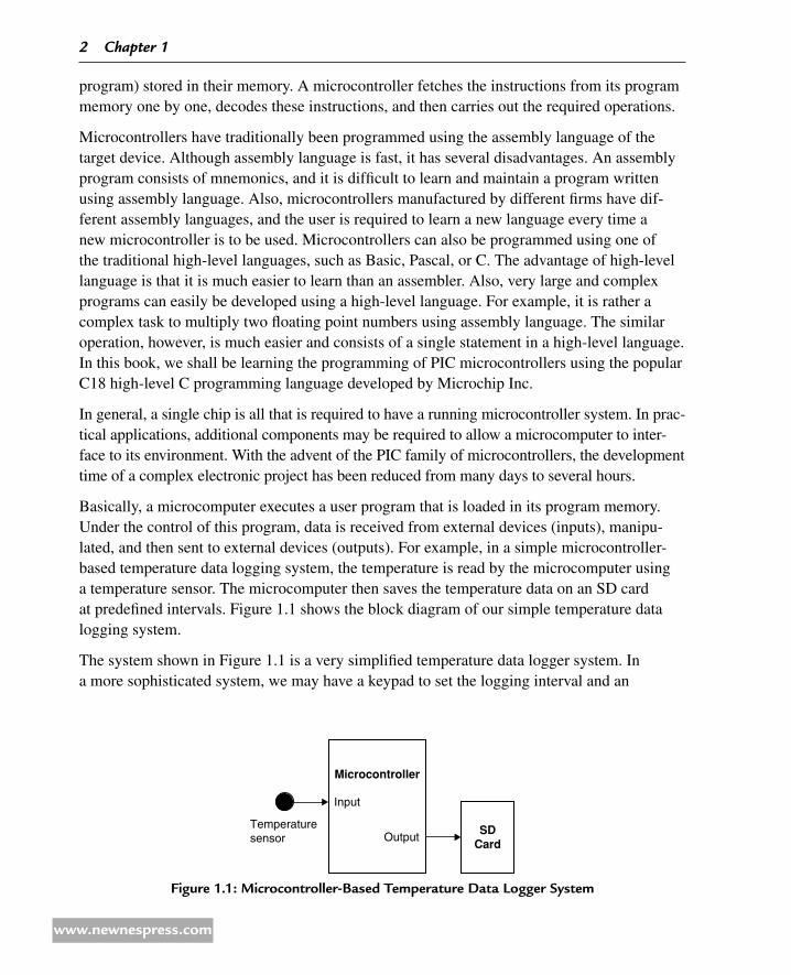
Basically, a microcomputer executes a user program that is loaded in its program memory. Under the control of this program, data is received from external devices (inputs), manipu-lated, and then sent to external devices (outputs). For example, in a simple microcontroller-based temperature data logging system, the temperature is read by the microcomputer using a temperature sensor. The microcomputer then saves the temperature data on an SD card at predefined intervals. Figure 1.1 shows the block diagram of our simple temperature data logging system.
The system shown in Figure 1.1 is a very simplified temperature data logger system. In a more sophisticated system, we may have a keypad to set the logging interval and an
Microcontroller
Temperaturesensor
SDCard
Input
Output
Figure 1.1: Microcontroller-Based temperature data Logger System
2 Chapter 1
www.newnespress.com

LCD to display the current temperature. Figure 1.2 shows the block diagram of this more sophisticated temperature data logger system.
We can make our design even more sophisticated (see Figure 1.3) by adding a real-time clock chip (RTC) to provide the absolute date and time information so that the data can be saved with date and time stamping. Also, the temperature readings can be sent to a PC every second for archiving and further processing. For example, a graph of the temperature change can be
Figure 1.2: temperature data Logger System with a Keypad and LCd
Microcontroller
Temperaturesensor
SDCard
Input
Output
Keypad
Input
LCD
Output
Figure 1.3: More Sophisticated temperature data Logger
Microcontroller
Temperaturesensor
SDCard
Input
Output
Keypad
Input
LCD
Output
PC
Output
RTC Input
Microcontroller systems 3
www.newnespress.com

plotted on the PC. As you can see, because the microcontrollers are programmable, it is very easy to make the final system as simple or as complicated as we like.
A microcontroller is a very powerful electronic device that allows a designer to create sophisticated I/O data manipulation under program control. Microcontrollers are classified by the number of bits they process. Eight-bit microcontrollers are the most popular ones and are used in most microcontroller-based monitoring and control applications. Microcontrollers of 16 and 32 bits are much more powerful but usually more expensive and not required in many small-to-medium-size, general-purpose applications where microcontrollers are generally used.
The simplest microcontroller architecture consists of a microprocessor, program and data memory, and I/O circuitry. The microprocessor itself consists of a central processing unit (CPU) and the control unit (CU). The CPU is the brain of the microprocessor, where all the arithmetic and logic operations are performed. The CU controls the internal operations of the microprocessor and sends out control signals to other parts of the microprocessor to carry out the required instructions.
Memory is an important part of a microcontroller system. Depending upon the type used, we can classify memory into two groups: program memory and data memory. Program memory stores the application program written by the programmer and is usually nonvolatile; i.e., data is not lost after the removal of power. Data memory is where the temporary data used in a program is stored and is usually volatile; i.e., data is lost after the removal of power.
There are basically six types of memory, as summarized below.
121 Random Access Memory
Random access memory (RAM) is a general-purpose memory that usually stores the user data in a program. RAM is volatile in the sense that it cannot retain data in the absence of power; i.e., data is lost after the removal of power. The RAM in a system is either static RAM (SRAM) or dynamic RAM (DRAM). The SRAMs are fast, with access time in the range of a few nanoseconds, which makes them ideal memory chips in com-puter applications. DRAMs are slower and because they are capacitor based they require refreshing every several milliseconds. DRAMs have the advantage that their power consumption is less than that of SRAMs. Most microcontrollers have some amount of internal RAM, commonly 256 bytes, although some microcontrollers have more and some have less. For example, the PIC18F452 microcontroller has 1536 bytes of RAM, which should be enough for most microcontroller-based applications. In most microcontroller systems, it is possible to extend the amount of RAM by adding external memory chips if desired.
4 Chapter 1
www.newnespress.com

122 Read Only Memory
Read only memory (ROM) is a type of memory that usually holds the application program or fixed user data. ROM is nonvolatile. If power is removed from ROM and then reapplied, the original data will still be there. ROMs are programmed at the factory during the manufac-turing process and their content cannot be changed by the user. ROMs are only useful if you have developed a microcontroller-based application and wish to order several thousand microcontroller chips preprogrammed with this program.
123 Programmable Read Only Memory
Programmable read only memory (PROM) is a type of ROM that can be programmed in the field, often by the end user, using a device called a PROM programmer. PROM is used to store an application program or constant data. Once a PROM has been programmed, its con-tents cannot be changed again. PROMs are usually used in low production applications where only several such memories are required.
124 Erasable Programmable Read Only Memory
Erasable programmable read only memory (EPROM) is similar to ROM, but the EPROM can be programmed using a suitable programming device. EPROMs have a small clear glass window on top of the chip where the data can be erased under strong ultraviolet light. Once the memory is programmed, the window should be covered with dark tape to prevent acci-dental erasure of the data. An EPROM must be erased before it can be reprogrammed. Many development versions of microcontrollers are manufactured with EPROMs where the user program can be stored. These memories are erased and reprogrammed until the user is satis-fied with the program. Some versions of EPROMs, known as one time programmable (OTP) EPROMs, can be programmed using a suitable programmer device, but these memories cannot be erased. OTP memories cost much less than EPROMs. OTP is useful after a project has been developed completely, and it is required to make many copies of the final program memory.
125 Electrically Erasable Programmable Read Only Memory
Electrically erasable programmable read only memory (EEPROM) is a nonvolatile memory. These memories can be erased and can also be reprogrammed using suitable programming devices. EEPROMs are used to save constant data, such as configuration information, maxi-mum and minimum values of a measurement, and identification data. Some microcontrollers have built-in EEPROMs. For example, PIC18F452 contains a 256-byte EEPROM where each byte can be programmed and erased directly by applications software. EEPROMs are usually very slow. The cost of an EEPROM chip is much higher than that of an EPROM chip.
Microcontroller systems 5
www.newnespress.com

126 Flash EEPROM
Flash EEPROM is another version of EEPROM type memory. This memory has become popular in microcontroller applications and is used to store the user program. Flash EEPROM is nonvolatile and is usually very fast. The data can be erased and then reprogrammed using a suitable programming device. Some microcontrollers have only 1K of flash EEPROM, while some others have 32 K or more. The PIC18F452 microcontroller has 32 KB of flash memory.
1.3 Microcontroller Features
Microcontrollers from different manufacturers have different architectures and different capabilities. Some may suit a particular application while others may be totally unsuitable for the same application. Some of the hardware features of microcontrollers in general are described in this section.
131 Buses
The connections between various blocks of a computer system are called buses. A bus is a common set of wires that carry a specific type of information. In general, every computer system has three buses: address bus, data bus, and control bus.
An address bus carries the address information in a computer system. It is a unidirectional bus having 16 bits in small computer systems and 32 or more bits in larger systems. An address bus usually carries the memory addresses from the CPU to the memory chips. This bus is also used to carry the I/O addresses in many computer systems.
A data bus carries the data in a computer system. It is a bidirectional bus having 8 bits in small systems and 14, 16, 32, or even more bits in larger systems. A data bus carries the memory data from the CPU to the memory chips. In addition, data is carried to other parts of a computer via the data bus.
The control bus is usually a smaller bus and is used to provide control signals to most parts of a computer system. For example, memory read and write control signals are carried by the control bus.
132 supply Voltage
Most microcontrollers operate with the standard logic voltage of +5 V. Some microcontro llers can operate at as low as +2.7 V and some will tolerate +6 V without any problems. You should check the manufacturers’ data sheets about the allowed limits of the power supply voltage. For example, PIC18F452 microcontrollers can operate with a power supply +2 to +5.5 V.
6 Chapter 1
www.newnespress.com

A voltage regulator circuit is usually used to obtain the required power supply voltage when the device is to be operated from a mains adaptor or batteries. For example, a 5-V regulator is required if the microcontroller is to be operated using a 9-V battery.
133 The Clock
All microcontrollers require a clock (or an oscillator) to operate. The clock is usually pro-vided by connecting external timing devices to the microcontroller. Most microcontrollers will generate clock signals when a crystal and two small capacitors are connected. Some will operate with resonators or external resistor-capacitor pair. Some microcontrollers have built-in timing circuits and they do not require any external timing components. If the appli-cation is not time sensitive, then external or internal (if available) resistor-capacitor timing components should be used to lower the costs.
An instruction is executed by fetching it from the memory and then decoding it. This usually takes several clock cycles and is known as the instruction cycle. In PIC microcontrollers, an instruction cycle takes four clock periods. Thus, the microcontroller is actually operated at a clock rate, which is a quarter of the actual oscillator frequency. For example, in a PIC microcontroller operating at 4-MHz clock, the instruction cycle time is only 1 µs (frequency of 1 MHz). The PIC18F series of microcontrollers can operate with clock frequencies up to 40 MHz.
134 Timers
Timers are important parts of any microcontroller. A timer is basically a counter, which is driven either by an external clock pulse or by the internal oscillator of the microcontroller. A timer can be 8 or 16 bits wide. Data can be loaded into a timer under program control and the timer can be stopped or started by program control. Most timers can be configured to generate an interrupt when they reach a certain count (usually when they overflow). The interrupt can be used by the user program to carry out accurate timing-related operations inside the microcontroller. The PIC18F series of microcontrollers have at least three timers. For example, the PIC18F452 microcontroller has three built-in timers.
Some microcontrollers offer capture and compare facilities where a timer value can be read when an external event occurs or the timer value can be compared to a preset value and an interrupt generated when this value is reached. Most PIC18F microcontrollers have at least two capture and compare modules.
135 Watchdog
Most microcontrollers have at least one watchdog facility. The watchdog is basically a timer that is normally refreshed by the user program, and a reset occurs if the program fails to refresh the watchdog. The watchdog timer is used to detect serious problems in programs,
Microcontroller systems 7
www.newnespress.com
such as the program being in an endless loop. A watchdog is a safety feature that prevents runaway software and stops the microcontroller from executing meaningless and unwanted code. Watchdog facilities are commonly used in real-time systems where it is required to regularly check the successful termination of one or more activities.
136 Reset Input
A reset input is used to reset a microcontroller externally. Resetting puts the microcontro ller into a known state such that the program execution starts usually from address 0 of the pro-gram memory. An external reset action is usually achieved by connecting a push-button switch to the reset input such that the microcontroller can be reset when the switch is pressed.
137 Interrupts
Interrupts are very important concepts in microcontrollers. An interrupt causes the microcon-troller to respond to external and internal (e.g., a timer) events very quickly. When an inter-rupt occurs, the microcontroller leaves its normal flow of program execution and jumps to a special part of the program known as the interrupt service routine (ISR). The program code inside the ISR is executed and upon return from the ISR the program resumes its normal flow of execution.
The ISR starts from a fixed address of the program memory. This address is known as the inter-rupt vector address. Some microcontrollers with multi-interrupt features have just one interrupt vector address, while some others have unique interrupt vector addresses, one for each interrupt source. Interrupts can be nested such that a new interrupt can suspend the execution of another interrupt. Another important feature of a microcontroller with multi-interrupt capability is that different interrupt sources can be given different levels of priority. For example, the PIC18F series of microcontrollers have low-priority and high-priority interrupt levels.
138 Brown-Out Detector
Brown-out detectors are also common in many microcontrollers, and they reset a micro-controller if the supply voltage falls below a nominal value. Brown-out detectors are safety features, and they can be employed to prevent unpredictable operation at low voltages, especially to protect the contents of EEPROM type memories if the supply voltage falls.
139 A/D Converter
An A/D converter is used to convert an analog signal like voltage to digital form so that it can be read and processed by a microcontroller. Some microcontrollers have built-in A/D converters. It is also possible to connect an external A/D converter to any type of
8 Chapter 1
www.newnespress.com

microcontroller. A/D converters are usually 8–10 bits having 256–1024 quantization levels. Most PIC microcontrollers with A/D features have multiplexed A/D converters where more than one analog input channel is provided. For example, the PIC18F452 microcontroller has 10-bit, 8-channel A/D converters.
The A/D conversion process must be started by the user program and it may take several hundreds of microseconds for a conversion to complete. A/D converters usually generate interrupts when a conversion is complete so that the user program can read the converted data quickly.
A/D converters are very useful in control and monitoring applications because most sensors (e.g., temperature sensor, pressure sensor, and force sensor) produce analog output voltages that cannot be read by a microcontroller without an A/D converter.
1310 serial I/O
Serial communication (also called RS232 communication) enables a microcontroller to communicate with other devices using the serial RS232 communication protocol. For example, a microcontroller can be connected to another microcontroller or to a PC and exchange data using the serial communication protocol. Some microcontrollers have built-in hardware called universal synchronous-asynchronous receiver-transmitter (USART) to implement a serial communication interface. The baud rate and the data format can usually be selected by the user program. If serial I/O hardware is not provided, it is easy to develop software to implement the serial data communication using any I/O pin of a microcontroller. The PIC18F series of microcontrollers have built-in USART modules.
Some microcontrollers (e.g., PIC18F series) incorporate a serial peripheral interface (SPI) or an integrated interconnect (I2C) hardware bus interface. These enable a microcontroller to interface to other compatible devices easily.
1311 EEPROM Data Memory
EEPROM type data memory is also very common in many microcontrollers. The advantage of an EEPROM is that the programmer can store nonvolatile data in such a memory and can also change this data whenever required. For example, in a temperature monitoring appli-cation, the maximum and the minimum temperature readings can be stored in an EEPROM. Then, if the power supply is removed for whatever reason, the values of the latest readings will still be available in the EEPROM. The PIC18F452 microcontroller has 256 bytes of EEPROM. Some other members of the family have more (e.g., PIC18F6680 has 1024 bytes) EEPROMs.
Microcontroller systems 9
www.newnespress.com

1312 LCD Drivers
LCD drivers enable a microcontroller to be connected to an external LCD display directly. These drivers are not common because most of the functions they provide can be implemented in the software. For example, the PIC18F6490 microcontroller has a built-in LCD driver module.
1313 Analog Comparator
Analog comparators are used where it is required to compare two analog voltages. Although these circuits are implemented in most high-end PIC microcontrollers, they are not common in other microcontrollers. The PIC18F series of microcontrollers have built-in analog compa-rator modules.
1314 Real-Time Clock
Real-time clock (RTC) enables a microcontroller to have absolute date and time information continuously. Built-in real-time clocks are not common in most microcontrollers because they can easily be implemented by either using a dedicated RTC or by writing a program.
1315 sleep Mode
Some microcontrollers (e.g., PIC) offer built-in sleep modes where executing this instruction puts the microcontroller into a mode where the internal oscillator is stopped and the power consumption is reduced to an extremely low level. The main reason for using the sleep mode is to conserve the battery power when the microcontroller is not doing anything useful. The microcontroller usually wakes up from the sleep mode by external reset or by a watchdog time-out.
1316 Power-on Reset
Some microcontrollers (e.g., PIC) have built-in power-on reset circuits, which keep the micro-controller in reset state until all the internal circuitry has been initialized. This feature is very useful as it starts the microcontroller from a known state on power-up. An external reset can also be provided where the microcontroller can be reset when an external button is pressed.
1317 Low-Power Operation
Low-power operation is especially important in portable applications where the microcontroller-based equipment is operated from batteries. Some microcontrollers (e.g., PIC) can operate with less than 2 mA at a 5-V supply and approximately 15 μA at a 3-V supply. Some other microcontrollers, especially microprocessor-based systems where there could be several chips, may consume several hundred milliamperes or even more.
10 Chapter 1
www.newnespress.com
1318 Current sink/source Capability
This is important if the microcontroller is to be connected to an external device that may draw large current for its operation. PIC microcontrollers can source and sink 25 mA of current from each output port pin. This current is usually sufficient to drive light-emitting diodes (LEDs), small lamps, buzzers, small relays, etc. The current capability can be increased by connecting external transistor switching circuits or relays to the output port pins.
1319 UsB Interface
USB is currently a very popular computer interface specification used to connect various peripheral devices to computers and microcontrollers. Some PIC microcontrollers provide built-in USB modules. For example, PIC18F2X50 has built-in USB interface capabilities.
1320 Motor Control Interface
Some PIC microcontrollers (e.g., PIC18F2X31) provide motor control interface.
1321 Controller Area Network Interface
Controller area network (CAN) bus is a very popular bus system used mainly in automation applications. Some PIC18F series of microcontrollers (e.g., PIC18F4680) provide CAN inter-face capabilities.
1322 Ethernet Interface
Some PIC microcontrollers (e.g., PIC18F97J60) provide Ethernet interface capabilities. Such microcontrollers can easily be used in network-based applications.
1323 ZigBee Interface
ZigBee is an interface similar to Bluetooth and is used in low-cost wireless home automation applications. Some PIC18F series of microcontrollers provide ZigBee interface capabilities, making the design of such wireless systems very easy.
1.4 Microcontroller architectures
Usually two types of architecture are used in microcontrollers (see Figure 1.4): Von Neu-mann architecture and Harvard architecture. Von Neumann architecture is used by a large percentage of microcontrollers, where all memory space is on the same bus and instruction and data use the same bus. In the Harvard architecture (used by the PIC microcontrollers),
Microcontroller systems 11
www.newnespress.com

code and data are on separate buses, and this allows the code and data to be fetched simul-taneously, resulting in an improved performance.
141 Reduced Instruction set Computer and Complex Instruction set Computer
Reduced instruction set computer (RISC) and complex instruction set computer (CISC) refer to the instruction set of a microcontroller. In an 8-bit RISC microcontroller, data is 8 bits wide but the instruction words are more than 8 bits wide (usually 12, 14, or 16 bits), and the instructions occupy one word in the program memory. Thus, the instructions are fetched and executed in one cycle, resulting in an improved performance.
In a CISC microcontroller, both data and instructions are 8 bits wide. CISC microcontrollers usually have over 200 instructions. Data and code are on the same bus and cannot be fetched simultaneously.
1.5 Choosing a PiC Microcontroller
Choosing a microcontroller for an application requires taking into account the following factors:
Microcontroller speed •
The number of I/O pins required •
The peripheral devices required (e.g., USART and A/D converter) •
The memory size (RAM, flash, EEPROM, etc.) •
Power consumption •
Physical size •
Figure 1.4: Von Neumann and harvard architectures
(b) Harvard architecture (a) Von Neumann architecture
CPU Data
memoryProgrammemory
ProgrammemoryCPU
12 Chapter 1
www.newnespress.com
1.6 Number Systems
The efficient use of a microprocessor or a microcontroller requires a working knowledge of binary, decimal, and hexadecimal numbering systems. This section provides a background for those who are unfamiliar with these numbering systems and who do not know how to convert from one number system to another one.
Number systems are classified according to their bases. The numbering system used in everyday life is base 10 or the decimal number system. The most commonly used numbering system in microprocessor and microcontroller applications is base 16 or hexadecimal. In addition, base 2 (binary) or base 8 (octal) number systems are also used.
161 Decimal Number system
As you all know, the numbers in this system are 0, 1, 2, 3, 4, 5, 6, 7, 8, and 9. We can use the subscript 10 to indicate that a number is in decimal format. For example, we can show the decimal number 235 as 23510.
In general, a decimal number is represented as follows:
an × 10n + an−1 × 10n−1 + an−2 × 10 n−2 + … + a0 × 100
For example, decimal number 82510 can be shown as follows:
82510 = 8 × 10² + 2 × 101 + 5 × 100
Similarly, decimal number 2610 can be shown as follows:
2610 = 2 × 101 + 6 × 100
or
335910 = 3 × 10³ + 3 × 10² + 5 × 101 + 9 × 100
162 Binary Number system
In the binary number system, there are two numbers: 0 and 1. We can use the subscript 2 to indicate that a number is in binary format. For example, we can show binary number 1011 as 10112.
In general, a binary number is represented as follows:
an × 2n + an−1 × 2n−1 + an−2 × 2n−2 + … + a0 × 20
For example, binary number 11102 can be shown as follows:
11102 = 1 × 23 + 1 × 22 + 1 × 21 + 0 × 20
Microcontroller systems 13
www.newnespress.com

Similarly, binary number 100011102 can be shown as follows:
100011102 = 1 × 27 + 0 × 26 + 0 × 25 + 0 × 24 + 1 × 23 + 1 × 22 + 1 × 21 + 0 × 20
163 Octal Number system
In the octal number system, the valid numbers are 0, 1, 2, 3, 4, 5, 6, and 7. We can use the subscript 8 to indicate that a number is in octal format. For example, we can show octal number 23 as 238.
In general, an octal number is represented as follows:
an × 8n + an−1 × 8n−1 + an−2 × 8n−2 + … + a0 × 80
For example, octal number 2378 can be shown as follows:
2378 = 2 × 82 + 3 × 81 + 7 × 80
Similarly, octal number 17778 can be shown as follows:
17778 = 1 × 83 + 7 × 82 + 7 × 81 + 7 × 80
164 Hexadecimal Number system
In the hexadecimal number system, the valid numbers are 0, 1, 2, 3, 4, 5, 6, 7, 8, 9, A, B, C, D, E, and F. We can use the subscript 16 or H to indicate that a number is in hexadecimal format. For example, we can show hexadecimal number 1F as 1F16 or as 1FH.
In general, a hexadecimal number is represented as follows:
an × 16n + an−1 × 16n−1 + an−2 × 16n−2 + … + a0 × 160
For example, hexadecimal number 2AC16 can be shown as follows:
2AC16 = 2 × 162 + 10 × 161 + 12 × 160
Similarly, hexadecimal number 3FFE16 can be shown as follows:
3FFE16 = 3 × 163 + 15 × 162 + 15 × 161 + 14 × 160
1.7 Converting Binary Numbers into decimal
To convert a binary number into decimal, write the number as the sum of the powers of 2.
14 Chapter 1
www.newnespress.com
example 1. 1
Convert binary number 10112 into decimal.
solution
Write the number as the sum of the powers of 2:
10112 = 1 × 23 + 0 × 22 + 1 × 21 + 1 × 20
= 8 + 0 + 2 + 1
= 11
or 10112 = 1110.
example 1. 2
Convert binary number 110011102 into decimal.
solution
Write the number as the sum of the powers of 2:
110011102 = 1 × 27 + 1 × 26 + 0 × 25 + 0 × 24 + 1 × 23 + 1 × 22 + 1 × 21 + 0 × 20
= 128 + 64 + 0 + 0 + 8 + 4 + 2 + 0
= 206
or 110011102 = 20610.
Table 1.1 shows the binary equivalent of decimal numbers from 0 to 31.
table 1.1: Binary equivalent of decimal Numbers
decimal Binary decimal Binary
0 00000000 16 00010000
1 00000001 17 00010001
2 00000010 18 00010010
3 00000011 19 00010011
4 00000100 20 00010100
—cont’d
Microcontroller systems 15
www.newnespress.com

1.8 Converting decimal Numbers into Binary
To convert a decimal number into binary, divide the number repeatedly by 2 and take the remainders. The first remainder is the least significant digit (LSD) and the last remainder is the most significant digit (MSD).
example 1.3
Convert decimal number 2810 into binary.
solution
Divide the number by 2 repeatedly and take the remainders:
28/2 → 14 Remainder 0 (LSD)
14/2 → 7 Remainder 0
7/2 → 3 Remainder 1
3/2 → 1 Remainder 1
1/2 → 0 Remeinder 1 (MSD)
The required binary number is 111002.
decimal Binary decimal Binary
5 00000101 21 00010101
6 00000110 22 00010110
7 00000111 23 00010111
8 00001000 24 00011000
9 00001001 25 00011001
10 00001010 26 00011010
11 00001011 27 00011011
12 00001100 28 00011100
13 00001101 29 00011101
14 00001110 30 00011110
15 00001111 31 00011111
table 1.1: Binary equivalent of decimal Numbers —cont’d
16 Chapter 1
www.newnespress.com

example 1.4
Convert decimal number 6510 into binary.
solution
Divide the number by 2 repeatedly and take the remainders:
65/2 → 32 Remainder 1 (LSD)
32/2 → 16 Remainder 0
16/2 → 8 Remainder 0
8/2 → 4 Remainder 0
4/2 → 2 Remainder 0
2/2 → 1 Remainder 0
1/2 → 0 Remainder 1 (MSD)
The required binary number is 10000012.
example 1.5
Convert decimal number 12210 into binary.
solution
Divide the number by 2 repeatedly and take the remainders:
122/2 → 61 Remainder 0 (LSD)
61/2 → 30 Remainder 1
30/2 → 15 Remainder 0
15/2 → 7 Remainder 1
7/2 → 3 Remainder 1
3/2 → 1 Remainder 1
1/2 → 0 Remainder 1 (MSD)
The required binary number is 11110102.
Microcontroller systems 17
www.newnespress.com

1.9 Converting Binary Numbers into hexadecimal
To convert a binary number into hexadecimal, arrange the number in groups of four and find the hexadecimal equivalent of each group. If the number cannot be divided exactly into groups of four, insert zeroes to the left-hand side of the number.
example 1.6
Convert binary number 100111112 into hexadecimal.
solution
First, divide the number into groups of four and then find the hexadecimal equivalent of each group:
10011111 = 1001 1111
The required hexadecimal number is 9F16.
example 1.7
Convert binary number 11101111000011102 into hexadecimal.
solution
First, divide the number into groups of four and then find the equivalent of each group:
1110111100001110 = 1110 1111 0000 1110
The required hexadecimal number is EF0E16.
example 1. 8
Convert binary number 1111102 into hexadecimal.
solution
Because the number cannot be divided exactly into groups of four, we have to insert zeroes to the left of the number:
111110 = 0011 1110
The required hexadecimal number is 3E16.
9 F
E F 0 E
3 E
18 Chapter 1
www.newnespress.com

Table 1.2 shows the hexadecimal equivalent of decimal numbers 0 to 31.
table 1.2: hexadecimal equivalent of decimal Numbers
decimal hexadecimal decimal hexadecimal
0 0 16 10
1 1 17 11
2 2 18 12
3 3 19 13
4 4 20 14
5 5 21 15
6 6 22 16
7 7 23 17
8 8 24 18
9 9 25 19
10 A 26 1A
11 B 27 1B
12 C 28 1C
13 D 29 1D
14 E 30 1E
15 F 31 1F
1.10 Converting hexadecimal Numbers into Binary
To convert a hexadecimal number into binary, write the 4-bit binary equivalent of each hexadecimal digit.
example 1.9
Convert hexadecimal number A916 into binary.
solution
Writing the binary equivalent of each hexadecimal digit
A = 10102 9 = 10012
The required binary number is 101010012.
Microcontroller systems 19
www.newnespress.com

example 1.10
Convert hexadecimal number FE3C16 into binary.
solution
Writing the binary equivalent of each hexadecimal digit
F = 11112 E = 11102 3 = 00112 C = 11002
The required binary number is 11111110001111002.
1.11 Converting hexadecimal Numbers into decimal
To convert a hexadecimal number into decimal, we have to calculate the sum of the powers of 16 of the number.
example 1.11
Convert hexadecimal number 2AC16 into decimal.
solution
Calculating the sum of the powers of 16 of the number:
2AC16 = 2 × 162 + 10 × 161 + 12 × 160
= 512 + 160 + 12
= 684
The required decimal number is 68410.
example 1.12
Convert hexadecimal number EE16 into decimal.
solution
Calculating the sum of the powers of 16 of the number
EE16 = 14 × 161 + 14 × 160
= 224 + 14
= 238
The required decimal number is 23810.
20 Chapter 1
www.newnespress.com

1.12 Converting decimal Numbers into hexadecimal
To convert a decimal number into hexadecimal, divide the number repeatedly by 16 and take the remainders. The first remainder is the LSD and the last remainder is the MSD.
exa mple 1.13
Convert decimal number 23810 into hexadecimal.
solution
Dividing the number repeatedly by 16
238/16 → 14 Remainder 14 (E) (LSD)
14/16 → 0 Remainder 14 (E) (MSD)
The required hexadecimal number is EE16.
example 1.14
Convert decimal number 68410 into hexadecimal.
solution
Dividing the number repeatedly by 16
684/16 → 42 Remainder 12 (C) (LSD)
42/16 → 2 Remainder 10 (A)
2/16 → 0 Remainder 2 (MSD)
The required hexadecimal number is 2AC16.
1.13 Converting Octal Numbers into decimal
To convert an octal number into decimal, calculate the sum of the powers of 8 of the number.
Microcontroller systems 21
www.newnespress.com

example 1.15
Convert octal number 158 into decimal.
solution
Calculating the sum of the powers of 8 of the number
158 = 1 × 81 + 5 × 80
= 8 + 5
= 13
The required decimal number is 1310.
example 1.16
Convert octal number 2378 into decimal.
solution
Calculating the sum of the powers of 8 of the number
2378 = 2 × 82 + 3 × 81 + 7 × 80
= 128 + 24 + 7
= 159
The required decimal number is 15910.
1.14 Converting decimal Numbers into Octal
To convert a decimal number into octal, divide the number repeatedly by 8 and take the remainders. The first remainder is the LSD and the last remainder is the MSD.
example 1. 17
Convert decimal number 15910 into octal.
solution
Dividing the number repeatedly by 8
22 Chapter 1
www.newnespress.com

159/8 → 19 Remainder 7 (LSD)
19/8 → 2 Remainder 3
2/8 → 0 Remainder 2 (MSD)
The required octal number is 2378.
e xample 1.18
Convert decimal number 46010 into octal.
solution
Dividing the number repeatedly by 8
460/8 → 57 Remainder 4 (LSD)
57/8 → 7 Remainder 1
7/8 → 0 Remainder 7 (MSD)
The required octal number is 7148.
Table 1.3 shows the octal equivalent of decimal numbers 0–31.
table 1.3: Octal equivalent of decimal Numbers
decimal Octal decimal Octal
0 0 16 20
1 1 17 21
2 2 18 22
3 3 19 23
4 4 20 24
5 5 21 25
6 6 22 26
7 7 23 27
8 10 24 30
9 11 25 31
10 12 26 32
11 13 27 33
12 14 28 34
13 15 29 35
14 16 30 36
15 17 31 37
Microcontroller systems 23
www.newnespress.com
1.15 Converting Octal Numbers into Binary
To convert an octal number into binary, write the 3-bit binary equivalent of each octal digit.
example 1.19
Convert octal number 1778 into binary.
solution
Write the binary equivalent of each octal digit:
1 = 0012 7 = 1112 7 = 1112
The required binary number is 0011111112.
example 1.20
Convert octal number 758 into binary.
solution
Write the binary equivalent of each octal digit:
7 = 1112 5 = 1012
The required binary number is 1111012.
1.16 Converting Binary Numbers into Octal
To convert a binary number into octal, arrange the number in groups of three and write the octal equivalent of each digit.
example 1.21
Convert binary number 1101110012 into octal.
solution
Arranging in groups of three
110111001 = 1160 11
71 00
11
The required octal number is 6718.
24 Chapter 1
www.newnespress.com
1.17 Negative Numbers
The most significant bit of a binary number is usually used as the sign bit. By convention, for positive numbers this bit is 0 and for negative numbers this bit is 1. Table 1.4 shows the 4-bit positive and negative numbers. The largest positive and negative numbers are +7 and −8, respectively.
To convert a positive number into negative, take the complement of the number and add 1. This process is also called the 2’s complement of the number.
example 1.22
Write decimal number −6 as a 4-bit number.
solution
First, write the number as a positive number, then find the complement and add 1:
0110 +6
1001 complement
1 add 1_____
1010 which is −6
table 1.4: Four-Bit Positive and Negative Numbers
Binary Numbers decimal equivalent
0111 +7
0110 +6
0101 +5
0100 +4
0011 +3
0010 +2
0001 +1
0000 0
1111 −1
1110 −2
1101 −3
1100 −4
1011 −5
1010 −6
1001 −7
1000 −8
Microcontroller systems 25
www.newnespress.com
example 1.23
Write decimal number −25 as an 8-bit number.
solution
First, write the number as a positive number, then find the complement and add 1:
00011001 +25
11100110 complement
1 add 1_________
11100111 which is −25
1.18 adding Binary Numbers
The addition of binary numbers is similar to the addition of decimal numbers. Numbers in each column are added together with a possible carry from a previous column. The primitive addition operations are as follows:
0 + 0 = 0
0 + 1 = 1
1 + 0 = 1
1 + 1 = 10 generate a carry bit
1 + 1 + 1 = 11 generate a carry bit
Some examples are given below.
example 1.24
Find the sum of binary numbers 011 and 110.
solution
We can add these numbers as in the addition of decimal numbers:
011 First column: 1 + 0 = 1
+ 110 Second column: 1 + 1 = 0 and a carry bit_____
Third column: 1 + 1 = 10 1001
26 Chapter 1
www.newnespress.com

example 1.25
Find the sum of binary numbers 01000011 and 00100010.
solution
We can add these numbers as in the addition of decimal numbers:
01000011 First column: 1 + 0 = 1
+ 00100010 Second column: 1 + 1 = 10___________
Third column: 0 + carry = 1 01100101
Fourth column: 0 + 0 = 0
Fifth column: 0 + 0 = 0
Sixth column: 0 + 1 = 1
Seventh column: 1 + 0 = 1
Eighth column: 0 + 0 = 0
1.19 Subtracting Binary Numbers
To subtract two binary numbers, convert the number to be subtracted into negative and then add the two numbers.
example 1.26
Subtract binary number 0010 from 0110.
solution
First, let’s convert the number to be subtracted into negative:
0010 number to be subtracted
1101 complement
1 add 1____
1110
Microcontroller systems 27
www.newnespress.com

Now, add the two numbers:
0110
+ 1110_______
0100
Because we are using 4 bits only, we cannot show the carry bit.
1.20 Multiplication of Binary Numbers
Multiplication of two binary numbers is same as the multiplication of decimal numbers. The four possibilities are as follows:
0 × 0 = 0
0 × 1 = 0
1 × 0 = 0
1 × 1 = 1
Some examples are given below.
example 1.27
Multiply the two binary numbers 0110 and 0010.
solution
Multiplying the numbers
0110
0010____
0000
0110
0000
0000______
001100 or 1100
In this example, 4 bits are needed to show the final result.
28 Chapter 1
www.newnespress.com

e xample 1.28
Multiply binary numbers 1001 and 1010.
solution
Multiplying the numbers1001
1010_____
0000
1001
0000
1001_______
1011010
In this example, 7 bits are required to show the final result.
1.21 division of Binary Numbers
The division of binary numbers is similar to the division of decimal numbers. An example is given below.
example 1.29
Divide binary number 1110 by binary number 10.
solution
Dividing the numbers111
10 1110
10__
11
10__
10
10__
00
gives the result 1112.
Microcontroller systems 29
www.newnespress.com

1.22 Floating Point Numbers
Floating point numbers are used to represent noninteger fractional numbers and are used in most engineering and technical calculations, for example, 3.256, 2.1, and 0.0036. The most commonly used floating point standard is the IEEE standard. According to this standard, floating point numbers are represented with 32 bits (single precision) or 64 bits (double precision).
In this section, we will look at the format of 32-bit floating point numbers only and see how mathematical operations can be performed with such numbers.
According to the IEEE standard, 32-bit floating point numbers are represented as follows:
31 30 23 22 0
X XXXXXXXX XXXXXXXXXXXXXXXXXXXXXXX
↑ ↑ ↑ sign exponent mantissa
The most significant bit indicates sign of the number, where 0 indicates positive and 1 indicates negative.
The 8-bit exponent shows the power of the number. To make the calculations easy, the sign of the exponent is not shown, but instead excess 128 numbering system is used. Thus, to find the real exponent, we have to subtract 127 from the given exponent. For example, if the mantissa is “10000000,” the real value of the mantissa is 128 − 127 = 1.
The mantissa is 23 bits wide and represents the increasing negative powers of 2. For example, if we assume that the mantissa is “1110000000000000000000,” the value of this mantissa is calculated as follows: 2−1 + 2−2 + 2−3 = 7/8.
The decimal equivalent of a floating point number can be calculated using the following formula:
Number = (−1)s 2e − 127 1 ⋅ f,
where s = 0 for positive numbers, 1 for negative numbers, e = exponent (between 0 and 255), and f = mantissa.
As shown in the above formula, there is a hidden “1” before the mantissa; i.e., mantissa is shown as “1 · f.”
The largest and the smallest numbers in 32-bit floating point format are as follows:
30 Chapter 1
www.newnespress.com

The largest number
0 11111110 11111111111111111111111
This number is (2 − 2−23) 2127 or decimal 3.403 × 1038. The numbers keep their precision up to six digits after the decimal point.
The smallest number
0 00000001 00000000000000000000000
This number is 2−126 or decimal 1.175 × 10−38.
1.23 Converting a Floating Point Number into decimal
To convert a given floating point number into decimal, we have to find the mantissa and the exponent of the number and then convert into decimal as shown above.
Some examples are given here.
example 1.30
Find the decimal equivalent of the floating point number given below:
0 10000001 10000000000000000000000
solution
Here,
sign = positive
exponent = 129 − 127 = 2
mantissa = 2−1 = 0.5
The decimal equivalent of this number is +1.5 × 22 = +6.0.
Microcontroller systems 31
www.newnespress.com
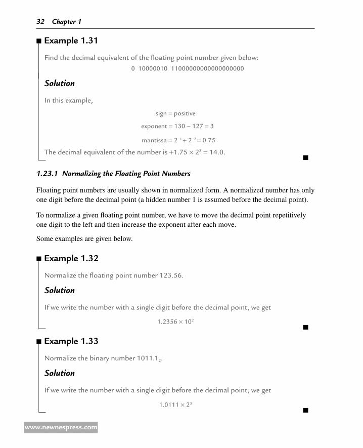
e xample 1.31
Find the decimal equivalent of the floating point number given below:
0 10000010 11000000000000000000
solution
In this example,
sign = positive
exponent = 130 − 127 = 3
mantissa = 2−1 + 2−2 = 0.75
The decimal equivalent of the number is +1.75 × 23 = 14.0.
1231 Normalizing the Floating Point Numbers
Floating point numbers are usually shown in normalized form. A normalized number has only one digit before the decimal point (a hidden number 1 is assumed before the decimal point).
To normalize a given floating point number, we have to move the decimal point repetitively one digit to the left and then increase the exponent after each move.
Some examples are given below.
example 1.32
Normalize the floating point number 123.56.
solution
If we write the number with a single digit before the decimal point, we get
1.2356 × 10²
example 1.33
Normalize the binary number 1011.12.
solution
If we write the number with a single digit before the decimal point, we get
1.0111 × 23
32 Chapter 1
www.newnespress.com

1232 Converting a Decimal Number into Floating Point
To convert a given decimal number into floating point, we have to carry out the following steps:
Write the number in binary •
Normalize the number •
Find the mantissa and the exponent •
Write the number as a floating point number •
Some examples are given below.
example 1.34
Convert decimal number 2.2510 into floating point.
solution
Writing the number in binary
2.2510 = 10 .012
Normalizing the number,
10.012 = 1.0012 × 21
Here, s = 0, e − 127 = 1 or e = 128, and f = 00100000000000000000000.
(Remember that a number 1 is assumed on the left-hand side, even though it is not shown in the calculation.) We can now write the required floating point number as follows:
s e f 0 10000000 (1)001 0000 0000 0000 0000 0000
or the required 32-bit floating point number is
01000000000100000000000000000000
example 1.35
Convert the decimal number 134.062510 into floating point.
solution
Writing the number in binary
134.062510 = 10000110.0001
Microcontroller systems 33
www.newnespress.com
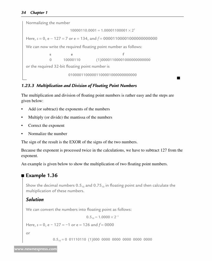
Normalizing the number
10000110.0001 = 1.00001100001 × 27
Here, s = 0, e − 127 = 7 or e = 134, and f = 00001100001000000000000
We can now write the required floating point number as follows:
s e f 0 10000110 (1)00001100001000000000000
or the required 32-bit floating point number is
01000011000001100001000000000000
1233 Multiplication and Division of Floating Point Numbers
The multiplication and division of floating point numbers is rather easy and the steps are given below:
Add (or subtract) the exponents of the numbers •
Multiply (or divide) the mantissa of the numbers •
Correct the exponent •
Normalize the number •
The sign of the result is the EXOR of the signs of the two numbers.
Because the exponent is processed twice in the calculations, we have to subtract 127 from the exponent.
An example is given below to show the multiplication of two floating point numbers.
example 1.36
Show the decimal numbers 0.510 and 0.7510 in floating point and then calculate the multiplication of these numbers.
solution
We can convert the numbers into floating point as follows:
0.510 = 1.0000 × 2−1
Here, s = 0, e − 127 = −1 or e = 126 and f = 0000
or
0.510 = 0 01110110 (1)000 0000 0000 0000 0000 0000
34 Chapter 1
www.newnespress.com

Similarly,
0.7510 = 1.1000 × 2−1
Here, s = 0, e = 126, and f = 1000
or
0.7510 = 0 01110110 (1)100 0000 0000 0000 0000 0000
Multiplying the mantissas, we get “(1)100 0000 0000 0000 0000 0000.” The sum of the exponents is 126 + 126 = 252. Subtracting 127 from the mantissa, we obtain 252 − 127 = 125. The EXOR of the signs of the numbers is 0. Thus, the result can be shown in floating point as follows:
0 01111101 (1)100 0000 0000 0000 0000 0000
The above number is equivalent to decimal 0.375 (0.5 × 0.75 = 0.375), which is the correct result.
1234 Addition and subtraction of Floating Point Numbers
The exponents of floating point numbers must be the same before they can be added or subtracted. The steps to add or subtract floating point numbers is as follows:
Shift the smaller number to the right until the exponents of both numbers are the same. •Increment the exponent of the smaller number after each shift.
Add (or subtract) the mantissa of each number as an integer calculation, without •considering the decimal points.
Normalize the obtained result. •
An example is given below.
example 1.37
Show decimal numbers 0.510 and 0.7510 in floating point and then calculate the sum of these numbers.
solution
As shown in Example 1.36, we can convert the numbers into floating point as follows:
0.510 = 0 01110110 (1)000 0000 0000 0000 0000 0000
Similarly,
0.7510 = 0 01110110 (1)100 0000 0000 0000 0000 0000
Microcontroller systems 35
www.newnespress.com

Because the exponents of both numbers are the same, there is no need to shift the smaller number. If we add the mantissa of the numbers without considering the decimal points, we get
(1)000 0000 0000 0000 0000 0000
(1)100 0000 0000 0000 0000 0000 _________________________________ +(10)100 0000 0000 0000 0000 0000
To normalize the number, we can shift it right by one digit and then increment its exponent. The resulting number is
0 01111111 (1)010 0000 0000 0000 0000 0000
The above floating point number is equal to decimal number 1.25, which is the sum of decimal numbers 0.5 and 0.75.
To convert floating point numbers into decimal and decimal numbers into floating point, the freely available program given in the following Web site can be used:
http://www.babbage.cs.qc.edu/IEEE-754/Decimal.html
1.24 Binary-Coded decimal Numbers
Binary-coded decimal (BCD) numbers are usually used in display systems like LCDs and seven-segment displays to show numeric values. BCD data is stored in either packed or unpacked forms. Packed BCD data is stored as two digits per byte and unpacked BCD data is stored as one digit per byte. Unpacked BCD data is usually returned from a keypad or a keyboard. The packed BCD is more frequently used, and this is the format described in the remainder of this section.
In packed BCD, each digit is a 4-bit number from 0 to 9. As an example, Table 1.5 shows the packed BCD numbers between 0 and 20.
table 1.5: Packed BCd Numbers Between 0 and 20
decimal BCd Binary
0 0000 0000
1 0001 0001
2 0010 0010
3 0011 0011
4 0100 0100
5 0101 0101
36 Chapter 1
www.newnespress.com
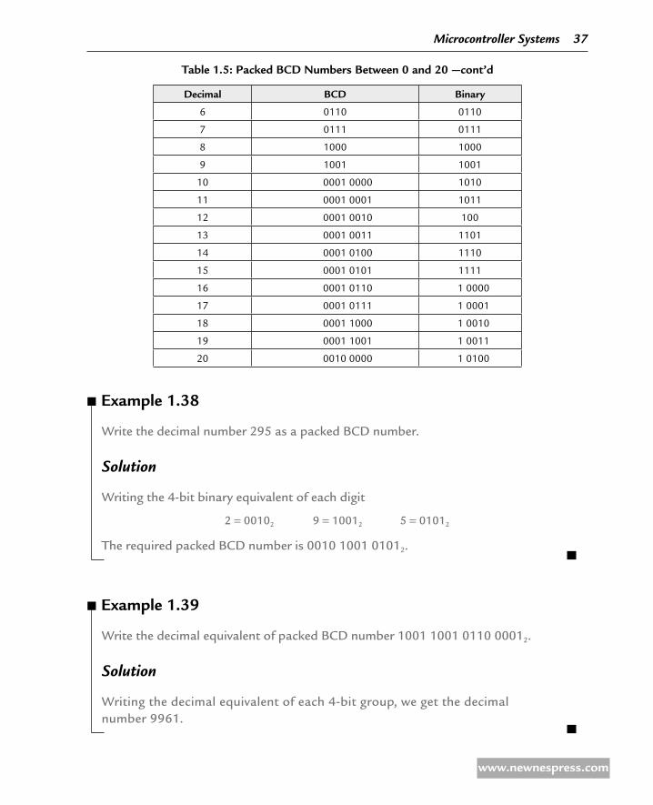
example 1.38
Write the decimal number 295 as a packed BCD number.
solution
Writing the 4-bit binary equivalent of each digit
2 = 00102 9 = 10012 5 = 01012
The required packed BCD number is 0010 1001 01012.
example 1.39
Write the decimal equivalent of packed BCD number 1001 1001 0110 00012.
solution
Writing the decimal equivalent of each 4-bit group, we get the decimal number 9961.
decimal BCd Binary
6 0110 0110
7 0111 0111
8 1000 1000
9 1001 1001
10 0001 0000 1010
11 0001 0001 1011
12 0001 0010 100
13 0001 0011 1101
14 0001 0100 1110
15 0001 0101 1111
16 0001 0110 1 0000
17 0001 0111 1 0001
18 0001 1000 1 0010
19 0001 1001 1 0011
20 0010 0000 1 0100
table 1.5: Packed BCd Numbers Between 0 and 20 —cont’d
Microcontroller systems 37
www.newnespress.com

1.25 Summary
This chapter has given an introduction to the microprocessor and microcontroller systems. The basic building blocks of microcontrollers have been described briefly. The chapter has also provided an introduction to various number systems, and has described how to convert a given number from one base into another base. The important topics of floating point numbers and floating point arithmetic have also been described with examples.
1.26 exercises
What is a microcontroller? What is a microprocessor? Explain the main differences 1. between a microprocessor and a microcontroller.
Give some example applications of microcontrollers around you. 2.
Where would you use an EPROM? 3.
Where would you use a RAM? 4.
Explain what types of memory are usually used in microcontrollers. 5.
What is an I/O port? 6.
What is an A/D converter? Give an example of use of this converter. 7.
Explain why a watchdog timer could be useful in a real-time system. 8.
What is serial I/O? Where would you use serial communication? 9.
Why is the current sinking/sourcing important in the specification of an output port pin?10.
What is an interrupt? Explain what happens when an interrupt is recognized by a 11. microcontroller.
Why is brown-out detection important in real-time systems?12.
Explain the differences between a RISC-based microcontroller and a CISC-based 13. microcontroller. What type of microcontroller is PIC?
Convert the following decimal numbers into binary:14. a) 23 b) 128 c) 255 d) 1023e) 120 f) 32000 g) 160 h) 250
Convert the following binary numbers into decimal:15. a) 1111 b) 0110 c) 11110000d) 00001111 e) 10101010 f) 10000000
38 Chapter 1
www.newnespress.com
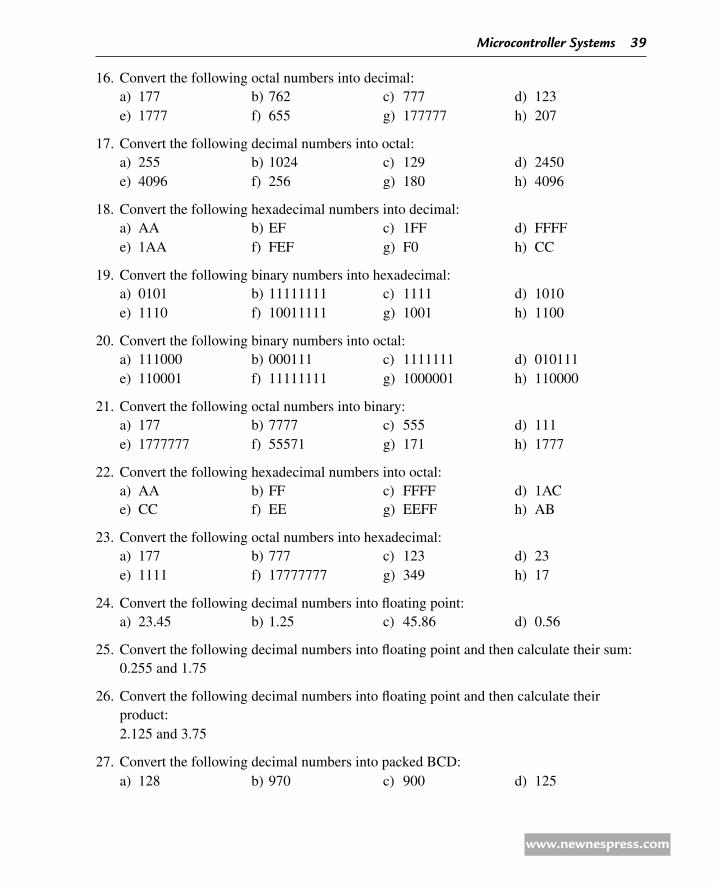
Convert the following octal numbers into decimal:16. a) 177 b) 762 c) 777 d) 123e) 1777 f) 655 g) 177777 h) 207
Convert the following decimal numbers into octal:17. a) 255 b) 1024 c) 129 d) 2450e) 4096 f) 256 g) 180 h) 4096
Convert the following hexadecimal numbers into decimal:18. a) AA b) EF c) 1FF d) FFFFe) 1AA f) FEF g) F0 h) CC
Convert the following binary numbers into hexadecimal:19. a) 0101 b) 11111111 c) 1111 d) 1010e) 1110 f) 10011111 g) 1001 h) 1100
Convert the following binary numbers into octal:20. a) 111000 b) 000111 c) 1111111 d) 010111e) 110001 f) 11111111 g) 1000001 h) 110000
Convert the following octal numbers into binary:21. a) 177 b) 7777 c) 555 d) 111e) 1777777 f) 55571 g) 171 h) 1777
Convert the following hexadecimal numbers into octal:22. a) AA b) FF c) FFFF d) 1ACe) CC f) EE g) EEFF h) AB
23. Convert the following octal numbers into hexadecimal:a) 177 b) 777 c) 123 d) 23e) 1111 f) 17777777 g) 349 h) 17
Convert the following decimal numbers into floating point:24. a) 23.45 b) 1.25 c) 45.86 d) 0.56
25. Convert the following decimal numbers into floating point and then calculate their sum:0.255 and 1.75
Convert the following decimal numbers into floating point and then calculate their 26. product:2.125 and 3.75
Convert the following decimal numbers into packed BCD:27. a) 128 b) 970 c) 900 d) 125
Microcontroller systems 39
www.newnespress.com
Convert the following decimal numbers into unpacked BCD:28. a) 128 b) 970 c) 900 d) 125
29. Convert the following packed BCD numbers into decimal:a) 0110 0011 b) 0111 0100 c) 0001 0111
40 Chapter 1
www.newnespress.com
ChaPter 2
PIC18F Microcontroller series
The PIC16 series of microcontrollers have been around for many years. Although they are excellent general-purpose microcontrollers, they have certain limitations. For example, the program and data memory capacities are limited, the stack is small, and the interrupt structure is primitive – all interrupt sources share the same interrupt vector. The PIC16 series of microcontrollers also do not provide direct support for advanced peripheral interfaces, such as USB and CAN bus, and it is rather complex to interface to such devices easily. The instruction set of these microcontrollers is also limited. For example, there are no instructions for multiplication or division and branching is rather simple and is made out of a combination of skip and goto instructions. Microchip Inc. has developed the PIC18 series of microcontrollers for high-pin-count, high-density, and complex applications.
Figure 2.1 shows the current PIC microcontroller family of products. At the lowest end of the family, we have the PIC10 microcontrollers, operating at approximately 5 MIPS and with small form factors, less memory, and a low cost. Then we have the PIC12 and PIC16 series of micro-controllers with midrange architectures, 5–8 MIPS operating performance, and reasonable size of memory. The microcontrollers of the PIC18 family are advanced high-performance devices, with 10–16 MIPS, and offer a large amount of memory with various on-chip peripheral support modules. As shown in Figure 2.1, the higher end of the family consists of 16-bit devices, such as the PIC24 and the dsPIC, and 32-bit devices, such as the dsPIC33 and the PIC32 series.
The PIC18 microcontroller family consists of three architectures: the standard PIC18F series, the PIC18J series, and the PIC18K series. PIC18J series are 10–12 MIPS, low-voltage, high-performance microcontrollers with integrated USB, Ethernet, or LCD. PIC18K series are 16 MIPS, high-performance, and low-power devices.
In this book, we shall be using the standard PIC18F series of microcontrollers. The PIC18F microcontrollers can be used in cost-efficient solutions for general-purpose applications written in C, using a real-time operating system (RTOS), and require complex communica-tion protocol stack, such as TCP/IP, CAN, USB, or ZigBee. PIC18F devices provide flash program memory in sizes from 8 to 128 KB and data memory from 256 to 4 KB, operating at 2.0–5.0 V at speeds from DC to 40 MHz.
The basic features of the PIC18F series of microcontrollers are as follows:
77 instructions •
PIC16 source code compatible •
41© 2010 Elsevier Ltd. All rights reserved.D.O.I.: 10.1016/B978-1-85617-719-1.00006-3

Program memory addressing up to 2 MB •
Data memory addressing up to 4 KB •
DC to 40-MHz operation •
8 • × 8 hardware multiplier
Interrupt priority levels •
16-bit wide instructions, 8-bit wide data path •
Up to two 8-bit timer/counters •
Up to three 16-bit timer/counters •
Up to four external interrupts •
High-current (25 mA) sink/source capability •
Up to five capture/compare/pulse width modulation (PWM) modules •
Master synchronous serial port module (serial peripheral interface [SPI] and I • 2C modes)
Up to two universal synchronous-asynchronous receiver-transmitter (USART) modules •
Parallel slave port (PSP) •
Fast 10-bit analog-to-digital (A/D) converter •
Figure 2.1: PiC Microcontroller Family
42 Chapter 2
www.newnespress.com

Programmable low-voltage detection (LVD) module •
Power-on reset (POR), power-up timer (PWRT), and oscillator start-up timer (OST) •
Watchdog timer (WDT) with on-chip RC oscillator •
In-circuit programming •
In addition, some microcontrollers in the family offer the following special features:
Direct CAN 2.0B bus interface •
Direct USB 2.0 bus interface •
Direct LCD control interface •
TCP/IP interface •
ZigBee interface •
Direct motor control interface •
There are many devices in the PIC18F family, and most of them are source compatible with each other. Table 2.1 gives the characteristics of some of the popular devices in this family. In this chapter, the PIC18FXX2 microcontrollers are chosen for detailed study. Most of the other microcontrollers in the family have similar architectures.
table 2.1: the 18FXX2 Microcontroller Family
Feature PiC18F242 PiC18F252 PiC18F442 PiC18F452
Program memory (bytes) 16K 32K 16K 32K
Data memory (bytes) 768 1536 768 1536
EEPROM (bytes) 256 256 256 256
I/O Ports A,B,C A,B,C A,B,C,D,E A,B,C,D,E
Timers 4 4 4 4
Interrupt sources 17 17 18 18
Capture/compare/PWM 2 2 2 2
Serial communication MSSP USART MSSP USART MSSP USART MSSP USART
A/D converter (10 bits) 5 channels 5 channels 8 channels 8 channels
Low-voltage detect Yes Yes Yes Yes
Brown-out reset Yes Yes Yes Yes
Packages 28-pin DIP 28-pin SOIC
28-pin DIP 28-pin SOIC
40-pin DIP 44-pin PLCC 44-pin TQFP
40-pin DIP 44-pin PLCC 44-pin TQFP
PIC18F Microcontroller series 43
www.newnespress.com

Most readers may be familiar with the programming and applications of the PIC16F series. Before going into detailed information on the PIC18F series, it is worthwhile to look at the similarities of PIC16F and PIC18F and the new features of the PIC18F series.
Similarities of PIC16F and PIC18F are as follows:
Similar packages and pinouts •
Similar names and functions of special function registers (SFRs) •
Similar peripheral devices •
Subset of PIC18F instruction set •
Similar development tools •
New features of the PIC18F series are as follows:
Number of instructions doubled •
16-bit instruction word •
Hardware 8 • × 8 multiplier
More external interrupts •
Priority-based interrupts •
Enhanced status register •
Increased program and data memory size •
Bigger stack •
Phase-locked loop (PLL) clock generator •
Enhanced input–output (I/O) port architecture •
Set of configuration registers •
Higher speed of operation •
Lower-power operation •
2.1 PiC18FXX2 architecture
As shown in Table 2.1, the PIC18FXX2 series consists of four devices. PIC18F2X2 micro-controllers are 28-pin devices, and PIC18F4X2 microcontrollers are 40-pin devices. The architectures of both groups are almost identical except that the larger devices have more I/O ports and more A/D converter channels. In this section, we shall be looking at the architecture
44 Chapter 2
www.newnespress.com

of the PIC18F452 microcontrollers in detail. The architectures of other standard PIC18F series microcontrollers are very similar, and the knowledge gained in this section should be enough to understand the operation of other PIC18F series microcontrollers.
The pin configuration of the PIC18F452 microcontroller (DIP package) is shown in Figure 2.2. This is a 40-pin microcontroller housed in a DIL package and has a pin configuration similar to that of the popular PIC16F877.
Figure 2.3 shows the internal block diagram of the PIC18F452 microcontrollers. The CPU is at the center of the diagram and consists of an 8-bit ALU, an 8-bit working accumulator register (WREG), and an 8 × 8 hardware multiplier. The higher byte and the lower byte of a multiplication are stored in two 8-bit registers called PRODH and PRODL, respectively.
The program counter and the program memory are shown at the top left corner of the dia-gram. Program memory addresses consist of 21 bits and are capable of accessing 2 MB of program memory locations. PIC18F452 has only 32 KB of program memory, which requires only 15 bits; thus, the remaining six address bits are redundant and not used. A table pointer provides access to tables and to the data stored in the program memory. The program memory contains a 31-level stack, which is normally used to store the interrupt and subroutine return addresses.
The data memory can be seen at the top central part of the diagram. The data memory address bus is 12 bits wide and is capable of accessing 4 KB of data memory locations. As we shall study later, the data memory consists of the SFR and the general-purpose registers (GPR), all organized in banks.
Figure 2.2: PiC18F452 Microcontroller diP Pin Configuration
RB7/PGDRB6/PGCRB5/PGMRB4RB3/CCP2*RB2/INT2RB1/INT1RB0/INT0VDD
VSS
RD7/PSP7RD6/PSP6RD5/PSP5RD4/PSP4RC7/RX/DTRC6/TX/CKRC5/SDORC4/SDI/SDARD3/PSP3RD2/PSP2
RA0/AN0RA1/AN1
RA2/AN2/VREF2
RA3/AN3/VREF1
RA4/T0CKIRA5/AN4/SS/LVDIN
RE0/RD/AN5RE1/WR/AN6RE2/CS/AN7
VDD
VSS
OSC1/CLKIOSC2/CLKO/RA6
RC0/T1OSO/T1CKIRC1/T1OSI/CCP2*
RC2/CCP1RC3/SCK/SCL
RD0/PSP0RD1/PSP1
*RB3 is the alternate pin for the CCP2 pin multiplexing.
403938373635343332313029
PIC18F442
PIC18F452
2827262524232221
1234567891011121314151617181920
MCLR/VPP
PIC18F Microcontroller series 45
www.newnespress.com
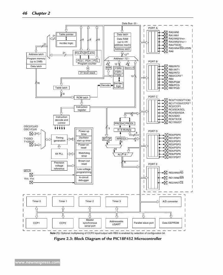
Figure 2.3: Block diagram of the PiC18F452 Microcontroller
RB7/PGDRB6/PCGRB5/PGMRB4RB3/CCP2(1)RB2/INT2RB1/INT1RB0/INT0
RD7/PSP7RD6/PSP6RD5/PSP5RD4/PSP4
RC4/SDI/SDA
RC7/RX/DTRC6/TX/CKRC5/SDO
RD3/PSP3RD2/PSP2RD1/PSP1RD0/PSP0
RA2/AN2/VREF2
RA3/AN3/VREF1
RA4/T0CKIRA5/AN4/SS/LVDIN
RC0/T1OSO/T1CKIRC1/T1OSI/CCP2(1)
RC2/CCP1RC3/SCK/SCL
RA0/AN0
PORT A
Data Bus,8.
ALU,8.
838 Multiply
PRODH PRODL
WREGBIT OP
Data latch
Data RAM(up to 4 K
address reach)
Address latch
Address,12.
12(2)
12
12
8
8
888
8
8
3
4BSR FSR0
FSR2
Decode
31-level stack
Program counter
ROM latch
Instructionregister
Instructiondecode and
control
Timinggeneration
OSC2/CLKOOSC1/CLKI
T1OSCIT1OSCO
MCLR
VDD, VSS
4X PLL
Precisionvoltage
reference
Timer 0
CCP1
Note (1): Optional multiplexing of CCP2 input/output with RB3 is enabled by selection of configuration bit.
CCP2Master
synchronousserial port
AddressableUSART
Parallel slave port Data EEPROM
A/D converterTimer 1 Timer 2 Timer 3
Power-uptimer
Power-onreset
Brown-outreset
Low-voltageprogramming
In-circuitdebugger
Watchdogtimer
Oscillatorstart-up timer
Table latch
Data latch
Address latch
Program memory(up to 2 MB)
8
16
21
8 8 8
21
21
Table pointer
inc/dec logic
PCLATU PCLATH
PCU PCH PCL
inc/declogic
FSR1
Bank 0, F
4PORT B
PORT C
PORT D
PORT E
RA1/AN1
RA6
RE0/AN5/RD
RE1/AN6/WR
RE2/AN7/CS
46 Chapter 2
www.newnespress.com

The bottom part of the diagram shows the timers/counters, capture/compare/PWM registers, USART, A/D converter, and the EEPROM data memory. PIC18F452 consists of
Four counters/timers •
Two capture/compare/PWM modules •
Two serial communication modules •
Eight 10-bit A/D converter channels •
256-byte EEPROM •
The oscillator circuit is located at the left-hand side of the diagram. This circuit consists of
PWRT •
OST •
POR •
WDT •
Brown-out reset (BOR) •
Low-voltage programming •
In-circuit debugger (ICD) •
PLL circuit •
Timing generation circuit •
The PLL is new to the PIC18F series, and it provides the option of multiplying the oscillator frequency to speed up the overall operation. The WDT can be used to force a restart of the microcontroller in the event of a program crash. The ICD is useful during program development, and it can be used to return diagnostic data, including the register values, as the microcontroller is executing a program.
The I/O ports are located at the right-hand side of the diagram. PIC18F452 consists of five parallel ports named PORTA, PORTB, PORTC, PORTD, and PORTE. Most port pins have multiple functions. For example, PORTA pins can be used as either parallel I/O or analog inputs. PORTB pins can be used as either parallel I/O or interrupt inputs.
211 Program Memory Organization
The program memory map is shown in Figure 2.4. Each PIC18F member has a 21-bit program counter and hence is capable of addressing 2 MB of memory space. User memory space on the PIC18F452 microcontroller is 00000H to 7FFFH. Accessing a nonexistent
PIC18F Microcontroller series 47
www.newnespress.com

memory location (8000H to 1FFFFFH) will cause a read of all 0s. The reset vector where the program starts after a reset is at address 0000H. Addresses 0008H and 0018H are reserved for the vectors of high-priority and low-priority interrupts, respectively, and interrupt service routines must be written to start at one of these locations.
The PIC18F microcontroller has a 31-entry stack that is used to hold the return addresses for subroutine calls and interrupt processing. The stack is not a part of the program or a data memory space. The stack is controlled by a 5-bit stack pointer, which is initialized to 00000 after a reset. During a subroutine call (or interrupt), the stack pointer is first incremented, and the memory location pointed to by the stack pointer is written using the contents of the program counter. During a return from a subroutine call (or interrupt), the memory location pointed to by the stack pointer is decremented. The projects in this
PC,20:0.
0000h
21
0018hLow-priority interrupt vector
On-chipprogram memory
7FFFh8000h U
ser
mem
ory
spac
e
1FFFFFh200000h
Read ‘0’
High-priority interrupt vector
Reset vector
Stack level 31
Stack level 1
CALL, RCALL, RETURNRETFIE, RETLW
0008h
Figure 2.4: Program Memory Map of PiC18F452
48 Chapter 2
www.newnespress.com

book are based on C language. Subroutine and interrupt call/return operations are handled automatically by the C language compiler, and thus their operation is not described here in detail.
Program memory is addressed in bytes and instructions are stored as 2 or 4 bytes in program memory. The least significant byte of an instruction word is always stored in an even address of the program memory.
An instruction cycle consists of four cycles: A fetch cycle begins with the program counter incrementing in Q1. In the execution cycle, the fetched instruction is latched into the instruc-tion register in cycle Q1. This instruction is then decoded and executed during the Q2, Q3, and Q4 cycles. A data memory location is read during Q2 and written during Q4.
212 Data Memory Organization
The data memory map of the 18F452 microcontroller is shown in Figure 2.5. The data memory address bus is 12 bits, with the capability of addressing up to 4 MB. The memory in general consists of 16 banks, each of 256 bytes. PIC18F452 has 1536 bytes of data memory (6 banks × 256 bytes each) occupying the lower end of the data memory. Bank switching is done automatically when using a high-level language compiler, and thus the user need not worry about selecting memory banks during programming.
The special function register (SFR) occupies the upper half of the top memory bank. SFR contains registers that control the operations of the microcontroller, such as the peripheral devices, timers/counters, A/D converter, interrupts, USART, and so on. Figure 2.6 shows the SFR registers of the PIC18F452 microcontroller.
213 The Configuration Registers
The PIC18F452 microcontrollers have a set of configuration registers (PIC16 series had only one configuration register). Configuration registers are programmed during the programming of the flash program memory by the programming device. These registers are shown in Table 2.2. The descriptions of these registers are given in Table 2.3. Some of the important configuration registers are described in this section in detail.
CONFIG1H
This configuration register is at address 300001H and is used to select the microcontroller clock sources. The bit patterns are shown in Figure 2.7.
CONFIG2L
This configuration register is at address 300002H and is used to select the brown-out voltage bits. The bit patterns are shown in Figure 2.8.
PIC18F Microcontroller series 49
www.newnespress.com
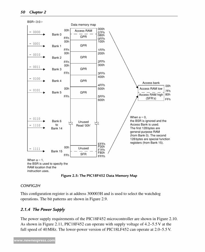
CONFIG2H
This configuration register is at address 300003H and is used to select the watchdog operations. The bit patterns are shown in Figure 2.9.
214 The Power supply
The power supply requirements of the PIC18F452 microcontroller are shown in Figure 2.10. As shown in Figure 2.11, PIC18F452 can operate with supply voltage of 4.2–5.5 V at the full speed of 40 MHz. The lower-power version of PIC18LF452 can operate at 2.0–5.5 V.
BSR,3:0.
= 0000
= 0001
= 0010
= 0011
= 0100
Bank 5
Bank 15
FFFhF80hF7FhF00hEFFh
5FFh600h
7Fh80h
FFh
When a 5 0,the BSR is ignored and theAccess Bank is used.The first 128 bytes aregeneral-purpose RAM(from Bank 0). The second128 bytes are special functionregisters (from Bank 15).
00h4FFh500h
3FFh400h
2FFh300h
1FFh200h
0FFh100h
07Fh080h
000h
UnusedRead ‘00h’
00h
00h
00h Access RAM
Data memory map
Access bank
Access RAM low
Access RAM high(SFR’s)
GPR
GPR
GPR
GPR
GPR
GPRFFh
FFh
FFh00h
FFh00h
FFh00h
FFh
Unused
SFR
When a 5 1,the BSR is used to specify theRAM location that theinstruction uses.
Bank 6to
Bank 14
Bank 4
Bank 3
Bank 2
Bank 1
Bank 0
= 0101
= 0110
= 1110
= 1111
Figure 2.5: the PiC18F452 data Memory Map
50 Chapter 2
www.newnespress.com

Figure 2.6: the PiC18F452 SFr registers
FFFh
FFEh
FFDh
FFCh
FFBh
FFAh
FF9h
FF8h
FF7h
FF6h
FF5h
FF4h
FF3h
FF2h
FF1h
FF0h
FEFh
FEEh
FEDh
FECh
FEBh
FEAh
FE9h
FE8h
FE7h
FE6h
FE5h
FE4h
FE3h
FE2h
FE1h
FE0h
(1): Unimplemented registers are read as '0'(2): This register is not available on PIC18F2X2 devices(3): This is not a physical register
FDFh
FDEh
FDDh
FDCh
FDBh
FDAh
FD9h
FD8h
FD7h
FD6h
FD5h
FD4h
FD3h
FD2h
FD1h
FD0h
FCFh
FCEh
FCDh
FCCh
FCBh
FCAh
FC9h
FC8h
FC7h
FC6h
FC5h
FC4h
FC3h
FC2h
FC1h
FC0h
FBFh
FBEh
FBDh
FBCh
FBBh
FBAh
FB9h
FB8h
FB7h
FB6h
FB5h
FB4h
FB3h
FB2h
FB1h
FB0h
FAFh
FAEh
FADh
FACh
FABh
FAAh
FA9h
FA8h
FA7h
FA6h
FA5h
FA4h
FA3h
FA2h
FA1h
FA0h
F9Fh
IPR2
EECON1
EEADR
TXSTA
RCSTA
TXREG
RCREG
SPBRG
T3CON
TMR3L
TMR3H
CCP2CON
CCPR2L
CCPR2H
CCP1CON
CCPR1L
CCPR1H
EEDATA
EECON2
PIR2
PIE2
IPR1
PIR1
PIE1
TRISE(2)
INDF2(3)
POSTINC2(3)
POSTDEC2(3)
PREINC2(3)
PLUSW2(3)
INDF0(3)
POSTINC0(3)
POSTDEC0(3)
PREINC0(3)
PLUSW0(3)
INDF1(3)
POSTINC1(3)
POSTDEC1(3)
PREINC1(3)
PLUSW1(3)
FSR1HFSR1L
BSR
FSR0H
FSR0L
WREG
FSR2H
TOSU
Address Name Address Name Address Name Address Name
TOSH
TOSL
STKPTR
PCLATU
PCLATH
PCL
TBLPTRU
TBLPTRH
TBLPTRL
TABLAT
PRODHPRODL
INTCON
INTCON2
INTCON3
FSR2L
STATUS
TMR0H
TMR0L
T0CON
OSCCON
LVDCON
WDTCON
RCON
TMR1H
TMR1L
T1CON
TMR2
PR2
T2CON
SSPBUF
SSPADD
SSPSTAT
SSPCON1
SSPCON2
ADRESH
ADRESL
ADCONO
ADCON1
TRISD(2)
LATE(2)
LATD(2)
PORTE(2)
PORTD(2)
PORTC
PORTB
PORTA
LATC
LATB
LATA
TRISC
TRISB
TRISA
F9Eh
F9Dh
F9Ch
F9Bh
F9Ah
F99h
F98h
F97h
F96h
F95h
F94h
F93h
F92h
F91h
F90h
F8Fh
F8Eh
F8Dh
F8Ch
F8Bh
F8Ah
F89h
F88h
F87h
F86h
F85h
F84h
F83h
F82h
F81h
F80h
At lower voltages, the maximum clock frequency is 4 MHz and rises to 40 MHz at 4.2 V. The RAM data retention voltage is specified as 1.5 V, and the RAM data will be lost if the power supply voltage becomes lower than this value. In practice, most microcontroller-based systems are operated with a single +5 V supply, which is derived from a suitable voltage regulator.
PIC18F Microcontroller series 51
www.newnespress.com

File
Nam
eB
it 7
Bit
6B
it 5
Bit
4B
it 3
Bit
2B
it 1
Bit
0
def
ault
/ U
npro
gram
med
V
alue
3000
01h
CO
NFI
G1H
––
OSC
SEN
––
FOSC
2FO
SC1
FOSC
0--
1- -1
11
3000
02h
CO
NFI
G2L
––
––
BO
RV1
BO
RV0
BO
REN
PWR
TEN
----
111
1
3000
03h
CO
NFI
G2H
––
––
WD
TPS2
WD
TPS1
WD
TPS0
WD
TEN
----
111
1
3000
05h
CO
NFI
G3H
––
––
––
–C
CP2
MX
----
---1
3000
06h
CO
NFI
G4L
DEB
UG
––
––
LVP
–ST
VREN
1---
-1-1
3000
08h
CO
NFI
G5L
–
––
–C
P3C
P2C
P1C
P0--
-- 1
111
3000
09h
CO
NFI
G5H
CPD
CPB
––
––
––
11--
----
3000
0Ah
CO
NFI
G6L
––
––
WR
T3W
RT2
WR
T1W
RT0
----
111
1
3000
0Bh
CO
NFI
G6H
WR
TDW
RTB
WR
TC–
––
––
111-
----
3000
0Ch
CO
NFI
G7L
––
––
EBTR
3EB
TR2
EBTR
1EB
TR0
----
111
1
3000
0Dh
CO
NFI
G7H
–EB
TRB
––
––
––
-1--
----
3FFF
FEh
DEV
ID1
DEV
2D
EV1
DEV
0R
EV4
REV
3R
EV2
REV
1R
EV0
(1)
3FFF
FFh
DEV
ID2
DEV
10D
EV9
DEV
8D
EV7
DEV
6D
EV5
DEV
4D
EV3
0000
010
0
Shad
ed c
ells
are
uni
mpl
emen
ted,
rea
d as
“0.
”
tabl
e 2.
2: P
iC18
F452
Con
figur
atio
n r
egis
ters
52 Chapter 2
www.newnespress.com

table 2.3: PiC18F452 Configuration register descriptions
Configuration Bits description
OSCSEN Clock source switching enable
FOSC2:FOSC0 Oscillator modes
BORV1:BORV0 Brown-out reset voltage
BOREN Brown-out reset enable
PWRTEN Power-up timer enable
WDTPS2:WDTPS0 Watchdog timer postscale select
WDTEN Watchdog timer enable
CCP2MX CCP2 multiplex
DEBUG Debug enable
LVP Low-voltage program enable
STVREN Stack full/underflow reset enable
CP3:CP0 Code protection
CPD EEPROM code protection
CPB Boot block code protection
WRT3:WRT0 Program memory write protection
WRTD EPROM write protection
WRTB Boot block write protection
WRTC Configuration register write protection
EBTR3:EBTR0 Table read protection
EBTRB Boot block table read protection
DEV2:DEV0 Device ID bits (001 = 18F452)
REV4:REV0 Revision ID bits
DEV10:DEV3 Device ID bits
215 The Reset
The reset action puts the microcontroller into a known state. Resetting a PIC18F microcon-troller starts the execution of the program from address 0000H of the program memory. The microcontroller can be reset during one of the following operations:
POR •
MCLR reset •
PIC18F Microcontroller series 53
www.newnespress.com

WDT reset •
BOR •
Reset instruction •
Stack full reset •
Stack underflow reset •
Figure 2.7: CONFiG1h register Bits
U-0 U-0 R/P-1 U-0 U-0 R/P-1 R/P-1 R/P-1
— — OSCSEN — — FOSC2 FOSC1 FOSC0
bit 7 bit 0
bit 7–6 Unimplemented: Read as ‘0’
bit 5 OSCSEN: Oscillator system clock switch enable bit
1 = Oscillator system clock switch option is disabled (main oscillator is source) 0 = Oscillator system clock switch option is enabled (oscillator switching is enabled)
bit 4–3 Unimplemented: Read as ‘0’
bit 2–0 FOSC2:FOSC0: Oscillator selection bits
111 = RC oscillator w/OSC2 configured as RA6 110 = HS oscillator with PLL enabled/Clock frequency = (4 × FOSC) 101 = EC oscillator w/OSC2 configured as RA6 100 = EC oscillator w/OSC2 configured as divide-by-4 clock output 011 = RC oscillator 010 = HS oscillator 001 = XT oscillator 000 = LP oscillator
Figure 2.8: CONFiG2L register Bits
U-0 U-0 U-0 U-0 R/P-1 R/P-1 R/P-1 R/P-1
— — — — BORV1 BORV0 BOREN PWRTEN
bit 7 bit 0
bit 7–4 Unimplemented: Read as '0'
bit 3–2 BORV1:BORV0: Brown-out reset voltage bits
11 = VBOR set to 2.5 V 10 = VBOR set to 2.7 V 01 = VBOR set to 4.2 V 00 = VBOR set to 4.5 V
bit 1 BOREN: Brown-out reset enable bit
1 = Brown-out reset enabled 0 = Brown-out reset disabled
bit 0 PWRTEN: Power-up timer enable bit
1 = PWRT disabled 0 = PWRT enabled
54 Chapter 2
www.newnespress.com

Figure 2.10: the PiC8F452 Power Supply Parameters
Figure 2.9: CONFiG2h register Bits
U-0 U-0 U-0 U-0 R/P-1 R/P-1 R/P-1 R/P-1
— — — — WDTPS2 WDTPS1 WDTPS0 WDTEN
bit 7 bit 0
bit 7–4 Unimplemented: Read as ‘0’
bit 3–1 WDTPS2: WDTPS0: Watchdog timer postscale select bits
111 = 1:128 110 = 1:64 101 = 1:32 100 = 1:16 011 = 1:8 010 = 1:4 001 = 1:2 000 = 1:1
bit 0 WDTEN: Watchdog timer enable bit
1 = WDT enabled 0 = WDT disabled (control is placed on the SWDTEN bit)
PIC18F Microcontroller series 55
www.newnespress.com

Generally, two types of resets are commonly used: POR and external reset using the MCLR pin.
Power-On Reset
The POR is generated automatically when power supply voltage is applied to the chip. The MCLR pin should be tied to the supply voltage directly or preferably through a 10-K resistor. Figure 2.12 shows a typical reset circuit.
For applications where the rise time of the voltage is slow, it is recommended to use a diode, a capacitor, and a series resistor, as shown in Figure 2.13.
Figure 2.12: typical reset Circuit
15 V
10 K
MCLR
PIC18FXXX
6.0 V
5.5 V
Vo
ltag
e
Frequency
PIC18LFXXX5.0 V
4.5 V
4.0 V4.2 V
3.5 V
3.0 V
2.5 V
2.0 V
4 MHz 40 MHz
Figure 2.11: Operation of PiC18LF452 at different Voltages
56 Chapter 2
www.newnespress.com

Figure 2.13: reset Circuit for Slow increasing Voltages
PIC18FXXX
MCLR
10 K100
D
C
15 V
Figure 2.14: external reset Circuit
PIC18FXXX
MCLR
10 K
Reset
15 V
In some applications, it may be required to reset the microcontroller externally by pressing a button. Figure 2.14 shows the circuit that can be used to reset the microcontroller externally. Normally, the MCLR input is at logic 1. When the Reset button is pressed, this pin goes to logic 0 and resets the microcontroller.
216 The Clock sources
The PIC18F452 microcontroller can be operated from an external crystal or a ceramic resona-tor connected to the OSC1 and OSC2 pins of the microcontroller. In addition, an external resistor and capacitor, external clock source, and in some models, internal oscillators can
PIC18F Microcontroller series 57
www.newnespress.com

be used to provide clock pulses to the microcontroller. There are eight clock sources on the PIC18F452 microcontroller, selected by the configuration register CONFIG1H. These are
Low-power crystal (LP) •
Crystal or ceramic resonator (XT) •
High-speed crystal or ceramic resonator (HS) •
High-speed crystal or ceramic resonator with PLL (HSPLL) •
External resistor/capacitor with F • OSC/4 output on OSC2 (RC)
External resistor/capacitor with I/O on OSC2 (port RA6) (RCIO) •
External clock with F • OSC/4 on OSC2 (EC)
External clock with I/O on OSC2 (port RA6) (ECIO) •
Crystal or Ceramic Resonator Operation
The first mode uses an external crystal or a ceramic resonator, which is connected to the OSC1 and OSC2 pins. For applications where the timing accuracy is important, crystal should be used. If a crystal is used, a parallel resonant crystal must be chosen because series resonant crystals do not oscillate when the system is first powered.
Figure 2.15 shows how a crystal is connected to the microcontroller. The capacitor values depend on the mode of the crystal and the selected frequency. Table 2.4 gives the recommended values. For example, for a 4-MHz crystal frequency, 15-pF capacitors can be used. Higher capacitance not only increases the oscillator stability but also increases the start-up time.
Resonators should be used in low-cost applications, where high-accuracy timing is not required. Figure 2.16 shows how a resonator is connected to the microcontroller.
Figure 2.15: Using a Crystal as the Clock input
PIC18FXXX
OSC1
C1 C2XTAL
OSC2
58 Chapter 2
www.newnespress.com

LP oscillator mode should be selected in applications in which the clock frequency is up to 200 kHz. XT mode should be selected for up to 4 MHz, and the high-speed HS mode should be selected in applications where the clock frequency is between 4 and 25 MHz.
An external clock source may also be connected to the OSC1 pin in the LP, XT, and HS modes, as shown in Figure 2.17.
External Clock Operation
An external clock source can be connected to the OSC1 input of the microcontroller in EC and ECIO modes. No oscillator start-up time is required after a POR. Figure 2.18 shows the operation with external clock in EC mode. Timing pulses with frequency FOSC/4 are available on the OSC2 pin. These pulses can be used for test purposes or to provide clock to external sources.
Figure 2.16: Using a resonator as the Clock input
PIC18FXXX
OSC1 OSC2
Resonator
table 2.4 Capacitor Values
Mode Frequency C1,C2 (pF)
LP 32 kHz 33
200 kHz 15
XT 200 kHz 22–68
1.0 MHz 15
4.0 MHz 15
HS 4.0 MHz 15
8.0 MHz 15–33
20.0 MHz 15–33
25.0 MHz 15–33
PIC18F Microcontroller series 59
www.newnespress.com

The ECIO mode is similar to the EC mode, except that the OSC2 pin can be used as a general-purpose digital I/O pin. As shown in Figure 2.19, this pin becomes bit 6 of PORTA, i.e., pin RA6.
Resistor/Capacitor Operation
There are many applications where accurate timing is not required. In such applications, we can use an external resistor and a capacitor to provide clock pulses. The clock frequency is a function of the resistor, capacitor, power supply voltage, and temperature. The clock frequency is not accurate and can vary from unit to unit due to manufacturing and component
Figure 2.17: Connecting an external Clock in LP, Xt, or hS Modes
PIC18F452
OSC1
OSC2
External clock
Figure 2.18: external Clock in eC Mode
PIC18F452
OSC1
OSC2
External clock
Fosc/4
Figure 2.19: external Clock in eCiO Mode
PIC18F452
OSC1
OSC2
External clock
RA6
60 Chapter 2
www.newnespress.com

tolerances. Table 2.5 gives the approximate clock frequency with various resistor and capacitor combinations. A close approximation of the clock frequency is 1/(4.2RC), where R should be between 3 and 10 K and C should be greater than 20 pF.
In RC mode, the oscillator frequency divided by 4 (FOSC/4) is available on pin OSC2 of the microcontroller. Figure 2.20 shows the operation at a clock frequency of approximately 2 MHz, where R = 3.9 K and C = 30 pF. In this application, the clock frequency at the output of OSC2 is 2 MHz/4 = 500 KHz.
The RCIO mode is similar to the RC mode, except that the OSC2 pin can be used as a general-purpose digital I/O pin. As shown in Figure 2.21, this pin becomes bit 6 of PORTA. i.e., pin RA6.
Crystal or Resonator with PLL
One of the problems when high-frequency crystals or resonators are used is electromagnetic interference. A PLL circuit that can be enabled to multiply the clock frequency by four is provided. Thus, for a crystal clock frequency of 10 MHz, the internal operation frequency will
table 2.5: Clock Frequency with rC
C (pF) R (K) Frequency (Mhz)
22 3.3 3.3
4.7 2.3
10 1.08
30 3.3 2.4
4.7 1.7
10 0.793
Figure 2.20: 2-Mhz Clock in rC Mode
PIC18F452
OSC1
OSC2
3.9 K
VDD
30 pF
500 kHz
PIC18F Microcontroller series 61
www.newnespress.com

be multiplied to 40 MHz. The PLL mode is enabled when the oscillator configuration bits are programmed for HS mode.
Internal Clock
Some PIC18F family members have internal clock modes (PIC18F452 has no internal clock mode). In this mode, OSC1 and OSC2 pins are available for general-purpose I/O (RA6 and RA7) or as FOSC/4 and RA7. Internal clock can be from 31 KHz to 8 MHz and is selected by registers OSCCON and OSCTUNE. Figure 2.22 shows the bits of internal clock control registers.
Clock Switching
It is possible to switch the clock from the main oscillator to a low-frequency clock source. For example, the clock can be allowed to run fast for periods of intense activity and slower when there is less activity. In the PIC18F452 microcontroller, this is controlled by bit SCS of the OSCCON register. In some of the other family members that also support internal clock, the clock switching is controlled by bits SCS0 and SCS1 of OSCCON. It is important to ensure that during clock switching, unwanted glitches do not occur in the clock signal. The 18F family contains circuitry to ensure error-free switching from one frequency to another frequency.
217 Watchdog Timer
In PIC18F family members, the WDT is a free-running on-chip RC-based oscillator, and it does not require any external components. When the WDT times out, a device reset is gener-ated. If the device is in the SLEEP mode, the WDT time-out will wake up the device and continue with normal operation.
The watchdog is enabled/disabled by bit SWDTEN of register WDTCON. Setting SWDTEN = 1 enables the WDT, and clearing this bit turns off the WDT. On the
Figure 2.21: 2-Mhz Clock in rCiO Mode
PIC18F452
OSC1
OSC2
3.9 K
VDD
30 pF
RA6
62 Chapter 2
www.newnespress.com

Figure 2.22: internal Clock Control registers
OSCCON register
IDLEN IRCF2 IRCF1 IRCF0 OSTS I0FS SCSI SCS0
IDLEN 0 Run mode enabled 1 Idle mode enabled
IRCF2:IRCF0 000 31 KHz 001 125 KHz 010 250 KHz 011 500 KHz 100 1 MHz 101 2 MHz 110 4 MHz 111 8 MHz
OSTS 0 Oscillator start-up timer running 1 Oscillator start-up timer expired
IOFS 0 Internal oscillator unstable 1 Internal oscillator stable
SCSI:SCS0 00 Primary oscillator 01 Timer 1 oscillator 10 Internal oscillator 11 Internal oscillator
OSCTUNE register
X X T5 T4 T3 T2 T1 T0
XX011111 Maximum frequency
XX000001 XX000000 Center frequency XX111111
XX100000 Minimum frequency
PIC18F452 microcontroller, an 8-bit postscaler is used to multiply the basic time-out period from 1 to 128 in powers of 2. This postscaler is controlled from configuration register CONFIG2H. The typical basic WDT time-out period is 18 ms for a postscaler value of 1.
218 Parallel I/O Ports
The parallel ports of the 18F family are very similar to those of the PIC16 series. The number of I/O ports and port pins varies depending on the PIC18F family member used, but all versions have at least PORTA and PORTB. The pins of a port are labeled as RPn, where P is
PIC18F Microcontroller series 63
www.newnespress.com

the port letter and n is the port bit number. For example, PORTA pins are labeled RA0 to RA7, PORTB pins are labeled RB0 to RB7, and so on.
When working with a port, we may want to
Set port direction •
Set an output value •
Read an input value •
Set an output value and then read back the output value •
The first three operations are the same between the PIC16 and the PIC18F series. In some applications, we may want to send a value to the port and then read back the value just sent. In the PIC16 series, there is a weakness in the port design and the value read from a port may be different from the value just written to it. This is because the reading is the actual port bit pin value, and this value could be changed by external devices connected to the port pin. In the PIC18F series, a latch register (e.g., LATA for PORTA) is introduced to the I/O ports to hold the actual value sent to a port pin. From the port, the latched value is read, which is not affected by any external devices.
In this section, we shall be looking at the general structure of I/O ports.
PORTA
In PIC18F452 microcontroller, PORTA is 7 bits wide and port pins are shared with other functions. Table 2.6 shows the PORTA pin functions.
The architecture of PORTA is shown in Figure 2.23. There are three registers associated with PORTA:
Port data register – PORTA •
Port direction register – TRISA •
Port latch register – LATA •
PORTA is the name of the port data register. The TRISA register defines the direction of PORTA pins, where a logic 1 in a bit position defines the pin as an input pin, and a 0 in a bit position defines it as an output pin. LATA is the output latch register, which shares the same data latch as PORTA. Writing to one is equivalent to writing to the other one as well. But reading from LATA activates the buffer at the top of the diagram, and the value held in PORTA/LATA data latch is transferred to the data bus, independent of the state of the actual output pin of the microcontroller.
64 Chapter 2
www.newnespress.com

Bits 0 through 3 and 5 of PORTA are also used as analog inputs. After a device reset, these pins are programmed as analog inputs, and RA4 and RA6 are configured as digital inputs. To program the analog inputs as digital I/O, the ADCON1 register (A/D register) must be programmed accordingly. Writing 7 to ADCON1 configures all PORTA pins as digital I/O.
The RA4 pin is multiplexed with the Timer 0 clock input (T0CKI). This is a Schmitt trigger input and an open drain output.
RA6 can be used as a general-purpose I/O pin, or as the OSC2 clock input, or as a clock output providing FOSC/4 clock pulses.
table 2.6: PiC18F452 POrta Pin Functions
Pin description
RA0/AN0
RA0 Digital I/O
AN0 Analog input 0
RA1/AN1
RA1 Digital I/O
AN1 Analog input 1
RA2/AN2/VREF−
RA2 Digital I/O
AN2 Analog input 2
VREF− A/D reference voltage (low) input
RA3/AN3/VREF+
RA3 Digital I/O
AN3 Analog input 3
VREF+ A/D reference voltage (high) input
RA4/T0CKI
RA4 Digital I/O
T0CKI Timer 0 external clock input
RA5/AN4/SS/LVDIN
RA5 Digital I/O
AN4 Analog input 4
SS SPI Slave Select input
RA6 Digital I/O
PIC18F Microcontroller series 65
www.newnespress.com

PORTB
In the PIC18F452 microcontroller, PORTB is an 8-bit bidirectional port shared with interrupt pins and serial device programming pins. Table 2.7 gives the PORTB bit functions.
PORTB is controlled by registers, and they are as follows:
Port data register – PORTB •
Port direction register – TRISB •
Port latch register – LATB •
The general operation of PORTB is similar to that of PORTA. Figure 2.24 shows the architecture of PORTB. Each port pin has a weak internal pull-up, which can be enabled by clearing bit RBPU
Figure 2.23: PiC18F452 POrta ra0–ra3 and ra5 Pins
RD LATADatabus
WR LATAorPORTA
WR TRISA
RD TRISA
RD PORTA
SS Input (RA5 only)
To A/D converter and LVD modules
Note (1): I/O pins have protection diodes to VDD and VSS.
TRIS latch
Data latchP
VDD
VSS
I/O pin(1)
Analoginputmode
TTLinputbuffer
N
CK
D Q
Q
CK
D Q
Q D
EN
Q
66 Chapter 2
www.newnespress.com
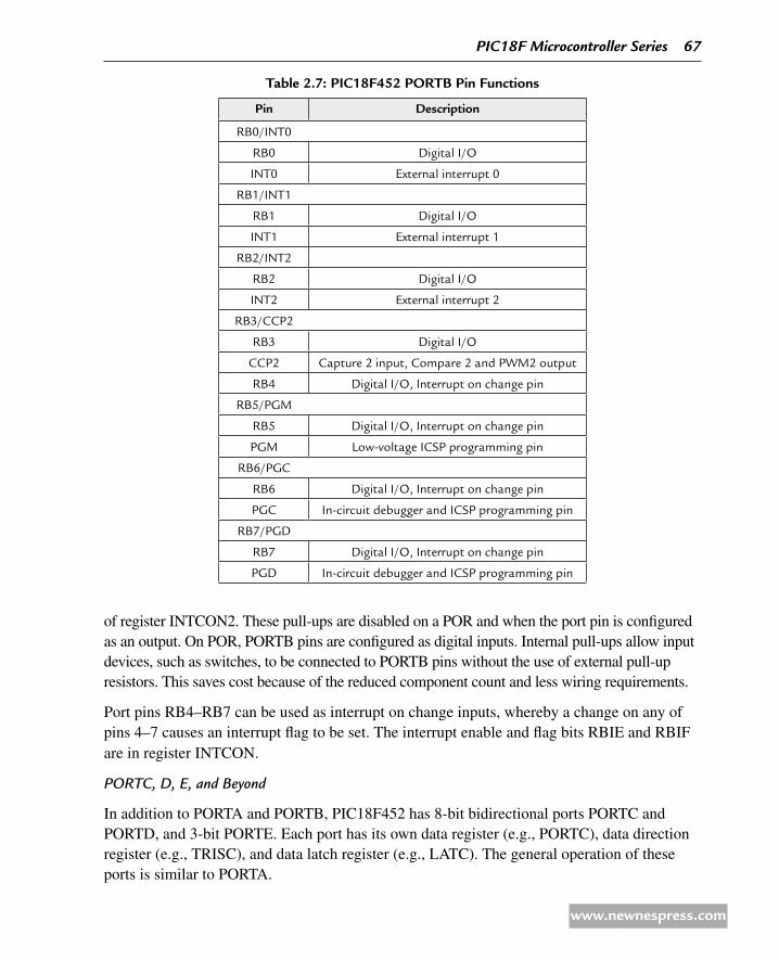
of register INTCON2. These pull-ups are disabled on a POR and when the port pin is configured as an output. On POR, PORTB pins are configured as digital inputs. Internal pull-ups allow input devices, such as switches, to be connected to PORTB pins without the use of external pull-up resistors. This saves cost because of the reduced component count and less wiring requirements.
Port pins RB4–RB7 can be used as interrupt on change inputs, whereby a change on any of pins 4–7 causes an interrupt flag to be set. The interrupt enable and flag bits RBIE and RBIF are in register INTCON.
PORTC, D, E, and Beyond
In addition to PORTA and PORTB, PIC18F452 has 8-bit bidirectional ports PORTC and PORTD, and 3-bit PORTE. Each port has its own data register (e.g., PORTC), data direction register (e.g., TRISC), and data latch register (e.g., LATC). The general operation of these ports is similar to PORTA.
table 2.7: PiC18F452 POrtB Pin Functions
Pin description
RB0/INT0
RB0 Digital I/O
INT0 External interrupt 0
RB1/INT1
RB1 Digital I/O
INT1 External interrupt 1
RB2/INT2
RB2 Digital I/O
INT2 External interrupt 2
RB3/CCP2
RB3 Digital I/O
CCP2 Capture 2 input, Compare 2 and PWM2 output
RB4 Digital I/O, Interrupt on change pin
RB5/PGM
RB5 Digital I/O, Interrupt on change pin
PGM Low-voltage ICSP programming pin
RB6/PGC
RB6 Digital I/O, Interrupt on change pin
PGC In-circuit debugger and ICSP programming pin
RB7/PGD
RB7 Digital I/O, Interrupt on change pin
PGD In-circuit debugger and ICSP programming pin
PIC18F Microcontroller series 67
www.newnespress.com

In the PIC18F452 microcontroller, PORTC is multiplexed with several peripheral functions, as shown in Table 2.8. On a POR, PORTC pins are configured as digital inputs.
In the PIC18F452 microcontroller, PORTD has Schmitt Trigger input buffers. On a POR, PORTD is configured as digital inputs. PORTD can be configured as an 8-bit PSP (i.e., microprocessor port) by setting bit 4 of the TRISE register. Table 2.9 shows functions of PORTD pins.
In the PIC18F452 microcontroller, PORTE is only 3 bits wide. As shown in Table 2.10, port pins are shared with analog inputs and parallel slave port read/write control bits. On a POR, PORTE pins are configured as analog inputs, and register ADCON1 must be programmed to change these pins to digital I/O.
STbuffer
TTLinputbuffer
RBPU(2)
Data busData latch
D
VDD
PWeakpull-up
I/O pin(1)
TRIS latch
WR LATBorPORTB
WR TRISB
RD TRISB
RD LATB
RD PORTB
Q D
Latch
Q1
Q3
EN
Q
Set RBIF
From otherRB7:RB4 pins
RB7:RB5 in serial programming mode
Note (1):(2):
I/O pins have diode protection to VDD and VSS.To enable weak pull-ups, set the appropriate TRIS bit(s)and clear the RBPU bit (INTCON2<7>).
DRD PORTB
EN
CK
Q
D
CK
Q
Figure 2.24: PiC18F452 POrtB rB4–rB7 Pins
68 Chapter 2
www.newnespress.com
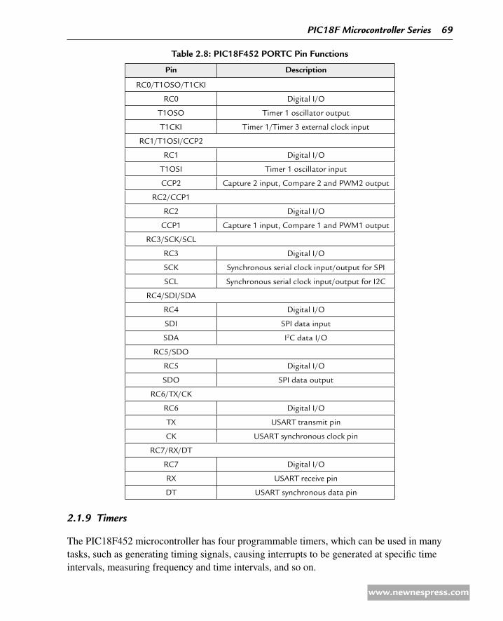
219 Timers
The PIC18F452 microcontroller has four programmable timers, which can be used in many tasks, such as generating timing signals, causing interrupts to be generated at specific time intervals, measuring frequency and time intervals, and so on.
table 2.8: PiC18F452 POrtC Pin Functions
Pin description
RC0/T1OSO/T1CKI
RC0 Digital I/O
T1OSO Timer 1 oscillator output
T1CKI Timer 1/Timer 3 external clock input
RC1/T1OSI/CCP2
RC1 Digital I/O
T1OSI Timer 1 oscillator input
CCP2 Capture 2 input, Compare 2 and PWM2 output
RC2/CCP1
RC2 Digital I/O
CCP1 Capture 1 input, Compare 1 and PWM1 output
RC3/SCK/SCL
RC3 Digital I/O
SCK Synchronous serial clock input/output for SPI
SCL Synchronous serial clock input/output for I2C
RC4/SDI/SDA
RC4 Digital I/O
SDI SPI data input
SDA I2C data I/O
RC5/SDO
RC5 Digital I/O
SDO SPI data output
RC6/TX/CK
RC6 Digital I/O
TX USART transmit pin
CK USART synchronous clock pin
RC7/RX/DT
RC7 Digital I/O
RX USART receive pin
DT USART synchronous data pin
PIC18F Microcontroller series 69
www.newnespress.com

table 2.10: PiC18F452 POrte Pin Functions
Pin description
RE0/RD/AN5
RE0 Digital I/O
RD Parallel Slave Port read control pin
AN5 Analog input 5
RE1/WR/AN6
RE1 Digital I/O
WR Parallel Slave Port write control pin
AN6 Analog input 6
RE2/CS/AN7
RE2 Digital I/O
CS Parallel Slave Port CS
AN7 Analog input 7
table 2.9: PiC18F452 POrtd Pin Functions
Pin description
RD0/PSP0
RD0 Digital I/O
PSP0 Parallel Slave Port bit 0
RD1/PSP1
RD1 Digital I/O
PSP1 Parallel Slave Port bit 1
RD2/PSP2
RD2 Digital I/O
PSP2 Parallel Slave Port bit 2
RD3/PSP3
RD3 Digital I/O
PSP3 Parallel Slave Port bit 3
RD4/PSP4
RD4 Digital I/O
PSP4 Parallel Slave Port bit 4
RD5/PSP5
RD5 Digital I/O
PSP5 Parallel Slave Port bit 5
RD6/PSP6
RD6 Digital I/O
PSP6 Parallel Slave Port bit 6
RD7/PSP7
RD7 Digital I/O
PSP7 Parallel Slave Port bit 7
70 Chapter 2
www.newnespress.com

This section introduces the timers available in the PIC18F452 microcontroller.
Timer 0
Timer 0 is similar to Timer 0 of the PIC16 series, except that it can operate either in 8-bit or in 16-bit mode. Timer 0 has the following basic features:
8-bit or 16-bit operation •
8-bit programmable prescaler •
External or internal clock source •
Interrupt generation on overflow •
Timer 0 control register is T0CON and is shown in Figure 2.25. The lower 6 bits of this register have similar functions to the PIC16 series OPTION register. The top 2 bits are used to select the 8/16-bit mode of operation and to enable/disable the timer.
Figure 2.25: timer 0 Control register, t0CON
R/W-1 R/W-1 R/W-1 R/W-1 R/W-1 R/W-1 R/W-1 R/W-1
TMR0ON T08BIT T0CS T0SE PSA TOPS2 TOPS1 TOPSO
bit 7 bit 0
bit 7 TMR0ON: Timer 0 on / off control
1 = Enables Timer 0 0 = Stops Timer 0
bit 6 T08BIT: Timer 0 8-bit/16-bit control bit
1 = Timer 0 is configured as an 8-bit timer/counter 0 = Timer 0 is configured as a 16-bit timer/counter
bit 5 T0CS: Timer 0 clock source select bit
1 = Transition on T0CKI pin 0 = Internal instruction cycle clock (CLKO)
bit 4 T0SE: Timer 0 source edge select bit
1 = Increment on high-to-low transition on T0CKI pin 0 = Increment on low-to-high transition on T0CKI pin
bit 3 PSA: Timer 0 prescaler assignment bit
1 = Timer 0 prescaler is NOT assigned. Timer 0 clock input bypasses prescaler. 0 = Timer 0 prescaler is assigned. Timer 0 clock input comes from prescaler output.
bit 2–0 T0PS2:T0PS0: Timer 0 prescaler select bits
111 = 1:256 prescale value 110 = 1:128 prescale value 101 = 1:64 prescale value 100 = 1:32 prescale value 011 = 1:16 prescale value 010 = 1:8 prescale value 001 = 1:4 prescale value 000 = 1:2 prescale value
PIC18F Microcontroller series 71
www.newnespress.com

Timer 0 can be operated either as a timer or as a counter. Timer mode is selected by clear-ing the T0CS bit, and in this mode, the clock to the timer is derived from FOSC/4. Counter mode is selected by setting the T0CS bit, and in this mode, Timer 0 is incremented on the rising or falling edge of input RA4/T0CKI. Bit T0SE of T0CON selects the edge triggering mode.
An 8-bit prescaler can be used to change the rate of the timer clock by a factor of up to 256. The prescaler is selected by bits PSA and T0PS2:T0PS0 of register T0CON.
8-Bit Mode
Figure 2.26 shows Timer 0 in 8-bit mode. The following operations are normally carried out in a timer application:
Clear T0CS to select clock F • OSC/4.
Use bits T0PS2:T0PS0 to select a suitable prescaler value. •
Clear PSA to select the prescaler. •
Load timer register TMR0L. •
Optionally enable Timer 0 interrupts. •
The timer will count up, and an interrupt will be generated when the timer value •overflows from FFH to 00H in an 8-bit mode (or from FFFFH to 0000H in 16-bit mode).
By loading a value into the TMR0 register, we can control the count until an overflow occurs. The formula given below can be used to calculate the time it will take for the timer to over-flow (or to generate an interrupt) given the oscillator period, the value loaded into the timer, and the prescaler value:
Overflow time = 4 × TOSC × Prescaler × (256 − TMR0) (2.1)
where Overflow time is in µs, TOSC is the oscillator period in µs, Prescaler is the prescaler value, and TMR0 is the value loaded into TMR0 register.
FOSC/4
RA4/T0CKI pin
T0SE
T0CS
PSA
T0PS2, T0PS1, T0PS0
(2 TCY delay)
Sync withinternalclocks
TMR0L
Set interruptflag bit TMR0IF
on overflow
Data bus
8
3
0
0
1
1Programmable
prescaler
Figure 2.26: timer 0 in an 8-bit Mode
72 Chapter 2
www.newnespress.com

For example, assume that we are using a 4-MHz crystal and the prescaler is chosen as 1:8 by setting bits PS2:PS0 to “010.” In addition, assume that the value loaded into the timer register TMR0 is decimal 100. The overflow time is then given by
4-MHz clock has a period, T = 1/f = 0.25 µs.
Using the above formula,
Overflow time = 4 × 0.25 × 8 × (256 − 100) = 1248 µs.
Thus, the timer will overflow after 1.248 ms, and a timer interrupt will be generated if the timer interrupt and global interrupts are enabled.
What we normally want is to know what value to load into the TMR0 register for a required overflow time. This can be calculated by modifying equation (2.1) as follows:
TMR0 = 256 − (Overflow time)/(4 × TOSC × Prescaler). (2.2)
For example, assume that we want an interrupt to be generated after 500 µs and the clock and the prescaler values are same as mentioned above. The value to be loaded into the TMR0 register can be calculated using (2.2) as
TMR0 = 256 − 500/(4 × 0.25 × 8) = 193.5.
The nearest number we can load into TMR0 register is 193.
16-Bit Mode
Timer 0 in 16-bit mode is shown in Figure 2.27. Here, two timer registers named TMR0L and TMR0 are used to store the 16-bit timer value. The low-byte TMR0L is directly load-able from the data bus. The high-byte TMR0 can be loaded through a buffer called TMR0H. During a read of TMR0L, the high byte of the timer (TMR0) is also loaded into TMR0H, and thus, all 16 bits of the timer value can be read. Thus, to read the 16-bit timer value, we have to first read TMR0L and then read TMR0H in a later instruction. Similarly, during a write to TMR0L, the high byte of the timer is also updated with the contents of TMR0H, allowing all 16 bits to be written to the timer. Thus, to write to the timer, the program should first write the required higher byte to TMR0H. When the lower byte is written to TMR0L, the value stored in TMR0H is automatically transferred to TMR0, thus causing all 16 bits to be written to the timer.
Timer 1
Timer 1of the PIC18F452 is a 16-bit timer controlled by register T1CON, as shown in Figure 2.28. Figure 2.29 shows the internal structure of Timer 1.
Timer 1 can be operated either as a timer or as a counter. When bit TMR1CS of register T1CON is low, clock FOSC/4 is selected for the timer. When TMR1CS is high, module
PIC18F Microcontroller series 73
www.newnespress.com
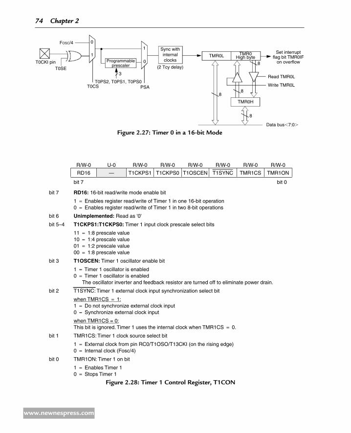
FOSC/4
T0SE
T0CS PSA
3
0
1
0
88
8
8(2 Tcy delay)
Sync withinternalclocks
TMR0L TMR0High byte
Set interruptflag bit TMR0IF
on overflow
Read TMR0L
Write TMR0L
TMR0H
Data bus,7:0.
1
T0PS2, T0PS1, T0PS0
Programmableprescaler
T0CKI pin
Figure 2.27: timer 0 in a 16-bit Mode
Figure 2.28: timer 1 Control register, t1CON
R/W-0 U-0 R/W-0 R/W-0 R/W-0 R/W-0 R/W-0 R/W-0
RD16 — T1CKPS1 T1CKPS0 T1OSCEN T1SYNC TMR1CS TMR1ON
bit 7 bit 0
bit 7 RD16: 16-bit read/write mode enable bit
1 = Enables register read/write of Timer 1 in one 16-bit operation 0 = Enables register read/write of Timer 1 in two 8-bit operations
bit 6 Unimplemented: Read as '0'
bit 5–4 T1CKPS1:T1CKPS0: Timer 1 input clock prescale select bits
11 = 1:8 prescale value 10 = 1:4 prescale value 01 = 1:2 prescale value 00 = 1:8 prescale value
bit 3 T1OSCEN: Timer 1 oscillator enable bit
1 = Timer 1 oscillator is enabled 0 = Timer 1 oscillator is enabled The oscillator inverter and feedback resistor are turned off to eliminate power drain.
bit 2 T1SYNC: Timer 1 external clock input synchronization select bit
when TMR1CS = 1: 1 = Do not synchronize external clock input 0 = Synchronize external clock input
when TMR1CS = 0: This bit is ignored. Timer 1 uses the internal clock when TMR1CS = 0.
bit 1 TMR1CS: Timer 1 clock source select bit
1 = External clock from pin RC0/T1OSO/T13CKI (on the rising edge) 0 = Internal clock (Fosc/4)
bit 0 TMR1ON: Timer 1 on bit
1 = Enables Timer 1 0 = Stops Timer 1
74 Chapter 2
www.newnespress.com

operates as a counter clocked from input T1OSI. A crystal oscillator circuit, enabled from bit T1OSCEN of T1CON, is built between pins T1OSI and T1OSO, where a crystal up to 200 KHz can be connected between these pins. This oscillator is primarily intended for a 32-KHz crystal operation in real-time clock applications. A prescaler is used in Timer 1, which can change the timing rate as a factor of 1, 2, 4, or 8.
Timer 1 can be configured so that the read/write can be performed either in a 16-bit mode or in two 8-bit modes. Bit RD16 of register T1CON controls the mode. When RD16 is low, timer's read and write are performed as two 8-bit operations. When RD16 is high, the timer's read and write operations are as in Timer 0 16-bit mode. That is, a buffer is used between the timer register and the data bus (see Figure 2.30).
If the Timer 1 interrupts are enabled, an interrupt will be generated when the timer value rolls over from FFFFH to 0000H.
Timer 2
Timer 2 is an 8-bit timer with the following features:
8-bit timer (TMR2) •
8-bit period register (PR2) •
Programmable prescaler •
Programmable postscaler •
Interrupt when TM2 matches PR2 •
TMR1IFoverflowinterruptflag bit
TMR1
TMR1H TMR1L
CLR
CCP special event trigger
TMR1ONon/off
Fosc/4internalclock
TMR1CS
T1CKPS1:T1CKPS0SLEEP input2
Synchronize
Synchronized
clock input
det
T1OSCENEnableoscillator
T1CKI/T1OSO
T1OSI
T1OSCT1SYNC
1
0
Prescaler1, 2, 4, 8
1
0
Figure 2.29: internal Structure of timer 1
PIC18F Microcontroller series 75
www.newnespress.com

Timer 2 is controlled from register T2CON, as shown in Figure 2.31. Bits T2CKPS1: T2CKPS0 set the prescaler for a scaling of 1, 4, and 16. Bits TOUTPS3:TOUTPS0 set the postscaler for a scaling of 1:1 to 1:16. The timer can be turned on or off by setting or clearing bit TMR2ON.
CCP special event trigger
TMR1ONon/off
T1SYNC
TMR1IFoverflowinterruptflag bit
Write TMR1L
Data bus<7:0>
Read TMR1L
TMR1
TMR1H
Timer 1high byte TMR1L
CLR
FOSC/4internalclock
TMR1CS
T1CKPS1:T1CKPS0
SLEEP Input2
Synchronize
Synchronized
clock input
detT1OSCENenableoscillator
T13CKI/T1OSO
T1OSI
T1OSC
Prescaler1, 2, 4, 8
0
1
1
8
8 8
8
0
Figure 2.30: timer 1 in a 16-bit Mode
Figure 2.31: timer 2 Control register, t2CON
U-0 R/W-0 R/W-0 R/W-0 R/W-0 R/W-0 R/W-0 R/W-0
— TOUTPS3 TOUTPS2 TOUTPS1 TOUTPS0 TMR2ON T2CKPS1 T2CKPS0
bit 7 bit 0
bit 7 Unimplemented: Read as '0'
bit 6–3 TOUTPS3:TOUTPS0: Timer 2 output postscale select bits
0000 = 1:1 postscale 0001 = 1:2 postscale • • • 1111 = 1:16 postscale
bit 2 TMR2ON: Timer 2 on bit
1 = Timer 2 is on 0 = Timer 2 is off
bit 1–0 T2CKPS1:T2CKPS0: Timer 2 clock prescale select bits
00 = Prescaler is 1 01 = Prescaler is 4 1x = Prescaler is 16
76 Chapter 2
www.newnespress.com

The block diagram of Timer 2 is shown in Figure 2.32. Timer 2 can be used for the PWM mode of the CCP module. The output of Timer 2 can be selected by the SSP module as a baud clock using software. Timer 2 increases from 00H until it matches PR2 and sets the interrupt flag. It then resets to 00H on the next cycle.
Timer 3
The structure and operation of Timer 3 are the same as for Timer 1, having registers TMR3H and TMR3L. This timer is controlled from register T3CON, as shown in Figure 2.33.
The block diagram of Timer 3 is shown in Figure 2.34.
2110 Capture/Compare/PWM Modules
In the PIC18F452 microcontroller, there are two Capture/Compare/PWM (CCP) modules, and they work with Timers 1, 2, and 3 to capture and compare and for PWM operations. Each module has two 8-bit registers. Module 1 registers are CCPR1L and CCPR1H, and module 2 registers are CCPR2L and CCPR2H. Together, each register pair form a 16-bit register and can be used to capture, compare, or generate waveforms with a specified duty cycle. Module 1 is controlled by register CCP1CON, and module 2 is controlled by CCP2CON. Figure 2.35 shows the bit allocations of the CCP control registers.
Capture Mode
In capture mode, the registers operate like a stopwatch, and when an event occurs, the time of the event is recorded, and the clock continues running (in a stopwatch, the watch stops when the event time is recorded).
FOSC/4
2
4
T2CKPS1:T2CKPS0
TOUTPS3:TOUTPS0
TMR2RESET
TMR2output
Sets flagbit TMR2IF
EQComparator
PR2
Postscaler1:1 to 1:16
Prescaler1:1, 1:4, 1:16
Figure 2.32: timer 2 Block diagram
PIC18F Microcontroller series 77
www.newnespress.com

Figure 2.36 shows the capture mode of operation. Here, CCP1 will be considered, but the operation of CCP2 is identical, with the register and port names change accordingly. In this mode, CCPR1H:CCPR1L captures the 16-bit value of the TMR1 or TMR3 registers when an event occurs on pin RC2/CCP1 (pin RC2/CCP1 must be configured as an input pin using TRISC). An external signal can be prescaled by 4 or 16. The event is selected by control bits CCP1M3:CCP1M0, and an event can be selected to be one of the following:
Every falling edge •
Every rising edge •
Every fourth rising edge •
Every sixteenth rising edge •
Figure 2.33: timer 3 Control register, t3CON
R/W-0 R/W-0 R/W-0 R/W-0 R/W-0 R/W-0 R/W-0 R/W-0
RD 16 T3CCP2 T3CKPS1 T3CKPS0 T3CCP1 T3SYNC TMR3CS TMR3ON
bit 7 bit 0
bit 7 RD16: 16-bit read/write mode enable bit
1 = Enables register read/write of Timer 3 in one 16-bit operation 1 = Enables register read/write of Timer 3 in two 8-bit operations
bit 6 and 3 T3CCP2:T3CCP1: Timer 3 and Timer 1 to CCPx enable bits
1x = Timer 3 is the clock source for compare/capture CCP modules 01 = Timer 3 is the clock source for compare/capture of CCP2, Timer 1 is the clock source for compare/capture of CCP1 00 = Timer 1 is the clock source for compare/capture CCP modules
bit 5–4 T3CKPS1:T3CKPS0: Timer 3 input clock prescale select bits
11 = 1:8 prescale value 10 = 1:4 prescale value 01 = 1:2 prescale value 00 = 1:1 prescale value
bit 2 T3SYNC: Timer 3 external clock input synchronization control bit (Not usable if the system clock comes from Timer 1/Timer 3) When TMR3CS = 1: 1 = Do not synchronize external clock input 0 = Synchronize external clock input When TMR3CS = 0: This bit is ignored. Timer 3 uses the internal clock when TMR3CS = 0.
bit 1 TMR3CS: Timer 3 clock source select bit 1 = External clock input from Timer 1 oscillator or T1CK1 (on the rising edge after the first falling edge) 0 = Internal clock (Fosc/4)
bit 0 TMR3ON: Timer 3 on bit 1 = Enables Timer 3 0 = Stops Timer 3
78 Chapter 2
www.newnespress.com
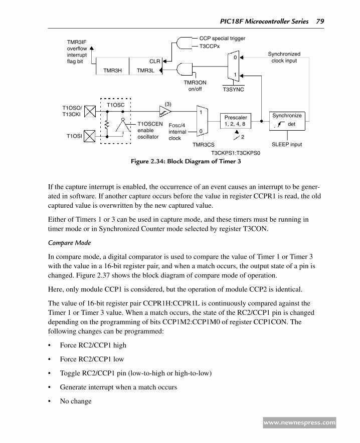
If the capture interrupt is enabled, the occurrence of an event causes an interrupt to be gener-ated in software. If another capture occurs before the value in register CCPR1 is read, the old captured value is overwritten by the new captured value.
Either of Timers 1 or 3 can be used in capture mode, and these timers must be running in timer mode or in Synchronized Counter mode selected by register T3CON.
Compare Mode
In compare mode, a digital comparator is used to compare the value of Timer 1 or Timer 3 with the value in a 16-bit register pair, and when a match occurs, the output state of a pin is changed. Figure 2.37 shows the block diagram of compare mode of operation.
Here, only module CCP1 is considered, but the operation of module CCP2 is identical.
The value of 16-bit register pair CCPR1H:CCPR1L is continuously compared against the Timer 1 or Timer 3 value. When a match occurs, the state of the RC2/CCP1 pin is changed depending on the programming of bits CCP1M2:CCP1M0 of register CCP1CON. The following changes can be programmed:
Force RC2/CCP1 high •
Force RC2/CCP1 low •
Toggle RC2/CCP1 pin (low-to-high or high-to-low) •
Generate interrupt when a match occurs •
No change •
CCP special trigger
T3CCPx
TMR3ONon/off T3SYNC
TMR3IFoverflowinterruptflag bit
TMR3H TMR3L
(3)
CLR
FOSC/4internalclock
TMR3CS
T3CKPS1:T3CKPS0
SLEEP input2
Synchronize
Synchronizedclock input
detT1OSCENenableoscillator
T1OSO/T13CKI
T1OSI
T1OSC
Prescaler1, 2, 4, 8
0
1
1
0
Figure 2.34: Block diagram of timer 3
PIC18F Microcontroller series 79
www.newnespress.com

Timer 1 or Timer 3 must be running in Timer mode or in Synchronized Counter mode selected by register T3CON.
2111 Pulse Width Modulation Module
The Pulse Width Modulation (PWM) mode produces a PWM output at 10-bit resolution. A PWM output is basically a square waveform with a specified period and duty cycle. Figure 2.38 shows a typical PWM waveform.
Figure 2.39 shows the PWM module block diagram. The module is controlled by Timer 2. The PWM period is given by
PWM period = (PR2 + 1) × TMR2PS × 4 × TOSC (2.3)
Figure 2.35: CCPxCON register Bit allocations
U-0 U-0 R/W-0 R/W-0 R/W-0 R/W-0 R/W-0 R/W-0
— — DC × B1 DC × B0 CCP × M3 CCP × M2 CCP × M1 CCP × M0
bit 7 bit 0
bit 7–6 Unimplemented: Read as ‘0’
bit 5–4 DC × B1:DC×B0: PWM duty cycle bit 1 and bit 0
Capture mode:
Unused
Compare mode:
Unused
PWM mode:
These bits are the two LSbs (bit 1 and bit 0) of the 10-bit PWM duty cycle. The upper eight bits (DC × 9:DC × 2) of the duty cycle are found in CCPRxL.
bit 3–0 CCP × M3: CCP × M0: CCPx mode select bits
0000 = Capture/compare/PWM disabled (resets CCPx module) 0001 = Reserved 0010 = Compare mode, toggle output on match (CCPxIF bit is set) 0011 = Reserved 0100 = Capture mode, every falling edge 0101 = Capture mode, every rising edge 0110 = Capture mode, every 4th rising edge 0111 = Capture mode, every 16th rising edge 1000 = Compare mode,
Initialize CCP pin Low, on compare match force CCP pin High (CCPIF bit is set) 1001 = Compare mode,
Initialize CCP pin High, on compare match force CCP pin Low (CCPIF bit is set) 1010 = Compare mode,
Generate software interrupt on compare match (CCPIF bit is set, CCP pin is unaffected)
1011 = Compare mode, Trigger special event (CCPIF bit is set)
11xx = PWM mode
80 Chapter 2
www.newnespress.com

Set flag bit CCP1IF
CCP1 pin
Prescaler÷ 1, 4, 16
andEdge Detect
Q’sCCP1CON<3:0>
andEdge Detect
Q’sCCP2CON<3:0>
Prescaler÷ 1, 4, 16
CCP2 pin
Set flag bit CCP2IF
T3CCP2
T3CCP2
T3CCP1T3CCP2
T3CCP2T3CCP1
TMR3H TMR3L
TMR1H TMR1L
CCPR1H
TMR3
Enable
TMR1
Enable
CCPR1L
TMR3H TMR3L
TMR1H TMR1L
CCPR2H
TMR3
Enable
TMR1
Enable
CCPR2L
Figure 2.36: Capture Mode of Operation
Special event trigger
CCP2CON<3:0>Mode select
Outputlogic
TRISC<1>Output enable
RC1/CCP2 pin
Set flag bit CCP2IF
Set flag bit CCP1IF
Match
Special event trigger
Q S
R
Q S
R
CCP1CON<3:0>Mode select
Outputlogic
TRISC<2>Output enable
RC2/CCP1 pin Match
Comparator
Comparator
0 1
1
CCPR2H CCPR2L
CCPR1H CCPR1L
T3CCP1
TMR1H TMR1L TMR3H TMR3L
T3CCP2
T3CCP2
0
Figure 2.37: Compare Mode of Operation
PIC18F Microcontroller series 81
www.newnespress.com

or
PR2 = PWM period
TMR2PS × 4 × TOSC − 1, (2.4)
where PR2 is the value loaded into Timer 2 register, TMR2PS is the Timer 2 prescaler value, TOSC is the clock oscillator period (seconds).
The PWM frequency is defined as 1/(PWM period).
The resolution of the PWM duty cycle is 10 bits. The PWM duty cycle is selected by writing the eight most significant bits into the CCPR1L register and the two least significant bits into bits 4 and 5 of CCP1CON register. The duty cycle (in seconds) is given by
PWM duty cycle = (CCPR1L:CCP1CON < 5: 4 >) × TMR2PS × TOSC (2.5)
or
CCPR1L:CCP1CON < 5:4 > = PWM duty cycle
TMR2PS × TOSC
(2.6)
Figure 2.38: typical PWM Waveform
Period
Duty cycle
Figure 2.39: PWM Module Block diagram
Duty cycle registers
CCPR1L
CCPR1H (Slave)
Comparator
Comparator
TMR2
PR2
R
S
TRISC<2>
RC2/CCP1
Q
Clear timer,CCP1 pin andlatch DC
CCP1CON<5:4>
82 Chapter 2
www.newnespress.com

The steps to configure the PWM are as follows:
Specify the required period and duty cycle. •
Choose a value for Timer 2 prescaler (TMR2PS). •
Calculate the value to be written into PR2 register using equation (2.2). •
Calculate the value to be loaded into CCPR1L and CCP1CON registers using •equation (2.6).
Clear the bit 2 of TRISC to make CCP1 pin an output pin. •
Configure the CCP1 module for PWM operation using register CCP1CON. •
An example is given below to show how the PWM can be set up.
example 2.1
It is required to generate PWM pulses from pin CCP1 of a PIC18F452 microcontroller. The required pulse period is 44 µs, and the required duty cycle is 50%. Assuming that the microcontroller operates with a 4-MHz crystal, calculate the values to be loaded into various registers.
solution
Using a 4-MHz crystal, calculate TOSC = 1/4 = 0.25 × 10⁻⁶.
The required PWM duty cycle is 44/2 = 22 µs.
From equation (2.4), assuming a timer prescaler factor of 4, we have
PR2 = PWM period
TMR2PS × 4 × TOSC − 1
or
PR2 = 44 × 10−6 4 × 4 × 0.25
× 10−6 − 1 = 10, i.e., 0AH
and from equation (2.6)
CCPR1L:CCP1CON < 5:4 > = PWM duty cycle
TMR2PS × TOSC
or
CCPR1L:CCP1CON < 5:4 > = 22 × 10−6
4 × 0.25 × 10−6 = 22.
But the equivalent of number 22 in 10-bit binary is 00 00010110.
PIC18F Microcontroller series 83
www.newnespress.com

Therefore, the value to be loaded into bits 4 and 5 of CCP1CON is 00. Bits 2 and 3 of CCP1CON must be set to high for PWM operation. Therefore, CCP1CON must be set to bit pattern (“X” is don’t care): XX001100
Considering the don’t care entries as 0, we can set CCP1CON to hexadecimal 0CH.
The value to be loaded into CCPR1L is 00010110, i.e., hexadecimal number 16H.
The required steps are summarized below.
Load Timer 2 with prescaler of 4, i.e., load T2CON with 00000101, which is 05H. •
Load 0AH into PR2. •
Load 16H into CCPR1L. •
Load 0 into TRISC (make CCP1 pin output). •
Load 0CH into CCP1CON. •
One period of the generated PWM waveform is shown in Figure 2.40.
2112 Analog-to-Digital Converter Module
An A/D converter is another important peripheral component of a microcontroller. The A/D con-verts an analog input voltage into a digital number so that it can be processed by a microcontroller or any other digital system. There are many A/D chips available in the market, and an embedded designer should understand the characteristics of such chips so that the chips can be used efficiently.
A/D converters can be classified into two types as far as the input and output voltage are concerned. These are unipolar and bipolar. Unipolar A/D converters accept unipolar input voltages in the range 0 to +V, and bipolar A/D converters accept bipolar input voltages in the range ±V. Bipolar converters are frequently used in signal processing applications, where the signals by nature are bipolar. Unipolar converters are usually cheaper, and they are used in many control and instrumentation applications.
Figure 2.41 shows the typical steps involved in reading and converting an analog signal into digital form. This is also known as the process of signal conditioning. Signals received from sensors usually need to be processed before being fed to an A/D converter. The processing
Figure 2.40: Generated PWM Waveform
44 ms
22 ms 22 ms
84 Chapter 2
www.newnespress.com

usually consists of scaling the signal to the correct value. Unwanted signal components are then removed by filtering the signal using classical filters (e.g., low-pass filter). The final processing stage before feeding the signal to an A/D converter is to pass the signal through a sample-and-hold device. This is particularly important for fast real-time signals whose value may be changing between the sampling instants. A sample-and-hold device ensures that the signal stays at a constant value during the actual conversion process. In many applications, it is usually required to have more than one A/D, and this is normally done by using an analog multiplexer at the input of the A/D. The multiplexer selects only one signal at any time and presents this signal to the actual A/D converter. An A/D converter usually has a single analog input and a digital parallel output. The conversion process is as follows:
Apply the processed signal to the A/D input. •
Start the conversion. •
Wait until conversion is complete. •
Read the converted digital data. •
The A/D conversion starts by triggering the converter. Depending on the speed of the converter, the actual conversion process can take several microseconds. At the end of the conversion, the converter either raises a flag or generates an interrupt to indicate that the conversion is complete. The converted parallel output data can then be read by the digital device connected to the A/D converter.
Most PIC18F family members contain a 10-bit A/D converter. If the voltage reference is chosen to be +5 V, the voltage step value is
( 5 V 1023 ) = 0.00489 V or 4.89 mV.
Therefore, for example, if the input voltage is 1.0 V, the converter will generate a digital output of 1.0/0.00489 = 205 decimal. Similarly, if the input voltage is 3.0 V, the converter will generate 3.0/0.00489 = 613.
Figure 2.41: Signal Conditioning and a/d Conversion Process
Analogsignal
Scaling FilterSample
&hold
Mux.A/D
converter
PIC18F Microcontroller series 85
www.newnespress.com

The A/D converter used by the PIC18F452 microcontroller has eight channels, called AN0–AN7, and these channels are shared by the PORTA and PORTE pins. Figure 2.42 shows the block diagram of the A/D converter.
The A/D converter has four registers. Registers ADRESH and ADRESL store the higher and lower results of the conversion, respectively. Register ADCON0, shown in Figure 2.43, controls the operation of the A/D module, such as selecting the conversion clock (together with register ADCON1), selecting an input channel, starting a conversion, and powering-up and shutting-down the A/D converter.
The ADCON1 register (see Figure 2.44) is used for selecting the conversion format, configur-ing the A/D channels for analog input, selecting the reference voltage, and selecting the conversion clock (together with ADCON0).
The A/D conversion starts by setting the GO/DONE bit of ADCON0. When the conversion is complete, the 2 bits of the converted data are written into register ADRESH, and the remaining 8 bits are written into register ADRESL. At the same time, the GO/DONE bit is cleared to indicate the end of conversion. If required, interrupts can be enabled so that a software interrupt is generated when the conversion is complete.
Figure 2.42 Block diagram of the PiC18F452 a/d Converter
10-bitconverter
A/D
Referencevoltage
VREF1
VREF2
VSS
VDD
PCFG<3:0>
CHS<2:0>
111
110
101
100
011
010
001
000AN0
AN1
AN2
AN3
AN4
AN5
AN6
AN7
(Input voltage)
VAIN
86 Chapter 2
www.newnespress.com
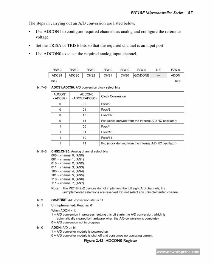
The steps in carrying out an A/D conversion are listed below.
Use ADCON1 to configure required channels as analog and configure the reference •voltage.
Set the TRISA or TRISE bits so that the required channel is an input port. •
Use ADCON0 to select the required analog input channel. •
Figure 2.43: adCON0 register
R/W-0 R/W-0 R/W-0 R/W-0 R/W-0 R/W-0 U-0 R/W-0
ADCS1 ADCS0 CHS2 CHS1 CHS0 GO/DONE — ADON
bit 7 bit 0
bit 7–6 ADCS1:ADCS0: A/D conversion clock select bits
ADCON1 <ADCS2>
ADCON0<ADCS1:ADCS0>
Clock Conversion
0 00 Fosc/2
0 01 Fosc/8
0 10 Fosc/32
0 11 Frc (clock derived from the internal A/D RC oscillator)
1 00 Fosc/4
1 01 Fosc/16
1 10 Fosc/64
1 11 Frc (clock derived from the internal A/D RC oscillator)
bit 5–3 CHS2:CHS0: Analog channel select bits 000 = channel 0, (AN0) 001 = channel 1, (AN1) 010 = channel 2, (AN2) 011 = channel 3, (AN3) 100 = channel 4, (AN4) 101 = channel 5, (AN5) 110 = channel 6, (AN6) 111 = channel 7, (AN7)
Note: The PIC18F2×2 devices do not implement the full eight A/D channels; the unimplemented selections are reserved. Do not select any unimplemented channel.
bit 2 GO/DONE: A/D conversion status bit
bit 1 Unimplemented: Read as '0'
When ADON = 1: 1 = A/D conversion in progress (setting this bit starts the A/D conversion, which is
automatically cleared by hardware when the A/D conversion is complete) 0 = A/D conversion not in progress
bit 0 ADON: A/D on bit 1 = A/D converter module is powered up 0 = A/D converter module is shut off and consumes no operating current
PIC18F Microcontroller series 87
www.newnespress.com

Figure 2.44: adCON1 register
R/W-0 R/W-0 U-0 U-0 R/W-0 R/W-0 R/W-0 R/W-0
ADFM ADCS2 — — PCFG3 PCFG2 PCFG1 PCFG0
bit 7 bit 0
bit 7 ADFM: A/D result format select bit 1 = Right justified. Six (6) most significant bits of ADRESH are read as '0'. 0 = Left justified. Six (6) least significant bits of ADRESL are read as '0'.
bit 6 ADCS2: A/D conversion clock select bit
ADCON1 <ADCS2>
ADCON0 <ADCS1:ADCS0>
Clock Conversion
0 00 Fosc/2
0 01 Fosc/8
0 10 Fosc/32
0 11 Frc (clock derived from the internal A/D RC oscillator)
1 00 Fosc/4
1 01 Fosc/16
1 10 Fosc/64
1 11 Frc (clock derived from the internal A/D RC oscillator)
bit 5–4 Unimplemented: Read as '0'
bit 3–0 PCFG3:PCFG0: A/D port configuration control bits
PCFG <3:0>
AN7 AN6 AN5 AN4 AN3 AN2 AN1 AN0 Vref+ Vref- C/R
0000 A A A A A A A A VDD Vss 8/0
0001 A A A A VREF+ A A A AN3 Vss 7/1
0010 D D D A A A A A VDD Vss 5/0
0011 D D D A VREF+ A A A AN3 Vss 4/1
0100 D D D D A D A A VDD Vss 3/0
0101 D D D D VREF+ D A A AN3 Vss 2/1
011x D D D D D D D D — — 0/0
1000 A A A A VREF+ VREF− A A AN3 AN2 6/2
1001 D D A A A A A A VDD Vss 6/0
1010 D D A A VREF+ A A A AN3 Vss 5/1
1011 D D A A VREF+ VREF− A A AN3 AN2 4/2
1100 D D D A VREF+ VREF− A A AN3 AN2 3/2
1101 D D D D VREF+ VREF− A A AN3 AN2 2/2
1110 D D D D D D D A VDD Vss 1/0
1111 D D D D VREF+ VREF− D A AN3 AN2 1/2
A = Analog input D = Digital I/O
88 Chapter 2
www.newnespress.com
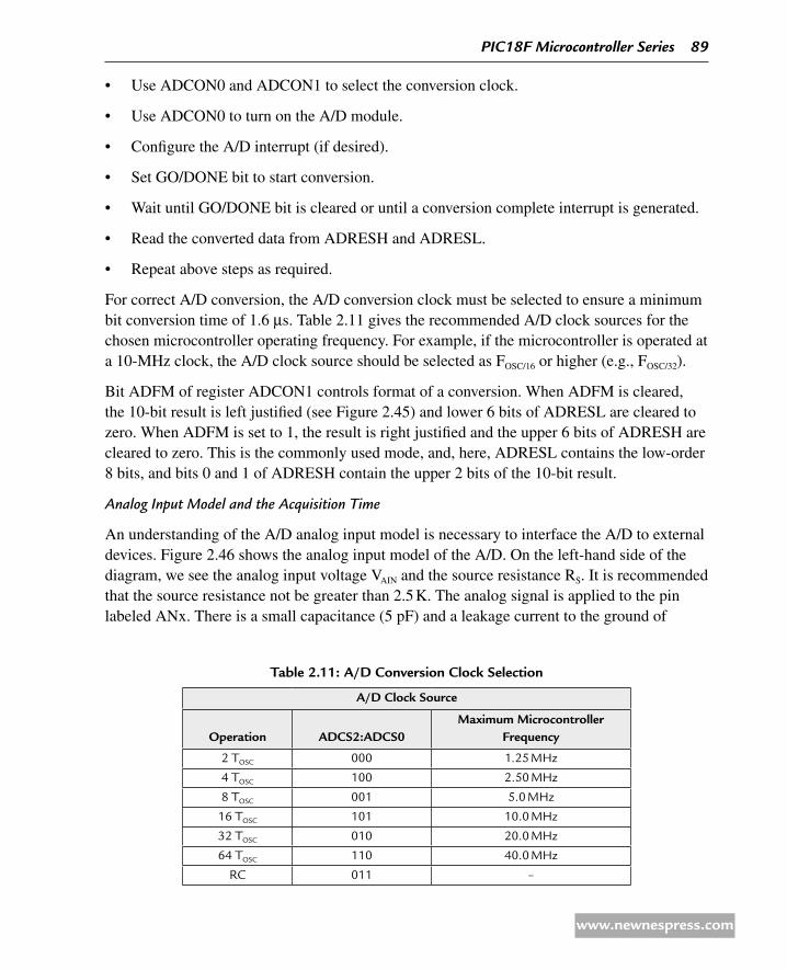
Use ADCON0 and ADCON1 to select the conversion clock. •
Use ADCON0 to turn on the A/D module. •
Configure the A/D interrupt (if desired). •
Set GO/DONE bit to start conversion. •
Wait until GO/DONE bit is cleared or until a conversion complete interrupt is generated. •
Read the converted data from ADRESH and ADRESL. •
Repeat above steps as required. •
For correct A/D conversion, the A/D conversion clock must be selected to ensure a minimum bit conversion time of 1.6 µs. Table 2.11 gives the recommended A/D clock sources for the chosen microcontroller operating frequency. For example, if the microcontroller is operated at a 10-MHz clock, the A/D clock source should be selected as FOSC/16 or higher (e.g., FOSC/32).
Bit ADFM of register ADCON1 controls format of a conversion. When ADFM is cleared, the 10-bit result is left justified (see Figure 2.45) and lower 6 bits of ADRESL are cleared to zero. When ADFM is set to 1, the result is right justified and the upper 6 bits of ADRESH are cleared to zero. This is the commonly used mode, and, here, ADRESL contains the low-order 8 bits, and bits 0 and 1 of ADRESH contain the upper 2 bits of the 10-bit result.
Analog Input Model and the Acquisition Time
An understanding of the A/D analog input model is necessary to interface the A/D to external devices. Figure 2.46 shows the analog input model of the A/D. On the left-hand side of the diagram, we see the analog input voltage VAIN and the source resistance RS. It is recommended that the source resistance not be greater than 2.5 K. The analog signal is applied to the pin labeled ANx. There is a small capacitance (5 pF) and a leakage current to the ground of
table 2.11: a/d Conversion Clock Selection
a/d Clock Source
Operation adCS2:adCS0Maximum Microcontroller
Frequency
2 TOSC 000 1.25 MHz
4 TOSC 100 2.50 MHz
8 TOSC 001 5.0 MHz
16 TOSC 101 10.0 MHz
32 TOSC 010 20.0 MHz
64 TOSC 110 40.0 MHz
RC 011 –
PIC18F Microcontroller series 89
www.newnespress.com

approximately 500 nA. RIC is the interconnect resistance, which has a value of less than 1 K. The sampling process is shown with switch SS, having a resistance RSS whose value depends on the voltage as shown in the small graph in the bottom of Figure 2.46. The value of RSS is approximately 7 K at 5 V of supply voltage.
Figure 2.45: Formatting the a/d Conversion result
10-bit result
10-bit result
ADFM 5 1 ADFM 5 0
7 2 1 0 7 0 7 0 7 6 5 0
0000 00 0000 00
ADRESH ADRESL
10-bit result
ADRESH ADRESL
Right justified Left justified
Figure 2.46: analog input Model of the a/d Converter
Rs
CPIN
VDD
VT 5 0.6 V
VT 5 0.6 V I LEAKAGE
6 500 nACHOLD 5 120 pF
Samplingswitch
RIC # 1KANx
5 pF
SS RSS
VSS
VDD
VAIN
Legend: CPIN
VT
I LEAKAGE
5 threshold voltage5 leakage current at the pin due to various junctions
RIC 5 interconnect resistanceSS 5 sampling switchCHOLD 5 sample/hold capacitance (from DAC)
5 input capacitance6 V5 V4 V3 V2 V
Sampling switch (KV)5 6 7 8 9 10 11
90 Chapter 2
www.newnespress.com
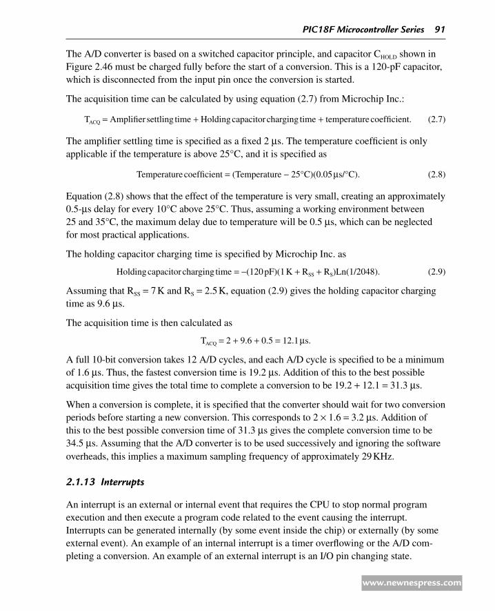
The A/D converter is based on a switched capacitor principle, and capacitor CHOLD shown in Figure 2.46 must be charged fully before the start of a conversion. This is a 120-pF capacitor, which is disconnected from the input pin once the conversion is started.
The acquisition time can be calculated by using equation (2.7) from Microchip Inc.:
TACQ = Amplifier settling time + Holding capacitor charging time + temperature coefficient. (2.7)
The amplifier settling time is specified as a fixed 2 µs. The temperature coefficient is only applicable if the temperature is above 25°C, and it is specified as
Temperature coefficient = (Temperature − 25°C)(0.05 µs/°C). (2.8)
Equation (2.8) shows that the effect of the temperature is very small, creating an approximately 0.5-µs delay for every 10°C above 25°C. Thus, assuming a working environment between 25 and 35°C, the maximum delay due to temperature will be 0.5 µs, which can be neglected for most practical applications.
The holding capacitor charging time is specified by Microchip Inc. as
Holding capacitor charging time = −(120 pF)(1 K + RSS + RS)Ln(1/2048). (2.9)
Assuming that RSS = 7 K and RS = 2.5 K, equation (2.9) gives the holding capacitor charging time as 9.6 µs.
The acquisition time is then calculated as
TACQ = 2 + 9.6 + 0.5 = 12.1 µs.
A full 10-bit conversion takes 12 A/D cycles, and each A/D cycle is specified to be a minimum of 1.6 µs. Thus, the fastest conversion time is 19.2 µs. Addition of this to the best possible acquisition time gives the total time to complete a conversion to be 19.2 + 12.1 = 31.3 µs.
When a conversion is complete, it is specified that the converter should wait for two conversion periods before starting a new conversion. This corresponds to 2 × 1.6 = 3.2 µs. Addition of this to the best possible conversion time of 31.3 µs gives the complete conversion time to be 34.5 µs. Assuming that the A/D converter is to be used successively and ignoring the software overheads, this implies a maximum sampling frequency of approximately 29 KHz.
2113 Interrupts
An interrupt is an external or internal event that requires the CPU to stop normal program execution and then execute a program code related to the event causing the interrupt. Interrupts can be generated internally (by some event inside the chip) or externally (by some external event). An example of an internal interrupt is a timer overflowing or the A/D com-pleting a conversion. An example of an external interrupt is an I/O pin changing state.
PIC18F Microcontroller series 91
www.newnespress.com
Interrupts can be useful in many applications and some are as follows:
• Time critical applications: Applications that require immediate attention of the CPU can use interrupts. For example, emergency events, such as power failure or fire in a plant, may require the CPU to shut down the system immediately in an orderly manner. Using an external interrupt in such applications will force the CPU to stop whatever it is doing and take immediate action.
• Performing routine tasks: There are many applications that require the CPU to perform routine work. For example, it may be required to check the state of a peripheral device exactly at every millisecond. By creating a timer interrupt with the required scheduling time, the CPU can be diverted from normal program execution, and the state of the peripheral can be checked exactly at required times.
• Task switching in multitasking applications: In multitasking applications, each task may be given a finite time to execute its code. Interrupt mechanisms can be used to stop a task if more time is consumed than allocated for it.
• To service peripheral devices quickly: In some applications, we may have to wait for the completion of a task, such as the completion of the A/D conversion. This can be done by continuously checking the completion flag of the A/D converter. A more elegant solution would be to enable the A/D completion interrupt so that the CPU is forced to read the converted data as soon as it becomes available.
The PIC18F452 microcontroller has core and peripheral interrupt sources. The core interrupt sources are as follows:
External edge-triggered interrupt on INT0, INT1, and INT2 pins •
PORTB pins change interrupts (any one of RB4–RB7 pins changing state) •
Timer 0 overflow interrupt •
The PIC18F452 peripheral interrupt sources are as follows:
PSP read/write interrupt •
A/D conversion complete interrupt •
USART receive interrupt •
USART transmit interrupt •
Synchronous serial port interrupt •
CCP1 interrupt •
TMR1 overflow interrupt •
92 Chapter 2
www.newnespress.com

TMR2 overflow interrupt •
Comparator interrupt •
EEPROM/FLASH write interrupt •
Bus collision interrupt •
Low-voltage detect interrupt •
Timer 3 overflow interrupt •
CCP2 interrupt •
Interrupts in the PIC18F family can be divided into two groups: a high-priority group and a low-priority group. Applications that require more attention can be placed in the high-priority group. A high-priority interrupt can stop a low-priority interrupt in progress and gain access to the CPU. High-priority interrupts cannot be stopped by low-priority interrupts. If the application does not need to set priorities for interrupts, the user can choose to disable the priority scheme so that all interrupts are at the same priority level. High-priority interrupts are vectored to address 00008H and low-priority ones to address 000018H of the program memory. Normally, a user program code (interrupt service routine [ISR]) should be at the interrupt vector address to service the interrupting device.
In the PIC18F452 microcontroller, there are 10 registers that control interrupt operations. These registers are as follows:
RCON •
INTCON •
INTCON2 •
INTCON3 •
PIR1, PIR2 •
PIE1, PIE2 •
IPR1, IPR2 •
Each interrupt source (except INT0) has 3 bits to control its operation. These bits are
A flag bit to indicate whether an interrupt has occurred. This bit has a name ending in IF. •
An interrupt enable bit to enable or disable the interrupt source. This bit has a name •ending in IE.
A priority bit to select high or low priority. This bit has a name ending in IP. •
PIC18F Microcontroller series 93
www.newnespress.com

RCON Register
The top bit of the RCON register, called IPEN, is used to enable the interrupt priority scheme. When IPEN = 0, interrupt priority levels are disabled, and the microcontroller interrupt structure is similar to the PIC16 series. When IPEN = 1, interrupt priority levels are enabled. Figure 2.47 shows the bits of register RCON.
Enabling/Disabling Interrupts – No Priority Structure
When the IPEN bit is cleared, the priority feature is disabled. All interrupts branch to address 00008H of the program memory. In this mode, bit PEIE of register INTCON enables/disables all peripheral interrupt sources. Similarly, bit GIE of INTCON enables/disables all interrupt sources. Figure 2.48 shows the bits of register INTCON.
For an interrupt to be accepted by the CPU, the following conditions must be satisfied:
Interrupt enable bit of the interrupt source must be enabled. For example, if the interrupt •source is an external interrupt pin INT0, then bit INT0IE of register INTCON must be set to 1.
The interrupt flag of the interrupt source must be cleared. For example, if the interrupt •source is an external interrupt pin INT0, then bit INT0IF of register INTCON must be cleared to 0.
Peripheral interrupt enable/disable bit PEIE of INTCON must be set to 1 if the interrupt •source is a peripheral.
Global interrupt enable/disable bit GIE of INTCON must be set to 1. •
Figure 2.47: rCON register Bits
R/W-0 U-0 U-0 R/W-1 R-1 R-1 R/W-0 R/W-0
IPEN — — RI TO PD POR BOR
bit 7 bit 0
bit 7 IPEN: Interrupt priority enable bit 1 = Enable priority levels on interrupts 0 = Disable priority levels on interrupts (16CXXX compatibility mode)
bit 6–5 Unimplemented: Read as '0'
bit 4 RI: Reset instruction flag bit
bit 3 TO: Watchdog time-out flag bit
bit 2 PD: Power-down detection flag bit
bit 1 POR: Power-on reset status bit
bit 0 BOR: Brown-out reset operation
94 Chapter 2
www.newnespress.com

For an external interrupt source, we normally have to define whether the interrupt should occur on the low-to-high or high-to-low transition of the interrupt source. For example, for INT0 interrupts, this is done by setting/clearing bit INTEDG0 of register INTCON2.
When an interrupt occurs, the CPU stops its normal flow of execution, pushes the return address onto the stack, and jumps to address 00008H in the program memory,
Figure 2.48: iNtCON register Bits
R/W-0 R/W-0 R/W-0 R/W-0 R/W-0 R/W-0 R/W-0 R/W-x
GIE/GIEH PEIE/GIEL TMR0IE INT0IE RBIE TMR0IF INT0IF RBIF
bit 7 bit 0
bit 7 GIE/GIEH: Global interrupt enable bit
When IPEN = 0: 1 = Enables all unmasked interrupts 0 = Disables all interrupts
When IPEN = 1: 1 = Enables all high-priority interrupts 0 = Disables all interrupts
bit 6 PEIE/GIEL: Peripheral interrupt enable bit
When IPEN = 0: 1 = Enables all unmasked peripheral interrupts 0 = Disables all peripheral interrupts
When IPEN = 1: 1 = Enables all low-priority peripheral interrupts 0 = Disables all low-priority peripheral interrupts
bit 5 TMR0IE: TMR0 overflow interrupt enable bit 1 = Enables the TMR0 overflow interrupt 0 = Disables the TMR0 overflow interrupt
bit 4 INT0IE: INT0 external interrupt enable bit 1 = Enables the INT0 external interrupt 1 = Disables the INT0 external interrupt
bit 3 RBIE: RB port change interrupt enable bit 1 = Enables the RB port change interrupt 0 = Disables the RB port change interrupt
bit 2 TMR0IF: TMR0 overflow interrupt flag bit 1 = TMR0 register has overflowed (must be cleared in software) 0 = TMR0 register did not overflow
bit 1 INT0IF: INT0 external interrupt flag bit 1 = The INT0 external interrupt occurred (must be cleared in software) 0 = The INT0 external interrupt did not occur
bit 0 RBIF: RB port change interrupt flag bit 1 = At least one of the RB7:RB4 pins changed state (must be cleared in software) 0 = None of the RB7:RB4 pins has changed state
Note: A mismatch condition will continue to set this bit. Reading PORTB will end the mismatch condition and allow the bit to be cleared.
PIC18F Microcontroller series 95
www.newnespress.com
where the user interrupt service routine program resides. Once in the interrupt service routine, the global interrupt enable bit (GIE) is cleared to disable further interrupts. When multiple interrupt sources are enabled, the source of the interrupt can be determined by polling the interrupt flag bits. The interrupt flag bits must be cleared in software before re-enabling interrupts to avoid recursive interrupts. On return from the interrupt service routine, the global interrupt bit GIE is set automatically by the software.
Enabling/Disabling Interrupts – Priority Structure
When the IPEN bit is set to 1, the priority feature is enabled and interrupts are grouped into low-priority interrupts and high-priority interrupts. Low-priority interrupts branch to address 00008H, and high-priority interrupts branch to address 000018H of the program memory. Setting the priority bit makes the interrupt source a high-priority interrupt, and clearing this bit makes the interrupt source a low-priority interrupt. Setting the GIEH bit of INTCON enables all high-priority interrupts that have the priority bit set. Similarly, setting GIEL of INTCON enables all low-priority interrupts (priority bit cleared).
For a high-priority interrupt to be accepted by the CPU, the following conditions must be satisfied:
Interrupt enable bit of the interrupt source must be enabled. For example, if the interrupt •source is an external interrupt pin INT1, then bit INT1IE of register INTCON3 must be set to 1.
The interrupt flag of the interrupt source must be cleared. For example, if the interrupt •source is an external interrupt pin INT1, then bit INT1IF of register INTCON3 must be cleared to 0.
The priority bit must be set to 1. For example, if the interrupt source is an external •interrupt INT1, then bit INT1P of register INTCON3 must be set to 1.
Global interrupt enable/disable bit GIEH of INTCON must be set to 1. •
For a low-priority interrupt to be accepted by the CPU, the following conditions must be satisfied:
Interrupt enable bit of the interrupt source must be enabled. For example, if the interrupt •source is an external interrupt pin INT1, then bit INT1IE of register INTCON3 must be set to 1.
96 Chapter 2
www.newnespress.com

The interrupt flag of the interrupt source must be cleared. For example, if the interrupt •source is an external interrupt pin INT1, then bit INT1IF of register INTCON3 must be cleared to 0.
The priority bit must be cleared to 0. For example, if the interrupt source is an external •interrupt INT1, then bit INT1P of register INTCON3 must be cleared to 0.
Low-priority interrupts must be enabled by setting bit GIEL of INTCON to 1. •
Global interrupt enable/disable bit GIEH of INTCON must be set to 1. •
Table 2.12 gives a listing of PIC18F452 microcontroller interrupt bit names and register names for every interrupt source.
Figures 2.49 to 2.56 show the bit definitions of interrupt registers INTCON2, INTCON3, PIR1, PIR2, PIE1, PIE2, IPR1, and IPR2.
Some examples are given in this section to illustrate how the CPU can be programmed for an interrupt.
table 2.12: PiC18F452 interrupt Bits and registers
interrupt Source Flag Bit enable Bit Priority Bit
INT0 external INT0IF INT0IE –
INT1 external INT1IF INT1IE INTI1P
INT2 external INT2IF INT2IE INT2IP
RB port change RBIF RBIE RBIP
TMR0 overflow TMR0IF TMR0IE TMR0IP
TMR1 overflow TMR1IF TMR1IE TMR1IP
TMR2 match PR2 TMR2IF TMR2IE TMR2IP
TMR3 overflow TMR3IF TMR3IE TMR3IP
A/D complete ADIF ADIE ADIP
CCP1 CCP1IF CCP1IE CCP1IP
CCP2 CCP2IF CCP2IE CCP2IP
USART RCV RCIF RCIE RCIP
USART TX TXIF TXIE TXIP
Parallel slave port PSPIF PSPIE PSPIP
Sync serial port SSPIF SSPIE SSPIP
Low-voltage detect LVDIF LVDIE LVDIP
Bus collision BCLIF BCLIE BCLIP
EEPROM/FLASH write EEIF EEIE EEIP
PIC18F Microcontroller series 97
www.newnespress.com

Figure 2.49: iNtCON2 Bit definitions
R/W-1 R/W-1 R/W-1 R/W-1 U-0 R/W-1 U-0 R/W-1
RBPU INTEDG0 INTEDG1 INTEDG2 — TMR0IP — RBIP
bit 7 bit 0
bit 7 RBPU: PORTB Pull-up enable bit 1 = All PORTB pull-ups are disabled 0 = PORTB pull-ups are enabled by individual port latch valuesbit 6 INTEDG0: External interrupt0 edge select bit 1 = Interrupt on the rising edge 0 = Interrupt on the falling edgebit 5 INTEDG1: External interrupt1 edge select bit 1 = Interrupt on the rising edge 0 = Interrupt on the falling edgebit 4 INTEDG2: External interrupt2 edge select bit 1 = Interrupt on the rising edge 0 = Interrupt on the falling edgebit 3 Unimplemented: Read as '0'
bit 2 TMR0IP: TMR0 overflow interrupt priority bit 1 = High priority 0 = Low prioritybit 1 Unimplemented: Read as '0'bit 0 RBIP: RB port change interrupt priority bit 1 = High priority 0 = Low priority
Figure 2.50: iNtCON3 Bit definitions
R/W-1 R/W-1 U-0 R/W-0 R/W-0 U-0 R/W-0 R/W-0
INT2IP INT1IP — INT2IE INT1IE — INT2IF INT1IF
bit 7 bit 0
bit 7 INT2IP: INT2 external interrupt priority bit 1 = High priority 0 = Low prioritybit 6 INT1IP: INT1 external interrupt priority bit 1 = High priority 0 = Low prioritybit 5 Unimplemented: Read as '0'
bit 4 INT2IE: INT2 external interrupt enable bit 1 = Enables the INT2 external interrupt 0 = Disables the INT2 external interruptbit 3 INT1IE: INT1 external interrupt enable bit 1 = Enables the INT1 external interrupt 0 = Disables the INT1 external interruptbit 2 Unimplemented: Read as '0'bit 1 INT2IF: INT2 external interrupt flag bit 1 = The INT2 external interrupt occurred (must be cleared in software) 0 = The INT2 external interrupt did not occurbit 0 INT1IF: INT1 external interrupt flag bit 1 = The INT1 external interrupt occurred (must be cleared in software) 0 = The INT1 external interrupt did not occur
98 Chapter 2
www.newnespress.com

Figure 2.51: Pir1 Bit definitions
R/W-0 R/W-0 R-0 R-0 R/W-0 R/W-0 R/W-0 R/W-0
PSPIF(1) ADIF RCIF TXIF SSPIF CCP1IF TMR2IF TMR1IF
bit 7 bit 0
bit 7 PSPIF(1): Parallel slave port read/write interrupt flag bit
1 = A read or a write operation has taken place (must be cleared in software) 0 = No read or write has occurred
bit 6 ADIF: A/D converter interrupt flag bit
1 = An A/D conversion completed (must be cleared in software) 0 = The A/D conversion is not complete
bit 5 RCIF: USART receive interrupt flag bit
1 = The USART receive buffer, RCREG, is full (cleared when RCREG is read) 0 = The USART receive buffer is empty
bit 4 TXIF: USART transmit interrupt flag bit
1 = The USART transmit buffer, TXREG is empty (cleared when TXREG is written) 0 = The USART transmit buffer is full
bit 3 SSPIF: Master synchronous serial port interrupt flag bit
1 = The transmission/reception is complete (must be cleared in software) 0 = Waiting to transmit/receive
bit 2 CCP1IF: CCP1 interrupt flag bit
Capture mode: 1 = A TMR1 register capture occurred (must be cleared in software) 0 = No TMR1 register capture occurred Compare mode: 1 = A TMR1 register compare match occurred (must be cleared in software) 0 = No TMR1 register compare match occurred PWM mode: Unused in this mode
bit 1 TMR2IF: TMR2 to PR2 match interrupt flag bit
1 = TMR2 to PR2 match occurred (must be cleared in software) 0 = No TMR2 to PR2 match occurred
bit 0 TMR1IF: TMR1 overflow interrupt flag bit
1 = TMR1 register overflowed (must be cleared in software) 0 = TMR1 register did not overflow
Note (1): Bit reserved on the PIC18F2x2 devices.
example 2.2
Set up INT1 as a falling-edge triggered interrupt input having low priority.
solution
The following bits should be set up before the INT1 falling-edge triggered interrupts can be accepted by the CPU in low-priority mode:
Enable priority structure. Set IPEN • = 1
PIC18F Microcontroller series 99
www.newnespress.com

Figure 2.52: Pir2 Bit definitions
U-0 U-0 U-0 R/W-0 R/W-0 R/W-0 R/W-0 R/W-0
— — — EEIF BCLIF LVDIF TMR3IF CCP2IF
bit 7 bit 0
bit 7–5 Unimplemented: Read as '0'
bit 4 EEIF: Data EEPROM/FLASH write operation interrupt flag bit
1 = The write operation is complete (must be cleared in software) 0 = The write operation is not complete, or has not been started
bit 3 BCLIF: Bus collision interrupt flag bit
1 = A bus collision occurred (must be cleared in software) 0 = No bus collision occurred
bit 2 LVDIF: Low-voltage detect interrupt flag bit
1 = A low-voltage condition occurred (must be cleared in software) 0 = The device voltage is above the low-voltage detect trip point
bit 1 TMR3IF: TMR3 overflow interrupt flag bit
1 = TMR3 register overflowed (must be cleared in software) 0 = TMR3 register did not overflow
bit 0 CCP2IF: CCP2 interrupt flag bit
Capture mode: 1 = A TMR1 register capture occurred (must be cleared in software) 0 = No TMR1 register capture occurred Compare mode: 1 = A TMR1 register compare match occurred (must be cleared in software) 0 = No TMR1 register compare match occurred PWM mode: Unused in this mode
Make • INT1 an input pin. Set TRISB = 1
Set INT1 interrupts for falling edge. SET INTEDG1 • = 0
Enable INT1 interrupts. Set INT1IE • = 1
Enable low priority. Set INT1IP • = 0
Clear INT1 flag. Set INT1IF • = 0
Enable low-priority interrupts. Set GIEL • = 1
Enable all interrupts. Set GIEH • = 1
When an interrupt occurs, the CPU jumps to address 00008H in the program memory to execute the user program at the interrupt service routine.
100 Chapter 2
www.newnespress.com
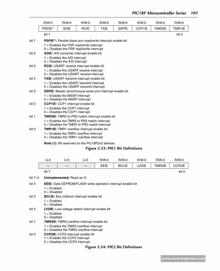
Figure 2.54: Pie2 Bit definitions
U-0 U-0 U-0 R/W-0 R/W-0 R/W-0 R/W-0 R/W-0
— — — EEIE BCLIE LVDIE TMR3IE CCP2IE
bit 7 bit 0
bit 7–5 Unimplemented: Read as '0'
bit 4 EEIE: Data EEPROM/FLASH write operation interrupt enable bit 1 = Enabled 0 = Disabledbit 3 BCLIE: Bus collision interrupt enable bit 1 = Enabled 0 = Disabledbit 2 LVDIE: Low-voltage detect interrupt enable bit 1 = Enabled 0 = Disabledbit 1 TMR3IE: TMR3 overflow interrupt enable bit 1 = Enables the TMR3 overflow interrupt 0 = Disables the TMR3 overflow interruptbit 0 CCP2IE: CCP2 interrupt enable bit 1 = Enables the CCP2 interrupt 0 = Disables the CCP2 interrupt
Figure 2.53: Pie1 Bit definitions
R/W-0 R/W-0 R/W-0 R/W-0 R/W-0 R/W-0 R/W-0 R/W-0
PSPIE(1) ADIE RCIE TXIE SSPIE CCP1IE TMR2IE TMR1IE
bit 7 bit 0
bit 7 PSPIE(1): Parallel slave port read/write interrupt enable bit 1 = Enables the PSP read/write interrupt 0 = Disables the PSP read/write interruptbit 6 ADIE: A/D converter interrupt enable bit 1 = Enables the A/D interrupt 0 = Disables the A/D interruptbit 5 RCIE: USART receive interrupt enable bit 1 = Enables the USART receive interrupt 0 = Disables the USART receive interruptbit 4 TXIE: USART transmit interrupt enable bit 1 = Enables the USART transmit interrupt 0 = Disables the USART transmit interruptbit 3 SSPIE: Master synchronous serial port interrupt enable bit 1 = Enables the MSSP interrupt 0 = Disables the MSSP interruptbit 2 CCP1IE: CCP1 interrupt enable bit 1 = Enables the CCP1 interrupt 0 = Disables the CCP1 interruptbit 1 TMR2IE: TMR2 to PR2 match interrupt enable bit 1 = Enables the TMR2 to PR2 match interrupt 0 = Disables the TMR2 to PR2 match interruptbit 0 TMR1IE: TMR1 overflow interrupt enable bit 1 = Enables the TMR1 overflow interrupt 0 = Disables the TMR1 overflow interrupt
Note (1): Bit reserved on the PIC18F2x2 devices.
PIC18F Microcontroller series 101
www.newnespress.com
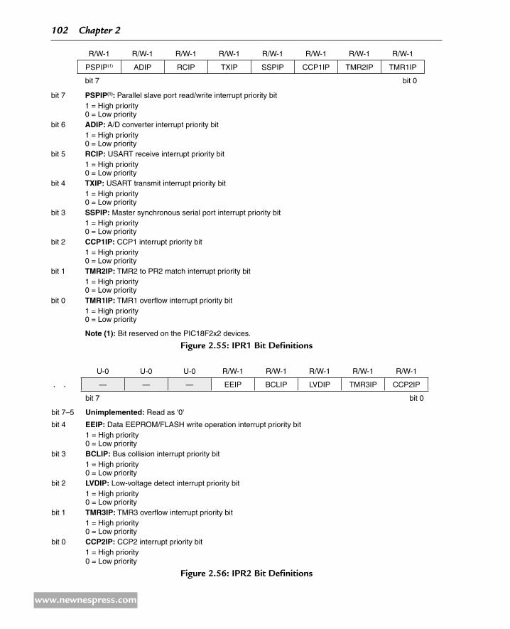
Figure 2.56: iPr2 Bit definitions
U-0 U-0 U-0 R/W-1 R/W-1 R/W-1 R/W-1 R/W-1
— — — EEIP BCLIP LVDIP TMR3IP CCP2IP
bit 7 bit 0
bit 7–5 Unimplemented: Read as '0'
bit 4 EEIP: Data EEPROM/FLASH write operation interrupt priority bit 1 = High priority 0 = Low prioritybit 3 BCLIP: Bus collision interrupt priority bit 1 = High priority 0 = Low prioritybit 2 LVDIP: Low-voltage detect interrupt priority bit 1 = High priority 0 = Low prioritybit 1 TMR3IP: TMR3 overflow interrupt priority bit 1 = High priority 0 = Low prioritybit 0 CCP2IP: CCP2 interrupt priority bit 1 = High priority 0 = Low priority
Figure 2.55: iPr1 Bit definitions
R/W-1 R/W-1 R/W-1 R/W-1 R/W-1 R/W-1 R/W-1 R/W-1
PSPIP(1) ADIP RCIP TXIP SSPIP CCP1IP TMR2IP TMR1IP
bit 7 bit 0
bit 7 PSPIP(1): Parallel slave port read/write interrupt priority bit 1 = High priority 0 = Low prioritybit 6 ADIP: A/D converter interrupt priority bit 1 = High priority 0 = Low prioritybit 5 RCIP: USART receive interrupt priority bit 1 = High priority 0 = Low prioritybit 4 TXIP: USART transmit interrupt priority bit 1 = High priority 0 = Low prioritybit 3 SSPIP: Master synchronous serial port interrupt priority bit 1 = High priority 0 = Low prioritybit 2 CCP1IP: CCP1 interrupt priority bit 1 = High priority 0 = Low prioritybit 1 TMR2IP: TMR2 to PR2 match interrupt priority bit 1 = High priority 0 = Low prioritybit 0 TMR1IP: TMR1 overflow interrupt priority bit 1 = High priority 0 = Low priority
Note (1): Bit reserved on the PIC18F2x2 devices.
102 Chapter 2
www.newnespress.com

example 2.3
Set up INT1 as a rising-edge triggered interrupt input having high priority.
solution
The following bits should be set up before the INT1 rising-edge triggered interrupts can be accepted by the CPU in the high-priority mode:
Enable priority structure. Set IPEN • = 1
Make INT1 an input pin. Set TRISB • = 1
Set INT1 interrupts for rising edge. SET INTEDG1 • = 1
Enable INT1 interrupts. Set INT1IE • = 1
Enable high priority. Set INT1IP • = 1
Clear INT1 flag. Set INT1IF • = 0
Enable all interrupts. Set GIEH • = 1
When an interrupt occurs, the CPU jumps to address 000018H of the program memory to execute the user program at the interrupt service routine.
2.2 Summary
This chapter has described the architecture of the PIC18F family of microcontrollers. PIC18F452 was considered as a typical example microcontroller in the family. Some other members of the family, such as the PIC18F242, have smaller pin counts and less functional-ity. In addition, some other members of the family, such as the PIC18F6680, have larger pin counts and more functionality.
Various important parts and peripheral circuits of the PIC18F series have been described, including the data memory, program memory, clock circuits, reset circuits, WDT, general-purpose timers, capture and compare module, PWM module, A/D converter, and the interrupt structure.
2.3 exercises
Describe the data memory structure of the PIC18F452 microcontroller. What is a bank? 1. How many banks are there?
Explain the differences between a general-purpose register (GPR) and a special function 2. register (SFR).
PIC18F Microcontroller series 103
www.newnespress.com

Explain the various ways that the PIC18F microcontroller can be reset. Draw a circuit 3. diagram to show how an external push-button switch can be used to reset the microcontroller.
Describe the various clock sources that can be used to provide clock to a PIC18F452 4. microcontroller. Draw a circuit diagram to show how a 10-MHz crystal can be connected to the microcontroller.
Draw a circuit diagram to show how a resonator can be connected to a PIC18F 5. microcontroller.
In a nontime-critical application, it is required to provide clock to a PIC18F452 6. microcontroller using an external resistor and a capacitor. Draw a circuit diagram to show how this can be done and find the component values if the required clock frequency is 5 MHz.
Explain how an external clock can be used to provide clock pulses to a PIC18F 7. microcontroller.
What are the registers of PORTA? Explain the operation of the port by drawing the port 8. block diagram.
It is required to set the WDT to provide automatic reset every 0.5 s. Describe how this 9. can be done and list the appropriate register bits.
It is required to generate PWM pulses from pin CCP1 of a PIC18F452 microcontroller. 10. The required pulse period is 100 µs, and the required duty cycle is 50%. Assuming that the microcontroller operates with a 4-MHz crystal, calculate the values to be loaded into various registers.
It is required to generate PWM pulses from pin CCP1 of a PIC18F452 microcontroller. 11. The required pulse frequency is 40 KHz, and the required duty cycle is 50%. Assuming that the microcontroller operates with a 4-MHz crystal, calculate the values to be loaded into various registers.
An LM35DZ type analog temperature sensor is connected to analog port AN0 of a 12. PIC18F452 microcontroller. The sensor provides an analog output voltage proportional to the temperature, i.e., Vo = 10 mV/°C. Show the steps required to read the temperature.
Explain the differences between a priority interrupt and a nonpriority interrupt.13.
Show the steps required to set up INT2 as a falling-edge triggered interrupt input having 14. low priority. What is the interrupt vector address?
Show the steps required to set up both INT1 and INT2 as falling-edge triggered interrupt 15. inputs having low priorities.
104 Chapter 2
www.newnespress.com

Show the steps required to set up INT1 as falling-edge triggered and INT2 as rising-edge 16. triggered interrupt inputs having high priorities. Explain how you can find the source of the interrupt when an interrupt occurs.
Show the steps required to set up Timer 0 to generate high-priority interrupts every 17. millisecond. What is the interrupt vector address?
In an application, the CPU registers have been configured to accept interrupts from 18. external sources INT0, INT1, and INT2. An interrupt has been detected. Explain how you can find the source of the interrupt.
PIC18F Microcontroller series 105
www.newnespress.com

This page intentionally left blank

ChaPter 3
Memory Cards
3.1 Memory Card types
A memory card (also called a flash memory card) is a solid-state electronic data storage device. First invented by Toshiba in the 1980s, memory cards save the stored data even after the memory device is disconnected from its power source. This ability to retain data is the key for flash memory card applications, for example, in digital cameras, where the saved pictures are not lost after the memory card is removed from the camera.
Nowadays, memory cards are used in consumer electronics and industrial applications. In consumer devices, we see the use of memory cards in applications like
Personal computers •
Digital cameras •
Mobile phones •
Video cameras •
Notebook computers •
Global positioning systems •
MP3 players •
Personal digital assistants •
In industrial applications, we see the use of memory cards in
Embedded computers •
Networking products •
Military systems •
Communication devices •
Medical products •
107© 2010 Elsevier Ltd. All rights reserved.D.O.I.: 10.1016/B978-1-85617-719-1.00007-5

Security systems •
Handheld scanners •
Memory cards are based on two technologies: NOR technology and NAND technology. NOR technology provides high-speed random access capabilities, where data as small as a single byte can be retrieved. NOR technology-based memory cards are often found in mobile phones, personal digital assistants, and computers. NAND technology was invented after the NOR technology, and it allows sequential access to the data in single pages but cannot retrieve single bytes of data like NOR flash. NAND technology-based memory cards are commonly found in digital cameras, mobile phones, audio and video devices, and other devices where the data is written and read sequentially.
There are many different types of memory cards available in the market. Some of the most commonly known memory cards are
Smart media (SM) card •
Multimedia card (MMC) •
Compact flash (CF) card •
Memory stick (MS) card •
Microdrive •
xD card •
Secure digital (SD) card •
The specifications and details of each card are summarized in the following sections.
3.2 Smart Media Card
The SM card was first developed in 1995 by Toshiba and was also called the Solid State Floppy Disc Card (SSFDC). The SM card consists of a single NAND flash chip embedded in a thin plastic card, and it is the thinnest card of all. Figure 3.1 shows a typical SM card. The dimensions of the card are 45.0 × 37.0 × 0.76 mm, and it weighs only 1.8 g. The card consists of a flat electrode terminal with 22 pins.
The SM card was mainly used in Fuji and Olympus cameras, where it had approximately 50% of the memory card share in 2001. The capacities of these cards ranged from 0.5 to 128 MB, and the data transfer rate was approximately 2 MB/s. SM cards started having problems as camera resolution increased considerably and cards greater than 128 MB were
108 Chapter 3
www.newnespress.com

not available. SM cards were designed to operate at either 3.3 or 5 V, and a small notched corner was used to protect 3.3-V cards from being inserted into 5-V readers.
SM cards incorporated a copy protection mechanism known as the “ID,” which gave every card a unique identification number for use with copy protection systems.
SM cards are no longer manufactured, and Fujifilm and Olympus both switched to xD cards. Now, no devices are designed to use SM cards, but 128-MB cards for old devices can still be obtained from memory card suppliers.
3.3 Multimedia Card
MMCs were first developed in the late 1970s by Intgenix and SanDisk. These cards were initially used in mobile phone and pager devices, but today they are commonly used in many other electronic devices. MMCs are backward compatible with SD cards, and they can be plugged into SD card slots. The reverse is not possible because SD cards are thicker (2.1 mm) and will not fit into MMC slots. Figure 3.2 is a picture of a typical MMC. The card dimensions are 24.0 × 32.0 × 1.4 mm and it has 8 pins.
The MMC operating voltage is 3.3 V, and the data transfer rate is approximately 2.5 MB/s. MMCs are available with capacities up to 4 GB. The older MMCs have been replaced by new multimedia mobile cards. These cards offer higher performance than older MMCs, and they offer lower working voltages (1.8–3.3 V) to reduce power consumption in portable devices.
Figure 3.1: Smart Media Card
Figure 3.2: Multimedia Card
Memory Card 109
www.newnespress.com

3.4 Compact Flash Card
CF cards were first developed in 1994 by SanDisk. These are the cards offering the highest capacities, from 2 MB to 100 GB. Today, CF cards are used in expensive professional digital cameras and other professional mass storage devices. Low-capacity cards (up to 2 GB) use the FAT16 filing system, and cards with capacities higher than 2 GB use the FAT32 filing system.
There are two versions of CF cards: Type I and Type II. The only physical difference between the two types is that Type II cards are thicker than Type I cards. Type I card dimensions are 43.0 × 36.0 × 3.3 mm and Type II cards are 43.0 × 36.0 × 5.0 mm. Both cards have 50 pins. The Type I interface can supply up to 70 mA to the card, and the Type II interface can supply up to 500 mA. The card operating voltage is 3.3 or 5 V. Figure 3.3 shows a typical CF card.
There are four speeds of CF cards: a Standard CF, a CF High Speed (CF 2.0 with a data transfer rate of 16 MB/s), a faster CF 3.0 with a data transfer rate of 66 MB/s, and the fastest CF 4.0 standard with a data transfer rate of 133 MB/s. A future version of the CF cards, known as CFast, will be based on the Serial ATA bus with an expected speed of 300 MB/s.
The memory card speed is usually specified using the “x” rating. This is the speed of the first audio CD-ROM, which was 150 KB/s. For example, a card with a speed of 10x corresponds to a data transfer rate of 10 × 150 KB/s = 1.5 MB/s. Table 3.1 lists some of the commonly used speed ratings in memory cards.
The advantages of CF cards are as follows:
CF cards are rugged and more durable than other types of cards, and they can withstand •more physical damage than other cards.
CF cards are available at very high storage capacities. •
CF cards operate at high speeds. •
CF cards are compatible with the IDE/ATA hard-disk standards, and thus they can be •used in many embedded systems to replace hard disks.
Besides the advantages, the CF cards have some disadvantages, such as lack of a mechanical write protection switch or notch, and its large dimensions in comparison with other cards limit its use in slim devices.
Figure 3.3: Compact Flash Card
110 Chapter 3
www.newnespress.com

3.5 Memory Stick Card
The MS cards were first developed by Sony in 1998. Although the original MS was only 128 MB, the largest capacity currently available is 16 GB. Figure 3.4 shows a typical MS card.
The original MS, although it is not manufactured any more, is approximately the size and thickness of a stick of chewing gum. MS has now been replaced with Memory Stick PRO, Memory Stick Duo, and Memory Stick PRO-HG.
Memory Stick PRO was introduced in 2003 as a joint effort between Sony and SanDisk, and it allows a greater storage capacity and faster file transfer rate than the original MS.
Memory Stick Duo was developed as a result of the need for smaller and faster memory cards. It is smaller than the standard MS card, but an adapter allows it to be used in original MS applications.
Memory Stick PRO-HG was developed by Sony and SanDisk together in 2006. The data transfer speed of this card is 60 MB/s, which exceeds the speeds of all previous memory cards and is approximately three times faster than the Memory Stick PRO cards.
table 3.1: Memory Card Speed ratings
Speed rating Speed (MB/s)
6x 0.9
32x 4.8
40x 6.0
66x 10.0
100x 15.0
133x 20.0
150x 22.5
200x 30.0
266x 40.0
300x 45.0
Figure 3.4: Memory Stick Card
Memory Card 111
www.newnespress.com

3.6 Microdrive
Microdrive is basically a hard disk designed to fit into a Type II CF card size enclosure. Although the size of a microdrive is same as that of a CF card, its power consumption is much higher than flash memories and therefore cannot be used in low-power applications. The capacity of microdrives is 8 GB or more. Figure 3.5 shows a typical microdrive.
The physical dimensions of microdrives are 42.8 × 36.4 × 5.0 mm, and they weigh approximately 16 g. The first microdrive was developed by IBM in 1999 with a capacity of 170 and 340 MB. Soon after, the capacity was increased to greater than 2 GB in the year 2003 by Hitachi. Microdrives with a capacity of 8 GB were introduced in 2008 by Hitachi and Seagate.
The advantage of microdrives is that they allow more write cycles than the memory cards. In addition, microdrives are better at handling power loss in the middle of writing. One of the disadvantages of microdrives is that they do not survive if dropped from a height of 1.2 m. In addition, their transfer speeds are around 5 MB/s, which is lower than most of the present day high-end memory cards. In addition, they are not designed to operate at high altitudes, and their power consumption is high compared with memory cards.
3.7 xd Card
xD stands for extreme Digital, and these cards are mainly used in digital cameras, digital voice recorders, and MP3 players. xD cards were developed by Olympus and Fujifilm in 2002 and then manufactured by Toshiba Corporation and Samsung Electronics. Figure 3.6 is a picture of a typical xD card. xD cards are available in three types: Type M, Type H, and Type M+.
Figure 3.5: Microdrive
Figure 3.6: xd Card
112 Chapter 3
www.newnespress.com

Type M cards were developed in 2005 and are available in capacities up to 2 GB. The read and write speeds of these cards are 4 and 2.5 MB/s, respectively.
Type H xD cards were first released in 2005 have the advantage of a higher data transfer speed. These cards are also available in capacities up to 2 GB with read and write speeds of 5 and 4 MB/s, respectively. Unfortunately, the production of Type H cards has now been discontinued due to their high production costs.
Type M+ xD cards were first released in 2008, and their capacities are up to 2 GB. These cards are the fastest xD cards, with read and write speeds of 6 and 3/75 MB/s, respectively.
The advantage of xD cards is that they are faster than SM cards, MMCs, and MS cards. In addition, their small size makes them attractive in portable low-power applications. Some of the disadvantages of xD cards are their higher cost, bigger size than some other memory cards (such as microSD), and the fact that they are proprietary to Fujifilm and Olympus. This means that there is no publicly available documentation on their design and implementation.
3.8 Secure digital Card
SD cards are probably the most widely used memory cards today. The SD card was originally developed by Matsushita, SanDisk, and Toshiba in 2000. SD cards nowadays a used in many portable devices, such as digital cameras, mobile phones, PDAs, handheld computers, video recorders, GPS receivers, video game consoles, and so on.
Standard SD cards are available with capacities from 4 MB to 4 GB. Recently, a new type of SD card called the high-capacity SD card (SDHC) has been developed with capacities ranging from 4 to 32 GB. It has been announced that a new specification called eXtended Capacity (SDXC) will allow capacities to reach 2 TB.
SD cards are based on MMC, but they have a number of differences: SD cards are physically thicker than MMCs and would not fit into MMC slots. The MMC, on the other hand, can be easily inserted into SD card slots. In addition, SD cards are shaped asymmetrically to prevent them being inserted upside down, whereas an MMC would go in either direction, although it will not make contact if inserted upside down. In addition, the internal register structures of the two types of cards are not the same.
381 standard sD Cards
SD cards are available in three different sizes: normal SD, miniSD, and microSD. Figure 3.7 shows the three types of SD cards.
Normal SD cards have the dimensions 24.0 × 32.0 × 2.1 mm and a weight of 2 g. A write-protect switch is provided on the card to stop accidental deletion of the contents of
Memory Card 113
www.newnespress.com
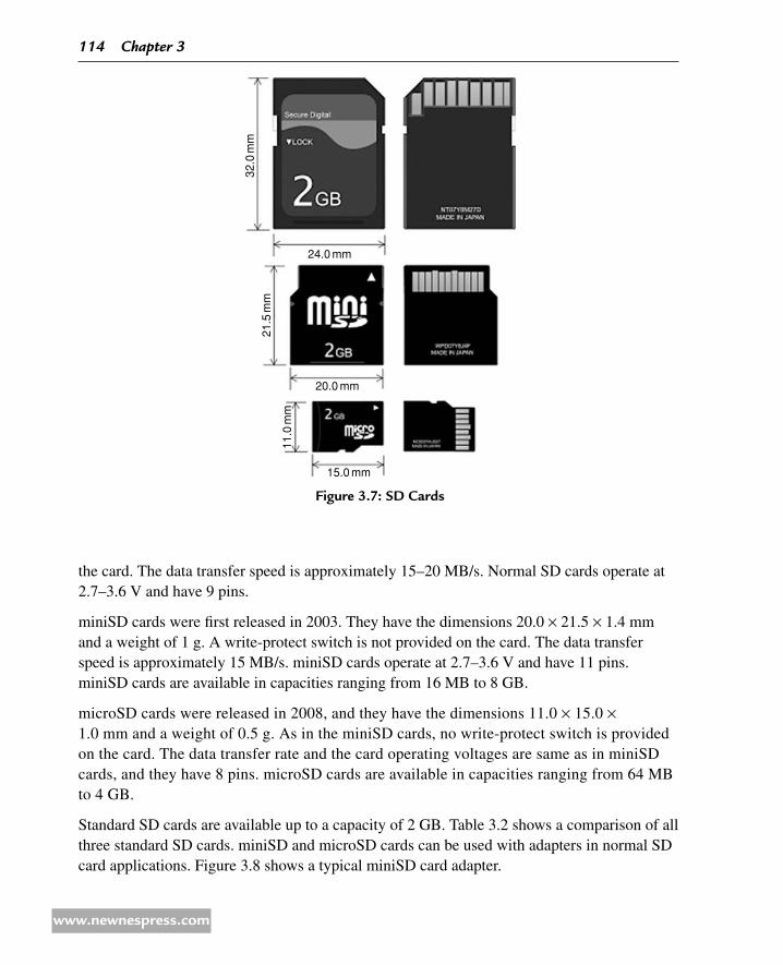
the card. The data transfer speed is approximately 15–20 MB/s. Normal SD cards operate at 2.7–3.6 V and have 9 pins.
miniSD cards were first released in 2003. They have the dimensions 20.0 × 21.5 × 1.4 mm and a weight of 1 g. A write-protect switch is not provided on the card. The data transfer speed is approximately 15 MB/s. miniSD cards operate at 2.7–3.6 V and have 11 pins. miniSD cards are available in capacities ranging from 16 MB to 8 GB.
microSD cards were released in 2008, and they have the dimensions 11.0 × 15.0 × 1.0 mm and a weight of 0.5 g. As in the miniSD cards, no write-protect switch is provided on the card. The data transfer rate and the card operating voltages are same as in miniSD cards, and they have 8 pins. microSD cards are available in capacities ranging from 64 MB to 4 GB.
Standard SD cards are available up to a capacity of 2 GB. Table 3.2 shows a comparison of all three standard SD cards. miniSD and microSD cards can be used with adapters in normal SD card applications. Figure 3.8 shows a typical miniSD card adapter.
24.0 mm32
.0m
m
20.0 mm
15.0 mm
21.5
mm
11.0
mm
Figure 3.7: Sd Cards
114 Chapter 3
www.newnespress.com

Standard SD cards (up to 2 GB) are usually shipped with the FAT16 file system preloaded on the card.
382 High-Capacity sD Cards
Secure Digital SDHC was released in 2006 and is an extension of the standard SD card format. SDHC cards provide capacities f 2 GB up to 32 GB. It is important to realize that although the SDHC cards have the same physical dimensions as the standard SD cards, they use different protocols and as such will only work in SDHC-compatible devices and not in standard SD card applications. SDHC cards should not be used in standard SD compatible devices. Standard SD cards are, however, forward compatible with SDHC host devices, making standard SD cards compatible with both SD and SDHC host devices.
SDHC cards offer
Larger data capacities •
Larger number of files •
FAT32 filing system (instead of the FAT16) •
Higher data transfer rates •
Content protection for recordable media (CPRM) copyright protection •
Standard SD card physical size compatibility •
Figure 3.8: miniSd Card adapter
table 3.2: Comparison of Standard Sd Cards
Property Sd miniSd microSd
Width 24 mm 20 mm 11 mm
Length 32 mm 21.5 mm 15 mm
Thickness 2.1 mm 1.4 mm 1 mm
Weight 2 g 1 g 0.5 g
Operating voltage 2.7–3.6 V 2.7–3.6 V 2.7–3.6 V
No. of pins 9 11 8
Memory Card 115
www.newnespress.com
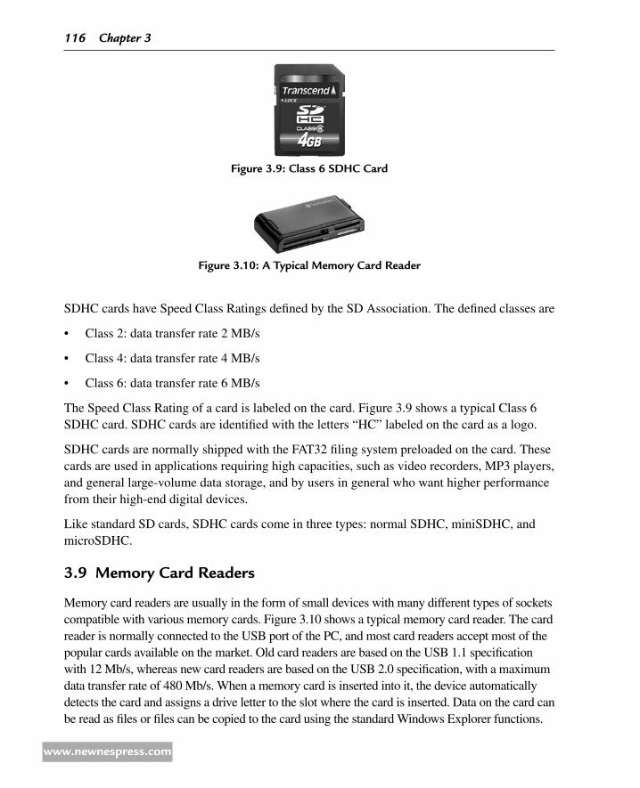
SDHC cards have Speed Class Ratings defined by the SD Association. The defined classes are
Class 2: data transfer rate 2 MB/s •
Class 4: data transfer rate 4 MB/s •
Class 6: data transfer rate 6 MB/s •
The Speed Class Rating of a card is labeled on the card. Figure 3.9 shows a typical Class 6 SDHC card. SDHC cards are identified with the letters “HC” labeled on the card as a logo.
SDHC cards are normally shipped with the FAT32 filing system preloaded on the card. These cards are used in applications requiring high capacities, such as video recorders, MP3 players, and general large-volume data storage, and by users in general who want higher performance from their high-end digital devices.
Like standard SD cards, SDHC cards come in three types: normal SDHC, miniSDHC, and microSDHC.
3.9 Memory Card readers
Memory card readers are usually in the form of small devices with many different types of sockets compatible with various memory cards. Figure 3.10 shows a typical memory card reader. The card reader is normally connected to the USB port of the PC, and most card readers accept most of the popular cards available on the market. Old card readers are based on the USB 1.1 specification with 12 Mb/s, whereas new card readers are based on the USB 2.0 specification, with a maximum data transfer rate of 480 Mb/s. When a memory card is inserted into it, the device automatically detects the card and assigns a drive letter to the slot where the card is inserted. Data on the card can be read as files or files can be copied to the card using the standard Windows Explorer functions.
Figure 3.9: Class 6 SdhC Card
Figure 3.10: a typical Memory Card reader
116 Chapter 3
www.newnespress.com

3.10 Memory Card Physical Properties
Table 3.3 gives a comparison of the physical properties of commonly used memory cards. As can be seen from the table, the microSD card has the smallest form factor.
3.11 Memory Card technical Properties
Table 3.4 gives a comparison of the technical properties of commonly used memory cards.
table 3.3: Physical Properties of Memory Cards
Card Width (mm) Length (mm) thickness (mm) Weight (g)
CF – Type I 43.0 36.0 3.3 3.3
CF – Type II 43.0 36.0 5.0 5.0
SM 37.0 45.0 0.76 2.0
MMC 24.0 32.0 1.4 1.3
RS-MMC 24.0 16.0 1.4 1.3
MMC-micro 14.0 12.0 1.1 1.0
MS 21.5 50.0 2.8 4.0
MS PRO Duo 20.0 31.0 1.6 2.0
SD 24.0 32.0 2.1 2.0
miniSD 20.0 21.5 1.4 0.5
microSD 15.0 11.0 1.0 0.27
xD 25.0 20.0 1.78 2.8
table 3.4: technical Properties of Memory Cards
CardMax Capacity
(2009)Max Write
Speed (MB/s)Max read
Speed (MB/s)Operating
Voltage (V) Pin Count
CF – Type I 32 GB 133 133 3.5 and 5.0 50
CF – Type II 32 GB 133 133 3.3 and 5.0 50
SM 128 MB 20 20 3.3 and 5.0 22
MMC 4 GB 52 52 3.3 7
RS-MMC 2 GB 52 52 3.3 7
MMC micro 2 GB 40 40 3.3 13
MS 128 MB 160 160 3.3 10
MS PRO Duo 16 GB 160 160 3.3 10
SD 4 GB 150 150 3.3 9
miniSD 4 GB 100 100 3.3 11
microSD 4 GB 100 100 3.3 8
SDHC 64 GB 48 48 3.3 9
Memory Card 117
www.newnespress.com

3.12 detailed Sd Card Structure
As the topic of this book is SD cards, the internal structure and the use of these cards in PIC microcontroller-based systems will be described in this section.
3121 sD Card Pin Configuration
Figure 3.11 shows the pin configuration of a standard SD card. The card has nine pins, as shown in the figure, and a write-protect switch to enable/disable writing onto the card.
A standard SD card can be operated in two modes: the SD Bus mode and the SPI Bus mode. SD Bus mode is the native operating mode of the card, and all the pins are used in this mode. Data is transferred using four pins (D0–D3), a clock (CLK) pin, and a command line (CMD). Data can be transferred from the card to the host or vice versa over the four data lines. Figure 3.12 shows the SD card connection in SD Bus mode.
SPI Bus mode is the more commonly used mode, and it allows data to be transferred on two lines (DO and DI) in serial format using a chip select (CS) and a CLK line. The SPI mode is easier to use, but it has the disadvantage of reduced performance compared with the SD mode of operation. Figure 3.13 shows the SD card connections in SPI mode.
SD card pins have different meanings depending upon the mode of operation. Table 3.5 shows the pin assignments when the card is operated in SD Bus and SPI Bus modes.
The projects in this book are based on the operations in the SPI Bus mode. The following pins are used in SPI Bus mode:
Chip select – Pin 1 •
Data in – Pin 2 •
Clock – Pin 5 •
Data out – Pin 7 •
Figure 3.11: Standard Sd Card Pin Configuration
87654321
9
118 Chapter 3
www.newnespress.com

In addition, pin 4 must be connected to the supply voltage, and pins 3 and 6 must be connected to the supply ground.
3122 sD Card Interface
Before we can use an SD card in an electronic circuit, we have to know the interface signal levels. Table 3.6 shows the input–output voltage levels of the standard SD cards.
According to Table 3.6,
Minimum logic 1 output voltage, VOH = 2.475 V
Figure 3.12: Sd Card in Sd Bus Mode
Microcontroller
CLK
D0-D3
D0-D3
SD card
SD card
SD card
Vss
Vdd
D0-D3
CMD
CMD
CMD
Memory Card 119
www.newnespress.com

Figure 3.13: Sd Card in SPi Bus Mode
CS
D0, D1, CLK
CS
D0, D1, CLK
CS
D0, D1, CLK
Microcontroller
SD card
SD card
SD card
Vss
Vdd
table 3.5: Sd Card Pin assignments
Pin No Name Sd Mode SPi Mode
1 CD/DAT3 Card detect/Data line Chip select
2 CMD Command response Data in
3 Vss Ground Ground
4 Vdd Supply voltage Supply voltage
5 CLK Clock Clock
6 Vss Ground Ground
7 DAT0 Data line Data out
8 DAT1 Data line Reserved
9 DAT2 Data line Reserved
120 Chapter 3
www.newnespress.com

Maximum logic 0 output voltage, VOL = 0.4125 V
Minimum required logic 1 input voltage, VIH = 2.0625 V
Maximum logic 1 input voltage = 3.6 V
Maximum required logic 0 input voltage, VIL = 0.825 V
When connected to a PIC microcontroller, the output voltage (2.475 V) of the SD card is enough to drive the input circuit of the microcontroller. The typical logic 1 output voltage of a PIC microcontroller pin is 4.3 V, and this is too high when applied as an input to a microcontroller pin, where the maximum voltage should not exceed 3.6 V. As a result of this, it is required to use resistors at the inputs of the SD card to lower the input voltage. Figure 3.14 shows a typical SD card interface to a PIC microcontroller. In this figure, 2.2- and 3.3-K resistors are used as a potential divider circuit to lower the SD card input voltage to approximately 2.48 V, as shown below.
SD card input voltage = 4.3 V × 3.3 K / (2.2 K + 3.3 K) = 2.48 V.
In Figure 3.14, the SD card is connected to PORTC pins of the microcontroller as follows:
Sd Card Pin Microcontroller Pin
CS RC2
CLK RC3
DO RC4
DI RC5
This is the recommended connection because it uses the SPI Bus port pins of the microcontroller (RC3, RC4, and RC5).
table 3.6: Sd Card input–Output Voltage Levels
Symbol Minimum Maximum
Logic 1 output voltage VOH 0.75 × Vdd
Logic 0 output voltage VOL 0.125 × Vdd
Logic 1 input voltage VIH 0.625 × Vdd Vdd + 0.3
Logic 0 input voltage VIL Vss − 0.3 0.25 × Vdd
Memory Card 121
www.newnespress.com

SD cards support “hot” insertion of the card, i.e., the card can be inserted into the circuit without powering down the host. This is usually achieved through the card connector. Connector manufacturers usually provide sockets that have power pins long enough to power the card before any contact is made with the other pins.
A feature of most SD cards is the automatic entry and exit from sleep mode. After an operation, cards usually enter a sleep mode to conserve power-in, if no more commands are received within 5 ms. Although the host does not need to do anything for this to happen, it is recommended that the host shut the clock generation. Any command sent to the card will force it to exit from the sleep mode.
SD cards can consume up to 100–200 mA while reading or writing onto the card. This is usually a high current, and an appropriate voltage regulator capable of supplying the required current must be used in the design. The card consumes approximately 150 µA in sleep mode.
3.13 Sd Card internal registers
The operations of SD cards are controlled by a number of internal registers. Some registers are 16 bits wide, some are 32 bits wide, and some are 128 bits wide. Table 3.7 gives a list of all the registers.
Detailed information on the functions and bit definitions of all the registers can be found in the product manuals of card manufacturers (e.g., SanDisk Secure Digital Card, Product Manual, Document no: 80-13-00169, 2003). The details of the important registers and their bit definitions are given in this section.
Figure 3.14: PiC Microcontroller Sd Card interface
VddPIC
Vss2
3,6
3.3 K
7
51
CS
2.2 K
3.3 K
2.2 KRC2RC3RC4
RC5
SD card
3.6 V 2.48 V
CLKDODI
122 Chapter 3
www.newnespress.com
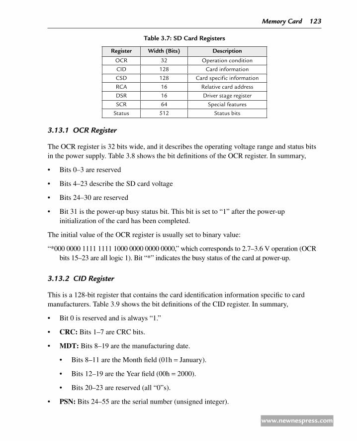
3131 OCR Register
The OCR register is 32 bits wide, and it describes the operating voltage range and status bits in the power supply. Table 3.8 shows the bit definitions of the OCR register. In summary,
Bits 0–3 are reserved •
Bits 4–23 describe the SD card voltage •
Bits 24–30 are reserved •
Bit 31 is the power-up busy status bit. This bit is set to “1” after the power-up •initialization of the card has been completed.
The initial value of the OCR register is usually set to binary value:
“*000 0000 1111 1111 1000 0000 0000 0000,” which corresponds to 2.7–3.6 V operation (OCR bits 15–23 are all logic 1). Bit “*” indicates the busy status of the card at power-up.
3132 CID Register
This is a 128-bit register that contains the card identification information specific to card manufacturers. Table 3.9 shows the bit definitions of the CID register. In summary,
Bit 0 is reserved and is always “1.” •
• CRC: Bits 1–7 are CRC bits.
• MDT: Bits 8–19 are the manufacturing date.
Bits 8–11 are the Month field (01h • = January).
Bits 12–19 are the Year field (00h • = 2000).
Bits 20–23 are reserved (all “0”s). •
• PSN: Bits 24–55 are the serial number (unsigned integer).
table 3.7: Sd Card registers
register Width (Bits) description
OCR 32 Operation condition
CID 128 Card information
CSD 128 Card specific information
RCA 16 Relative card address
DSR 16 Driver stage register
SCR 64 Special features
Status 512 Status bits
Memory Card 123
www.newnespress.com

table 3.8: OCr register Bit definitions
OCr Bit Card Voltage initial Value
31 Card busy bit “0” = busy, “1” = ready
30–24 Reserved All “0”s
23 3.6–3.5 1
22 3.5–3.4 1
21 3.4–3.3 1
20 3.3–3.2 1
19 3.2–3.1 1
18 3.1–3.0 1
17 3.0–2.9 1
16 2.9–2.8 1
15 2.8–2.7 1
14 2.7–2.6 0
13 2.6–2.5 0
12 2.5–2.4 0
11 2.4–2.3 0
10 2.3–2.2 0
9 2.2–2.1 0
8 2.1–2.2 0
7 2.0–1.9 0
6 1.9–1.8 0
5 1.8–1.7 0
4 1.7–1.6 0
3–0 Reserved All “0”s
table 3.9: Cid register Bit definitions
Field Width Bit Position description
MID 8 127–120 Manufacturer’s ID
OID 16 119–104 Card OEM
PNM 40 103–64 Product code
PRV 8 63–56 Product revision
PSN 32 55–24 Serial number
— 4 23–20 0
MDT 12 19–8 Manufacturing date
CRC 7 7–1 Checksum
— 1 0 1
124 Chapter 3
www.newnespress.com

• PRV: Bits 56–63 are the Product Revision of the card.
• PNM: Bits 64–103 are the 5-ASCII-character Product Code, for example,
SD064 is 64 MB card. •
SD128 is 128 MB card. •
SD256 is 256 MB card. •
• OID: Bits 104–119 are the card OEM, allocated by the SD Card Association, for example,
TM indicates Toshiba. •
SD indicates SanDisk. •
• MID: Bits 120–127 are the Manufacturer’s ID, for example,
02h indicates Toshiba. •
03h indicates SanDisk. •
As an example, the Toshiba 64-MB card has the following initial values in its 128-bit CID register (in hexadecimal, “*” depends on the card, and “#” depends on values on the card):
MID: 02
OID: 54 4D
PNM: 53 44 30 36 34
PRV: * *
PSN: * * * * * * * *
0
MDT: * * *
CRC: # #
3133 CsD Register
CSD is the 128-bit Card Specific Data register that contains information required to access the data on the card. Some fields of the CSD register are read only, whereas some other fields are writeable. Table 3.10 shows bit definitions of the CSD register. In summary,
• CSD_STRUCTURE: Bits 126–127 are the CSD structure version number.
Bits 120–125 are reserved (all “0”). •
Memory Card 125
www.newnespress.com

table 3.10: CSd register Bit definitions
Field description Width Bits *Value Code
CSD_STRUCTURE CSD structure 2 127–126 1.0 00b
— 6 125–120 — 000000b
TAAC Data read access time 8 119–112 10 ms 00001111b
NSAC Data read access time 8 111–104 0 00000000b
TRAN_SPEED Max data transfer rate 8 103–96 25 MHz 00110010b
CCC Command classes 12 95–84 All 1F5h
READ_BL_LEN Max read block length 4 83–80 512 bytes 1001h
READ_BL_PARTIAL Partial read blocks allowed 1 79–79 Yes 1b
WRITE_BLK_MISALIGN Write block misalignment 1 78–78 No 0b
READ_BLK_MISALIGN Read block misalignment 1 77–77 No 0b
DSR_IMP DSR implemented 1 76–76 No 0b
— Reserved 2 75–74 — 00b
C_SIZE Device size 12 73–62 899 383h
VDD_R_CURR_MIN Max. Read current at Vdd min 3 61–59 100 mA 111b
VDD_R_CURR_MAX Max. Read current at Vdd max 3 58–56 80 mA 110b
VDD_W_CURR_MIN Max. Write current at Vdd min 3 55–53 100 mA 111b
VDD_W_CURR_MAX Max. Write current at Vdd max
3 52–50 80 mA 110b
C_SIZE_MULT Device size multiplier 3 49–47 32 011b
ERASE_BLK_EN Erase single block enable 1 46–46 Yes 1b
SECTOR_SIZE Erase sector size 7 45–39 32 blocks 0011111b
WP_GRP_SIZE Write protect group size 7 38–32 128 sectors
1111111b
WP_GRP_ENABLE Write protect group enable 1 31–31 Yes 1b
— Reserved 2 30–29 — 00b
R2W_FACTOR Write speed factor 3 28–26 X16 100b
3 28–26 X4 010b
WRITE_BL_LEN Max write block length 4 25–22 512 bytes 1001b
WRITE_BL_PARTIAL Partial write allowed 1 21–21 No 0b
— Reserved 5 20–16 — 00000b
FILE_FORMAT_GRP File format group 1 15–15 0 0b
COPY Copy flag 1 14–14 Not original
0b
PERM_WRITE_PROTECT Permanent write protection 1 13–13 Not protected
0b
TMP_WRITE_PROTECT Temporary write protection 1 12–12 Not protected
0b
FILE_FORMAT File format 2 11–10 HD w/partition
00b
— Reserved 2 9–8 — 00b
126 Chapter 3
www.newnespress.com

• TAAC: Bits 112–119 define the asynchronous part of the read access time of the card. The bits are decoded as follows:
TAAC bit Code2–0 Time unit. 0 = 1 ns, 1 = 10 ns, 2 = 100 ns, 3 = 1 μs, 4 = 10 μs, 5 = 100 μs6–3 Time value. 0 = Reserved, 1 = 1.0, 2 = 1.2, 3 = 1.3, 4 = 1.5, 5 = 2.0, 6 = 2.5, 7 = 3.0, 8 = 3.5, 9 = 4.0, A = 4.5, B = 5.0, C = 5.5, D = 6.0, e = 7.0, F = 8.07 Reserved
• NSAC: Bits 104–111 define the worst case for the clock-dependent factor of the data access time. The unit is 100 clock cycles. The total access time is equal to TAAC plus NSAC.
• TRAN_SPEED: Bits 96–103 define the maximum data transfer rate. The bits are decoded as follows:
TRAN_SPEED bit Code2–0 Transfer Rate Unit. 0 = 100 kb/s, 1 = 1 Mb/s, 2 = 10 Mb/s, 3 = 100 Mb/s, 4–7 = Reserved6–3 Time Value. 0 = Reserved, 1 = 1.0, 2 = 1.2, 3 = 1.3, 4 = 1.5, 5 = 2.0, 6 = 2.5, 7 = 3.0, 8 = 3.5, 9 = 4.0, A = 4.5, B = 5.0, C = 5.5, D = 6.0, e = 7.0, F = 8.07 Reserved
• CCC: Bits 84–95 define the command classes that are supported by the card. The bit definitions are as follows:
CCC bit Supported card command class0 Class 01 Class1
Field description Width Bits *Value Code
CRC CRC 7 7–1 —
— Always 1 1 0–0 — 1b
*values are based on a 16 MB SanDisk card.
table 3.10: CSd register Bit definitions —cont’d
Memory Card 127
www.newnespress.com

… …11 Class 11
• READ_BL_LEN: Bits 80–83 define the maximum read data block length, which is equal to 2READ_BL_LEN. The data block length is specified as follows:
READ_BL_LEN Block Length0–8 Reserved9 29 = 512 bytes… …10 211 = 2048 bytes12–15 Reserved
Bit 79 is always “1.” •
• WRITE_BLK_MISALIGN: Bit 78 defines whether the data block to be written by one command can be spread over more than one physical block:
WRITE_BLK_MISALIGN Access Block boundary write0 Not allowed1 Allowed
• READ_BLK_MISALIGN: Bit 77 defines whether the data block to be read by one command can be spread over more than one physical block:
READ_BLK_MISALIGN Access Block boundary read0 Not allowed1 Allowed
• DSR_IMP: Bit 76, if set, a driver stage register (DSR) is implemented.
Bits 74–75 are reserved. •
• C_SIZE: Bits 62–73 define the user’s data card capacity as follows:
Memory capacity = BLOCKNR * BLOCK_LEN,
where
BLOCKNR = (C_SIZE + 1) * MULT
MULT = 2C_SIZ_MULT + 2 if C_SIZE_MULT < 8
and
BLOCK_LEN = 2READ_BL_LEN if READ_BL_LEN < 12.
Bits 50–61 define the maximum and minimum values for read/write currents •
128 Chapter 3
www.newnespress.com

• C_SIZE_MULT: Bits 47–49 are used to compute the user’s data card capacity multiply factor:
C_SIZE_MULT MULT0 22 = 41 23 = 82 24 = 163 25 = 324 26 = 645 27 = 1286 28 = 2567 29 = 512
• ERASE_BLK_EN: Bit 46 defines if host can erase by WRITE_BL_LEN:
ERASE_BLK_EN Description0 Host cannot erase by WRITE_BL_LEN1 Host can erase by WRITE_BL_LEN
• SECTOR_SIZE: Bits 39–45 define the minimum erasable size as the number of write blocks.
• WP_GRP_SIZE: Bits 32–38 define the minimum number of sectors that can be set for the write protect group.
• WP_GRP_ENABLE: Bit 31 defines the write protect group functions:
WP_GRP_ENABLE Description0 Not implemented1 Implemented
Bits 29–30 are reserved. •
• R2W_FACTOR: Bits 26–28 define a multiple number for a typical write time as a multiple of the read access time.
• WRITE_BL_LEN: Bits 22–25 define the maximum write block length, which is calculated as 2WRITE_BL_LEN. The data block length is specified as follows:
WRITE_BL_LEN Block Length0–9 Reserved11 29 = 512 bytes… …12 211 = 2048 bytes12–16 Reserved
Memory Card 129
www.newnespress.com

• WRITE_BL_PARTIAL: Bit 21 defines whether partial block write is available:
WRITE_BL_PARTIAL Write data size0 Only WRITE_BL_LEN size of 512 bytes is available1 Partial size write available
Bits 16–20 are reserved. •
• FILE_FORMAT_GRP: Bit 15 indicates the selected group of file format group and file format:
FILE_FORMAT_GRP FILE_FORMAT Kinds0 0 Hard disk-like file system with partition
table0 1 DOS FAT with boot sector only (no
partition table)0 2 Universal File Format0 3 Others1 0, 1, 2, 3 Reserved
• COPY: Bit 14 defines the contents of the card as original or duplicated. The bit definition is:
COPY Description
0 Original
1 Copy
• PERM_WRITE_PROTECT: Bit 13, if set, permanently write protects the card.
• TMP_WRITE_PROTECT: Bit 12, if set, temporarily write protects the card.
• FILE_FORMAT: Bits 10–11 define the file format on the card. This field is used together with field FILE_FORMAT_GRP as in the above table.
Bits 8–9 are reserved. •
• CRC: Bits 1–7 are the CRC error checking bits.
Bit 0 is not used and is always “1.” •
3134 RCA Register
This 16-bit register carries the card addresses in SD card mode.
3135 DsR Register
This register is not implemented in many cards.
130 Chapter 3
www.newnespress.com

3136 sCR Register
This 64-bit register provides information on the SD card’s special features, such as the structure version number, the physical layer specification, the security algorithm used, and the bus width.
3137 sD status Register
This 512-bit register defines the card status bits and card features.
3.14 Calculating the Sd Card Capacity
An example is given in this section to show how the capacity of an SD card can be calculated.
example 3.1
The following CSD register fields are given by a card manufacturer:
C_SIZE = E27h (or decimal 3623)C_SIZE_MULT = 3READ_BL_LEN = 9
Calculate the capacity of this card.
solution
The card capacity is defined by two fields within the CSD register: C_SIZE and C_SIZE_MULT. C_SIZE is a 12-bit value with an offset of 1 (1–4096), and C_SIZE_MULT is a 3-bit value with an offset of 2 (2–9).
The number of blocks on the card is given by
BLOCKNR = (C_SIZE + 1) × 2(C_SIZE_MULT + 2),
where
C_SIZE_MULT < 8.
The default block length is 512 bytes (but it can also be specified as 1024 or 2048 bytes). The block length is calculated from
BLOCK_LEN = 2READ_BL_LEN,
where
READ_BL_LEN = 9, 10, or 11.
Combining the two equations, we get the card capacity as
Card Capacity (in bytes) = BLOCKNR × BLOCK_LEN
Memory Card 131
www.newnespress.com
or
Card Capacity (in bytes) = (C_SIZE + 1) × 2 (C_SIZE_MULT + 2) × 2READ_BL_LEN.
The capacity is usually shown in MB and
Card Capacity (Megabyte) = (C_SIZE + 1) × 2(C_SIZE_MULT + 2) × 2 READ_BL_LEN/(1024 × 1024)
Using the CSD parameters given in this example, we get
Card Capacity (Megabyte) = 3624 × 32 × 512/(1024 × 1024) = 56.525 Megabytes
It is interesting to note that when a block length of 1024 bytes is used (READ_BL_LEN = 10), cards up to 2 GB can be specified, and with a block length of 2048 bytes (READ_BL_LEN = 11), cards up to 4 GB can be specified.
3.15 Sd Card SPi Bus Protocol
All communications between the host and the card are controlled by the host. Messages in the SPI bus protocol consist of commands, responses, and tokens. The card returns a response to every command received and also a data response token for every write command.
The SD card wakes up in SD card mode, and it will enter the SPI mode if its CS line is held low when a reset command is sent to the card. The card can only be returned to the SD mode after a power-down and power-up sequence.
When the SPI mode is entered, the card is in the nonprotected mode, where CRC checking is not used (CRC checking can be turned on and off by sending command CRC_ON_OFF, com-mand name CMD59, to the card).
3151 Data Read
Data can be read in either single or multiple blocks. The basic unit of data size is blocks, defined by field READ_BL_LEN of the CSD register. In this book, we shall be using only single-block reads. Single-block reads are initiated by issuing the command READ_SINGLE_BLOCK (CMD17) to the card. Any valid address can be used as the starting address.
3152 Data Write
Data can be written in either single or multiple blocks. After receiving a valid write command, the card sends a response token and then waits for the data block to be sent from the host. The starting address can be any valid address. After receiving a data block from the host, the card returns a data response token and writes the data on the card if the data contains no errors.
132 Chapter 3
www.newnespress.com

There are a large number of commands available in SPI mode for reading the card regis-ters, reading and writing single and multiple blocks of data, erasing blocks, etc. Table 3.11 gives a list of the important SD card commands. All SPI mode commands are 6 bytes long (48 bits). As shown in Table 3.12, the commands start with the most significant bit (MSB) as logic 0, a transmission bit as logic 1, 6 bits of command index, 32 bits of argument (not all commands need arguments), 7 bits of CRC, and an end-bit (logic 1). The commands are divided into classes. If no argument is required in a command, the value of the argument filed should be all “0”s. The command index contains the actual command number. For example, the command index value for command CMD8 is binary number 8 in 6 bits, i.e., “001000.”
3153 Response Tokens
There are several types of response tokens that can be sent by the card. A token is transmitted with the MSB bit sent first. The response tokens are as follows:
R1 Format: This response token is 1 byte long and is sent by the card after every command (except the SEND_STATUS command). The MSB bit is “0,” and other bits indicate an error (“1” bit). For example, if bit “0” is set, it indicates that the card is in Idle State and running initialization sequence. Table 3.13 shows bit definitions of the R1 Format.
R1b Format: This format is similar to R1 Format with the addition of the busy signal.
table 3.11: Some important Sd Card Commands
Command abbreviation argument response description
CMD0 GO_IDLE_STATE None R1 Reset the SD card
CMD1 SEND_OP_COND None R1 Initialize card
CMD9 SEND_CSD None R1 Get CSD register data
CMD10 SEND_CID None R1 Get CID register data
CMD17 READ_SINGLE_BLOCK Data address (0:31) R1 Read a block of data
CMD24 WRITE_BLOCK Data address (0:31) R1 Write a block of data
table 3.12: Command Format
Byte 1 Bytes 2–5 Byte 6
7 6 5 4 3 2 1 0 31.........................................0 7 6 5 4 3 2 1 0
0 1 Command Command argument CrC 1
Memory Card 133
www.newnespress.com

R2 Format: This response token is 2 bytes long and is sent as a response to command SEND_STATUS.
R3 Format: This response token is 5 bytes long and is sent in response to command READ_OCR. The first byte is identical to R1 format, whereas the other bytes contain the OCR register data.
Data Response Token: Whenever a data block is written to the card, the card acknowledges with a data response. This token is 1 byte long and has the following bit definitions:
Bit 0 Always 1Bits 1–2 StatusBit 3 Always 0Bit 4 Reserved
The Status bits are defined as follows:
010 Data accepted101 CRC error, data rejected110 Write error, data rejected
3.16 data tokens
Data is received or transmitted via data tokens with all data bytes transmitted with the MSB first.
Data tokens are 4–515 bytes long and have the following format (for single-block operations):
First Byte: START BLOCK •
table 3.13: r1 Format bits
0
Parameter error
Address error
Erase_seq_error
CRC error
Illegal command
Erase reset
In idle state
134 Chapter 3
www.newnespress.com

This block is identified by data “11111110,” i.e., FEh.
Bytes 2–513: USER DATA •
Last 2 bytes (byte 514 and byte 515): CRC •
3.17 Card reset State
After power-up, the SD card is in the Idle State. Sending command CMD0 also puts the card in the Idle State. At least 74 clock cycles should be sent to the card with the Data Out and CS lines set to logic “1” before starting to communicate with the card.
The SD card is initially in the SD Bus mode. It will enter the SPI mode if the CS line is held low while sending the CMD0 command. When the card switches to the SPI mode, it will respond with the SPI mode R1 response format. In SPI mode, CRC checking is disabled by default. However, because the card powers-up in the SD Bus mode, CMD0 command must be sent with a valid CRC byte before the card is put into SPI mode. When sending the CMD0 command, the CRC byte is fixed and is equal to 95h. The following hexadecimal 6-byte command sequence can then be used to send the CMD0 command after a power-up (see Table 3.12 with the command field set to “000000” for CMD0):
40 00 00 00 00 95
The steps to switch the SD card into SPI mode should therefore be as follows:
Power-up. •
Send at least 74 clock pulses to the card with CS and Data Out lines set to logic “1.” •
Set CD line low. •
Send 6-byte CMD0 command “40 00 00 00 00 95” to put the card in SPI mode. •
Check R1 response to make sure there are no error bits set. •
Send command CMD1 repeatedly until the “in-idle-state” bit in R1 response is set to “0,” •and there are no error bits set.
The card is now ready for read/write operations. •
During the reset state, the card clock frequency should be between 10–400 KHz. After the reset state, the maximum clock frequency can be increased to 25 MHz (20 MHz for the MMC).
3.18 Summary
The brief details of commonly used memory cards are given in this chapter. SD cards are currently the most widely used memory cards. The technical details and communication methods of these cards have been described in detail in the chapter.
Memory Card 135
www.newnespress.com

3.19 exercises 1. Explain the main differences between the standard SD cards and the new SDHC cards.
Which card would you choose in a long video recording application?
2. How many types of standard SD cards are there? Explain their main differences.
3. Which memory card would you choose in very high-speed data transfer applications?
4. Explain how you could read the data stored on a memory card using your PC.
5. What are the names of the internal registers of a standard SD card?
6. Explain functions of the CID register of an SD card.
7. Explain functions of the CSD register of an SD card.
8. The TAAC field of the CSD register of an SD card is binary “00101101.” Explain what this means.
9. The TRAN_SPEED field of the CSD register of an SD card is binary “00110010.” Explain what this means.
10. Explain the two operating modes of SD cards. Which mode is commonly used?
11. What is the operating voltage range of an SD card? Explain how this voltage can be obtained from a standard +5 V regulated supply.
12. Draw a circuit diagram to show how an SD card can be connected to a PIC microcontroller in SPI mode.
13. Explain how an SD card can be put into the SPI mode after power-up.
14. Explain how an SD card can be put into SD card mode after operating in the SPI mode.
15. How many types of response tokens are there? Explain where each token is used and also give their differences.
136 Chapter 3
www.newnespress.com
ChaPter 4
Programming with the MPLAB C18 Compiler
4.1 C Programming Languages for PiC18 Microcontrollers
There are several C compilers on the market for the PIC18 series of microcontrollers. Most of the features of these compilers are similar, and they can all be used to develop C-based high-level programs for the PIC18 series of microcontrollers.
Some of the popular C compilers used in the development of commercial, industrial, and edu-cational PIC18 microcontroller applications are as follows:
mikroC C compiler •
PICC18 C compiler •
CCS C compiler •
MPLAB C18 C compiler •
mikroC C compiler has been developed by MikroElektronika ( Web site: http://www.mikroe.com) and is one of the easy-to-learn compilers with rich resources, such as a large number of library functions and an integrated development environment with built-in simulator and an in-circuit-debugger (e.g., mikroICD). A demo version of the compiler with a 2K-program limit is available from MikroElektronika.
PICC18 C compiler is another popular C compiler developed by Hi-Tech Software ( Web site: http://www.htsoft.com). This compiler has two versions: the standard compiler and the professional version. A powerful simulator and an integrated development environment ( Hi-Tide) are provided by the company. PICC18 is supported by the Proteus simulator (http://www.labcenter.co.uk), which can be used to simulate PIC microcontroller-based systems. A limited-period demo version of this compiler is available from the developer’s Web site.
CCS C compiler has been developed by Custom Computer Systems Inc. ( Web site: http://www.ccsinfo.com). The company provides a limited-period demo version of their compiler. CCS compiler provides a large number of built-in functions and supports an in-circuit-debugger (e.g., ICD-U40), which aids greatly in the development of PIC18 microcontroller-based systems.
137© 2010 Elsevier Ltd. All rights reserved.D.O.I.: 10.1016/B978-1-85617-719-1.00008-7

MPLAB C18 C compiler is a product of Microchip Inc. ( Web site: http://www.microchip.com). An evaluation version with limited functionality is available from the Microchip Web site. MPLAB C18 includes a simulator and supports hardware and software development tools such as in-circuit-emulators (e.g., ICE2000) and in-circuit-debuggers (e.g., ICD2 and ICD3). In this book, we will be using the MPLAB C18 compiler for all the projects.
4.2 MPLaB C18 Compiler
MPLAB C18 compiler (or the C18 compiler) is one of the most popular C compilers available for the PIC18 series of microcontrollers. This compiler has been developed by Microchip Inc. An evaluation version (student version) of the compiler is available from the Microchip Web site free of charge. This evaluation version includes all functionality of the full version of the compiler for the first 60 days. However, some optimization routines are disabled after 60 days, and PIC18 extended mode (extended instruction set and indexed with literal offset addressing) is not supported after 60 days.
MPLAB C18 is a cross compiler, where programs are developed on a PC and are then loaded to the memory of the target microcontroller using a suitable programming device.
The installation and use of the MPLAB C18 compiler and details of programming using the compiler are given in this chapter.
421 Installing the MPLAB C18 Compiler
Before installing the MPLAB C18 compiler, it is necessary to install the MPLAB IDE integrated development environment software. MPLAB IDE supports many development tools, such as assemblers, linkers, C18 and third-party compilers; built-in device program-ming software; and many more tools.
Installing the MPLAB IDE
The steps for installing the MPLAB IDE are given below:
Copy MPLAB IDE zip file from the Microchip Web site. At the time of writing, the IDE •had the filename mplab__v820.zip
Create a subdirectory called • MPLAB under your main C: drive
Unzip MPLAB IDE into directory • MPLAB
Start the installation program by double-clicking on icon • Install_MPLAB_V820.exe
Accept • Complete installation
Restart the computer after installation •
When the system comes up, you can choose to view an MPLAB document •
138 Chapter 4
www.newnespress.com

The installation program creates a shortcut icon in the desktop with the name MPLAB IDE v8.20.
Installing the C18 Compiler
The steps for installing the MPLAB C18 compiler are given below:
Copy MPLAB C18 compiler installation file from • the Microchip Web site. At the time of writing, the compiler had the filename MPLAB-C18-Evaluation-v3_30.exe.
Double-click to start the installation. •
You can see the welcome page that displays the version number of the compiler. Click •Next to see the license agreement.
The next display, as shown in Figure 4.1, is the folder name where the compiler will be •installed. Accept the default as C:\MCC18 and click Next.
The products that will be installed are displayed next, as in Figure 4.2. Accept the default •and click Next.
Figure 4.3 shows the next display, which is about the environment variables to be added •to the system path. Tick all the boxes and click Next.
Tick the MPLAB IDE options • shown in Figure 4.4 so that the compiler becomes integrated into the MPLAB IDE. Click Next.
The final form just before the installation is displayed as shown in Figure 4.5. Click • Next to start the installation.
Figure 4.1: Compiler directory
Programming with the MPLAB C18 Compiler 139
www.newnespress.com

Figure 4.2: Products that Will Be installed
Figure 4.3: environment Variables
140 Chapter 4
www.newnespress.com

Figure 4.4: MPLaB ide Options
Figure 4.5: Final Form Before the installation
Programming with the MPLAB C18 Compiler 141
www.newnespress.com

MPLAB Directory Structure
The installation of the MPLAB IDE C18 compiler creates the top directory C:\MCC18, and the directory structure is shown in Figure 4.6.
The descriptions of the subdirectories are as follows:
bin: It contains the compiler executable files and the linker script file subdirectory.
doc: It contains the compiler documentation and help files.
example: It contains sample C programs and documents.
h: It contains compiler include files.
lib: It contains processor-specific library files.
lkr: It contains processor-specific linker script files.
mpasm: It contains the MPASM assembler and processor-specific assembly files.
src: It contains the assembly and C source files for the standard and extended C library.
Compiler Files
The compiler is organized in the form of projects, where all the required files for a project are stored in a project folder. A Project file consists of files with extensions .mcp ( project infor-mation file) and .mcw (project workspace). The input files of a project consist of one or more C source files with extensions .c. In addition, assembler files with extensions .asm can be included as input files. The compilation process combines all the input files and generates an object file with extension .o. The linker then uses the device-specific libraries and the object file to generate an output file with extension .hex that can be loaded into the target microcon-troller’s program memory. In addition, a number of other files, such as .map file and .cof file, are also generated by the compiler.
Figure 4.6: MPLaB ide C18 directory Structure
142 Chapter 4
www.newnespress.com

4.3 an example Program
An example program and its simulation are given in this section to demonstrate how a C program can be created and then simulated. This program displays the message PIC MICROCONTROLLERS. Do not worry if you do not understand the program, because the C18 programming details will be given in the next chapter.
431 Building the Project
The step-by-step solution of the example is given below:
Create a folder to store the project files. In this example, the project folder is given the •name MYC and is under the top directory, i.e., C:\MYC
Start MPLAB IDE as in Figure 4.7. •
Select • File->New and write the following C program (see Figure 4.8):
#include <stdio.h> #pragma config WDT = OFF
void main (void) printf ("PIC MICROCONTROLLERS\n"); while (1);
Figure 4.7: Starting MPLaB ide
Programming with the MPLAB C18 Compiler 143
www.newnespress.com

Save the program in folder MYC with the name • FIRST.C.
Select • Project -> Project Wizard and select device type PIC18F452 as in Figure 4.9.
As shown in Figure 4.10, select • Active Toolsuite to be Microchip C18 Toolsuite. Make sure that the Toolsuite Contents point to the correct Location:
MPASM assembler – C:\MCC18\mpasm\mpasmwin.exeMPLINK object – C:\MCC18\bin\mplink.exe
Figure 4.8: example C Program
Figure 4.9: Select device PiC18F452
144 Chapter 4
www.newnespress.com

MLAB C18 C compiler – C:\MCC18\bin\mcc18.exeMPLIB librarian – C:\MCC18\bin\mplib.exe
Select a folder, as shown in Figure 4.11, to store the project files. In this example, the •folder is given the name MYC and is under the top directory, i.e., C:\MYC. Also choose a name for the project. In this example, the name FIRST-PROG is chosen.
Select file • C:\MYC\FIRST.C and click Add to add to the project folder.
Figure 4.10: Select a Language toolsuite
Figure 4.11: Select a Project Folder Name
Programming with the MPLAB C18 Compiler 145
www.newnespress.com

Select linker script file • C:\MCC18\lkr\18f452.lkr and click Add to add to the project folder (see Figure 4.12).
Click • Finish to complete the project creation.
Before compiling the project, the project settings should be verified. Select • Project -> Build Options -> Project
Select • Include Search Path in Show directories for and click New. Enter c:\mcc18\h and click Apply (see Figure 4.13).
Select • Library Search Path in Show directories for and click New. Enter c:\mcc18\lib and click Apply and then OK (see Figure 4.14).
We are now ready to build the project. • Select Project -> Build All. If there are no errors, you should see the form displayed in Figure 4.15.
After a successful build, the following files are created for this project (see also Figure 4.16) in project folder C:\MYC:
First.c Source C program
First.o Object program created
FIRST-PROG.cof Object cof file
FIRST-PROG.hex Program HEX file
FIRST-PROG.map Program map file
FIRST-PROG.mcp Project definition file
FIRST-PROG.mcw Project work file
Figure 4.12: adding Files to the Project
146 Chapter 4
www.newnespress.com
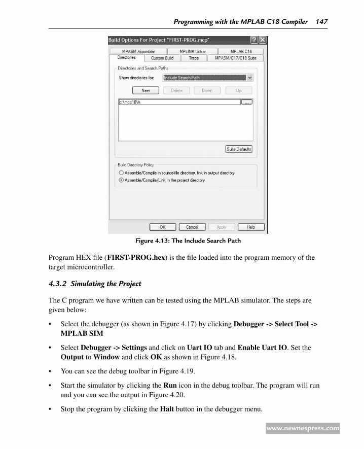
Program HEX file ( FIRST-PROG.hex) is the file loaded into the program memory of the target microcontroller.
432 simulating the Project
The C program we have written can be tested using the MPLAB simulator. The steps are given below:
Select the debugger (as shown in Figure 4.17) by clicking • Debugger -> Select Tool -> MPLAB SIM
Select • Debugger -> Settings and click on Uart IO tab and Enable Uart IO. Set the Output to Window and click OK as shown in Figure 4.18.
You can see the debug toolbar in Figure 4.19. •
Start the simulator by clicking the • Run icon in the debug toolbar. The program will run and you can see the output in Figure 4.20.
Stop the program by clicking the • Halt button in the debugger menu.
Figure 4.13: the include Search Path
Programming with the MPLAB C18 Compiler 147
www.newnespress.com
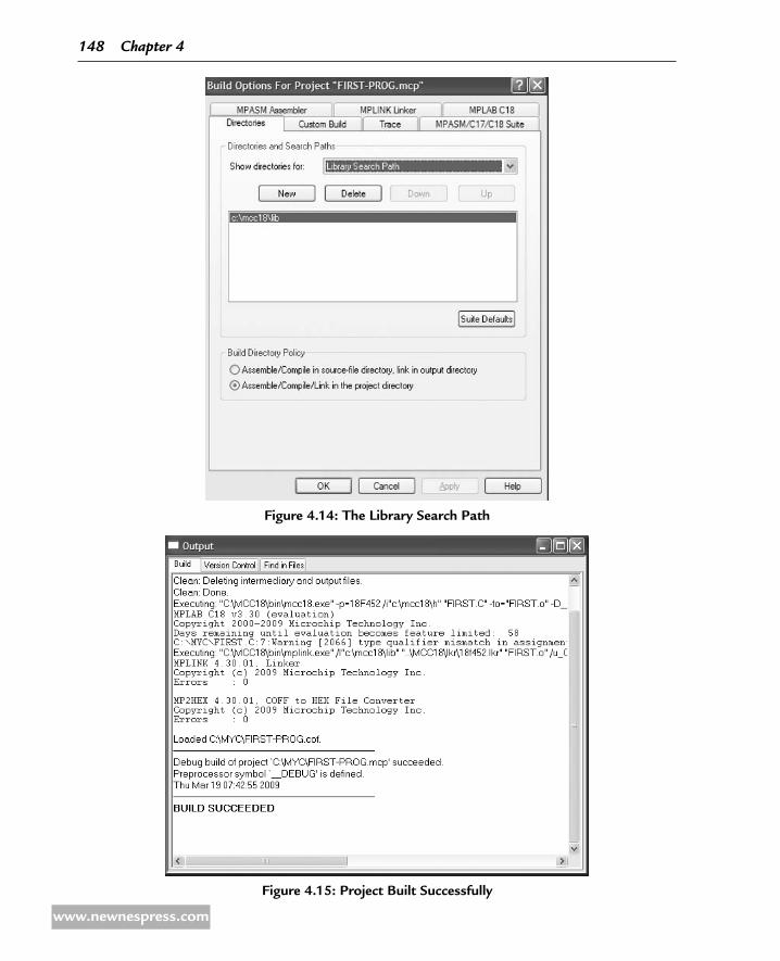
Figure 4.14: the Library Search Path
Figure 4.15: Project Built Successfully
148 Chapter 4
www.newnespress.com

Figure 4.16: Files Created in Project Folder
Figure 4.17: Select the debugger
Figure 4.18: Set the Simulator
Programming with the MPLAB C18 Compiler 149
www.newnespress.com
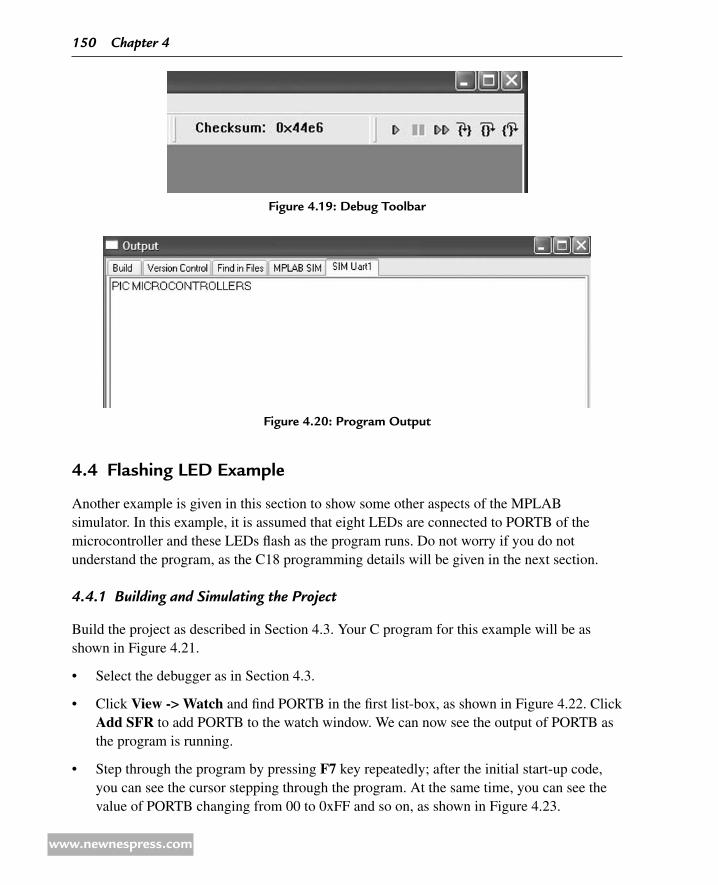
4.4 Flashing Led example
Another example is given in this section to show some other aspects of the MPLAB simulator. In this example, it is assumed that eight LEDs are connected to PORTB of the microcontroller and these LEDs flash as the program runs. Do not worry if you do not understand the program, as the C18 programming details will be given in the next section.
441 Building and simulating the Project
Build the project as described in Section 4.3. Your C program for this example will be as shown in Figure 4.21.
Select the debugger as in Section 4.3. •
Click • View -> Watch and find PORTB in the first list-box, as shown in Figure 4.22. Click Add SFR to add PORTB to the watch window. We can now see the output of PORTB as the program is running.
Step through the program by pressing • F7 key repeatedly; after the initial start-up code, you can see the cursor stepping through the program. At the same time, you can see the value of PORTB changing from 00 to 0xFF and so on, as shown in Figure 4.23.
Figure 4.19: debug toolbar
Figure 4.20: Program Output
150 Chapter 4
www.newnespress.com

Figure 4.21: the C Program of the example
Figure 4.22: Set the Watch Window
Figure 4.23: POrtB Changes in the Watch Window
Programming with the MPLAB C18 Compiler 151
www.newnespress.com

4.5 Structure of the MPLaB C18 Compiler
The basic structure of a MPLAB C18 program is shown in Figure 4.24. At the beginning of the program, we usually have comments that describe what the program is all about, the name of the program file, program version number, the author of the program, the date the program was created, and a list of modifications with dates.
Then we have the device-specific header files declared using statements like #include <p18xxxx.h>. The header file includes the names of various special function registers used in the program. We can then optionally declare the other source files to be included in our main program, using the #include statement, followed by the filenames.
The symbols used in the program can then be declared using the #define statements. The next statement is usually a compiler directive called #pragma config, which is used to select the clock source, enable/disable the watchdog timer, and set other configuration bits.
We can then define any global variable used in the program. These global variables can be accessed from any part of the main program or its functions or procedures.
The functions and procedures used in the program are then declared one after the other.
We finally have the code of the main program, starting with the statement void main (void) and then the body of the program is contained within a pair of curly brackets:
void main (void)
………….. Body of the main program…………..
The program always starts to execute from the main program.
The following sections give details of the C18 language topics.
451 Comments
Comments are used by programmers to clarify the operation of the program or a programming statement. Comment lines are ignored and are not compiled by the compiler. Two types of comments can be used in C18 programs: long comments, extending several lines, and short comments occupying only a single line. Comment lines are usually used at the beginning of a program to describe briefly the operation of the program, the name of the author, the program filename, the date the program was written, and a list of version numbers with the modifications in each version. As shown in Figure 4.24, comments can also be used after statements to describe the operations performed by the statements. A well-commented program is important for the maintenance and, thus, for the future lifetime of a program.
152 Chapter 4
www.newnespress.com

Figure 4.24: Structure of a C18 Program
/* This is a comment line which describes the program
File: Example.c Version: 1.0 Author: Dogan Ibrahim Date: March, 2009
List of Modifications:
*/
/* Include Files */#include <p18xxxxx.h>#include ……..
/* Symbol Definitions */#define MAX 100#define … ….
#pragma config WDTEN = OFF
/* Global Variables */int x,y,z,…..char a, b, c,………..
/* Function Declarations */int Func(char r) …………. …………. return …
….….
/* Start of MAIN Program */void main(void) ………….. ………….. ………….. …………..
Programming with the MPLAB C18 Compiler 153
www.newnespress.com

In general, any programmer will find it easier to modify and/or update a well-commented program.
As shown in Figure 4.24, long comments start with characters “/*” and terminate with characters “*/”. Similarly, short comments start with characters “//”; they can only occupy one line and there is no need to terminate short comments.
452 Terminating Program statements
In C language, all program statements must be terminated with the semicolon (“;”) character, otherwise a compiler error will be generated:
j = 5; // correctj = 5 // error
453 White spaces
White spaces are spaces, blanks, tabs, and new-line characters. All white spaces are ignored by the C compiler. Thus, the following three sequences are all identical:
int i; char j;
or
int i;char j;
or
int i; char j;
Similarly, the following sequences are identical:
i = j + 2;
or
i = j + 2;
454 Case sensitivity
The C language is case sensitive and variables with lowercase names are different from those with uppercase names. Thus, the following variables are all different and they represent different locations in memory:
total TOTAL Total ToTal total totaL
154 Chapter 4
www.newnespress.com

455 Variable Names
In C language, variable names can begin with an alphabetical character or with an underscore. In essence, variable names can be any of the characters a–z and A–Z, the digits 0–9, and the underscore character “_”. Each variable name should be unique within the first 31 characters of its name. Variable names can contain uppercase and lowercase characters, and numeric characters can be used inside a variable name. Examples of valid variable names are as follows:
Sum count sum100 counter il UserName _myName
Some names are reserved for the compiler itself, and they cannot be used as variable names in our programs. Some reserved names are as follows:
int char float static for while switch
long do if else struct union break
456 Variable Types
C18 language supports the variable types shown in Table 4.1. Examples of variables are given in this section.
unsigned char: These are 8-bit unsigned variables with a range 0–255. In the following example, two 8-bit variables named total and sum are created and sum is assigned a decimal value 150:
unsigned char total, sum;sum = 150;
types Size (bits) range
char 8 −128 to +127
signed char 8 −128 to +127
unsigned char 8 0 to 255
int 16 −32 768 to +32 767
unsigned int 16 0 to 65 535
short 16 −32 768 to +32 767
unsigned short 16 0 to 65 535
short long 24 −8 388 608 to +8 388 607
unsigned short long 24 0 to 16 777 215
long 32 −2 147 483 648 to +2 147 483 647
unsigned long 32 0 to 4 294 967 295
float 32 ±1.17549E-38 to ±6.80565E38
double 32 ±1.17549E-38 to ±6.80565E38
table 4.1: C18 Variable types
Programming with the MPLAB C18 Compiler 155
www.newnespress.com
Variables can be assigned values during their declaration. Thus, the above statements can also be written as:
unsigned char total, sum = 150;
char or signed char: These are 8-bit signed character variables ranging from −128 to +127. In the following example, a signed 8-bit variable named counter is created with a value of −50:
signed char counter = −50;
or,
char counter = −50;
or,
unsigned char counter;counter = −50;
int or short: These are 16-bit signed variables ranging from −32 768 to +32 767. In the following example, a signed integer named Big is created and assigned the value 32 000:
int Big = 32000;
or
short Big;Big = 32000;
unsigned int or unsigned short: These are 16-bit unsigned variables with a range 0–65 535. In the following example, an unsigned 16-bit variable named count is created and is assigned value 12 000:
unsigned int count = 12000;
or
unsigned short count = 12000;
short long: These variables are signed and 24 bits long ranging from −8 388 608 to +8 388 607. An example is given below:
short long LargeNumber;short long Big = −50000;
or
short long BigNo;BigNo = −25000;
unsigned short long: These are 24-bit unsigned variables having the range 0–16 777 215. An example is given below:
unsigned short long VeryLargeNumber;
156 Chapter 4
www.newnespress.com
long: These are 32-bit signed numbers used in arithmetic operations where large integer numbers are required. The range of long numbers is −2 147 483 648 to +2 147 483 647. In the following example, variable Count is assigned the value 2 000 250 500
long Count = 2000250500;
unsigned long: These integer numbers are 32 bits wide and unsigned. The range is 0 to +4 294 967 295. In the following example, variable Total is assigned a value 3 250 900 290.
unsigned long Total = 3250900290;
float or double: These are floating point variables implemented using Microchip AN575 32-bit format, which is IEEE 754 compliant. Floating point numbers range from ±1.17549E-38 to ±6.80565E38. In the following example, a floating point variable named area is created and is assigned a value 12.235
float area;area = 12.235;
457 Constants
Constants represent fixed values (numeric or character) in programs that cannot be changed. Con-stants are stored in the flash program memory of the PIC microcontroller; thus, the valuable and limited RAM is not wasted. In C18, constants can be integer, floating point, character, string, or enumerated types. It is important that values must be assigned to constants when they are declared.
Integer Constants
Integer constants can be decimal, hexadecimal, octal, or binary. The data type of a constant is derived by the compiler from its value. However, suffixes can be used to change the type of a constant.
From Table 4.1, we can see that integer variables can be 8, 16, 24, or 32 bit wide. In C18 language, Constants are declared using the key word const rom, and they are stored in the flash program memory of the PIC microcontroller, thus not wasting any valuable RAM space (it is important to note that in most C languages constants are declared using the key word const only). In the following example, constant integer MAX is declared as 100 and is stored in the flash program memory of the PIC microcontroller:
const rom int MAX = 100;
Hexadecimal constants start with the characters 0x and may contain numeric data 0–9 and hexadecimal characters A–F. In the following example, constant TOTAL is given the hexadecimal value FF:
const rom int TOTAL = 0xFF;
Programming with the MPLAB C18 Compiler 157
www.newnespress.com

Octal constants have a zero at the beginning of the number and may contain numeric data 0–7. In the following example, constant CNT is given an octal value 17:
const rom int CNT = 017;
Binary constant numbers start with 0b and may contain only 0 or 1. In the following example, a constant named Min is declared having the binary value “11110000”:
const rom int Min = 0b11110000
Floating Point Constants
Floating point constant numbers have integer parts, a dot, fractional part, and an optional e or E followed by a signed integer exponent. In the following example, a constant named TEMP is declared having the fractional value 37.50:
const rom TEMP = 37.50
or
const rom TEMP = 3.750E1
Character Constants
A character constant is a character enclosed in a single quote. In the following example, a constant named First_Alpha is declared having the character value “A”:
const rom char First_Alpha = 'A';
Character Array Constants
A character array consists of a number of characters stored sequentially in a variable. In the following example, a character array named Product is declared storing the characters COMPUTER:
const rom char Product[ ] = 'C', 'O', 'M', 'P', 'U', 'T', 'E', 'R';
Note that it is not necessary to declare the size of the array as this is automatically calculated by the compiler. The above statement could also be written as follows to show that the char-acter array consists of eight characters:
const rom char Product[8] = 'C', 'O', 'M', 'P', 'U', 'T', 'E', 'R';
String Constants
String constants are fixed sequences of characters stored in the flash memory of the micro-controller. The string must begin with a double quote character (“) and also terminate with a double quote character. The compiler automatically inserts a null character as a terminator. An example string constant is
const rom char x = "This is an example string constant";
158 Chapter 4
www.newnespress.com

A string constant can be extended across a line boundary using a backslash character (“\”):
const rom char x = "This is first part \ and this is second part"
The above string constant declaration is same as
const rom char x = "This is first part and this is second part"
Enumerated Constants
Enumeration constants are integer type, and they are used to make a program easier to follow. In the following example, the colors constant stores the names of colors. The first element is given the value 0 by default but it can be changed if desired:
const rom enum colors black, brown, red, orange, yellow, green, blue, gray, white;
where black is assigned 0, brown is assigned 1, red is assigned 2, and so on.
or
const rom enum days Monday = 1, Tuesday, Wednesday, Thursday, Friday, Saturday;
where Monday is assigned 1, Tuesday is assigned 2, Wednesday is assigned 3, and so on.
458 Escape sequences
Escapes sequences are used to represent nonprintable ASCII characters. Table 4.2 shows some of the commonly used escape sequences and their representation in C language. For example, the character combination “\n” represents the new-line character. An ASCII character can also be represented by specifying its hexadecimal code after a backslash. For example, the new-line character can also be represented as “\x0A.”
escape Sequences hex Values Characters
\a 0x07 BEL (bell)
\b 0x08 BS (backspace)
\t 0x09 HT (horizontal tab)
\n 0x0A LF (line feed)
\v 0x0B VT (vertical feed)
\f 0x0C FF (form feed)
\r 0x0D CR (carriage return)
\xH String of hex digits
table 4.2: Some of the Commonly Used escape Sequences
Programming with the MPLAB C18 Compiler 159
www.newnespress.com

459 static Variables
Static variables are local variables usually used in functions when it is required to preserve the last value of a variable between successive calls to the function. As shown below, static variables are declared using the key word static:
static unsigned char count;
4510 External Variables
Using the key word extern before a variable name declares that variable as external. This key word indicates to the compiler that the variable is declared elsewhere in a separate source code module. In the following example, variables sum1 and sum2 are declared as external unsigned integer:
extern int sum1, sum2;
4511 Volatile Variables
Volatile variables are important, especially in interrupt-based programs and in input–output (I/O) routines. Using the key word volatile indicates that the value of a variable may change during the lifetime of the program, independent from the normal flow of the program. Variables declared as volatile are not optimized by the compiler since their values can change at any unexpected time. In the following example, variable Led is declared as volatile unsigned char:
volatile unsigned char Led;
4512 Enumerated Variables
Enumerated variables are used to make a program more readable. In an enumerated vari-able, a list of items is specified and the value of the first item is set to 0, the next item is set to 1, and so on. In the following example, type Week is declared as an enumerated list and MON = 0, TUE = 1, WED = 2, and so on:
enum Week MON, TUE, WED, THU, FRI, SAT, SUN;
It is possible to change the values of the elements in an enumerated list. In the following example, black = 2, blue = 3, red = 4, and so on.
enum colors black = 2, blue, red, white, gray;
Similarly, in the following example, black = 2, blue = 3, red = 8, and gray = 9:
enum colors black = 2, blue, red = 8, gray;
Variables of type enumeration can be declared by specifying them after the list of items. For example, to declare variable My_Week of enumerated type Week, use the following statement:
enum Week MON, TUE, WED, THU, FRI, SAT, SUN My_Week;
160 Chapter 4
www.newnespress.com

Now, we can use variable My_Week in our programs:
My_Week = WED // assign 2 to My_Week
or
My_Week = 2 // same as above
After defining the enumeration type Week, we can declare variables This_Week and Next_Week of type Week as
enum Week This_Week, Next_Week;
4513 Arrays
Arrays are used to store related items together and sequentially in the same block of memory and under a specified name. An array is declared by specifying its type, name, and the number of elements it will store. For example,
unsigned int Total[5];
creates an array of type unsigned int, with name Total and has five elements. The first element of an array is indexed with 0. Thus, in the above example, Total[0] refers to the first element of this array and Total[4] refers to the last element. The array total is stored in memory in five consecutive locations as follows:
Total[0]
Total[1]
Total[2]
Total[3]
Total[4]
Data can be stored in the array by specifying the array name and index. For example, to store 25 in the second element of the array, we have to write
Total[1] = 25;
Similarly, the contents of an array can be read by specifying the array name and its index. For example, to copy the third array element to a variable called temp, we have to write
Temp = Total[2];
The contents of an array can be initialized during the declaration of the array by assigning a sequence of comma delimited values to the array. An example is given below where array months has 12 elements and months[0] = 31, months[1] = 28, and so on.:
unsigned char months[12] = 31,28,31,30,31,30,31,31,30,31,30,31;
Programming with the MPLAB C18 Compiler 161
www.newnespress.com

The above array can also be declared without specifying the size of the array:
unsigned char months[ ] = 31,28,31,30,31,30,31,31,30,31,30,31;
Character arrays can be declared similarly. In the following example, a character array named Hex_Letters is declared with six elements:
unsigned char Hex_Letters[ ] = 'A', 'B', 'C', 'D', 'E', 'F';
Strings are character arrays with a null terminator. Strings can either be declared by enclosing the string in double quotes or by specifying each character of the array within single quotes and can then be terminated with a null character. In the following example, the two string declarations are identical and both occupy five locations in memory:
unsigned char Mystring[ ] = "COMP";
and
unsigned char Mystring[ ] = 'C', 'O', 'M', 'P', '\0';
In C programming language, we can also declare arrays with multiple dimensions. One-dimensional arrays are usually called vectors and two-dimensional arrays are called matrices. A two-dimensional array is declared by specifying the data type of the array, array name, and the size of each dimension. In the following example, a two-dimensional array named P having three rows and four columns is created. Altogether the array has 12 elements. The first element of the array is P[0][0] and the last element is P[2][3]. The structure of this array is shown below:
Elements of a multidimensional array can be specified during the declaration of the array. In the following example, two-dimensional array Q has two rows and two columns and its diagonal elements are set to one and nondiagonal elements are cleared to zero:
unsigned char Q[2][2] = 1,0, 0,1 ;
4514 Pointers
Pointers are an important part of the C language and they hold the memory addresses of variables. Pointers are declared same as any other variables but with the character (“*”) before the variable name. In general, pointers can be created to point to (or hold the addresses of) character variables, integer variables, long variables, floating point variables, or they can point to functions.
P[0][0] P[0][1] P[0][2] P[0][3]
P[1][0] P[1][1] P[1][2] P[1][3]
P[2][0] P[2][1] P[2][2] P[2][3]
162 Chapter 4
www.newnespress.com

In the following example, an unsigned character pointer named pnt is declared:
unsigned char *pnt;
When a new pointer is created, its content is initially unspecified and it does not hold the address of any variable. We can assign the address of a variable to a pointer using the (“&”) character:
pnt = &Count;
Now pnt holds the address of variable Count. Variable Count can be set to a value using the character (“*”) before its pointer. For example, Count can be set to 10 using its pointer:
*pnt = 10; // Count = 10
which is same as
Count = 10; // Count = 10
or the value of Count can be copied to variable Cnt using its pointer:
Cnt = *pnt; // Cnt = Count
Array Pointers
In C language, the name of an array is also a pointer to the array. Thus, for the array
unsigned int Total[10];
The name Total is also a pointer to this array and it holds the address of the first element of the array. Thus, the following two statements are equal:
Total[2] = 0;
and
*( Total + 2) = 0;
Also, the following statement is true:
&Total[ j ] = Total + j
In C language, we can perform pointer arithmetic that may involve the following:
Comparing two pointers •
Adding or subtracting a pointer and an integer value •
Subtracting two pointers •
Assigning one pointer to another one •
Comparing a pointer to null •
Programming with the MPLAB C18 Compiler 163
www.newnespress.com

For example, let us assume that pointer P is set to hold the address of array element Z[2]
P = &Z[2];
We can now clear elements 2 and 3 of array Z as in the following two examples. The two examples are identical except that in the first example pointer P holds the address of Z[3] at the end of the statements and it holds the address of Z[2] at the end of the second set of statements:
*P = 0; // Z[2] = 0 P = P + 1; // P now points to element 3 of Z*P = 0; // Z[3] = 0
or*P = 0; // Z[2] = 0*( P + 1) = 0; // Z[3] = 0
A pointer can be assigned to another pointer. An example is given below where both variables Cnt and Tot are set to 10 using two different pointers:
unsigned int *i, *j; // declare 2 pointersunsigned int Cnt, Tot; // declare two variablesi = &Cnt; // i points to Cnt*i = 10; // Cnt = 10j = i; // copy pointer i to pointer jTot = *j; // Tot = 10
Incrementing Pointers
It is important to realize that when a pointer is incremented, it is scaled by the size of the object it points to. For example, if the pointer is of type long, then incrementing the pointer will increment its value by 4 since a long is 4 bytes long. An example is given below where a long array called w is declared with three elements and then each element is cleared to zero using pointers. Notice that the statement p = p + 1 increments the value of p by 4 and not by 1:
long w[5] = 1, 2, 3; // Declare array wlong p; // Declare a long pointer
p = w; // Point to array w*p = 0; // Clear first element to 0p = p + 1; // Point to next element*p = 0; // Clear second element to 0p = p + 1; // Point to next element*p = 0; // Clear third element to zero
4515 structures
Structures can be used to collect related items as single objects. Unlike arrays, the members of structures can be a mixture of any data type. For example, a structure can be created to store the personal details (name, surname, age, date of birth, etc.) of a student.
164 Chapter 4
www.newnespress.com

A structure is created using the key word struct, followed by a structure name, and a list of member declarations. Optionally, variables of the same type as the structure can be declared at the end of the structure.
The following example declares a structure named Person:
struct Person
unsigned char name[20];unsigned char surname[20];unsigned char nationality[20];unsigned char age;
Declaring a structure does not occupy any space in memory, but the compiler creates a template describing the names and types of the data objects or member elements that will eventually be stored within such a structure variable. It is only when variables of the same type as the structure are created, then these variables occupy space in memory. We can declare variables of the same type as the structure by giving the name of the structure and the name of the variable. For example, two variables Me and You of type Person can be created by the statement:
struct Person Me, You;
Variables of type Person can also be created during the declaration of the structure as shown below:
struct Person
unsigned char name[20];unsigned char surname[20];unsigned char nationality[20];unsigned char age;
Me, You;
We can assign values to members of a structure by specifying the name of the structure, fol-lowed by a dot (“.”), and the name of the member. In the following example, the age of structure variable Me is set to 25 and variable M is assigned to the value of age in structure variable You.
Me.age = 25;M = You.age;
Structure members can be initialized during the declaration of the structure. In the following example, the radius and height of structure Cylinder are initialized to 1.2 and 2.5, respectively.
struct Cylinder
float radius;float height;
MyCylinder = 1.2, 2.5;
Programming with the MPLAB C18 Compiler 165
www.newnespress.com

Values can also be set to members of a structure using pointers by defining the variable types as pointers. For example, if TheCylinder is defined as a pointer to structure Cylinder, then we can write
struct Cylinder
float radius;float height;
*TheCylinder;
TheCylinder -> radius = 1.2;TheCylinder -> height = 2.5;
The size of a structure is the number of bytes contained within the structure. We can use the sizeof operator to get the size of a structure. Considering the above example,
sizeof(MyCylinder)
returns 8, since each float variable occupies 4 bytes in memory.
Bit fields can be defined using structures. With bit fields, we can assign identifiers to bits of a variable. For example, to identify bits 0, 1, 2, and 3 of a variable as LowNibble and to identify the remaining 4 bits as HighNibble, we can write
struct
LowNibble: 4;HighNibble: 4;
MyVariable;
We can then access the nibbles of variable MyVariable as
MyVariable.LowNibble = 12;MyVariable.HighNibble = 8;
In C language, we can use the typedef statements to create new types of variables. For example, a new structure data type named Reg can be created as follows:
typedef struct
unsigned char name[20];unsigned char surname[20];unsigned age;
Reg;
Variables of type Reg can then be created in exactly the same way as creating any other types of variables. In the following example, variables MyReg, Reg1, and Reg2 are created from data type Reg:
Reg MyReg, Reg1, Reg2;
166 Chapter 4
www.newnespress.com

The contents of one structure can be copied to another structure provided that both structures have been derived from the same template. In the following example, two structure variables P1 and P2 of same type have been created and P2 is copied to P1:
struct Person
unsigned char name[20];unsigned char surname[20];unsigned int age;unsigned int height;unsigned weight;
struct Person P1, P2;…………………………………………P2 = P1;
4516 Unions
Unions are used to overlay variables. A union is similar to a structure, and it is even defined in a similar manner; both are based on templates and their members are accessed using the “.” or “->” operators. The difference of a union is that all variables in a union occupy the same memory area. In other words, all member elements of a union share the same common stor-age. An example for union declaration is given below:
union flags
unsigned char x;unsigned int y;
P;
In this example, variables x and y occupy the same memory area, and the size of this union is 2 bytes long, which is the size of the biggest member of the union. When variable y is loaded with a 2-byte value, variable x will have the same value as the low byte of y. In the following example, y is loaded with 16-bit hexadecimal value 0xAEFA and x is loaded with 0xFA:
P.y = 0xAEFA;
The size of a union is the size (number of bytes) of its largest member. Thus, the statement
sizeof(P)
returns 2.
Programming with the MPLAB C18 Compiler 167
www.newnespress.com

The above union could also have been declared as
union flags
unsigned char x;unsigned int y;
union flags P;
4517 Operators in C
Operators are applied to variables and other objects in expressions, and they cause some con-ditions or some computations to occur.
C18 language supports the following operators:
Arithmetic operators •
Logical operators •
Bitwise operators •
Conditional operators •
Assignment operators •
Relational operators •
Preprocessor operators •
Arithmetic Operators
Arithmetic operators are used in arithmetic computations. Arithmetic operators associate from left to right, and they return numerical results. A list of the C18 arithmetic operators is given in Table 4.3.
Operators Operations
+ Addition
− Subtraction
* Multiplication
/ Division
% Remainder (integer division)
+ + Autoincrement
− − Autodecrement
table 4.3: C18 arithmetic Operators
168 Chapter 4
www.newnespress.com

Example for use of arithmetic operators is given below:
/* Adding two integers */5 + 12 // equals 17
/* Subtracting two integers */120 − 5 // equals 11510 − 15 // equals −5
/* Dividing two integers */5 / 3 // equals 112 / 3 // equals 4
/* Multiplying two integers */3 * 12 // equals 36
/* Adding two floating point numbers */3.1 + 2.4 // equals 5.5
/* Multiplying two floating point numbers */2.5 * 5.0 // equals 12.5
/* Dividing two floating point numbers */25.0 / 4.0 // equals 6.25
/* Remainder (not for float) */7 % 3 // equals 1
/* Post-increment operator */j = 4;k = j++; // k = 4, j = 5
/* Pre-increment operator */j = 4;k = ++j; // k = 5, j = 5
/* Post-decrement operator */j = 12;k = j−−; // k = 12, j = 11
/* Pre-decrement operator */j = 12;k = −−j; // k = 11, j = 11
Relational Operators
Relational operators are used in comparisons. If the expression evaluates to TRUE, 1 is returned otherwise 0 is returned.
Programming with the MPLAB C18 Compiler 169
www.newnespress.com

All relational operators associate from left to right, and a list of mikroC relational operators is given in Table 4.4.
Example for use of relational operators is given below:
x = 10x > 8 // returns 1x = = 10 // returns 1x < 100 // returns 1x > 20 // returns 0x != 10 // returns 0x >= 10 // returns 1x <= 10 // returns 1
Logical Operators
Logical operators are used in logical and arithmetic comparisons, and they return TRUE (i.e., logical 1) if the expression evaluates to nonzero or FALSE (i.e., logical 0) if the expression evaluates to zero. If more than one logical operator is used in a statement and if the first con-dition evaluates to false, the second expression is not evaluated.
A list of the C18 logical operators is given in Table 4.5.
Example for use of logical operators is given below:
x = 7;
x > 0 && x < 10 // returns 1x > 0 || x < 10 // returns 1
Operators Operations
= = Equal to
! = Not equal to
> Greater than
< Less than
> = Greater than or equal to
< = Less than or equal to
table 4.4: C18 relational Operators
Operators Operations
&& AND
|| OR
! NOT
table 4.5: C18 Logical Operators
170 Chapter 4
www.newnespress.com

x >=0 && x <=10 // return 1x >=0 && x < 5 // returns 0
a = 10; b = 20; c = 30; d = 40;
a > b && c > d // returns 0b > a && d > c // returns 1a > b || d > c // returns 1
Bitwise Operators
Bitwise operators are used to modify the bits of a variable. A list of the C18 bitwise operators is given in Table 4.6.
Bitwise AND returns 1 if both bits are 1, else it returns 0.
Bitwise OR returns 0 if both bits are 0, otherwise it returns 1.
Bitwise XOR returns 1 if both bits are complementary, otherwise it returns 0.
Bitwise complement inverts each bit.
Bitwise shift left and shift right move the bits to the left or right, respectively.
Example for use of bitwise operators is given below:
i. 0xFA & 0xEE returns 0xEA
0xFA: 1111 1010 0xEE: 1110 1110 --------------------- 0xEA: 1110 1010
ii. 0x01 | 0xFE returns 0xFF
0x08: 0000 0001 0xFE: 1111 1110 --------------------- 0xFE: 1111 1111
Operators Operations
& Bitwise AND
| Bitwise OR
^ Bitwise EXOR
~ Bitwise complement
<< Shift left
>> Shift right
table 4.6: C18 bitwise operators
Programming with the MPLAB C18 Compiler 171
www.newnespress.com

iii. 0xAA ^ 0x1F returns 0xB5
0xAA: 1010 1010 0x1F : 0001 1111 --------------------- 0xB5: 1011 0101
iv. ~0xAA returns 0x55
0xAA: 1010 1010 ~ : 0101 0101 -------------------- 0x55: 0101 0101
v. 0x14 >> 1 returns 0x08 (shift 0x14 right by 1 digit)
0x14: 0001 0100 >>1 : 0000 1010 --------------------- 0x0A: 0000 1010
vi. 0x14 >> 2 returns 0x05 (shift 0x14 right by 2 digits)
0x14: 0001 0100 >> 2: 0000 0101 --------------------- 0x05: 0000 0101
vii. 0x235A << 1 returns 0x46B4 (shift left 0x235A left by 1 digit)
0x235A: 0010 0011 0101 1010 <<1 : 0100 0110 1011 0100 -------------------------------------- 0x46B4 : 0100 0110 1011 0100
viii. 0x1A << 3 returns 0xD0 (shift left 0x1A by 3 digits)
0x1A: 0001 1010 <<3 : 1101 0000 --------------------- 0xD0: 1101 0000
Assignment Operators
In C language, there are two types of assignments: simple assignments and compound assign-ments. In simple assignments, an expression is simply assigned to another expression or an operation is performed using an expression and the result is assigned to another expression:
Expression1 = Expression2
orResult = Expression1 operation Expression2
172 Chapter 4
www.newnespress.com
Examples of simple assignments are
Temp = 10;Cnt = Cnt + Temp;
Compound assignments have the general format:
Result operation = Expression1
Here, the specified operation is performed on Expression1 and the result is stored in Result. For example,
j + = k; is same as j = j + k;
also,p * = m; is same as p = p * m;
The following compound operators can be used in C18 programs:
+ = − = * = /= % =
& = | = ^ = >> = << =
Conditional Operator
The syntax of the conditional operator is
Result = Expression1 ? Expression2: Expression3
Expression1 is evaluated first and if its value is true, Expression2 is assigned to Result, other-wise Expression3 is assigned to Result. In the following example, maximum of x and y is found, where x is compared with y, and if x > y, then max = x, otherwise max = y
max = (x > y) ? x:y;
In the following example, lowercase characters are converted to uppercase. If the character is lowercase (between “a” and “z”), then by subtracting 32 from the character, we obtain the equivalent uppercase character:
c = (c> = ‘a’&& c< = ‘z’) ? (c−32):c;
Preprocessor Operators
The preprocessor allows a programmer to
Compile a program conditionally such that parts of the code are not compiled •
Replace symbols with other symbols or values •
Insert text files into a program •
Programming with the MPLAB C18 Compiler 173
www.newnespress.com

The preprocessor operator is the (“#”) character, and any line of code with a leading (“#”) is assumed to be a preprocessor command. Semicolon character (“;”) is not needed to terminate a preprocessor command.
C compiler supports the following preprocessor commands:
#define #undef#if #elif #endif#ifdef #ifndef#error#line#pragma
#define, #undef, #ifdef, #ifndef
#define preprocessor command provides Macro expansion where every occurrence of an identifier in the program is replaced with the value of the identifier. For example, to replace every occurrence of MAX with value 100, we can write
#define MAX 100
An identifier that has already been defined cannot be defined again unless both defi-nitions have the same values. One way to get round this problem is to remove the Macro definition:
#undef MAX
or the existence of a Macro definition can be checked. In the following example, if MAX has not already been defined, then it is given value 100, otherwise the #define line is skipped:
#ifndef MAX#define MAX 100
#endif
Note that the #define preprocessor command does not occupy any space in memory.
We can pass parameters to a Macro definition by specifying the parameters in parenthesis after the Macro name. For example, consider the Macro definition
#define ADD(a, b) (a + b)
When this Macro is used in a program, (a,b) will be replaced with (a + b) as shown below:
p = ADD(x, y) will be transformed into p = (x + y)
Similarly, we can define a Macro to calculate the square of two numbers:
#define SQUARE(a) (a * a)
174 Chapter 4
www.newnespress.com

When we now use this Macro in a program,
p = SQUARE(x) will be transformed into p = (x * x)
#include
The preprocessor directive #include is used to include a source file in our program. Usually, header files with extension “.h” are used with #include. There are two formats for using the #include:
#include <file>
and#include "file"
In the first option, the file is searched in the C18 installation directory first and then in the user search paths. In the second option, the specified file is searched in the C18 project folder, then in the C18 installation folder, and then in the user search paths. It is also possible to specify a complete directory path as
#include "C:\temp\last.h"
The file is then searched only in the specified directory path.
#if, #elif, #else, #endif
The above preprocessor commands are used for conditional compilation where parts of the source code can be compiled only if certain conditions are met. In the following example, the code section where variables A and B are cleared to zero is compiled if M has a nonzero value, otherwise the code section where A and B are both set to 1 is compiled. Notice that the #if must be terminated with #endif:
#if MA = 0;B = 0;
#elseA = 1;B = 1;
#endif
We can also use the #elif condition that tests for a new condition if the earlier condition was false:
#if MA = 0;B = 0;
#elif NA = 1;B = 1;
Programming with the MPLAB C18 Compiler 175
www.newnespress.com
#elseA = 2;B = 2;
#endif
In the above example, if M has a nonzero value code section, then A = 0; B = 0; is com-piled. If N has a nonzero value, then code section A = 1; B = 1; is compiled. Finally, if both M and N are zero, then code section A = 2; B = 2; is compiled. Notice that only one code section is compiled between #if and #endif and a code section can contain any number of statements.
#pragma
The #pragma directive is used to define device-specific constructs. This directive is used with the key words as shown below:
#pragma code •
#pragma romdata •
#pragma idata •
#pragma config •
#pragma interrupt •
#pragma interruptflow •
#pragma varlocate •
#pragma code is used to instruct the compiler to compile all subsequent instructions into the program memory section of the target processor.
#pragma romdata is used to instruct the compiler to compile the subsequent static data into the program memory of the target processor.
#pragma udata is used to locate the uninitialized user variables in data memory.
#pragma idata is used to locate the initialized user variables in data memory.
#pragma interrupt is used to instruct the compiler to compile the code from the named C function as a high-priority interrupt service routine.
#pragma interruptflow is used to instruct the compiler to compile the named C function as a low-priority interrupt service routine.
#pragma varlocate is used to specify where the variables will be located so that the compiler will not generate extraneous instructions to set the bank when accessing the variables.
176 Chapter 4
www.newnespress.com

#pragma config is used to define the processor Configuration bits. Document “PIC18 Configuration Settings Addendum” of Microchip Inc. gives tables of all the configuration bits available for any member of the PIC18 family. Some of the widely used configuration bit definitions for the popular PIC18F452 microcontroller are shown in Table 4.7. As an example, to disable the watchdog and set the oscillator to XT type crystal operation, we can use the following statement:
#pragma config WDT = OFF#pragma config OSC = XT
It is permissible to combine the various settings on a single line, i.e.,
#pragma config WDT = OFF, OSC = XT
Oscillator Selection
OSC = LP LP
OSC = XT XT
OSC = HS HS
OSC = RC RC
OSC = EC EC and OSC2 as clock out
OSC = ECIO EC and OSC2 as port RA6
OSC = HSPLL HS–PLL enabled
OSC = RCIO RC and OSC2 as port RA6
Power-up timer
PWRT = ON Timer enabled
PWRT = OFF Timer disabled
Watchdog timer
WDT = OFF Watchdog disabled
WDT = ON Watchdog enabled
Watchdog Postscaler
WDTPS = 1 1:1
WDTPS = 2 1:2
WDTPS = 4 1:4
WDTPS = 8 1:8
WDTPS = 16 1:16
WDTPS = 32 1:32
WDTPS = 64 1:64
WDTPS = 128 1:128
table 4.7: Widely Used PiC18F452 Microcontroller Configuration Bits
Programming with the MPLAB C18 Compiler 177
www.newnespress.com

4518 Modifying the Flow of Control
Statements are normally executed sequentially from the beginning to the end of a program. We can use control statements to modify the normal sequential flow of control in a C pro-gram. The following control statements are available in C18 programs:
Selection statements •
Unconditional modification of flow •
Iteration statements •
Selection Statements
There are two selection statements: If and switch.
if Statement
The general format of the if statement is
if(expression)Statement1;
elseStatement2;
or,
if(expression)Statement1; else Statement2;
If the expression evaluates to TRUE, Statement1 is executed, otherwise Statement2 is executed. The else key word is optional and may be omitted if not required. In the following example, if the value of x is greater than MAX, then variable P is incremented by 1, otherwise it is decremented by 1:
if(x > MAX)P++;
elseP−−;
We can have more than one statement by enclosing the statements within curly brackets. For example,
if(x > MAX)
P++;Cnt = P;Sum = Sum + Cnt;
else
P−−;
In the above example, if x is greater than MAX, then the three statements within the curly brackets are executed, otherwise the statement P−− is executed.
178 Chapter 4
www.newnespress.com

Another example using the if statement is given below:
if(x > 0 && x < 10)
Total += Sum;Sum++;
else
Total = 0;Sum = 0;
switch Statement
The switch statement is used when there are a number of conditions, and different operations are performed when a condition is true. The syntax of the switch statement is
switch (condition)
case condition1:Statements;break;
case condition2:Statements;break;
……………………………………case conditionn:
Statements;break;
default:Statements;
The switch statement functions as follows: First, the condition is evaluated. The condition is then compared to condition1, and if a match is found, statements in that case block are evaluated and control jumps outside the switch statement when the break key word is encountered. If a match is not found, condition is compared to condition2, and if a match is found, statements in that case block are evaluated and control jumps outside the switch state-ments and so on. The default is optional and statements following default are evaluated if the condition does not match to any of the conditions specified after the case key words.
In the following example, the value of variable Cnt is evaluated. If Cnt = 1, A is set to 1, if Cnt = 10, B is set to 1, and if Cnt = 100, C is set to 1. If Cnt is not equal to 1, 10, or 100, then D is set to 1:
switch (Cnt)
Programming with the MPLAB C18 Compiler 179
www.newnespress.com

case 1:A = 1;break;
case 10:B = 1;break;
case 100:C = 1;break;
default:D = 1;
Because white spaces are ignored in C language, we could also write the above code as
switch (Cnt)
case 1: A = 1; break;case 10: B = 1; break;case 100: C = 1; break;default: D = 1;
example 4.1
In an experiment, the relationship between X and Y values are found to be
Write a switch statement that will return the Y value, given the X value.
solution
The required switch statement is
switch ( X )
case 1:Y = 3.2;break;
case 2:Y = 2.5;
X Y
1 3.2
2 2.5
3 8.9
4 1.2
5 12.9
180 Chapter 4
www.newnespress.com

break;case 3:
Y = 8.9;break;
case 4:Y = 1.2;break;
case 5:Y = 12.9;
4519 Iteration statements
Iteration statements enable us to perform loops in our programs, where part of a code is repeated required number of times. In C18 language, there are four ways that iteration can be performed, and we will look at each one with examples:
Using • for statement
Using • while statement
Using • do statement
Using • goto statement
for StatementThe syntax of the for statement is
for(initial expression; condition expression; increment expression)
Statements;
The initial expression sets the starting variable of the loop, and this variable is compared against the condition expression before an entry to the loop. Statements inside the loop are executed repeatedly, and after each iteration, the value of increment expression is incre-mented. The iteration continues until the condition expression becomes false. An endless loop is formed if the condition expression is always true.
The following example shows how a loop can be set up to execute 10 times. In this example, vari-able i starts from 0 and increments by 1 at the end of each iteration. The loop terminates when i = 10 in which case the condition i < 10 becomes false. On exit from the loop, the value of i is 10:
for(i = 0; i < 10; i ++)
statements;
Programming with the MPLAB C18 Compiler 181
www.newnespress.com
The above loop could also be formed by starting the initial expression with a nonzero value. Here, i starts with 1 and the loop terminates when i = 11. Thus, on exit from the loop, the value of i is 11:
for(i = 1; i <= 10; i++)
Statements;
The parameters of a for loop are all optional and can be omitted. If the condition expression is left out, it is assumed to be true. In the following example, an endless loop is formed where the condition expression is always true and the value of i starts with 0 and is incremented after each iteration:
/* Endless loop with incrementing i */for(i = 0; ; i++)
Statements;
Another example of an endless loop is given below where all the parameters are omitted:
/* Example of endless loop */for(; ;)
Statements;
In the following endless loop, i starts with 1 and is not incremented inside the loop:
/* Endless loop with i = 1 */for(i = 1; ;)
Statements;
If there is only one statement inside the for loop, we can omit the curly brackets as shown in the following example:
for(k = 0; k < 10; k++)Total = Total + Sum;
Nested for loops can be used in programs. In a nested for loop, the inner loop is executed for each iteration of the outer loop. An example is given below where the inner loop is executed five times and the outer loop is executed 10 times. The total iteration count is 50:
/* Example of nested for loops */for(i = 0; i < 10; i++)
for( j = 0; j < 5; j++)
182 Chapter 4
www.newnespress.com

Statements;
In the following example, the sum of all the elements of a 3 × 4 matrix M is calculated and stored in a variable called Sum:
/* Add all elements of a 3x4 matrix */Sum = 0;for(i = 0; i < 3; i++)
for( j = 0; j < 4; j++)
Sum = Sum + M[i][ j ];
Because there is only one statement to be executed, the above example could also be written as
/* Add all elements of a 3x4 matrix */Sum = 0;for(i = 0; i < 3; i++)
for( j = 0; j < 4; j++) Sum = Sum + M[i][ j ];
while Statement
This is another statement that can be used to create iteration in programs. The syntax of the while statement is
while (condition)
Statements;
Here, the statements are executed repeatedly until the condition becomes false or the statements are executed repeatedly as long as the condition is true. If the condition is false on entry into the loop, then the loop will not be executed and the program will continue from the end of the while loop. It is important that the condition is changed inside the loop; otherwise an endless loop will be formed.
The following code shows how to set up a loop to execute 10 times using the while statement:
/* A loop that executes 10 times */k = 0;while (k < 10)
Programming with the MPLAB C18 Compiler 183
www.newnespress.com

Statements;k++;
At the beginning of the code, variable k is 0. Because k is less than 10, the while loop starts. Inside the loop, the value of k is incremented by 1 after each iteration. The loop repeats as long as k < 10 and is terminated when k = 10. At the end of the loop, the value of k is 10.
Notice that an endless loop will be formed if k is not incremented inside the loop:
/* An endless loop */k = 0;while (k < 10)
Statements;
An endless loop can also be formed by setting the condition to be always true:
/* An endless loop */while (k = k)
Statements;
Here is an example of calculating the sum of numbers from 1 to 10 and storing the result in variable called sum:
/* Calculate the sum of numbers from 1 to 10 */unsigned int k, sum;k = 1;sum = 0;while(k <= 10)
sum = sum + k;k++;
It is possible to have a while statement with no body. Such a statement is useful, for example, if we are waiting for an input port to change its value. An example is given below where the program will wait as long as bit 0 of PORTB (RB0) is at logic 0. The program will continue when the port pin changes to logic 1:
while(PORTBbits.RB0 == 0); // Wait until RB0 becomes 1
or
while(PORTBbits.RB0);
It is possible to have nested while statements.
184 Chapter 4
www.newnespress.com
As we shall see later, the bits of a port can be accessed using the key word bits after the port name, followed by the port bit name to be accessed.
do Statement
The do statement is similar to the while statement, but here, the loop executes until the condition becomes false or the loop executes as long as the condition is true. The condition is tested at the end of the loop. The syntax of the do statement is
do
Statements; while (condition);
The first iteration is always performed whether the condition is true or false, and this is the main difference between the while statement and the do statement.
The following code shows how to setup a loop to execute 10 times using the do statement:
/* Execute 10 times */k = 0;do
Statements;k++;
while (k < 10);
The loop starts with k = 0, and the value of k is incremented inside the loop after each iter-ation. k is tested at the end of the loop, and if k is not less than 10, the loop terminates. In this example, because k = 0 at the beginning of the loop, the value of k is 10 at the end of the loop.
An endless loop will be formed if the condition is not modified inside the loop as shown in the following example. Here, k is always less than 10:
/* An endless loop */k = 0;do
Statements; while (k < 10);
An endless loop can also be created if the condition is set to be true all the time:
/* An endless loop */do
Statements; while (k = k);
It is possible to have nested do statements.
Programming with the MPLAB C18 Compiler 185
www.newnespress.com

goto Statement
The goto statement can be used to alter the normal flow of control in a program. This state-ment causes the program to jump to a specified label. A label can be any alphanumeric character set starting with a letter and terminating with the colon (“:”) character.
Although not recommended, the goto statement can be used together with the if statement to create iterations in a program. The following example shows how to setup a loop to execute 10 times using the goto and if statements:
/* Execute 10 times *//k = 0;
Loop:/Statements;/k++;/if(k < 10)goto Loop;
The loop starts with label Loop and variable k = 0 at the beginning of the loop. Inside the loop, the statements are executed and k is incremented by 1. The value of k is then compared with 10 and the program jumps back to label Loop if k < 10. Thus, the loop is executed 10 times until the condition at the end becomes false. At the end of the loop, the value of k is 10.
continue and break Statements
The continue and break statements can be used inside iterations to modify the flow of con-trol. The continue statement is usually used with if statement and causes the loop to skip an iteration. An example is given below, which calculates the sum of numbers from 1 to 10 except number 5:
/* Calculate sum of numbers 1,2,3,4,6,7,8,9,10 */Sum = 0;i = 1;for(i = 1; i <= 10; i++)
if(i == 5) continue; // Skip number 5Sum = Sum + i;
Similarly, the break statement can be used to terminate a loop from inside the loop. In the following example, the sum of numbers from 1 to 5 are calculated even though the loop parameters are set to iterate 10 times:
/* Calculate sum of numbers 1,2,3,4,5 */Sum = 0;i = 1;for(i = 1; i <= 10; i++)
186 Chapter 4
www.newnespress.com

if(i > 5) break; // Stop loop if i > 5Sum = Sum + i;
4520 Mixing C18 with Assembly Language statements
It sometimes becomes necessary to mix PIC microcontroller assembly language statements with the C18 language statements in a program. For example, very accurate program delays can be generated using assembly language statements. Use of the assembly language is beyond the scope of this book, but the techniques for including assembly language instructions in C18 programs will be discussed in this section for those readers who are familiar with using the PIC microcontroller assembly languages.
Assembly language instructions can be included in a C18 program by starting the code, using the key word _asm and terminating with _endasm. This process is known as inline assembly and it differs from full assembly (e.g., using MPASM assembler) as follows:
Comments must be in C18 format •
Directives are not allowed •
All operands must be specified (no defaults allowed) •
Literals are specified using C radix notation (e.g., 0x12 and not H12) •
Default radix is decimal •
Indexed addressing (e.g., [ ]) is not supported •
Labels must end with a colon •
An example inline assembly program is given below:
_asm/* This assembly code introduces delay to the program*/MOVLW 6 // Load W with 6…………..…………..
done:…………..…………..GOTO done
_endasm
User declared C variables can be used in assembly language routines. For example, C variable Temp can be initialized and then loaded to the W register as
unsigned char Temp = 10;_asm
Programming with the MPLAB C18 Compiler 187
www.newnespress.com

MOVLW Temp // W = Temp = 10……………….……………….
_endasm
Global symbols, such as the predefined port names and register names, can be used in assembly language routines without having to initialize them:
_asmMOVWF PORTB, 1………………….………………….
_endasm
4.6 PiC Microcontroller i/O Port Programming
Depending on the type of microcontroller used, PIC microcontroller I/O ports are named as PORTA, PORTB, PORTC, and so on. Port pins can be in analog or digital mode. In analog mode, ports are input only and a built-in analog to digital converter and multiplexer circuits are used. In digital mode, a port pin can be configured as either input or output. The TRIS registers control the port directions and there are TRIS registers for each port, namely TRISA, TRISB, TRISC, and so on. Clearing a TRIS register bit to 0 sets the corresponding port bit to output mode. Similarly, setting a TRIS register bit to 1 sets the corresponding port bit to input mode.
Ports can be accessed either as a single 8-bit register or as individual bits. In the following example, PORTB is configured as an output port and all its bits are set to 1:
TRISB = 0; // Set PORT B as outputPORTB = 0xFF; // Set PORTB bits to 1
Similarly, the following example shows how four upper bits of PORTC can be set as input and how upper 4 bits of PORTC can be set as output:
TRISC = 0xF0;
Bits of an I/O port can be accessed using the key word bits and then specifying the required port bit name. In the following example, variable P2 is loaded with bit 2 of PORTB:
P2 = PORTBbits.RB2;
All the bits of a port can be complemented by the statement:
PORTB = ~PORTB;
188 Chapter 4
www.newnespress.com
4.7 Programming examples
In this section, some simple programming examples are given to make the reader familiar with programming in C18 language. In all the following examples, the processor header file must be included at the beginning of the program (e.g., #include <p18f452.h>)
example 4.2
Write a program to set all eight port pins of PORTB to logic 1.
solution
The required program is given below. PORTB is configured as an output port and then all port pins are set to logic 1 by sending hexadecimal number 0xFF:
void main(void)
TRISB = 0; // Configure PORT B as outputPORTB = 0xFF; // Set all port pins to logic 1
example 4.3
Write a program to set the odd numbered (bits 1, 3, 5, and 7) PORTB pins to logic 1.
solution
Odd numbered port pins can be set to logic 1 by sending the bit pattern “10101010” to the port. This bit pattern is the hexadecimal number 0xAA and the required program is
void main(void)
TRISB = 0; // Configure PORTB as outputPORTB = 0xAA; // Turn on odd numbered port pins
example 4.4
It is required to write a program to continuously count up in binary and send this data to PORTB. Thus, PORTB is required to have the binary data:
Programming with the MPLAB C18 Compiler 189
www.newnespress.com
solution
A for loop can be used to create an endless loop, and inside this loop, the value of a variable can be incremented and then sent to PORTB. The required program is:
void main(void)
unsigned char Cnt = 0;
for(;;) //Endless loop
PORTB = Cnt; // Send Cnt to PORT BCnt++; // Increment Cnt
example 4.5
Write a program to set all bits of PORTB to logic 1 and then to logic 0. Repeat this process 10 times.
solution
The for statement can be used to create a loop and repeat the required operation 10 times:
void main(void)
unsigned char j;
for( j = 0; j < 10; j++) // Repeat 10 times
PORTB = 0xFF; // Set PORT B pins to 1PORTB = 0; // Clear PORT B pins
00000000
00000001
00000010
00000011
…………...
…………...
11111110
11111111
00000000
…………...
190 Chapter 4
www.newnespress.com

example 4.6
The radius and height of a cylinder are 2.5 and 10 cm, respectively. Write a program to calculate the volume of this cylinder.
solution
The required program is
void main(void)
float Radius = 2.5, Height = 10;float Volume;
Volume = PI *Radius*Radius*Height;
example 4.7
Write a program to find the largest element of an integer array having 10 elements.
solution
The program is given below. At the beginning, variable m is set to the first element of the array. A loop is then formed and the largest element of the array is found:
void main (void)
unsigned char j;int m, A[10];
m = A[0]; //First element of arrayfor( j = 1; j < 10; j++)
if(A[ j ] > m)m = A[ j ];
example 4.8
Write a program using the while statement to clear all 10 elements of an integer array M.
Programming with the MPLAB C18 Compiler 191
www.newnespress.com

solution
As shown in the program listing below, NUM is defined to be 10 and variable j is used as the loop counter:
#define NUM 10void main(void)
int M[NUM];unsigned char j = 0;
while ( j < NUM)
M[ j ] = 0;j++;
example 4.9
Write a program to convert the temperature from °C to °F starting from 0°C, in steps of 1°C up to and including 100°C, and store the results in an array called F.
solution
Given the temperature in °C, the equivalent in °F is calculated using the formula:
F = (C − 32.0)/1.8
The required program listing is given below. A for loop is used to calculate the tempera-ture in °F and store in array F:
void main(void)
float F[100];unsigned char C;
for (C =0; C <= 100; C++)
F[C] = (C − 32.0) / 1.8;
192 Chapter 4
www.newnespress.com

4.8 Functions
A function is a self-contained section of code written to perform a well-defined action. Func-tions are usually created when it is required to perform an operation at several different parts of a main program. In addition, it is a good programming practice to divide a large program into a number of smaller independent functions. The statements within a function may be executed by calling (or invoking) the function.
The syntax of a general function definition is as shown in Figure 4.25. The data type indicates the type of data returned by the function. This is followed by the name of the function, and then a set of brackets are used where any comma separated arguments can be declared inside the brackets. Then the body of the function that includes the operational code of the function is written inside a set of opening and closing curly brackets.
An example of function definition is shown below. This function, named Mult, receives two integer arguments a and b and returns their product. Note that the use of brackets in a return statement is optional:
int Mult(int a, int b)
return (a*b);
When a function is called, it generally expects to be given the number of arguments expressed in the function’s argument list. For example, the above function can be called as
z = Mult(x,y);
where variable z has the data type int. Note that the arguments declared in the function header and the arguments passed when the function is called are independent of each other, even if they may have the same name. In the above example, when the function is called, variable x is copied to a and variable y is copied to b on entry to function Mult.
Some functions do not return any data and the data type of such functions must be declared as void. An example is given below:
void LED(unsigned char D)
PORTB = D;
type name (parameter1, parameter2,…..)
…………. function body ………….
Figure 4.25: General Syntax of a Function definition
Programming with the MPLAB C18 Compiler 193
www.newnespress.com

void functions can be called without any assignment statements, but the brackets must be used to tell the compiler that a function call is made:
LED( );
Also, some functions do not have any arguments. In the following example, the function, named Compl, complements PORTC of the microcontroller and it returns no data and has no arguments:
void Compl( )
PORTC = ~PORTC;
The above function can be called as
Compl( );
Functions are normally defined before the start of the main program.
Some example function definitions and their usage in main programs are illustrated in the following examples.
example 4.10
Write a function called Circle_area to calculate the area of a circle where the radius is to be used as an argument. Use this function in a main program to calculate the area of a circle whose radius is 2.5 cm. Store the area in a variable called Circ.
solution
The required function definition is given below. The data type of the function is declared as float. The area is calculated by the formula:
Area = r2,
where r is the radius of the circle. The area is calculated and stored in a local variable called s, which is then returned from the function:
float Circle_Area(float radius)
float s;
s = PI * radius * radius;return s;
194 Chapter 4
www.newnespress.com

Figure 4.26 shows how function Circle_Area can be used in a main program to calculate the area of a circle whose radius is 2.5 cm. The function is defined before the main program. Inside the main program, the function is called to calculate and store the area in variable Circ.
example 4.11
Write a function called area and a function called Volume to calculate the area and volume of a cylinder, respectively. Then, write a main program to calculate the area and the volume of cylinder whose radius is 2.0 cm and height is 5.0 cm. Store the area in variable cyl_area and the volume in variable cyl_volume.
solution
The area of a cylinder is calculated by the formula:
Area = 2rh,
where r and h are the radius and the height of the cylinder, respectively. Similarly, the volume of a cylinder is given by the formula:
Volume = r2h
Figure 4.27 gives the listing of the functions that calculate the area and volume of a cylinder.
The main program that calculates the area and volume of a cylinder whose radius = 2.0 cm and height = 5.0 cm is shown in Figure 4.28.
example 4.12
Write a function called LowertoUpper to convert a lowercase character to uppercase.
solution
The ASCII value of the first uppercase character (“A”) is 0x41. Similarly, the ASCII value of the first lowercase character (“a”) is 0x61. An uppercase character can be converted into its equivalent lowercase by subtracting 0x20 from the character. The required function listing is shown in Figure 4.29.
Programming with the MPLAB C18 Compiler 195
www.newnespress.com

Figure 4.26: Program to Calculate the area of a Circle
/**********************************************************************************************AREA OF A CIRCLE===============
This program calls to function Circle_Area to calculate the area of a circle.
Programmer: Dogan IbrahimFile: CIRCLE.CVersion: 1.0Date: March, 2009**********************************************************************************************/
/* This function calculates the area of a circle given the radius */ float Circle_Area(float radius)
float s;
s = 3.14 * radius * radius;return s;
/* Start of main program. Calculate the area of a circle where radius = 2.5 */void main(void)
float r, Circ;
r = 2.5;Circ = Circle_Area(r);
Figure 4.27: Functions to Calculate Cylinder area and Volume
float Area(float radius, float height)
float s;
s = 2.0*3.14 * radius*height;return s;
float Volume(float radius, float height)
float s;
s = 3.14 *radius*radius*height;return s;
196 Chapter 4
www.newnespress.com
/***********************************************************************************
AREA AND VOLUME OF A CYLINDER============================
This program calculates the area and volume of a cylinder whose radius is 2.0 cm And height is 5.0 cm.
Programmer: Dogan IbrahimFile: CYLINDER.CVersion: 1.0Date: March, 2009***********************************************************************************/
/* Function to calculate the area of a cylinder */float Area(float radius, float height)
float s;
s = 2.0*3.14 * radius*height;return s;
/* Function to calculate the volume of a cylinder */float Volume(float radius, float height)
float s;
s = 3.14 *radius*radius*height;return s;
/* Start of the main program */void main(void)
float r = 2.0, h = 5.0;float cyl_area, cyl_volume;
cyl_area = Area(r, h);cyl_volume(r, h);
Figure 4.28: Program that Calculates the area and Volume of a Cylinder
unsigned char LowerToUpper(unsigned char c)
if(c >= 'a' && c <= 'z') return (c – 0x20);
elsereturn c;
Figure 4.29: Function to Convert Lowercase to Uppercase
Programming with the MPLAB C18 Compiler 197
www.newnespress.com

example 4.13
Use the function you have created in Example 4.12 in a main program to convert letter “r” to uppercase.
solution
The required program is shown in Figure 4.30. Function LowertoUpper is called to convert the lowercase character in variable Lc to uppercase and store in Uc.
481 Function Prototypes
If a function is not defined before it is called, then the compiler will generate an error message. One way to round this problem is to create a function prototype. A function prototype is easily constructed by making a copy of the function’s header and appending a semicolon to it. If the
/*********************************************************************************************LOWER CASE TO UPPER CASE========================
This program converts the lower case character in variable Lc to upper case and stores in variable Uc.
Programmer: Dogan IbrahimFile: LTOUPPER.CVersion: 1.0Date: March, 2009*********************************************************************************************/
/* Function to convert a lower case character to upper case */unsigned char LowerToUpper(unsigned char c)
if(c >= 'a' && c <= 'z')return (c – 0x20);
elsereturn c;
/* Start of main program */void main(void)
unsigned char Lc, Uc;
Lc = 'r';Uc = LowerToUpper(Lc);
Figure 4.30: Program Calling Function LowertoUpper
198 Chapter 4
www.newnespress.com
function has parameters, it is not compulsory to give names to these parameters but the data type of the parameters must be defined. An example is given below, which declares a function prototype called Area and the function is expected to have a floating point type parameter:
float Area(float radius);
This function prototype could also be declared as
float Area(float);
Function prototypes should be declared at the beginning of a program. Function definitions and function calls can then be made at any point in the program.
example 4.14
Repeat Example 4.13 but declare LowertoUpper as a function prototype.
solution
Figure 4.31 shows the program where function LowertoUpper is declared as a function prototype at the beginning of the program. In this example, the actual function definition is written after the main program.
482 Passing Arrays to Functions
There are many applications where we may want to pass arrays to functions. Passing a single array element is straightforward as we simply specify the index of the array element to be passed as in the following function call that passes the second element (index = 1) of array A to function Calc. It is important to realize that an individual array element is passed by value; i.e., a copy of the array element is passed to the function:
x = Calc(A[1]);
In some applications, we may want to pass complete arrays to functions. An array name can be used as an argument to a function, thus permitting the entire array to be passed to a function. To pass a complete array to a function, the array name must appear by itself with brackets. The size of the array is not specified within the formal argument declaration. In the function header, the array name must be specified with a pair of empty brackets. It is impor-tant to realize that when a complete array is passed to a function, what is actually passed is not a copy of the array but the address of the first element of the array; i.e., the array elements are passed by reference, which means that the original array elements can be modified inside the function.
Programming with the MPLAB C18 Compiler 199
www.newnespress.com
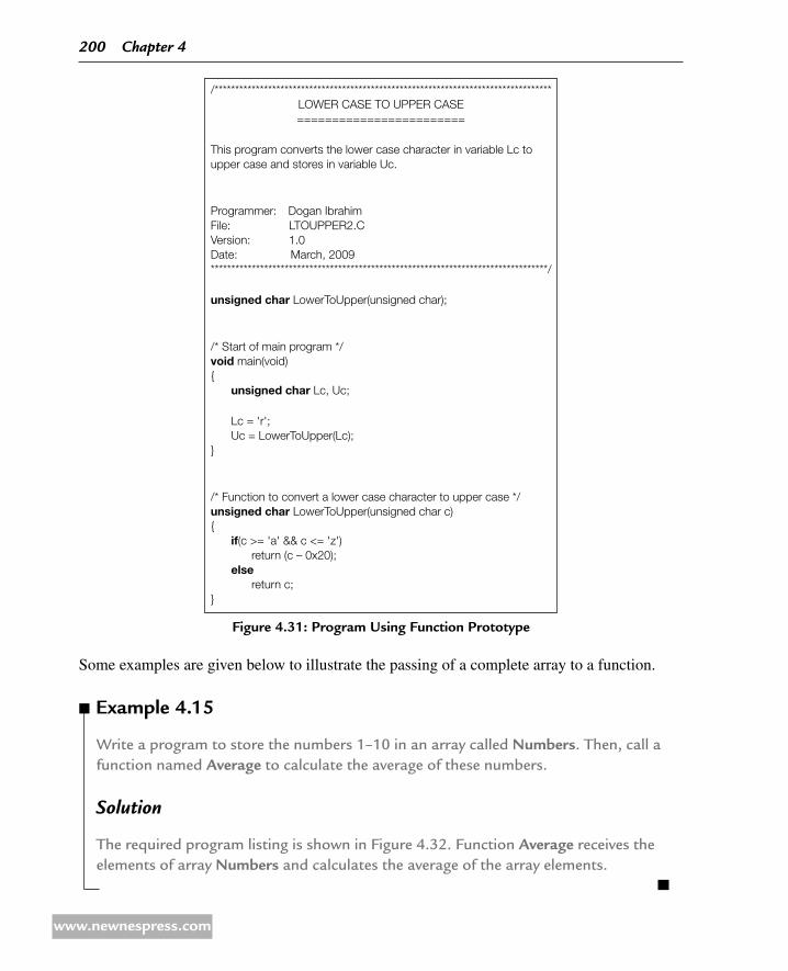
Some examples are given below to illustrate the passing of a complete array to a function.
example 4.15
Write a program to store the numbers 1–10 in an array called Numbers. Then, call a function named average to calculate the average of these numbers.
solution
The required program listing is shown in Figure 4.32. Function average receives the elements of array Numbers and calculates the average of the array elements.
Figure 4.31: Program Using Function Prototype
/**********************************************************************************LOWER CASE TO UPPER CASE========================
This program converts the lower case character in variable Lc to upper case and stores in variable Uc.
Programmer: Dogan IbrahimFile: LTOUPPER2.CVersion: 1.0Date: March, 2009**********************************************************************************/
unsigned char LowerToUpper(unsigned char);
/* Start of main program */void main(void)
unsigned char Lc, Uc;
Lc = 'r';Uc = LowerToUpper(Lc);
/* Function to convert a lower case character to upper case */unsigned char LowerToUpper(unsigned char c)
if(c >= 'a' && c <= 'z')return (c – 0x20);
elsereturn c;
200 Chapter 4
www.newnespress.com

example 4.16
Repeat Example 4.15, but this time define the array size at the beginning of the program and then pass the array size to the function.
solution
The required program listing is shown in Figure 4.33.
Figure 4.32: Program Passing an array to a Function
/********************************************************************************************PASSING AN ARRAY TO A FUNCTION============================
This program stores numbers 1 to 10 in an array called Numbers. Function Average is then called to calculate the average of these numbers.
Programmer: Dogan IbrahimFile: AVERAGE.CVersion: 1.0Date: March, 2009********************************************************************************************/
/* Function to calculate the average */float Average(int A[ ])
float Sum = 0.0, k;unsigned char j;
for ( j=0; j<10; j++)
Sum = Sum + A[ j ];k = Sum / 10.0;return k;
/* Start of the main program */void main(void)
unsigned char j;float Avrg;int Numbers[10];
for( j=0; j<10; j++)Numbers[ j ] = j+1;Avrg = Average(Numbers);
Programming with the MPLAB C18 Compiler 201
www.newnespress.com
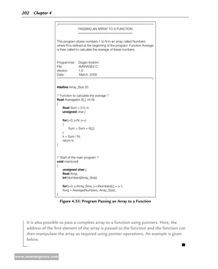
It is also possible to pass a complete array to a function using pointers. Here, the address of the first element of the array is passed to the function and the function can then manipulate the array as required using pointer operations. An example is given below.
Figure 4.33: Program Passing an array to a Function
/************************************************************************************PASSING AN ARRAY TO A FUNCTION============================
This program stores numbers 1 to N in an array called Numbers where N is defined at the beginning of the program. Function Average is then called to calculate the average of these numbers.
Programmer: Dogan IbrahimFile: AVERAGE2.CVersion: 1.0Date: March, 2009************************************************************************************/
#define Array_Size 20
/* Function to calculate the average */float Average(int A[ ], int N)
float Sum = 0.0, k;unsigned char j;
for( j=0; j<N; j++)
Sum = Sum + A[ j ];k = Sum / N;return k;
/* Start of the main program */void main(void)
unsigned char j;float Avrg;int Numbers[Array_Size];
for( j=0; j<Array_Size; j++)Numbers[ j ] = j+1;Avrg = Average(Numbers, Array_Size);
202 Chapter 4
www.newnespress.com

example 4.17
Repeat Example 4.15, but this time, use a pointer to pass the array elements to the function.
solution
The required program listing is given in Figure 4.34. Here, an integer pointer is used to pass the array elements to the function and the function elements are manipulated
Figure 4.34: Program Passing an array Using Pointers
/*******************************************************************************************PASSING AN ARRAY TO A FUNCTION============================
This program stores numbers 1 to 10 in an array called Numbers. FunctionAverage is then called to calculate the average of these numbers.
Programmer: Dogan IbrahimFile: AVERAGE3.CVersion: 1.0Date: March, 2009*******************************************************************************************/
/* Function to calculate the average */float Average(int *A)
float Sum = 0.0, k;unsigned char j;
for( j=0; j<10; j++)
Sum = Sum + *(A + j);k = Sum / 10.0;return k;
/* Start of the main program */void main(void)
unsigned char j;float Avrg;int Numbers[10];
for( j=0; j<10; j++)Numbers[ j ] = j+1;Avrg = Average(&Numbers[0]);
Programming with the MPLAB C18 Compiler 203
www.newnespress.com
using pointer operations. Notice that the address of the first element of the array is passed as an integer with the statement: &Numbers[0]
483 Passing Variables by Reference to Functions
By default, arguments to functions are passed by value. Although this method has many distinct advantages, there are occasions when it is more appropriate and also more efficient to pass the address of the arguments instead, that is, pass the argument by reference. When the address of an argument is passed, the original value of that argument can be modified by the function, and thus, the function does not have to return any variables. An example is given below, which illustrates how the address of arguments can be passed to a function and how the values of these arguments can be modified inside the function.
example 4.18
Write a function named Swap to accept two integer arguments and then to swap the values of these arguments. Use this function in a main program to swap the values of two variables.
solution
The required program listing is shown in Figure 4.35. Function Swap is defined as void since it does not return any value and it has two arguments a and b, and in the function header, two integer pointers are used to pass the addresses of these variables. Inside the function body, the value of an argument is accessed by inserting “*” character before the argument. Inside the main program, the address of the variables are passed to the function using the “&” characters before the variable names. At the end of the program, variables p and q are set to 20 and 10, respectively.
484 static Function Variables
Normally, variables declared at the beginning of a program, before the main program, are global, and their values can be accessed and modified by all parts of the program. Declaring a variable used in a global function will ensure that its value is retained from one call of the function to another, but this would undermine the variable’s privacy and reduce the portability of the function to other applications. A better approach is to declare such variables as static. Static variables are mainly used in function definitions. When a variable is declared as static,
204 Chapter 4
www.newnespress.com

its value is retained from one call of the function to another. In the example code given below, variable k is declared as static and is initialized to zero. This variable is then incremented before exiting from the function, and the value of k remains in existence and holds its last value on the next call to the function; i.e., on the second call to the function, the value of k will be 1 and not 0:
void Cnt(void)
static int k = 0; // Declare k as static……………….……………….k++; // increment k
Figure 4.35: Passing Variables by reference to a Function
/***********************************************************************************************PASSING VARIABLES BY REFERENCE=============================
This program shows how the address of variables can be passed to functions. The function in this program swaps the values of two integer variables.
Programmer: Dogan IbrahimFile: SWAP.CVersion: 1.0Date: March, 2009***********************************************************************************************/
/* Function to swap two integers */void Swap(int *a, int *b)
int temp;
temp = *a; // Store a in temp*a = *b; // Copy b to a*b = temp; // Copy temp to b
/* Start of the main program */void main(void)
int p, q;
p = 10; // Set p = 10q = 20; // Set q = 20swap(&p, &q); // Swap p and q (p=20, q=10)
Programming with the MPLAB C18 Compiler 205
www.newnespress.com
4.9 MPLaB C18 Library Functions
C18 compiler provides a large set of library functions that can be used in our programs. These library functions can be called from anywhere in a program, and they require the correct header files to be included at the beginning of the program. C18 manual MPLAB C18 C Compiler Libraries by Microchip Inc. gives detailed description of each library function.
C18 library functions are given as in the following headings:
Hardware Peripheral Functions Library •
Software Peripheral Functions Library •
General Software Library •
Math Library •
Hardware Peripheral Functions Library consists of functions for the following peripherals:
Analog-to-Digital (A/D) •
Input capture •
Integrated Interconnect ( I • 2C) bus
I/O port •
Microwire bus •
Pulse width modulation ( PWM • )
Serial peripheral interface (SPI) bus •
Timer •
Universal synchronous-asynchronous receiver-transmitter (USART) •
Software Peripheral Functions Library consists of functions for the following peripherals:
LCD •
CAN bus •
I • 2C bus
SPI bus •
UART •
206 Chapter 4
www.newnespress.com

General Software Library consists of functions for the following general-purpose operations:
Character classification •
Data conversion •
Memory and string manipulation •
delay •
Reset •
Character output •
Math Library consists of functions for the following:
A 32-bit floating point math library •
C Standard library math functions •
In this section, the description of some commonly used library functions are given with examples.
491 Delay Functions
These functions are used to create delays in programs. Table 4.8 gives a list of the available C18 delay functions. The header file “delays.h” must be included at the beginning of the pro-gram when any of these functions are used. The arguments of the functions must be an 8-bit unsigned character, i.e., the maximum allowed number in an argument is 255.
The delays are specified in terms of instruction cycle times. For example, when using a 4-MHz clock, the instruction cycle time is 1 μs. Thus, calling function
Delay100TCYx(5)
will cause 100 1 5 500 μs of delay in the program.
Similarly, to generate a 1-s delay when using a 4-MHz clock, we can call the function
Delay10KTCYx(100)
Functions descriptions
Delay1TCY Delay in one instruction cycle
Delay10TCYx Delay in multiples of 10 instruction cycles
Delay100TCYx Delay in multiples of 100 instruction cycles
Delay1KTCYx Delay in multiples of 1000 instruction cycles
Delay10KTCYx Delay in multiples of 10 000 instruction cycles
table 4.8: C18 delay Functions
Programming with the MPLAB C18 Compiler 207
www.newnespress.com

With an 8-MHz clock, the required function to generate a 1-s delay is
Delay10KTCYx(200)
Some examples given below show the use of delay functions in programs.
example 4.19
An LED is connected to bit 0 of PORTB (pin RB0) of a PIC18F452 microcontroller through a current limiting resistor as shown in Figure 4.36. Choose a suitable value for the resistor and write a program that will flash the LED ON and OFF continuously with 1-s intervals.
solution
LEDs can be connected to a microcontroller in two modes: current sinking mode and current sourcing mode. In current sinking mode (see Figure 4.37), one leg of the LED is connected to +5 V and the other leg is connected to the microcontroller output port pin through a current limiting resistor R.
Figure 4.36: Led Connected to Port rB0 of a PiC Microcontroller
15 V
VCC
RB0
LEDR
290
GND
PIC18F452
OSC1 OSC2
4 MHzresonator
208 Chapter 4
www.newnespress.com

Under normal working conditions, the voltage across an LED is approximately 2 V, and the current through the LED is approximately 10 mA (some low-power LEDs can oper-ate at as low as 1 mA current). The maximum current that can be sourced or sinked at the output port of a PIC microcontroller is 25 mA.
The value of the current limiting resistor R can be calculated as follows. In current sink-ing mode, the LED will be turned ON when the output port of the microcontroller is at logic 0, i.e., at approximately 0 V. The required resistor is then
R = 5 V − 2 V 10 mA = 0.3 K
The nearest resistor to choose is 290 (a slightly higher resistor can be chosen for a lower current and less brightness).
In current sourcing mode (see Figure 4.38), one leg of the LED is connected to the output port of the microcontroller and the other leg is connected to ground through a current limiting resistor. The LED will be turned ON when the output port of the
Figure 4.37: Connecting the Led in Current Sinking Mode
15 V
LED
R
PIC
Figure 4.38: Connecting the Led in Current Sourcing Mode
LED
R
PIC
Programming with the MPLAB C18 Compiler 209
www.newnespress.com

microcontroller is at logic 1, i.e., at approximately 5 V. Both in current sinking and in current sourcing modes, we can use the same value resistor.
The required program listing is given in Figure 4.39 (program FLASH.C). At the beginning of the program, device-specific header file “p18f452.h” and delay header file “delays.h” are included. Then, PORTB is configured as output using the TRISB = 0 statement. An endless loop is then formed with the for statement, and inside this loop, the LED is turned ON and OFF with 1-s delay between each output. The microcontroller is operated with a 4-MHz clock and thus the instruction cycle time is 1 μs. Function Delay10KTCYx is called as described earlier with an argument of 100 to generate a 1-s delay.
The program given in Figure 4.39 can be made more user friendly and easier to follow using defined statements as shown in Figure 4.40 (program FLASH2.C).
/****************************************************************************************************FLASHING AN LED==============
This program flashes an LED connected to port RB0 of a microcontroller with one second intervals. C18 library function Delay10KTCYx is used to create a 1 second delay between the flashes.
A 4MHz clock is used in the project.
Programmer: Dogan IbrahimFile: FLASH.CVersion: 1.0Date: March, 2009****************************************************************************************************/#include <p18f452.h>#include <delays.h>
void main(void)
TRISB = 0; // Configure PORTB as outputfor(; ;) // Endless loop
PORTB = 1; // Turn ON LEDDelay10KTCYx(100); // 1 second delayPORTB = 0; // Turn OFF LEDDelay10KTCYx(100); // 1 second delay
Figure 4.39: Program to Flash an Led
210 Chapter 4
www.newnespress.com

Functions descriptions
isalnum Determines if a character is alphanumeric
isalpha Determines if a character is alphabetic
isdigit Determines if a character is a decimal digit
islower Determines if a character is lowercase
isupper Determines if a character is uppercase
table 4.9: Some Character Classification Functions
/****************************************************************************************FLASHING AN LED==============
This program flashes an LED connected to port RB0 of a microcontroller with one second intervals. C18 library function Delay10KTCYx is used to create a 1 second delay between the flashes.
Programmer: Dogan IbrahimFile: FLASH2.CVersion: 1.0Date: March, 2009****************************************************************************************/#include <p18f452.h>#include <delays.h>
#define LED PORTBbits.RB0#define ON 1#define OFF 0#define One_Second_Delay Delay10KTCYx(100)
void main(void)
TRISB = 0; // Configure PORT B as output
for(; ;) // Endless loop
LED = ON; // Turn ON LEDOne_Second_Delay; // 1 second delayLED = OFF; // Turn OFF LEDOne_Second_Delay; // 1 second delay
Figure 4.40: another Program to Flash an Led
492 Character Classification Functions
These functions can be used to test the nature of characters. Table 4.9 shows some of the functions in this library. The header file “ctype.h” must be included at the beginning of the program whenever one of these functions is used.
Programming with the MPLAB C18 Compiler 211
www.newnespress.com
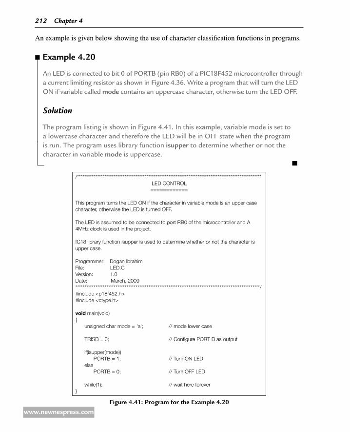
An example is given below showing the use of character classification functions in programs.
example 4.20
An LED is connected to bit 0 of PORTB (pin RB0) of a PIC18F452 microcontroller through a current limiting resistor as shown in Figure 4.36. Write a program that will turn the LED ON if variable called mode contains an uppercase character, otherwise turn the LED OFF.
solution
The program listing is shown in Figure 4.41. In this example, variable mode is set to a lowercase character and therefore the LED will be in OFF state when the program is run. The program uses library function isupper to determine whether or not the character in variable mode is uppercase.
Figure 4.41: Program for the example 4.20
/*****************************************************************************************************LED CONTROL============
This program turns the LED ON if the character in variable mode is an upper case character, otherwise the LED is turned OFF.
The LED is assumed to be connected to port RB0 of the microcontroller and A 4MHz clock is used in the project.
fC18 library function isupper is used to determine whether or not the character is upper case.
Programmer: Dogan IbrahimFile: LED.CVersion: 1.0Date: March, 2009*****************************************************************************************************/#include <p18f452.h>#include <ctype.h>
void main(void)
unsigned char mode = 'a'; // mode lower case
TRISB = 0; // Configure PORT B as output
if(isupper(mode))PORTB = 1; // Turn ON LED
elsePORTB = 0; // Turn OFF LED
while(1); // wait here forever
212 Chapter 4
www.newnespress.com

493 Data Conversion Functions
These functions can be used to convert one type of data into another type. Table 4.10 shows some of the functions in this library. The header file “stdlib.h” or “ctype.h” must be included at the beginning of the program whenever one of these functions is used.
An example is given below showing the use of data conversion functions in programs.
example 4.21
A character array named my_str contains five lowercase ASCII characters. Write a program that will convert all the characters in this array into uppercase.
solution
The program listing is shown in Figure 4.42. In this example, data conversion function toupper is used to convert the characters to uppercase. Notice that the header file “ctype.h” is included at the beginning of the program.
494 Memory and string Manipulation Functions
These functions can be used to search for a given value in the memory, to compare two arrays, to compare two strings, initialize an array, determine the length of a string, and so on. Table 4.11 shows some of the functions in this library. The header file “string.h” must be included at the beginning of the program whenever one of these functions is used.
An example is given below showing the use of memory and string manipulation functions in programs.
Functions descriptions
atoi Converts a string into a 16-bit signed integer
atol Converts a string into a long integer
itoa Converts a 16-bit signed integer into a string
tolower Converts a character to lowercase
toupper Converts a character to uppercase
table 4.10: Some data Conversion Functions
Programming with the MPLAB C18 Compiler 213
www.newnespress.com

example 4.22
A string named my_str contains various lowercase and uppercase ASCII characters. Write a program that will convert all the characters in this array into uppercase.
solution
The program listing is shown in Figure 4.43. In this example, string manipulation func-tion strupr is used to convert the characters to uppercase. Notice that the header file “string.h” is included at the beginning of the program.
Figure 4.42: Program for example 4.21
/***************************************************************************************UPPER CASE==========
This program converts the 5 characters in array my_str into upper case.
C18 library function toupper is used in the program.
Programmer: Dogan IbrahimFile: UPPER.CVersion: 1.0Date: March, 2009***************************************************************************************/#include <p18f452.h>#include <ctype.h>
void main(void)
unsigned char my_str[5] = 'a','s','e','r','w';unsigned char k;
for(k = 0; k < 5; k++)my_str[k] = toupper(my_str[k]);
while(1); // wait here forever
Functions descriptions
memcmp Compares the contents of two arrays
memset Initializes an array with a repeated value
strchr Locates the first occurrence of a value in a string
strlen Determines the length of a string
strstr Locates the first occurrence of a string inside another string
strupr Coverts all characters in a string to uppercase
table 4.11: Some data Conversion Functions
214 Chapter 4
www.newnespress.com

example 4.23
Write a program to find the length of a string called my_str and store it in a character variable called slen.
solution
The program listing is shown in Figure 4.44. In this example, function strlen is used to find the length of the string. The string is “MyString” and thus slen is assigned number 8.
example 4.24
Assume that a string called First contains data “PIC” and another string called Second contains data “Microcontroller.” Write a program to append string Second to string First. Thus, at the end of the operation, string First will have data “PIC Microcontroller” and string Second will not change, i.e., it will have the data “Microcontroller.”
/**********************************************************************************************UPPER CASE===========
This program converts the characters in string my_str into upper case.
C18 library function strupr is used in the program.
Programmer: Dogan IbrahimFile: UPPER.CVersion: 1.0Date: March, 2009**********************************************************************************************/#include <p18f452.h>#include <string.h>
void main(void)
char my_str[ ] = "MyString"; // Declare string my_str
strupr(my_str); // my_str = "MYSTRING"
while(1); // Wait here forever
Figure 4.43: Program for the example 4.22
Programming with the MPLAB C18 Compiler 215
www.newnespress.com

solution
The program listing is shown in Figure 4.45. In this example, function strcat is used to append one string to another string. You should make sure that the destination string (First) is large enough to hold the source string (Second).
495 Reset Functions
These functions are used to determine the cause of reset or wake up in a program. Table 4.12 shows some of the functions in this library. The header file “reset.h” must be included at the beginning of the program whenever one of these functions is used.
An example is given below showing the use of reset functions in programs.
Figure 4.44: Program for the example 4.23
/*******************************************************************************************STRING LENGTH=============
This program finds the length of string my_str and stores in variable slen. String my_str is loaded with "MyString", having 8 characters and thus Variable slen will be set to 8.
C18 library function strlen is used in the program.
Programmer: Dogan IbrahimFile: LEN.CVersion: 1.0Date: March, 2009*******************************************************************************************/#include <p18f452.h>#include <string.h>
void main(void)
char my_str[ ] = "MyString"; // Declare string my_strunsigned char slen;
slen = strlen(my_str); // Length of the string
while(1); // Wait here forever
216 Chapter 4
www.newnespress.com

example 4.25
Write a program to determine the cause of reset in a program. If the cause of reset is Master Clear (MCLR) input or power-on reset, then load variable rst with 1, otherwise load rst with 0.
solution
The program listing is shown in Figure 4.46.
Figure 4.45: Program for the example 4.24
/**************************************************************************************************STRING APPEND=============
String First is loaded with "PIC" and string Second is loaded with "Microcontroller". The program appends string Second to string First so that First contains the characters "PIC Microcontroller". String Second does not change.
C18 library function strcat is used in the program.
Programmer: Dogan IbrahimFile: StrLen.CVersion: 1.0Date: March, 2009***************************************************************************************************/#include <p18f452.h>#include <string.h>
void main(void)
char First[20] = "PIC "; // String Firstchar Second[ ] = "Microcontroller"; // String Second
strcat(First, Second); // Append strings
while(1); // Wait here forever
table 4.12: Some reset Functions
Functions descriptions
isMCLR If the cause of reset was MCLR
isPOR If the cause of reset was power-on reset
isWDTTO If the cause of reset was the watchdog timeout
Programming with the MPLAB C18 Compiler 217
www.newnespress.com

496 Character Output Functions
These functions are used to process the output to various peripheral devices. Table 4.13 shows some of the functions in this library. The header file “stdio.h” must be included at the begin-ning of the program whenever one of these functions is used. Note that the data is sent to the
table 4.13: Some Character Output Functions
Functions descriptions
printf Formatted output to stdout
putc Character output to a string
puts String output to stdout
sprintf Formatted string output to a data memory buffer
_usart_putc Single character output to USART
Figure 4.46: Program for the example 4.25
/**********************************************************************************************RESET=====
This program determines the cause of reset in a program.
If the cause of Reset is MCLR or Power-on-reset then load variable Rst with 1, otherwise load Rst with 0.
C18 library functions is MCLR and isPOR are used in the program.
Programmer: Dogan IbrahimFile: Reset.CVersion: 1.0Date: March, 2009**********************************************************************************************/#include <p18f452.h>#include <reset.h>
void main(void)
unsigned char Rst;
if(isMCLR || isPOR) // Cause MCLR or Power-on-reset ?Rst = 1; // Load Rst with 1
elseRst = 0; // Load Rst with 0
while(1); // Wait here forever
218 Chapter 4
www.newnespress.com

device defined by the standard output stdout. The stdout is defined, by default, as the device _H_USART, which is the USART.
Some examples are given below to show the use of character output functions.
example 4.26
Write a program to send the message “My Microcontroller” to the USART device of a PIC18F452 microcontroller.
solution
The program listing is shown in Figure 4.47. Function printf is used to send the string to USART. This function can have a large number of arguments to format the data. Some of the commonly used formatting arguments are as follows:
%c character
%d integer number
%o octal number
%u unsigned integer number
%b binary number
%x hexadecimal number
%s string
%f floating point number
example 4.27
Write a program to count up in decimal from 0 to 10 and send the output to the USART in the following format:
Number = nn,
where nn is the number 0–10
solution
The program listing is shown in Figure 4.48. Function printf is used to send the string to USART with the argument “%d.” Note that a new-line character “\n” is used at the end of each output.
Programming with the MPLAB C18 Compiler 219
www.newnespress.com

/**************************************************************************Character Output=============
This program counts up from 00 to 10 and sends the result to USART in the Following format:
Number = nnC18 library function printf is used in the program.
Programmer: Dogan IbrahimFile: Count.CVersion: 1.0Date: March, 2009**************************************************************************/#include <p18f452.h>#include <stdio.h>
void main(void)
unsigned char cnt;
for(cnt=0; cnt <= 10; cnt++) printf("Number = %d\n", cnt);
while(1); // Wait here forever
Figure 4.48: Program for the example 4.27
/**************************************************************************************Character Output============
This program sends the message "My Microcontroller" to the standard output device of the microcontroller, which is the USART.
C18 library function printf is used in the program.
Programmer: Dogan IbrahimFile: Cout.CVersion: 1.0Date: March, 2009**************************************************************************************/#include <p18f452.h>#include <stdio.h>
void main(void)
printf("My Microcontroller");
while(1); // Wait here forever
Figure 4.47: Program for example 4.26
220 Chapter 4
www.newnespress.com

If the debugger UART window is enabled (Debugger -> Settings -> Uart IO -> Enable Uart IO -> Window), then the following text will be displayed in the I/O panel:
Number = 0
Number = 1
Number = 2
Number = 3
Number = 4
Number = 5
Number = 6
Number = 7
Number = 8
Number = 9
Number = 10
example 4.28
Write a program to count up in decimal from 0 to 20 and send the output to USART in the following hexadecimal format:
Number = nn,
where nn is the number 0–0x14
solution
The program listing is shown in Figure 4.49. Function printf is used to send the string to USART with the argument “%d.” Note that a new-line character “\n” is used at the end of each output.
If the debugger UART window is enabled then the following text will be displayed in the I/O panel:
Number = 0
Number = 1
Number = 2
Number = 3
Number = 4
Number = 5
Number = 6
Number = 7
Programming with the MPLAB C18 Compiler 221
www.newnespress.com

Number = 8
Number = 9
Number = a
Number = b
Number = c
Number = d
Number = e
Number = f
497 Math Library Functions
These are trigonometric, logarithmic, and power functions. Table 4.14 shows some of the functions in this library. The header file “math.h” must be included at the beginning of every program using these functions.
Figure 4.49: Program for example 4.28
/***************************************************************************Character Output=============
This program counts up from 0 to 120 and sends the result to USART in the following hexadecimal format:
Number = nn
Where nn is 0 to 0x14.
C18 library function printf is used in the program.
Programmer: Dogan IbrahimFile: HexCount.CVersion: 1.0Date: March, 2009***************************************************************************/#include <p18f452.h>#include <stdio.h>
void main(void)
unsigned char cnt;
for(cnt=0; cnt <= 20; cnt++) printf("Number = %x\n", cnt);
while(1); // Wait here forever
222 Chapter 4
www.newnespress.com

Some examples are given below to show how these functions can be used in programs.
example 4.29
Write a program to calculate the trigonometric sine of 30° and store the result in a variable called angle.
solution
The program listing is shown in Figure 4.50. It is important to note that the angles must be represented in radians and not in degrees. To convert degrees into radians, we can multiply the angle with π (3.14159) and divide by 180. The answer 0.5 is stored in variable angle.
example 4.30
Write a program to calculate the squares of numbers from 0 to 10 and send the result to USART as a table in the following format:
0 0
1 1
2 4
3 9
4 1
………………...
………………...
………………...
10 100
table 4.14: Some Math Library Functions
Functions descriptions
sin Trigonometric sine
cos Trigonometric cosine
tan Trigonometric tangent
asin Trigonometric inverse of sine
acos Trigonometric inverse of cosine
cosh Hyperbolic cosh
log Natural logarithm
exp Exponential factor
Programming with the MPLAB C18 Compiler 223
www.newnespress.com

solution
The program listing is shown in Figure 4.51. Function pow is used in a for loop with arguments (k, 2.0) so that the squares of numbers k are calculated. The numbers are sent to USART in a table format using the printf function. Notice that both “stdio.h” and “math.h” header files are included at the beginning of the program.
The USART data can be displayed by enabling the USART in the debugger. The data will be displayed as shown below:
0 0
1 1
2 4
3 9
4 16
5 25
6 36
Figure 4.50: Program for the example 4.29
/*************************************************************************************** Trigonometric Sine==============
This program calculates the trigonometric sine of 30 degrees and stores the Result in variable called angle.
C18 library function sin is used in the program.
Programmer: Dogan IbrahimFile: Sine.CVersion: 1.0Date: March, 2009***************************************************************************************/#include <p18f452.h>#include <math.h>
void main(void)
float angle;float Pi = 3.14159; // Pifloat Conv = 3.14159 / 180.0; // Conversion factor
angle = sin(30.0 * Conv); // angle 0.5
while(1); // Wait here forever
224 Chapter 4
www.newnespress.com

7 49
8 64
9 81
10 100
498 LCD Functions
All microcontrollers lack some kind of video display. A video display would make a microcon-troller much more user friendly as it will enable text messages, graphics, and numeric values to be output in a more versatile manner than the seven-segment displays, LEDs, or alphanumeric dis-plays. Standard video displays require complex interfaces and their cost is relatively high. LCDs are alphanumeric (or graphical) displays, which are frequently used in microcontroller-based
/**************************************************************************************Squares of Numbers
================
This program calculates the squares of integer numbers from 0 to 10 and sends the results to USART in a table form.
C18 library function pow and printf are used in the program.
Programmer: Dogan IbrahimFile: Powers.CVersion: 1.0Date: March, 2009**************************************************************************************/#include <p18f452.h>#include <math.h>#include <stdio.h>
void main(void)
unsigned char k;unsigned int Number;
for(k = 0; k<= 10; k++)
Number = pow(k , 2.0);printf("%d %d\n", k, Number);
while(1); // Wait here forever
Figure 4.51: Program for the example 4.30
Programming with the MPLAB C18 Compiler 225
www.newnespress.com
applications. These display devices come in different shapes and sizes. Some LCDs have 40 or more character lengths with the capability to display several lines. Some other LCD displays can be programmed to display graphic images. Some modules offer color displays, while some others incorporate back lighting so that they can be viewed in dimly lit conditions.
There are basically two types of LCDs as far as the interfacing technique is concerned: parallel LCDs and serial LCDs. Parallel LCDs (e.g., Hitachi HD44780 series) are connected to the microcontroller circuitry such that data is transferred to the LCD using more than one line, and usually, four or eight data lines are used. Serial LCD is connected to a microcon-troller using one data line only and data is transferred using the RS232 asynchronous data communications protocol. Serial LCDs are generally much easier to use, but they are more costly than the parallel ones. In this book, only the parallel LCDs will be considered, as they are cheaper and are used more commonly in microcontroller-based projects.
Low-level programming of a parallel LCD is usually a complex task and requires a good understanding of the internal operation of the LCD, including an understanding of the timing diagrams. Fortunately, C18 language provides library functions for text-based LCDs, which simplify the use of external LCDs in PIC microcontroller-based projects.
HD44780 controller is commonly used in parallel LCD-based microcontroller applications. A brief description of this controller and information on some commercially available LCD modules is given below.
HD44780 LCD Controller
HD44780 is one of the most popular LCD controllers used in many LCD modules in indus-trial and commercial applications and also by hobbyists. The module is monochrome and comes in different shapes and sizes. Modules with character lengths of 8, 16, 20, 24, 32, and 40 can be selected. Depending on the model chosen, the display provides a 14-pin or a 16-pin connector to interface to the external world. Table 4.15 shows the pin configuration and pin functions of a typical 14-pin LCD.
VSS is the 0 V supply or ground. Vdd pin should be connected to the positive supply. Although the manufacturers specify a 5-V DC supply, the modules will usually work with as low as 3 V or as high as 6 V.
Pin 3 is named as Vee, and this is the contrast control pin. This pin is used to adjust the con-trast of the display and it should be connected to a DC supply. A potentiometer is usually connected to the power supply with its wiper arm connected to this pin and the other leg of the potentiometer connected to the ground. This way, the voltage at the Vee pin and hence the contrast of the display can be adjusted as desired.
Pin 4 is the Register Select (RS), and when this pin is LOW, data transferred to the LCD is treated as commands. When RS is HIGH, character data can be transferred to and from the module.
226 Chapter 4
www.newnespress.com

Pin 5 is the Read/Write (R/W) pin. This pin is pulled LOW to write commands or character data to the LCD module. When this pin is HIGH, character data or status information can be read from the module.
Pin 6 is the Enable (EN) pin that is used to initiate the transfer of commands or data between the module and the microcontroller. When writing to the display, data is transferred only on the HIGH to LOW transition of this pin. When reading from the display, data becomes avail-able after the LOW to HIGH transition of the enable pin, and this data remains valid as long as the enable pin is at logic HIGH.
Pins 7–14 are the eight data bus lines (D0–D7). Data can be transferred between the micro-controller and the LCD module either using a single, 8-bit byte or as two, 4-bit nibbles. In the latter case, only the upper four data lines (D4–D7) are used. The 4-bit mode has the advan-tage that fewer I/O lines are required to communicate with the LCD.
C18 LCD library provides large number of functions to control text-based LCDs with 4-bit and 8-bit data interface. Four-bit interface-based text LCDs are the most commonly used LCDs, and this section describes the important C18 functions to control and send data to these LCDs. Further information on other LCD functions can be obtained from the manual MPLAB C18 C Compiler Libraries.
Table 4.16 gives a list of the commonly used LCD functions available for 4-bit interface text-based LCDs. Note that the header file “xlcd.h” must be included at the beginning of a program when any of these functions are used.
table 4.15: Pin Configuration of the hd44780 LCd Module
Pin Nos Names Functions
1 VSS Ground
2 VDD +ve supply
3 VEE Contrast
4 RS Register select
5 R/W Read/write
6 EN Enable
7 D0 Data bit 0
8 D1 Data bit 1
9 D2 Data bit 2
10 D3 Data bit 3
11 D4 Data bit 4
12 D5 Data bit 5
13 D6 Data bit 6
14 D7 Data bit 7
Programming with the MPLAB C18 Compiler 227
www.newnespress.com

The LCD library requires that the following delay functions be defined by the user before using the LCD functions:
DelayFor18TCY Delay for 18 cycles
DelayPORXLCD Delay for 15 ms
DelayXLCD Delay for 5 ms
Assuming a microcontroller clock frequency of 4 MHz, the instruction cycle time is 1 µs. With a clock frequency of 8 MHz, the instruction cycle time is 0.5 μs. Figure 4.52 shows how the above delay functions could approximately be obtained for both 4 and 8-MHz clock frequencies. The 18-cycle delay is obtained using no operation (NOP) statements, where each NOP operation takes one cycle to execute. The end of a function with no “return” statement takes two cycles. When a “return” statement is used, a BRA statement branches to the end of the function where a RETURN 0 is executed to return from the function, thus adding two more cycles. For example, the following function takes four cycles to execute:
void test(void) nop( ); ;1 cycle nop( ); ;1 cycle ; RETURN 0, takes 2 cycles
and the following function takes six cycles to execute:
void test(void) nop( ); ; 1 cycle nop( ); ; 1 cycle return; ; BRA X, 2 cycles ; X: RETURN 0, 2 cycles
A brief description of the C18 LCD functions is given below.
BusyXLCD
This function checks to determine whether or not the LCD controller is busy, and data or commands should not be sent to the LCD if the controller is busy. The function returns 1 if
table 4.16: Commonly Used LCd Functions
Functions descriptions
BusyXLCD Checks if the LCD controller is busy
OpenXLCD Configures I/O port lines for the LCD and initializes
putcXLCD Writes a byte of data to the LCD
putsXLCD Writes a string from data memory to the LCD
putrsXLCD Writes a string from program memory to the LCD
WriteCmdXLCD Writes a command to the LCD
228 Chapter 4
www.newnespress.com

Figure 4.52: LCd delay Functions for 4-Mhz and 8-Mhz Clock
4MHz Clock
#include<delays.h>
void DelayFor18TCY(void) Nop( ); Nop( ); Nop( ); Nop( ); // 18 cycle delay Nop( ); Nop( ); Nop( ); Nop( ); Nop( ); Nop( ); Nop( ); Nop( ); Nop( ); Nop( ); return;
void DelayPORXLCD(void) // 15ms delay Delay1KTCYx(15);
void DelayXLCD(void) Delay1KTCYx(5); // 5ms delay
8MHz Clock
#include <delays.h>
void Delayfor18TCY(void) Nop( ); Nop( ); Nop( ); Nop( ); // 18 cycle delay Nop( ); Nop( ); Nop( ); Nop( ); Nop( ); Nop( ); Nop( ); Nop( ); Nop( ); Nop( ); return;
void DelayPORXLCD(void) // 15ms delay Delay1KTCYx(30);
void DelayXLCD(void) Delay1KTCYx(10); // 5ms delay
Programming with the MPLAB C18 Compiler 229
www.newnespress.com
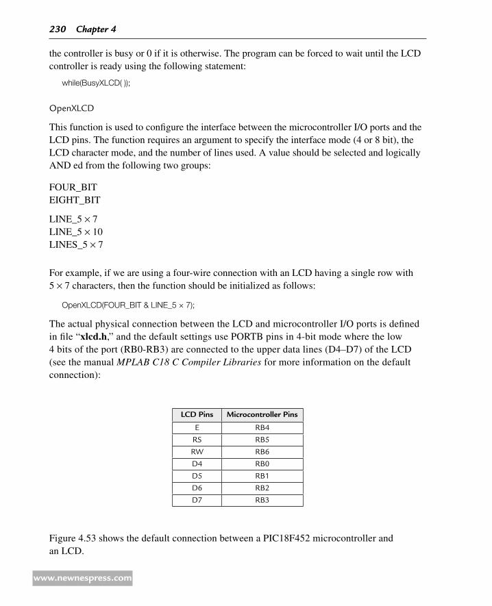
the controller is busy or 0 if it is otherwise. The program can be forced to wait until the LCD controller is ready using the following statement:
while(BusyXLCD( ));
OpenXLCD
This function is used to configure the interface between the microcontroller I/O ports and the LCD pins. The function requires an argument to specify the interface mode (4 or 8 bit), the LCD character mode, and the number of lines used. A value should be selected and logically AND ed from the following two groups:
FOUR_BITEIGHT_BIT
LINE_5 × 7LINE_5 × 10LINES_5 × 7
For example, if we are using a four-wire connection with an LCD having a single row with 5 × 7 characters, then the function should be initialized as follows:
OpenXLCD(FOUR_BIT & LINE_5 × 7);
The actual physical connection between the LCD and microcontroller I/O ports is defined in file “xlcd.h,” and the default settings use PORTB pins in 4-bit mode where the low 4 bits of the port (RB0-RB3) are connected to the upper data lines (D4–D7) of the LCD (see the manual MPLAB C18 C Compiler Libraries for more information on the default connection):
LCd Pins Microcontroller Pins
E RB4
RS RB5
RW RB6
D4 RB0
D5 RB1
D6 RB2
D7 RB3
Figure 4.53 shows the default connection between a PIC18F452 microcontroller and an LCD.
230 Chapter 4
www.newnespress.com
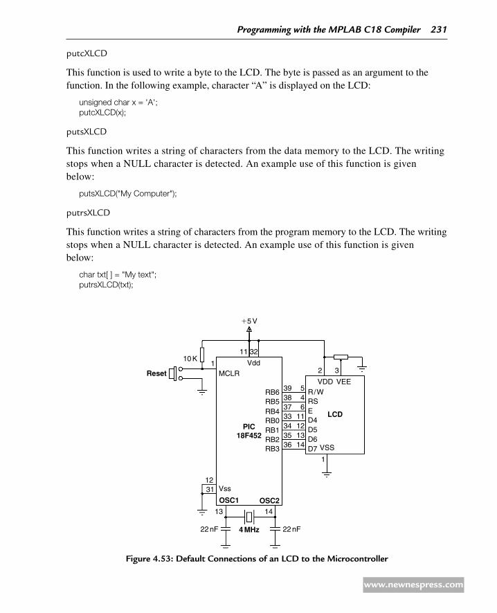
putcXLCD
This function is used to write a byte to the LCD. The byte is passed as an argument to the function. In the following example, character “A” is displayed on the LCD:
unsigned char x = 'A';putcXLCD(x);
putsXLCD
This function writes a string of characters from the data memory to the LCD. The writing stops when a NULL character is detected. An example use of this function is given below:
putsXLCD("My Computer");
putrsXLCD
This function writes a string of characters from the program memory to the LCD. The writing stops when a NULL character is detected. An example use of this function is given below:
char txt[ ] = "My text";putrsXLCD(txt);
Figure 4.53: default Connections of an LCd to the Microcontroller
15 V
Vdd
VDD
Vss
VSS
OSC2OSC1
R/WRSED4D5D6D7
LCD
VEE
PIC18F452
RB6 39383733343536
5
2 3
46
11121314
1
12
13
22 nF 22 nF4 MHz
14
31
RB5RB4RB0RB1RB2RB3
MCLRReset
10 K1
11 32
Programming with the MPLAB C18 Compiler 231
www.newnespress.com
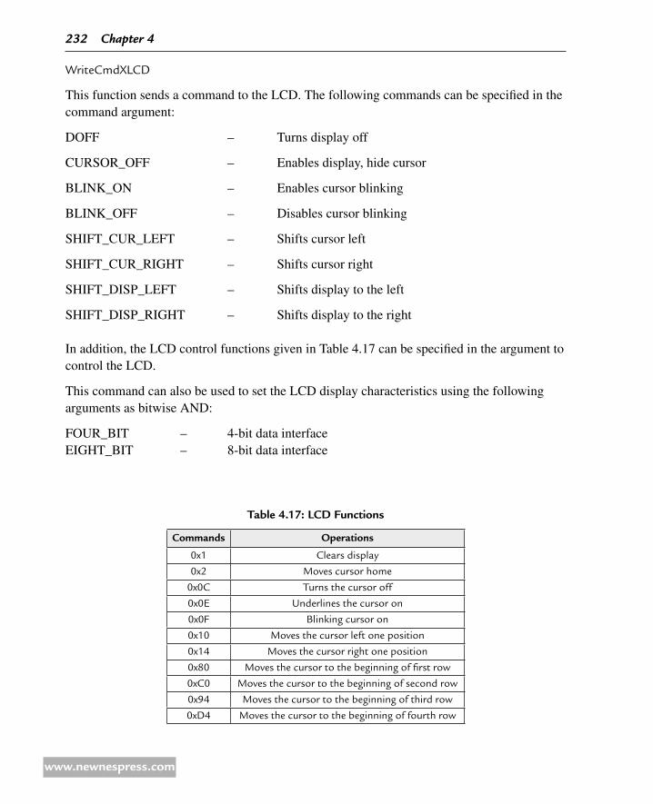
WriteCmdXLCD
This function sends a command to the LCD. The following commands can be specified in the command argument:
DOFF – Turns display off
CURSOR_OFF – Enables display, hide cursor
BLINK_ON – Enables cursor blinking
BLINK_OFF – Disables cursor blinking
SHIFT_CUR_LEFT – Shifts cursor left
SHIFT_CUR_RIGHT – Shifts cursor right
SHIFT_DISP_LEFT – Shifts display to the left
SHIFT_DISP_RIGHT – Shifts display to the right
In addition, the LCD control functions given in Table 4.17 can be specified in the argument to control the LCD.
This command can also be used to set the LCD display characteristics using the following arguments as bitwise AND:
FOUR_BIT – 4-bit data interfaceEIGHT_BIT – 8-bit data interface
table 4.17: LCd Functions
Commands Operations
0x1 Clears display
0x2 Moves cursor home
0x0C Turns the cursor off
0x0E Underlines the cursor on
0x0F Blinking cursor on
0x10 Moves the cursor left one position
0x14 Moves the cursor right one position
0x80 Moves the cursor to the beginning of first row
0xC0 Moves the cursor to the beginning of second row
0x94 Moves the cursor to the beginning of third row
0xD4 Moves the cursor to the beginning of fourth row
232 Chapter 4
www.newnespress.com

LINE_5 × 7 – 5 × 7 character modeLINE_5 × 10 – 5 × 10 character modeLINES_5 × 7 – 5 × 7 multiple line display
It is important that the LCD controller should not be busy (check with function BusyXLCD) when commands are sent to it. Some example commands are given below:
WriteCmdXL CD(EIGHT_BIT & LINE_5X7); // 8 bit, 5 × 7 characterWriteCmdXLCD(BLINK_ON); // Blink ONWriteCmdXLCD(1); // Clear LCD
A complete example is given below, which illustrates how the LCD can be initialized and used.
example 4.31
A text-based LCD is connected to a PIC18F452 microcontroller in the default mode as shown in Figure 4.53. Write a program to clear the LCD and then send the text “My Computer” to the LCD.
solution
The required program listing is given in Figure 4.54. The message to be displayed is stored in the character array msg. At the beginning of the program, PORTB is con-figured as output with the TRISB = 0 statement. The LCD is then initialized, display cleared, and the text message “My Computer” is displayed on the LCD. Notice that the LCD is cleared by sending command 1 to the LCD controller.
Modifying the Default Configuration
It may sometimes be required to use different ports for the LCD. In this section, an example is given to show how the default port configuration can be modified.
example 4.32
A text-based LCD is connected to a PIC18F452 microcontroller as shown in Figure 4.55. Show how the default configuration can be modified and write a program to count on the LCD from 0 to 99 with a delay of 1 s between each count. The display should be as follows:
NO = nn,
where nn is from 0 to 99.
Programming with the MPLAB C18 Compiler 233
www.newnespress.com
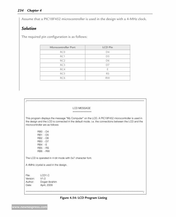
Assume that a PIC18F452 microcontroller is used in the design with a 4-MHz clock.
solution
The required pin configuration is as follows:
Microcontroller Port LCd Pin
RC0 D4
RC1 D5
RC2 D6
RC3 D7
RC4 E
RC5 RS
RC6 RW
/********************************************************************************************************************************
LCD MESSAGE ============
This program displays the message "My Computer" on the LCD. A PIC18F452 microcontroller is used in the design and the LCD is connected in the default mode. i.e. the connections between the LCD and the microcontroller are as follows:
RB0 - D4 RB1 - D5 RB2 - D6 RB3 - D7 RB4 - E RB5 - RS RB6 - RW
The LCD is operated in 4-bit mode with 5x7 character font.
A 4MHz crystal is used in the design.
File: LCD1.CVersion: V1.0Author: Dogan IbrahimDate: April, 2009
********************************************************************************************************************************/
Figure 4.54: LCd Program Listing
234 Chapter 4
www.newnespress.com

#include <p18f452.h>#include <xlcd.h>#include <delays.h>
#pragma config WDT = OFF#pragma config OSC = XT
//// Defines//#define CLR_LCD 1#define HOME_LCD 2
//// LCD Delays//void DelayFor18TCY(void)
Nop( ); Nop( ); Nop( ); Nop( ); // 18 cycle delayNop( ); Nop( ); Nop( ); Nop( );Nop( ); Nop( ); Nop( ); Nop( );Nop( ); Nop( );return;
void DelayPORXLCD(void) // 15ms delay
Delay1KTCYx(15);
void DelayXLCD(void)
Delay1KTCYx(5); // 5ms delay
/*================ Start of MAIN program ================ */
void main(void)
char msg[ ] = "My Computer";
OpenXLCD(FOUR_BIT & LINE_5X7); // 8 bit,5x7 characterWriteCmdXLCD(CLR_LCD); // Clear LCDwhile(BusyXLCD( ));WriteCmdXLCD(HOME_LCD); // Home cursorwhile(BusyXLCD( ));putsXLCD( msg ); // Write data
while(1);
Figure 4.54: Cont’d
Programming with the MPLAB C18 Compiler 235
www.newnespress.com

The first step is to modify the LCD configuration file xlcd.h. The steps are given below:
Copy file • xlcd.h to xlcd_default.h in directory C:\MCC18\h. The default LCD library is named as xlcd_default and is available if required.
Modify the following lines in file • xlcd.h to reflect the required interface between the microcontroller and the LCD:
#define DATA_PORT PORTC
#define TRIS_DATA_PORT TRISC
#define RW_PIN LATCbits.LATC6 /* PORT for RW */
#define TRIS_RW TRISCbits.TRISC6 /* TRIS for RW */
#define RS_PIN LATCbits.LATC5 /* PORT for RS */
#define TRIS_RS TRISCbits.TRISC5 /* TRIS for RS */
#define E_PIN LATCbits.LATC4 /* PORT for D */
#define TRIS_E TRISCbits.TRISC4 /* TRIS for E */
Start a command session. • Start -> run -> Cmd
Go to directory • C:\MCC18\src\
Figure 4.55: Circuit diagram for the example 4.32
15 V
Vdd
VDD
Vss
VSS
OSC2OSC1
R/WRSED4D5D6D7
LCD
VEE
PIC18F452
RC6 25242315161718
5
2 3
46
11121314
1
12
13
22 nF 22 nF4 MHz
14
31
RC5RC4RC0RC1RC2RC3
MCLRReset
10 K1
11 32
236 Chapter 4
www.newnespress.com
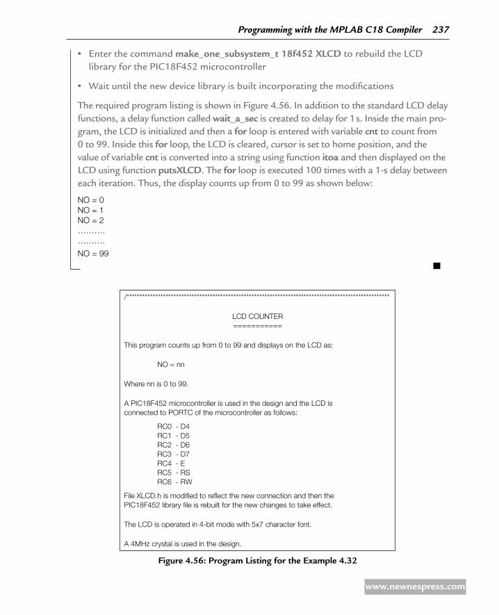
Enter the command • make_one_subsystem_t 18f452 XLCd to rebuild the LCD library for the PIC18F452 microcontroller
Wait until the new device library is built incorporating the modifications •
The required program listing is shown in Figure 4.56. In addition to the standard LCD delay functions, a delay function called wait_a_sec is created to delay for 1 s. Inside the main pro-gram, the LCD is initialized and then a for loop is entered with variable cnt to count from 0 to 99. Inside this for loop, the LCD is cleared, cursor is set to home position, and the value of variable cnt is converted into a string using function itoa and then displayed on the LCD using function putsXLCd. The for loop is executed 100 times with a 1-s delay between each iteration. Thus, the display counts up from 0 to 99 as shown below:
NO = 0NO = 1NO = 2……….……….
NO = 99
/*****************************************************************************************************
LCD COUNTER===========
This program counts up from 0 to 99 and displays on the LCD as:
NO = nn
Where nn is 0 to 99.
A PIC18F452 microcontroller is used in the design and the LCD isconnected to PORTC of the microcontroller as follows:
RC0 - D4 RC1 - D5 RC2 - D6 RC3 - D7 RC4 - E RC5 - RS RC6 - RW
File XLCD.h is modified to reflect the new connection and then thePIC18F452 library file is rebuilt for the new changes to take effect.
The LCD is operated in 4-bit mode with 5x7 character font.
A 4MHz crystal is used in the design.
Figure 4.56: Program Listing for the example 4.32
Programming with the MPLAB C18 Compiler 237
www.newnespress.com

File: LCD2.CVersion: V1.0Author: Dogan IbrahimDate: April, 2009
*****************************************************************************************************/#include <p18f4520.h>#include <xlcd.h>#include <delays.h>#include <stdlib.h>
#pragma config WDT = OFF#pragma config OSC = XT
//// Defines//#define CLR_LCD 1#define HOME_LCD 2
//// LCD Delays//void DelayFor18TCY(void)
Nop( ); Nop( ); Nop( ); Nop( ); // 18 cycle delayNop( ); Nop( ); Nop( ); Nop( );Nop( ); Nop( ); Nop( ); Nop( );Nop( ); Nop( );return;
void DelayPORXLCD(void) // 15ms delay
Delay1KTCYx(15);
void DelayXLCD(void)
Delay1KTCYx(5); // 5ms delay
void wait_a_sec(void)
Delay10KTCYx(100); // 1 sec delay
//// Start of MAIN program//void main(void)
Figure 4.56: Cont’d
238 Chapter 4
www.newnespress.com

char msg[ ] = "No = ";int cnt;
TRISC = 0;
OpenXLCD(FOUR_BIT & LINE_5X7); // 8 bit,5x7 character
for(cnt = 0; cnt < 100; cnt++) // Do 100 times
WriteCmdXLCD(CLR_LCD); // Clear LCDwhile(BusyXLCD( ));WriteCmdXLCD(HOME_LCD); // Home cursorwhile(BusyXLCD( ));itoa(cnt, msg+5); // Convert to stringputsXLCD( msg ); // Display datawait_a_sec( ); // Wait 1 second
while(1);
Figure 4.56: Cont’d
499 software CAN2510 Functions
These functions implement the CAN bus functions for the MCP2510. This is a specialized field and more information can be obtained from the document MPLAB C18 C Compiler Libraries.
4910 software I2C Bus Functions
These functions are used to implement the I2C bus functions. More information can be obtained from the document MPLAB C18 C Compiler Libraries.
4911 software sPI Bus Functions
These functions are used to implement the SPI bus functions. More information can be obtained from the document MPLAB C18 C Compiler Libraries.
4912 software UART Functions
These functions implement RS232-based serial communication using software functions. Because the serial communication is an important topic in the microcontroller field, more details will be given about the serial communication in general and the use of this library.
Programming with the MPLAB C18 Compiler 239
www.newnespress.com
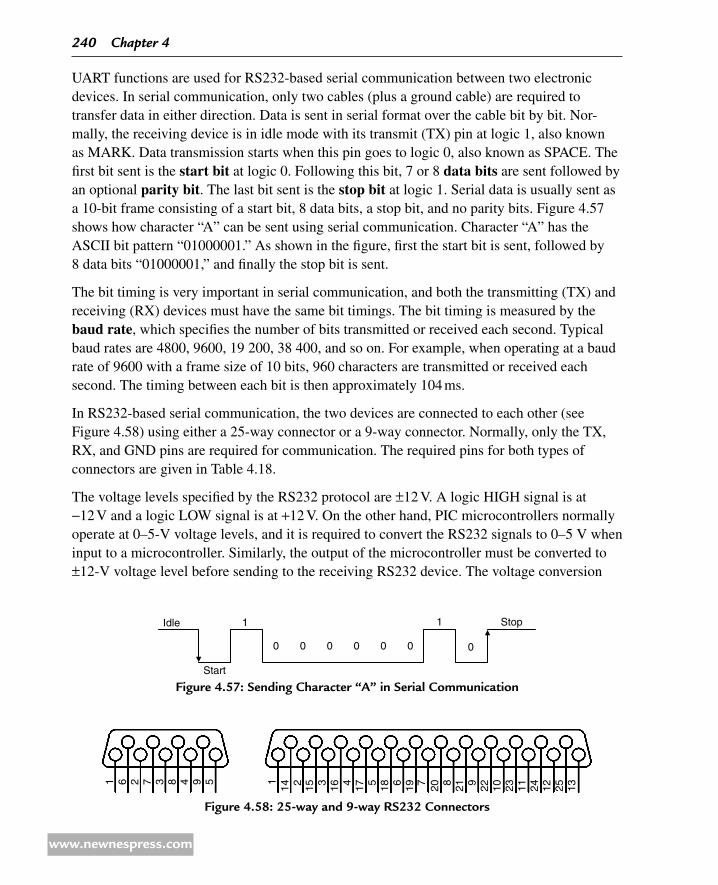
UART functions are used for RS232-based serial communication between two electronic devices. In serial communication, only two cables (plus a ground cable) are required to transfer data in either direction. Data is sent in serial format over the cable bit by bit. Nor-mally, the receiving device is in idle mode with its transmit (TX) pin at logic 1, also known as MARK. Data transmission starts when this pin goes to logic 0, also known as SPACE. The first bit sent is the start bit at logic 0. Following this bit, 7 or 8 data bits are sent followed by an optional parity bit. The last bit sent is the stop bit at logic 1. Serial data is usually sent as a 10-bit frame consisting of a start bit, 8 data bits, a stop bit, and no parity bits. Figure 4.57 shows how character “A” can be sent using serial communication. Character “A” has the ASCII bit pattern “01000001.” As shown in the figure, first the start bit is sent, followed by 8 data bits “01000001,” and finally the stop bit is sent.
The bit timing is very important in serial communication, and both the transmitting (TX) and receiving (RX) devices must have the same bit timings. The bit timing is measured by the baud rate, which specifies the number of bits transmitted or received each second. Typical baud rates are 4800, 9600, 19 200, 38 400, and so on. For example, when operating at a baud rate of 9600 with a frame size of 10 bits, 960 characters are transmitted or received each second. The timing between each bit is then approximately 104 ms.
In RS232-based serial communication, the two devices are connected to each other (see Figure 4.58) using either a 25-way connector or a 9-way connector. Normally, only the TX, RX, and GND pins are required for communication. The required pins for both types of connectors are given in Table 4.18.
The voltage levels specified by the RS232 protocol are ±12 V. A logic HIGH signal is at −12 V and a logic LOW signal is at +12 V. On the other hand, PIC microcontrollers normally operate at 0–5-V voltage levels, and it is required to convert the RS232 signals to 0–5 V when input to a microcontroller. Similarly, the output of the microcontroller must be converted to ±12-V voltage level before sending to the receiving RS232 device. The voltage conversion
Figure 4.57: Sending Character “a” in Serial CommunicationStart
Idle 1 1
0 0 0 0 0 0 0
Stop
Figure 4.58: 25-way and 9-way rS232 Connectors
11 6 2 7 3 8 4 9 5
14 15 3 16 4 17 5 18 6 19 7 20 8 21 9 22 10 23 11 24 12 25 132
240 Chapter 4
www.newnespress.com

is usually carried out using RS232 converter chips, such as the MAX232, manufactured by Maxim Inc.
Serial communication is either implemented in the hardware using a specific pin of a micro-controller or the required signals can be generated in the software from any required pin of a microcontroller. Hardware implementation requires either an on-chip UART (or USART) circuit or an external UART chip to be connected to the microcontroller. On the other hand, software-based UART is more commonly used and it does not require any special circuits. Serial data is generated by delay loops in the software-based UART applications. In this section, only the software-based UART functions will be described.
C18 compiler supports the software UART functions shown in Table 4.19. The header file “sw_uart.h” must be included at the beginning of a program using the software UART functions.
A brief description of the C18 software UART functions is given below.
OpenUART
This function configures the I/O pins for the software UART. The default pin configuration is as follows:
TX pin – port pin RB4 •
RX pin – port pin RB5 •
The above UART pin configurations can be modified by redefining the “equ” statements in files “writuart.asm2,” “readuart.asm,” and “openuart.asm” found in directory “c:\MCC18\src\traditional\pmc_common\sw_uart.”
Pins 9-Way Connectors 25-Way Connectors
TX 2 2
RX 3 3
GND 5 7
table 4.18: Pins required for Serial Communication
Functions descriptions
OpenUART Configures the UART I/O pins
ReadUART Reads a byte from software UART
WriteUART Writes a byte to software UART
putsUART Writes a string to software UART
table 4.19: C18 Software Uart Functions
Programming with the MPLAB C18 Compiler 241
www.newnespress.com
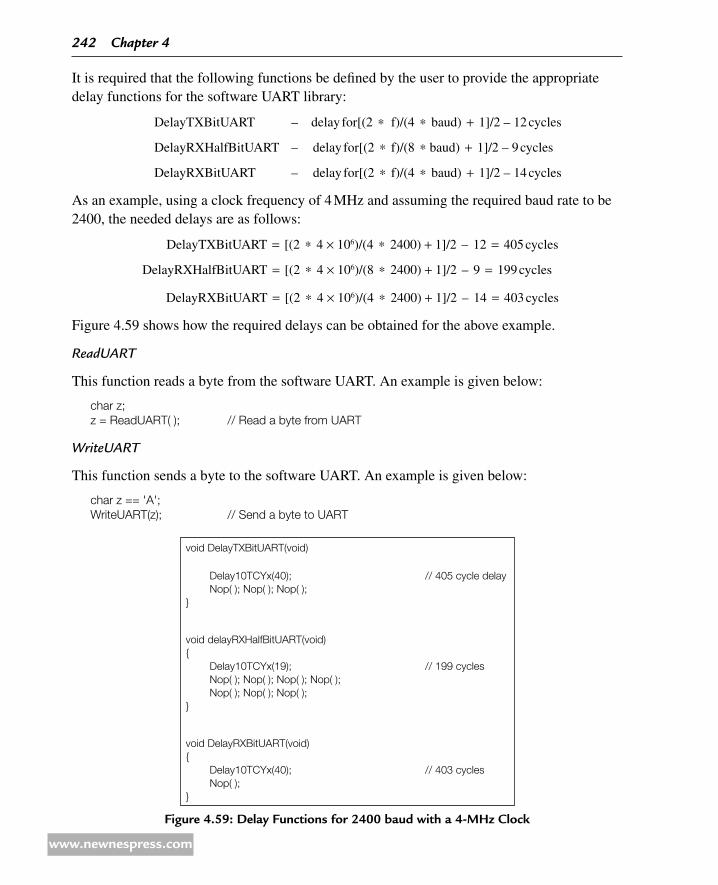
It is required that the following functions be defined by the user to provide the appropriate delay functions for the software UART library:
DelayTXBitUART – delay for[(2 * f)/(4 * baud) + 1]/2 – 12 cycles
DelayRXHalfBitUART – delay for[(2 * f)/(8 * baud) + 1]/2 – 9 cycles
DelayRXBitUART – delay for[(2 * f)/(4 * baud) + 1]/2 – 14 cycles
As an example, using a clock frequency of 4 MHz and assuming the required baud rate to be 2400, the needed delays are as follows:
DelayTXBitUART = [(2 * 4 × 106)/(4 * 2400) + 1]/2 – 12 = 405 cycles
DelayRXHalfBitUART = [(2 * 4 × 106)/(8 * 2400) + 1]/2 – 9 = 199 cycles
DelayRXBitUART = [(2 * 4 × 106)/(4 * 2400) + 1]/2 – 14 = 403 cycles
Figure 4.59 shows how the required delays can be obtained for the above example.
ReadUART
This function reads a byte from the software UART. An example is given below:
char z;z = ReadUART( ); // Read a byte from UART
WriteUART
This function sends a byte to the software UART. An example is given below:
char z == 'A';WriteUART(z); // Send a byte to UART
void DelayTXBitUART(void)
Delay10TCYx(40); // 405 cycle delayNop( ); Nop( ); Nop( );
void delayRXHalfBitUART(void)
Delay10TCYx(19); // 199 cyclesNop( ); Nop( ); Nop( ); Nop( );Nop( ); Nop( ); Nop( );
void DelayRXBitUART(void)
Delay10TCYx(40); // 403 cyclesNop( );
Figure 4.59: delay Functions for 2400 baud with a 4-Mhz Clock
242 Chapter 4
www.newnespress.com

putsUART
This function sends a string of characters to software UART. An example is given below:
char buff[ ] = "Hello World";putsUART(buff ); // Send a string to UART
example 4.33
A PIC18F452 microcontroller is connected to a PC using a MAX232 type level converter chip using the default connections as shown in Figure 4.60. Write a program to receive a character from the PC, then increment this character, and send it back to the PC. Assume that the required baud rate is 2400 and a PIC18F452 microcontroller is used with a 4-MHz crystal.
solution
The program listing is shown in Figure 4.61. The delay functions are used at the begin-ning of the program. Then, an indefinite loop is formed and a character is received from the serial line. The character is incremented by one and then sent back to the serial line.
Figure 4.60: Circuit diagram for the example 4.33
15 V
15 VVdd
Vss
OSC113
22 pF 4 MHz 22 pF
14OSC2
12
RC6RC7
252
162738495
7
6
13
T2IN
To PC
T2OUTR1I
MAX232
R1O2610
16
3
1
5
15
4
12
1mF
1mF
1mF
1mF
31
MCLRReset
PIC18F452
11
110 K 32
Programming with the MPLAB C18 Compiler 243
www.newnespress.com

/*******************************************************************************************************************************
READING AND WRITING TO SERIAL PORT ==================================
In this program PORTC pins RC6 and RC7 are configured as serial RX and TX pins respectively. The communication baud rate is set to 2400 Baud, 8 bits, no parity and with 1 stop bit.The default UART pins are TX = RB4 and RX = RB5. It is therefore necessary to modify the equ statements in the following files (found in src/traditional/pmc/sw_uart or src/extended/pmc/sw_uart) so that pins RC6 and RC7 can be used by the UART routines:
writuart.asm readuart.asm openuart.asm
The UART library should then be re-compiled using the provided batch files and then the library included in the project.
A PIC18F452 type microcontroller, operated with 4MHz is used in the design. The program receives a character from the serial port of a PC, increments this character by one, and then sends it back to the PC. Thus, for example, if character "A" is entered on the PC keyboard, character "B" will be sent back and displayed on the PC screen.
File: SERIAL.CVersion: V1.0Author: Dogan IbrahimDate: May, 2009*******************************************************************************************************************************/
#include <p18f452.h>#include <sw_uart.h>#include <delays.h>
#pragma config WDT = OFF#pragma config OSC = XT
void DelayTXBitUART(void)Delay10TCYx(40); // 405 cycle delayNop( ); Nop( ); Nop( );
void DelayRXHalfBitUART(void)
Delay10TCYx(19); // 199 cyclesNop( ); Nop( ); Nop( ); Nop( );Nop( ); Nop( ); Nop( );
void DelayRXBitUART(void)
Figure 4.61: Program Listing for example 4.33
244 Chapter 4
www.newnespress.com

Delay10TCYx(40); // 403 cyclesNop( );
//// Start of MAIN program//void main(void)
unsigned char z;
OpenUART( ); // Initialize UART
for(;;) // Endless loop
z = ReadUART( ); // Read a characterz++; // Increment characterWriteUART(z); // Write a character
Figure 4.61: Cont’d
4913 Hardware Analog-to-Digital (A/D) Converter Functions
C18 compiler provides the A/D functions shown in Table 4.20. The header file “adc.h” must be included at the beginning of a program using the A/D functions. These functions are described in this section.
BusyADC: This function checks if the A/D converter is currently performing a conversion. A logic “1” is returned when the A/D converter is ready and a logic “0” is returned if the A/D converter is not performing a conversion.
CloseADC: This function disables the A/D converter module.
ConvertADC: This function starts an A/D conversion. The function BusyADC( ) should be used to find out when the conversion is complete.
table 4.20: C18 a/d Functions
a/d Functions descriptions
BusyADC Is A/D converter busy?
CloseADC Disables the A/D converter
ConvertADC Starts an A/D conversion
OpenADC Configures the A/D converter
ReadADC Reads the conversion result
SetChanADC Selects A/D channel to be used
Programming with the MPLAB C18 Compiler 245
www.newnespress.com
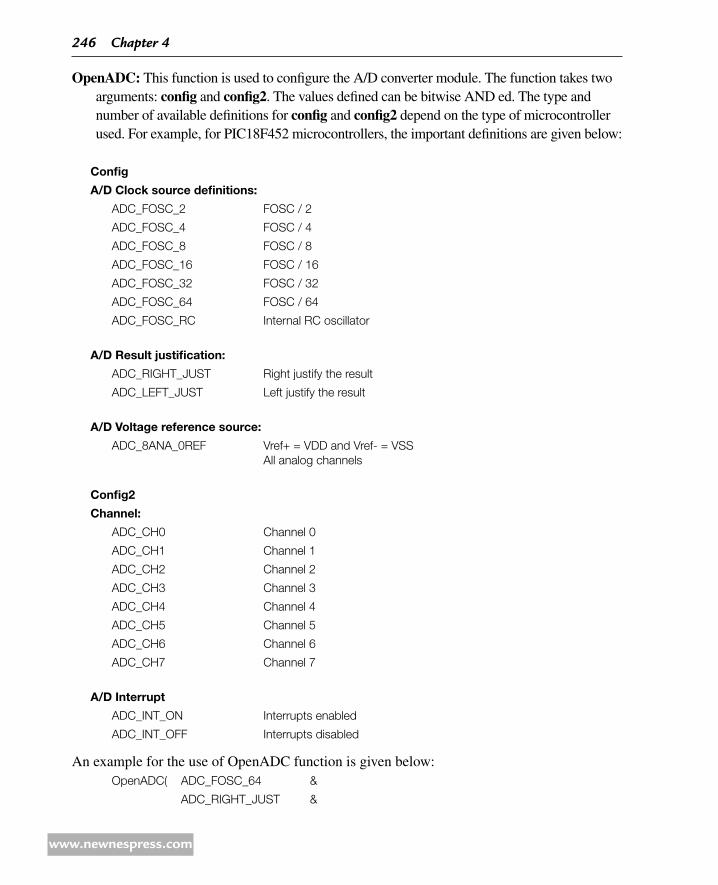
OpenADC: This function is used to configure the A/D converter module. The function takes two arguments: config and config2. The values defined can be bitwise AND ed. The type and number of available definitions for config and config2 depend on the type of microcontroller used. For example, for PIC18F452 microcontrollers, the important definitions are given below:
Config
A/D Clock source definitions:
ADC_FOSC_2 FOSC / 2
ADC_FOSC_4 FOSC / 4
ADC_FOSC_8 FOSC / 8
ADC_FOSC_16 FOSC / 16
ADC_FOSC_32 FOSC / 32
ADC_FOSC_64 FOSC / 64
ADC_FOSC_RC Internal RC oscillator
A/D Result justification:
ADC_RIGHT_JUST Right justify the result
ADC_LEFT_JUST Left justify the result
A/D Voltage reference source:
ADC_8ANA_0REF Vref+ = VDD and Vref- = VSS All analog channels
Config2
Channel:
ADC_CH0 Channel 0
ADC_CH1 Channel 1
ADC_CH2 Channel 2
ADC_CH3 Channel 3
ADC_CH4 Channel 4
ADC_CH5 Channel 5
ADC_CH6 Channel 6
ADC_CH7 Channel 7
A/D Interrupt
ADC_INT_ON Interrupts enabled
ADC_INT_OFF Interrupts disabled
An example for the use of OpenADC function is given below:OpenADC( ADC_FOSC_64 &
ADC_RIGHT_JUST &
246 Chapter 4
www.newnespress.com

ADC_8ANA_0REF &
ADC_CH0 &
ADC_INT_OFF );
ReadADC: This function reads the 16-bit result of the A/D conversion. An example is given below to show how A/D result can be read:int result;
OpenADC( ADC_FOSC_64 & ADC_RIGHT_JUST & ADC_8ANA_0REF & ADC_CH0 & ADC_INT_OFF );
ConvertADC( );while(BusyADC( )); // Wait until conversion is completeResult = ReadADC( ); // Read the A/D resultCloseADC( );
4914 Hardware Input Capture Functions
These functions are used to implement the input capture functions in hardware. More information can be obtained from the document MPLAB C18 C Compiler Libraries.
4915 Hardware I2C Functions
These functions are used to implement the I2C bus functions in hardware. More information can be obtained from the document MPLAB C18 C Compiler Libraries.
4916 Hardware I/O Port Functions
These functions are used to implement I/O port functions in hardware. More information can be obtained from the document MPLAB C18 C Compiler Libraries.
4917 Hardware Microwire Functions
These functions are used to implement the microwire bus functions in hardware. More infor-mation can be obtained from the document MPLAB C18 C Compiler Libraries.
4918 Hardware Pulse Width Modulation Functions
These functions are used to implement pulse width modulation functions in hard-ware. More information can be obtained from the document MPLAB C18 C Compiler Libraries.
Programming with the MPLAB C18 Compiler 247
www.newnespress.com

4919 Hardware sPI Functions
These functions are used to implement the SPI bus functions in hardware. More information can be obtained from the document MPLAB C18 C Compiler Libraries.
4920 Hardware Timer Functions
These functions are used to configure the microcontroller timers. The header file “timers.h” must be included at the beginning of a program using the timer functions. Table 4.21 gives a list of the available functions.
Only Timer 0 functions are described in this section. Further information on the functions available for other timers can be obtained from the MPLAB C18 C Compiler libraries.
CloseTimer 0: This function disables the interrupt and the specified timer.
OpenTimer 0: This function is used to enable a timer. The argument consists of a parameter called config that can be made up of a number of bitwise AND ed definitions. The following definitions are available:
ConfigEnable Timer 0 interrupt:
TIMER_INT_ON Interrupt enabledTIMER_INT_OFF Interrupt disabled
Timer width:T0_8BIT 8-bit modeT0_16BIT 16-bit mode
Clock source:T0_SOURCE_EXT External clock sourceT0_SOURCE_INT Internal clock source
External clock triggerT0_EDGE_FALL External clock on falling edgeT0_EDGE_RISE External clock on rising edge
table 4.21: C18 timer Functions
Functions descriptions
CloseTimerx Disables timer x
OpenTimerx Configures and enables timer x
ReadTimerx Reads the value of timer x
WriteTimerx Writes a value into timer x
x can be 0, 1, 2, 3, or 4 depending on device type.
248 Chapter 4
www.newnespress.com
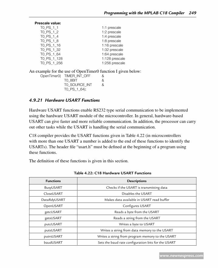
Prescale value:T0_PS_1_1 1:1 prescaleT0_PS_1_2 1:2 prescaleT0_PS_1_4 1:4 prescaleT0_PS_1_8 1:8 prescaleT0_PS_1_16 1:16 prescaleT0_PS_1_32 1:32 prescaleT0_PS_1_64 1:64 prescaleT0_PS_1_128 1:128 prescaleT0_PS_1_256 1:256 prescale
An example for the use of OpenTimer0 function I given below:OpenTimer0( TIMER_INT_OFF & T0_8BIT & T0_SOURCE_INT & T0_PS_1_64);
4921 Hardware UsART Functions
Hardware USART functions enable RS232 type serial communication to be implemented using the hardware USART module of the microcontroller. In general, hardware-based USART can give faster and more reliable communication. In addition, the processor can carry out other tasks while the USART is handling the serial communication.
C18 compiler provides the USART functions given in Table 4.22 (in microcontrollers with more than one USART a number is added to the end of these functions to identify the USARTs). The header file “usart.h” must be defined at the beginning of a program using these functions.
The definition of these functions is given in this section.
table 4.22: C18 hardware USart Functions
Functions descriptions
BusyUSART Checks if the USART is transmitting data
CloseUSART Disables the USART
DataRdyUSART Makes data available in USART read buffer
OpenUSART Configures USART
getcUSART Reads a byte from the USART
getsUSART Reads a string from the USART
putcUSART Writes a byte to USART
putsUSART Writes a string from data memory to the USART
putrsUSART Writes a string from program memory to the USART
baudUSART Sets the baud rate configuration bits for the USART
Programming with the MPLAB C18 Compiler 249
www.newnespress.com
BusyUSART: This function returns a “1” if the USART transmitter is busy transmitting a character. This function should be checked before sending a new byte to the USART. The function returns a “0” if the USART transmitter is idle.
CloseUSART: This function disables the USART.
DataRdyUSART: This function returns a “1” if data is available in the USART read buffer. A “0” indicates that data is not available in the read buffer.
getcUSART: This function reads a byte from the USART buffer. An example is given below:
int result;
result = getcUSART( );
getsUSART: This function reads a string of characters from the USART. This function waits and reads a specified number of characters. There is no timeout and the program will wait forever if the specified number of characters are not received. An example is given below to show how this function can be used:
char buff[20];
getsUSART(buff, 6); // Wait to receive 6 characters
OpenUSART: This function configures the USART. Two arguments are required: a configuration argument called config and an integer called spbrg, which specifies the value to be written to the baud rate generator register to determine the baud rate.
config
Interrupt on transmission:
USART_TX_INT_ON Transmit interrupt ON
USART_TX_INT_OFF Transmit interrupt OFF
Interrupt on reception:
USART_RX_INT_ON Receive interrupt ON
USART_RX_INT_OFF Receive interrupt OFF
USART mode:
USART_ASYNCH_MODE Asynchronous mode
USART_SYNCH_MODE Synchronous mode
Transmission width:`
USART_EIGHT_BIT 8-bit transmit/receive
USART_NINE_BIT 9-bit transmit/receive
250 Chapter 4
www.newnespress.com

Slave/Master select
USART_SYNC_SLAVE Synchronous slave
USART_SYNCH+MASTER Synchronous master
Reception mode:
USART_SINGLE_RX Single reception
USART_CONT_RX Continuous reception
Baud rate:
USART_BRGH_HIGH High baud rate
USART_BRGH_LOW Low baud rate
spbrg
This is the value written onto the baud rate generator register to define the baud rate to be used. The formula for the baud rate is as follows:
For High Speed (USART_BRGH_HIGH),
Baud = FOSC/[16 * (spbrg + 1)]
or
spbrg = FOSC/(16 * baud) − 1
and
For Low Speed (USART_BRGH_LOW),
Baud = FOSC/[16 * (spbrg + 1)]
or
spbrg = FOSC/(64 * baud) −1,
where FOSC is the microcontroller clock frequency.
For example, assuming that the clock frequency is 4 MHz and the required baud rate is 960, using high-speed setting, the value to be specified as spbrg can be calculated as
spbrg = FOSC/(16 * baud) − 1 = 4 × 10⁶/(16 × 9600) − 1 = 25
Then, the OpenUSART function can be declared as follows (in this example, it is assumed that asynchronous mode is used with 9600 baud and 8 data bits):
OpenUSART(USART_TX_INT_OFF &
USART_RX_INT_OFF &
USART_ASYNCH_MODE &
Programming with the MPLAB C18 Compiler 251
www.newnespress.com

USART_EIGHT_BIT &
USART_CONT_RX &
USART_BRGH_HIGH,
25);
putcUSART: This function sends a byte to USART.
putsUSART: This function sends a string of characters to USART from the data memory. An example is given below:
putrsUSART("My Computer");
putrsUSART: This function sends a string of characters to USART from the program memory.
baudUSART: This function sets the baud rate configuration bits for enhanced USART operation. The valid arguments can be formed from bitwise AND of the following definitions:
Clock idle state:
BAUD_IDLE_CLK_HIGH Clock idle state is high level
BAUD_IDLE_CLK_LOW Clock idle state is low level
Baud rate generation:
BAUD_16_BIT_RATE 16-bit baud rate generation
BAUD_8_BIT_RATE 8-bit baud rate generation
RX pin monitoring:
BAUD_WAKEUP_ON RX pin monitored
BAUD_WAKEUP_OFF RX pin not monitored
Baud rate measurement:
BAUD_AUTO_ON Autobaud rate measurement enabled
BAUD_AUTO_OFF Autobaud rate measurement disabled
4.10 Summary
There are many commercially available C compilers. MPLAB C18 is one of the most popular C compiler used by students and by professional programmers. Student’s version of the MPLAB C18 compiler is available free of charge and can be downloaded from the Microchip Web site. The MPLAB C18 compiler has been described in detail in this chapter including the use of built-in library functions with simple examples.
252 Chapter 4
www.newnespress.com

4.11 exercises
Write a C program to set bits 0 and 7 of PORTC to logic 1.1.
Write a C program to count down continuously and send the count to PORTB.2.
Write a C program to multiply each element of a 10-element array with number 2.3.
It is required to write a C program to add two matrices 4. P and Q. Assume that the dimension of each matrix is 3 × 3 and store the result in another matrix called W.
Repeat Exercise 4, but this time multiply matrices 5. P and Q and store the product in matrix R.
What is meant by the terms “variable” and “constant”?6.
What is meant by program repetition? Describe the operation of 7. while, do-while, and for loops in C.
What is an array? Write example statements to define the following arrays:8. a) An array of 10 integersb) An array of 30 floatc) A two-dimensional array having 6 rows and 10 columns
Trace the operation of the following loops. What will be the value of variable 9. z at the end of the loops?a) unsigned char j = 0, z = 0;
while( j < 10)
z++;
j++;
b) unsigned char z = 10;
for( j = 0; j < 10; j++)z−−;
Given the following variable definitions, list the outcome of the following conditional 10. tests in terms of “true” or “false”:
unsigned int a = 10, b = 2;
if(a > 10)
if(b >= 2)
if(a == 10)
if(a > 0)
Write a program to calculate whether a number is odd or even.11.
Programming with the MPLAB C18 Compiler 253
www.newnespress.com

Determine the value of the following bitwise operations using AND, OR, and EXOR 12. operations:
Operand 1: 00010001Operand 2: 11110001
How many times does each of the following loops iterate and what is the final value of 13. the variable j in each case?
a) for( j = 0; j < 5; j++)
b) for( j = 1; j < 10; j++)
c) for( j = 0; j <= 10; j++)
d) for( j = 0; j <= 10; j += 2)
e) for( j = 10; j > 0; j −= 2)
Write a program to calculate the sum of all positive integer numbers from 1 to 100.14.
Write a program to calculate the average value of the numbers stored in an array. Assume 15. that the array is called M and it has 20 elements.
Modify the program in Exercise 15 to find the smallest and the largest values of the array. 16. Store the smallest value in variable called Sml and the largest value in variable called Lrg.
Given that f1 and f2 are both floating point variables, explain why the following test 17. expression controlling the while loop may not be safe:
do
……………
……………
while( f1 != f2);
Why would the problem not occur if both f1 and f2 were integers? How would you correct the above while loop?
What can you say about the following 18. while loop?
k = 0;
Total = 0;
while (k < 10)
Sum++;
Total += Sum;
254 Chapter 4
www.newnespress.com

What can you say about the following 19. for loop:
Cnt = 0;
for(;;)
Cnt++;
Write a function to calculate the circumference of a rectangle. The function should 20. receive the two sides of the rectangle as floating point numbers and then return the circumference as a floating point number.
Write a main program to use the function you developed in Exercise 20. Find the 21. circumference of a rectangle whose sides are 2.3 and 5.6 cm. Store the result in a floating point number called MyResult.
Write a function to convert inches to centimeters. The function should receive inches as a 22. floating point number and then calculate the equivalent centimeters.
Write a main program to use the function you developed in Exercise 22. Convert 23. 12.5 inches into centimeters and store the result in a floating point number.
An LED is connected to port pin RB0 of a PIC18F452-type microcontroller through a 24. current limiting resistor in current sinking mode. Write a program to flash the LED with 5-s intervals.
Eight LEDs are connected to PORTB of a PIC18F452-type microcontroller. Write a 25. program so that the LEDs count up in binary sequence with 1-s delay between each output.
An LED is connected to port pin RB7 of a PIC18F452 microcontroller. Write a program 26. to flash the LED such that the ON time is 5 s and the OFF time is 3 s.
A text-based LCD is connected to a PIC18F452 type microcontroller in 4-bit data mode. 27. Write a program that will display a count from 0 to 255 on the LCD with 1-s interval between each count.
Write a program to configure port pin RB2 of a PIC18F452 microcontroller as the RS232 28. serial output port. Send character “X” to this port at 4800 baud.
Port RB0 of a PIC18F452 microcontroller is configured as the RS232 serial output port. 29. Write a program to send out string “SERIAL” at 9600 baud using software USART functions.
Repeat Exercise 29 but use the hardware USART available on the microcontroller chip.30.
Programming with the MPLAB C18 Compiler 255
www.newnespress.com

This page intentionally left blank

ChaPter 5
PIC18 Microcontroller Development Tools
The development of a microcontroller-based system is a complex process. Development tools are hardware and software tools, which help the programmers to develop and test systems in a relatively short time.
Developing software and hardware for microcontroller-based systems involves the use of editors, assemblers, compilers, debuggers, simulators, emulators, and device programmers. A typical development cycle starts with writing the application program using a text editor. The program is then translated into the executable code using an assembler or a compiler. If the program consists of several modules, then these are combined together into a single appli-cation program using a linker. At this stage, any syntax errors are detected by the assembler or the compiler and have to be corrected before an executable code can be generated. In the next stage of the development cycle, a simulator can be used to test the application program without the actual hardware. Simulators can be useful to test the correctness of an algorithm or a program with limited or no input–outputs. Most of the programming and algorithmic errors can be detected and removed during the simulation. If the programmer is happy and the program seems to be working, the next stage of the development cycle is to load the executable code to the target microcontroller chip using a device programmer and then to test the overall hardware and software system. During this cycle, software and hardware tools, such as in-circuit debuggers (ICDs) or in-circuit emulators (ICEs), can be used to analyze the operation of the program and to display the variables and registers in real time with the help of breakpoints set in the program.
5.1 Software development tools
Software development tools are computer programs, and they usually run on personal computers, helping the programmer (or system developer) to create and/or modify or test application programs. Some common software development tools are
Text editors •
Assemblers/compilers •
Simulators •
257© 2010 Elsevier Ltd. All rights reserved.D.O.I.: 10.1016/B978-1-85617-719-1.00009-9

High-level language simulators •
Integrated development environments (IDEs) •
511 Text Editors
A text editor is a program that allows us to create or edit programs and text files. Windows operating system has a text editor program called Notepad. Using Notepad, we can create a new program file, modify an existing file, or display or print the contents of a file. It is important to realize that programs used for word processing, such as the Microsoft Word, cannot be used as a text editor. This is because word processing programs are not true text editors, because they embed word formatting characters, such as bold, italic, underline, and so on, inside the text.
Most assemblers and compilers come with built-in text editors. Using these editors, we can create a program and then assemble or compile it without having to exit from the editor. These editors also provide additional features, such as automatic key word highlighting, syntax check-ing, parenthesis matching, comment-line identification, and so on. Different parts of a program can be shown in different colors to make the program more readable. For example, comments can be shown in one color, key words in another color, etc. Such features help to eliminate syntax errors during the programming stage, thus speeding up the overall development process.
512 Assemblers and Compilers
Assemblers generate executable code from assembly language programs, and that generated code can then be loaded into the flash program memory of a PIC18-based microcontroller. Similarly, compilers generate executable code from high-level language programs. Some of the commonly used compilers for the PIC18 microcontrollers are BASIC, C, and Pascal.
Assembly language is used in applications where the processing speed is very critical and the microcontroller is required to respond to external and internal events in the shortest possible time. The main disadvantage of assembly language is that it is difficult to develop complex programs using it. In addition, assembly language programs cannot be maintained easily. High-level languages, on the other hand, are easier to learn, and complex programs can be developed and tested in a much shorter time. High-level programs are also maintained more easily than assembly language programs.
Discussions of programming in this book are limited to the C language. Many different C language compilers are available for developing the PIC18 microcontroller-based programs. Some of the popular ones are
CCS C (http://www.ccsinfo.com) •
Hi-Tech C (http://www.htsoft.com) •
258 Chapter 5
www.newnespress.com
MPLAB C18 C (http://www.microchip.com) •
mikroC C (http://www.mikroe.com) •
Wiz-C C (http://www.fored.co.uk) •
Although most C compilers are essentially the same, each one has its own additions or modifications to the standard language. The C compiler used in this book is the MPLAB C18, developed by Microchip Inc.
513 simulators
A simulator is a computer program that runs on a PC without any microcontroller hardware, and it simulates the behavior of the target microcontroller by interpreting the user program instructions using the target microcontroller instruction set. Simulators can display the contents of registers, memory, and the status of input–output ports of the target microcontroller as the user program is interpreted. The user can set breakpoints to stop the execution of the program at desired locations and then examine the contents of various registers at the breakpoint. In addition, the user program can be executed in a single-step mode so that the memory and registers can be examined as the program executes one instruction at a time each time a key is pressed.
Some assembler programs also contain built-in simulators to enable programmers to develop and simulate their programs before loading onto a physical microcontroller chip. Some of the popular PIC18 microcontroller tools with built-in simulators are
MPLAB IDE (http://www.microchip.com) •
Oshon Software PIC18 simulator (http://www.oshonsoft.com) •
Forest Electronics PIC18 assembler (http://www.fored.co.uk) •
514 High-Level Language simulators
High-level language simulators are also known as source-level debuggers, and like simulators, they are programs that run on a PC and locate errors in high-level programs. We can set breakpoints in high-level statements, execute the program up to the breakpoint, and then display the values of program variables, the contents of registers, and memory locations at that breakpoint.
A source-level debugger can also invoke hardware-based debugging activity using a hardware debugger device. For example, the user program on the target microcontroller can be stopped, and the values of various variables and registers can be examined.
PIC18 Microcontroller Development Tools 259
www.newnespress.com

Some high-level language compilers, including the following three, have built-in source-level debuggers:
MPLAB C18 C •
Hi-Tech PIC18 C •
MikroC C •
515 Integrated Development Environments
IDEs are powerful PC-based programs that have everything; hence, it is possible to edit, assemble, compile, link, simulate, source-level debug, and download the generated executable code to the physical microcontroller chip (using a programmer device). These programs are in the form of graphical user interface (GUI), where the user can select various options from the program without having to exit the program. IDEs can be extremely useful during the development phases of microcontroller-based systems. Most PIC18 high-level language compilers are in the form of an IDE, thus enabling the programmer to do most tasks within a single software development tool.
5.2 hardware development tools
Numerous hardware development tools are available for the PIC18 microcontrollers. Some of these products are manufactured by Microchip Inc. and some by third-party companies. The popular hardware development tools are
Development boards •
Device programmers •
ICDs •
ICE •
Breadboards •
521 Development Boards
Development boards are invaluable microcontroller development tools. Simple development boards contain just a microcontroller and the necessary clock circuitry. Some sophisticated development boards contain LEDs, LCD, push buttons, serial ports, USB port, power supply circuit, device programming hardware, and so on.
This section is a survey of various commercially available PIC18 microcontroller development boards and their specifications.
260 Chapter 5
www.newnespress.com

LAB-XUSB Experimenter Board
The LAB-XUSB Experimenter board (see Figure 5.1) is manufactured by microEngineering Labs Inc. and can be used in 40-pin PIC18-based project development. The board is available either as an assembled or as a bare board.
The board contains
40-pin ZIF socket for PIC microcontroller •
5-V regulator •
20-MHz oscillator •
• Reset button
16-switch keypad •
Two potentiometers •
Four LEDs •
Two-line by 20-character LCD module •
Speaker •
RC servo connector •
Figure 5.1: LaB-XUSB experimenter Board
PIC18 Microcontroller Development Tools 261
www.newnespress.com

RS232 interface •
USB connector •
Socket for digital-to-analog converter (device not included) •
Socket for I2C serial EEPROM (device not included) •
Socket for Dallas DS1307 real-time clock (device not included) •
Pads for Dallas DS18S20 temperature sensors (device not included) •
In-circuit programming connector •
Prototyping area for additional circuits •
PICDEM 2 Plus
The PICDEM 2 Plus kit (see Figure 5.2) is manufactured by Microchip Inc. and can be used in the development of PIC18 microcontroller-based projects.
The board contains
2 • × 16 LCD display
Piezo sounder driven by PWM signal •
Active RS 232 port •
On-board temperature sensor •
Four LEDs •
Figure 5.2: PiCdeM 2 Plus development Board
262 Chapter 5
www.newnespress.com
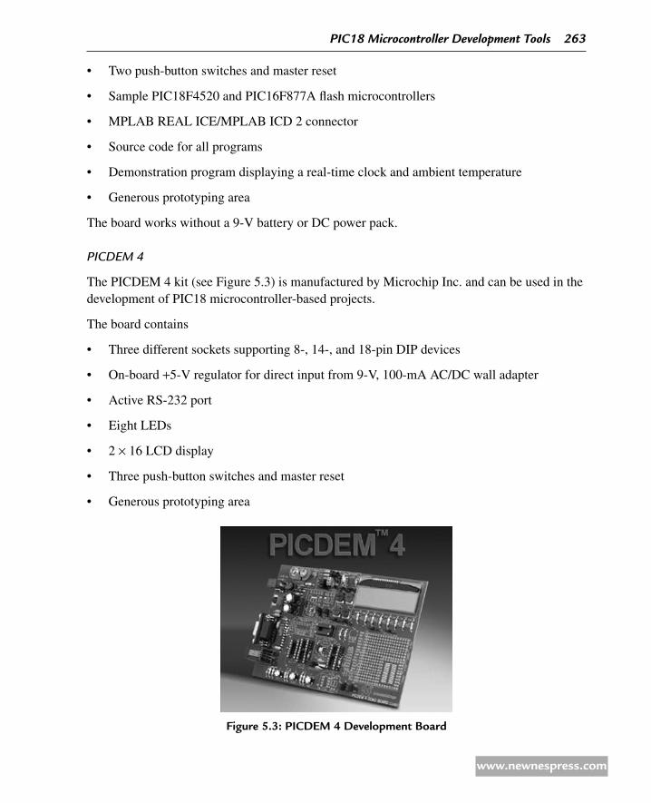
Two push-button switches and master reset •
Sample PIC18F4520 and PIC16F877A flash microcontrollers •
MPLAB REAL ICE/MPLAB ICD 2 connector •
Source code for all programs •
Demonstration program displaying a real-time clock and ambient temperature •
Generous prototyping area •
The board works without a 9-V battery or DC power pack.
PICDEM 4
The PICDEM 4 kit (see Figure 5.3) is manufactured by Microchip Inc. and can be used in the development of PIC18 microcontroller-based projects.
The board contains
Three different sockets supporting 8-, 14-, and 18-pin DIP devices •
On-board • +5-V regulator for direct input from 9-V, 100-mA AC/DC wall adapter
Active RS-232 port •
Eight LEDs •
2 • × 16 LCD display
Three push-button switches and master reset •
Generous prototyping area •
Figure 5.3: PiCdeM 4 development Board
PIC18 Microcontroller Development Tools 263
www.newnespress.com
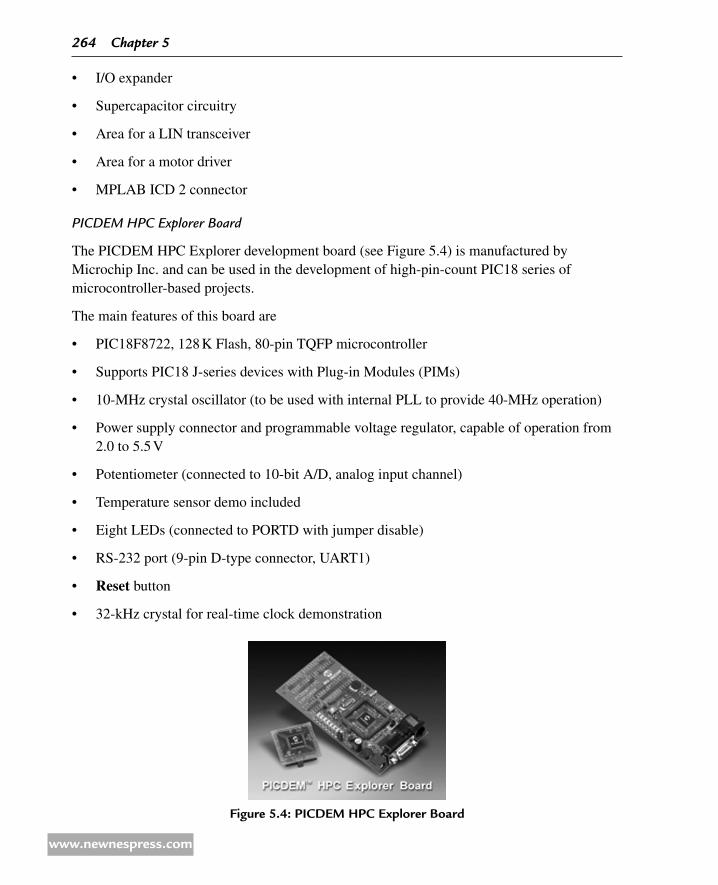
I/O expander •
Supercapacitor circuitry •
Area for a LIN transceiver •
Area for a motor driver •
MPLAB ICD 2 connector •
PICDEM HPC Explorer Board
The PICDEM HPC Explorer development board (see Figure 5.4) is manufactured by Microchip Inc. and can be used in the development of high-pin-count PIC18 series of microcontroller-based projects.
The main features of this board are
PIC18F8722, 128 K Flash, 80-pin TQFP microcontroller •
Supports PIC18 J-series devices with Plug-in Modules (PIMs) •
10-MHz crystal oscillator (to be used with internal PLL to provide 40-MHz operation) •
Power supply connector and programmable voltage regulator, capable of operation from •2.0 to 5.5 V
Potentiometer (connected to 10-bit A/D, analog input channel) •
Temperature sensor demo included •
Eight LEDs (connected to PORTD with jumper disable) •
RS-232 port (9-pin D-type connector, UART1) •
• Reset button
32-kHz crystal for real-time clock demonstration •
Figure 5.4: PiCdeM hPC explorer Board
264 Chapter 5
www.newnespress.com

MK-1 Universal PIC Development Board
The MK-1 Universal PIC development board (see Figure 5.5) is manufactured by Baji Labs and can be used for the development of the PIC microcontroller-based project with up to 40 pins. The board has a key mechanism that allows any peripheral device to be mapped to any pin of the processor, making the board very flexible. In addition, a small breadboard area is provided on the board, enabling users to design and test their own circuits.
The board has the following features
On-board selectable 3.3 or 5 V •
16 • × 2 LCD character display (8- or 4-bit mode supported)
Four-digit multiplexed 7-segment display •
10-LED bar graph (can be used as individual LEDs) •
Eight-position DIP switch •
Socketed oscillator for easy change of oscillators •
Stepper motor driver with integrated driver •
I • 2C real-time clock with crystal and battery backup support
I • 2C temperature sensor with 0.5°C precision
Figure 5.5: MK-1 Universal PiC development Board
PIC18 Microcontroller Development Tools 265
www.newnespress.com

Three potentiometers for direct A/D development •
16-button telephone keypad wired as 4 • × 4 matrix
RS232 driver with standard DB9 connector •
Socketed SPI and I • 2C EEPROM
RF Xmit and receive sockets •
IR Xmit and receive •
External drive buzzer •
Easy access to pull-up resistors •
AC adapter •
SSE452 Development Board
The SSE452 development board (see Figure 5.6), manufactured by Shuan Shizu Electronic Laboratory, can be used for developing the PIC18-based microcontroller projects, especially the PIC18FXX2 series of microcontrollers, and also for programming the microcontrollers.
The main features of this board are as follows:
One printed circuit board (PCB) suitable for any 28/40-pin PIC18 devices •
Three external interrupt pins •
Two input capture/output compare/pulse width modulation modules (CCP) •
Support for SPI, I • 2C functions
Figure 5.6: SSe452 development Board
266 Chapter 5
www.newnespress.com
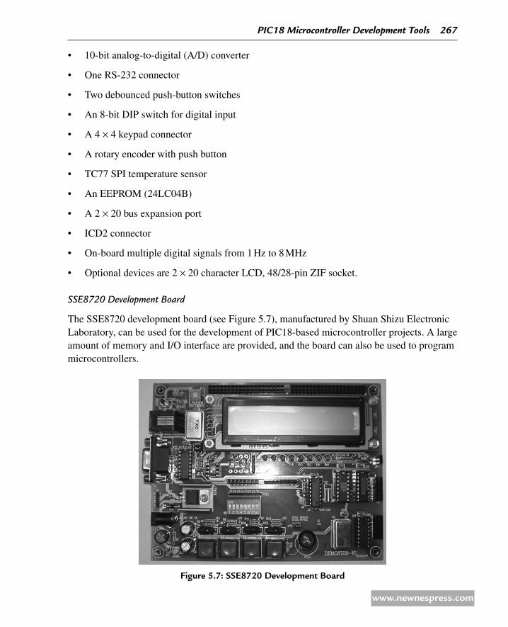
10-bit analog-to-digital (A/D) converter •
One RS-232 connector •
Two debounced push-button switches •
An 8-bit DIP switch for digital input •
A 4 • × 4 keypad connector
A rotary encoder with push button •
TC77 SPI temperature sensor •
An EEPROM (24LC04B) •
A 2 • × 20 bus expansion port
ICD2 connector •
On-board multiple digital signals from 1 Hz to 8 MHz •
Optional devices are 2 • × 20 character LCD, 48/28-pin ZIF socket.
SSE8720 Development Board
The SSE8720 development board (see Figure 5.7), manufactured by Shuan Shizu Electronic Laboratory, can be used for the development of PIC18-based microcontroller projects. A large amount of memory and I/O interface are provided, and the board can also be used to program microcontrollers.
Figure 5.7: SSe8720 development Board
PIC18 Microcontroller Development Tools 267
www.newnespress.com

The main features of this board are as follows:
20-MHz oscillator with socket •
One DB9 connector, which provides an EIA232 interface •
ICD connector •
Four debounced switches and one • Reset switch
A 4 • × 4 keypad connector
One potentiometer for experiencing A/D conversion •
Eight red LEDs •
One 8-bit DIP switch for digital inputs •
One 2 • × 20 character LCD module
24 different digital signals from 1 Hz to 16 MHz •
On-board 5-V regulator •
One I • 2C EEPROM with socket
An SPI-compatible digital temperature sensor •
An SPI-compatible real-time clock •
One CCP1 output via a NPN-transistor •
SSE8680 Development Board
The SSE8680 development board (see Figure 5.8), manufactured by Shuan Shizu Electronic Laboratory, can be used for the development of PIC18-based microcontroller projects. The board supports CAN network and a large amount of memory and an I/O interface are provided, and the board can also be used to program the microcontrollers.
The main features of this board are as follows:
20-MHz oscillator with socket •
One DB9 connector, which provides the EIA232 interface •
ICD connector •
Four debounced switches and one • Reset switch
A 4 • × 4 keypad connector
One potentiometer for experiencing A/D conversion •
268 Chapter 5
www.newnespress.com

Eight red LEDs •
One 8-bit DIP switch for digital inputs •
One 2 • × 20 character LCD module
24 different digital signals from 1 Hz to 16 MHz •
On-board 5-V regulator •
One I • 2C EPROM with socket
An SPI-compatible digital temperature sensor •
An SPI-compatible real-time clock •
One CCP1 output via an NPN transistor •
A rotary encoder •
CAN transceiver •
PIC18F4520 Development Kit
The PIC18F4520 development kit (see Figure 5.9), manufactured by Custom Computer Services Inc., includes a C compiler (PCWH), a prototyping board with the PIC18F4520 microcontroller, an ICD, and a programmer.
The main features of this development kit are
PCWH compiler •
PIC18F4520 prototyping board •
Figure 5.8: SSe8680 development Board
PIC18 Microcontroller Development Tools 269
www.newnespress.com

Breadboard area •
93LC56 serial EEPROM chip •
DS1631 digital thermometer chip •
NJU6355 real-time clock IC with attached 32.768-kHz crystal •
Two-digit 7-segment LED module •
ICD/programmer •
DC adapter and cables •
Custom Computer Services manufacture a number of other PIC18 microcontroller-based development kits and prototyping boards, such as development kits for CAN, Ethernet, Internet, USB, and serial buses. More information is available at the company's Web site.
BIGPIC4 Development Kit
The BIGPIC4 is a sophisticated development kit (Figure 5.10) that supports the latest 80-pin PIC18 family of microcontrollers. The kit is delivered already assembled, with a PIC18F8520 micro-controller installed and working at 10 MHz. The development kit includes an on-board USB port, an on-board programmer, and an ICD. The microcontroller on the board can be replaced easily.
The main features of this development kit are
46 buttons •
46 LEDs •
Figure 5.9: PiC18F4520 development Kit
270 Chapter 5
www.newnespress.com

USB connector •
External or USB power supply •
Two potentiometers •
Graphics LCD •
2 • × 16 Text LCD
MMC/SD memory card slot •
Two serial RS232 ports •
ICD •
Programmer •
PS2 connector •
Digital thermometer chip (DS1820) •
Analog inputs •
• Reset button
A new development board with the name BIGPIC5 is now available from mikroElektronika, offering most functions of the BIGPIC4 at a reduced cost and using 40-pin devices. The BIGPIC5 development board is used in some of the projects in this book.
Figure 5.10: BiGPiC4 development Kit
PIC18 Microcontroller Development Tools 271
www.newnespress.com

FUTURLEC PIC18F458 Training Board
The FUTURLEC PIC18F458 training board is a very powerful development kit (see Figure 5.11) based on the PIC18F458 microcontroller and developed by Futurlec (www.futurlec.com). The kit comes already assembled and tested. One of the biggest advantages is its low cost, which is below $45.
The main features are as follows:
PIC18F458 microcontroller with 10-MHz crystal •
RS232 communication •
Test LED •
Optional real-time clock chip with battery backup •
LCD connection •
Optional RS485/RS422 with optional chip •
CAN and SPI controller •
I • 2C expansion
In-circuit programming •
• Reset button
Speaker •
Relay socket •
All port pins available at connectors •
Figure 5.11: FUtUrLeC PiC18F458 training Board
272 Chapter 5
www.newnespress.com
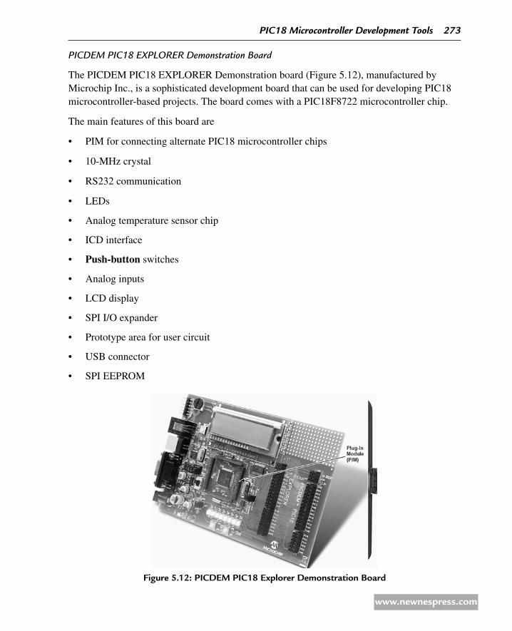
PICDEM PIC18 EXPLORER Demonstration Board
The PICDEM PIC18 EXPLORER Demonstration board (Figure 5.12), manufactured by Microchip Inc., is a sophisticated development board that can be used for developing PIC18 microcontroller-based projects. The board comes with a PIC18F8722 microcontroller chip.
The main features of this board are
PIM for connecting alternate PIC18 microcontroller chips •
10-MHz crystal •
RS232 communication •
LEDs •
Analog temperature sensor chip •
ICD interface •
• Push-button switches
Analog inputs •
LCD display •
SPI I/O expander •
Prototype area for user circuit •
USB connector •
SPI EEPROM •
Figure 5.12: PiCdeM PiC18 explorer demonstration Board
PIC18 Microcontroller Development Tools 273
www.newnespress.com

On-board voltage selection •
PICtail daughter board connector socket •
The PICDEM PIC18 Explorer Demonstration board is used in some of the projects in this book.
522 Device Programmers
After the program has been written and translated into executable code, the resulting HEX file is loaded onto the target microcontroller's program memory with the help of a device programmer. The type of device programmer depends on the type of microcontroller to be programmed. For example, some device programmers can only program PIC16 series, some can program both PIC16 and PIC18 series, and some are designed to program other models of microcontrollers (e.g., Intel 8051 series).
Some microcontroller development kits include on-board device programmers. Hence, the microcontroller chip does not need to be removed and inserted into a separate programming device. This section describes some of the popular device programmers used to program the PIC18 series of microcontrollers.
Forest Electronics USB Programmer
The USB programmer (see Figure 5.13), manufactured by Forest Electronics, can be used to program most PIC microcontrollers with up to 40 pins, including the PIC18 series. The device is connected to the USB port of a PC and receives its power from this port.
Mach X Programmer
The Mach X programmer (Figure 5.14), manufactured by Custom Computer Services Inc., can program microcontrollers of the PIC12, PIC14, PIC16, and PIC18 series ranging from
Figure 5.13: Forest electronics USB Programmer
274 Chapter 5
www.newnespress.com
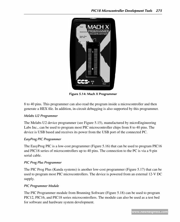
8 to 40 pins. This programmer can also read the program inside a microcontroller and then generate a HEX file. In addition, in-circuit debugging is also supported by this programmer.
Melabs U2 Programmer
The Melabs U2 device programmer (see Figure 5.15), manufactured by microEngineering Labs Inc., can be used to program most PIC microcontroller chips from 8 to 40 pins. The device is USB based and receives its power from the USB port of the connected PC.
EasyProg PIC Programmer
The EasyProg PIC is a low-cost programmer (Figure 5.16) that can be used to program PIC16 and PIC18 series of microcontrollers up to 40 pins. The connection to the PC is via a 9-pin serial cable.
PIC Prog Plus Programmer
The PIC Prog Plus (Kanda systems) is another low-cost programmer (Figure 5.17) that can be used to program most PIC microcontrollers. The device is powered from an external 12-V DC supply.
PIC Programmer Module
The PIC Programmer module from Brunning Software (Figure 5.18) can be used to program PIC12, PIC16, and PIC18 series microcontrollers. The module can also be used as a test bed for software and hardware system development.
Figure 5.14: Mach X Programmer
PIC18 Microcontroller Development Tools 275
www.newnespress.com

523 In-Circuit Debuggers
An ICD is hardware that is connected between a PC and the target microcontroller test system and is used to debug real-time applications quickly and easily. With in-circuit debugging, a monitor program runs in the PIC microcontroller in the test circuit. The programmer can set
Figure 5.15: Melabs U2 Programmer
Figure 5.16: easyProg PiC Programmer
276 Chapter 5
www.newnespress.com
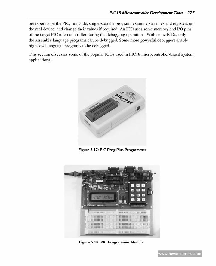
breakpoints on the PIC, run code, single-step the program, examine variables and registers on the real device, and change their values if required. An ICD uses some memory and I/O pins of the target PIC microcontroller during the debugging operations. With some ICDs, only the assembly language programs can be debugged. Some more powerful debuggers enable high-level language programs to be debugged.
This section discusses some of the popular ICDs used in PIC18 microcontroller-based system applications.
Figure 5.17: PiC Prog Plus Programmer
Figure 5.18: PiC Programmer Module
PIC18 Microcontroller Development Tools 277
www.newnespress.com

MPLAB ICD2
The MPLAB ICD2 is a low-cost ICD (see Figure 5.19) manufactured by Microchip Inc. The device can be used for debugging most PIC microcontroller-based systems. With the MPLAB, ICD2 programs are downloaded to a PIC microcontroller chip and executed in real time. This debugger supports both assembly language and C language programs. Breakpoints can be set, the microcontroller can be single-stepped, and registers and variables can be examined or changed if desired.
The MPLAB ICD 2 is connected to the PC using either a serial RS232 interface or via USB. The device acts like an intelligent interface between the PC and the test system, allowing the programmer to set breakpoints, look into the test system, view registers at breakpoints, and single-step through the user program. It can also be used to program the target PIC microcontroller.
ICD-U40
The ICD-U40 is an ICD (see Figure 5.20) manufactured by Custom Computer Services Inc. to debug programs developed with their CCS C compiler. The device operates with a 40-MHz clock frequency and is connected to the PC via the USB interface. The ICD-U40 is powered from the USB port. The company also manufactures a serial port version of this debugger called ICD-S40, which is powered from the target test system.
PICFlash 2
The PICFlash-2 ICD (see Figure 5.21) is manufactured by mikroElektronika and can be used to debug programs developed in mikroBasic, mikroC, or mikroPascal languages. The device is connected to a PC through its USB interface. Power is drawn from the USB port, so the
Figure 5.19: MPLaB iCd2 in-Circuit debugger
278 Chapter 5
www.newnespress.com

debugger requires no external power supply. The PICFlash 2 ICD is included in the BIGPIC4 development kit.
MPLAB ICD3
The MPLAB ICD3 is the new ICD device from Microchip Inc. (see Figure 5.22). This is an improved version of MPLAB ICD2, supporting most microcontroller PIC series and dsPIC devices.
The MPLAB ICD3 has the following features:
Real-time debugging of almost all PIC microcontrollers •
High-speed programming interface •
Figure 5.20: iCd-U40 in-Circuit debugger
Figure 5.21: PiCFlash 2 in-Circuit debugger
PIC18 Microcontroller Development Tools 279
www.newnespress.com

Complex breakpoints and stopwatch •
Simple target microcontroller interface •
Portable, USB interface to a PC •
Standard RJ-11 interface •
Low-voltage emulation •
Low cost •
The interface and use of the ICD3 debugger device is described later in this chapter with a detailed example.
524 In-Circuit Emulators
The ICE is one of the oldest and the most powerful devices for debugging a microcontroller system. It is also the only tool that substitutes its own internal processor for the one in the target system. Like all ICDs, the emulator's primary function is target access – the ability to examine and change the contents of registers, memory, and I/O. As the ICE replaces the CPU, it generally does not require working a CPU on the target system to provide this capability. This makes the ICE by far the best tool for troubleshooting new or defective systems.
In general, each microcontroller family has its own set of ICE. For example, an ICE for the PIC16 microcontrollers cannot be used for the PIC18 microcontrollers. Because of this, to lower the costs, emulator manufacturers provide a multiboard solution to ICE. Usually, a baseboard is provided, which is common to most microcontrollers in the family. For example, the same baseboard can be used by all PIC microcontrollers. Then, probe cards are available for individual microcontrollers. When it is required to emulate a new microcontroller in the same family, it is sufficient to purchase just the probe card for the required microcontroller.
Figure 5.22: MPLaB iCd3 in-Circuit debugger
280 Chapter 5
www.newnespress.com

Although ICEs are very powerful debugging tools, their cost is usually very high. Several models of ICEs are available on the market. The following four are some of the more popular ones.
MPLAB ICE 4000
The MPLAB ICE 4000 (Figure 5.23), manufactured by Microchip Inc., can be used to emulate microcontrollers in the PIC18 series. It consists of an emulator pod and the device adapters for the required microcontroller, which are connected using a flex cable. The pod is connected to the PC via its parallel port or using the USB port. Users can insert an unlimited number of breakpoints and examine the register values.
RICE3000
RICE3000 is a powerful ICE (Figure 5.24), manufactured by Smart Communications Ltd, for the PIC16 and PIC18 series of microcontrollers. The device consists of a base unit with different probe cards for the various members of the PIC microcontroller family. The device provides full-speed, real-time emulation up to 40 MHz, supports watching floating-point variables and complex variables, such as arrays and structures, and provides source-level and symbolic debugging in assembly and high-level languages.
ICEPIC 3
The ICEPIC 3 is a modular ICE (see Figure 5.25), manufactured by RF Solutions, for the PIC12/16 and PIC18 series of microcontrollers. The emulator is connected to the PC via its USB port. The device consists of a mother board with additional daughter boards for each microcontroller type. A daughter board is connected to the target system using device adaptors. Additionally, a trace board can be added to the device to capture and analyze execution addresses, opcodes, and external memory read/writes.
Figure 5.23: MPLaB iCe 4000
PIC18 Microcontroller Development Tools 281
www.newnespress.com

PICE-MC
This is a highly sophisticated emulator (see Figure 5.26), manufactured by Phyton Inc., and supports most PIC microcontrollers. The device consists of a main board, pod, and adapters. The main board contains the emulator logic, and memory, and interface to the PC. The pod contains a slave processor, which emulates the target microcontroller. The adapters are the mechanical parts, which are physically connected to the microcontroller socket of the target
Figure 5.25: iCePiC 3 in-Circuit emulator
Figure 5.24: riCe3000 in-Circuit emulator
282 Chapter 5
www.newnespress.com

system. PICE-MC provides source-level debugging of programs written in assembly and high-level languages. A large memory is provided on the system to capture target system data. The user can set up a large number of breakpoints and can access the program and data memories to display or change their contents.
525 Breadboards
Building an electronic circuit requires connecting the components as shown in the relevant circuit diagram, usually by soldering the components together on a strip board or a PCB. This PCB approach is appropriate for circuits that have been tested and are functioning as desired and also when the circuit is being made permanent. However, making a PCB design for just a few applications – for instance, while still developing the circuit – is not economical.
Instead, while the circuit is still under development, the components are usually assembled on a solderless breadboard. A typical breadboard is shown in Figure 5.27. The board consists of rows and columns of spaced holes so that integrated circuits and other components can be fitted inside them. The holes have spring actions so that the component leads can be held tightly inside the holes. There are various types and sizes of breadboards depending on the complexity of the circuit to be built. The boards can be stacked together to make larger boards for very complex circuits. Figure 5.28 shows the internal connection layout of the breadboard given in Figure 5.27.
The top and bottom half parts of the breadboard are entirely separate with no connection between them. Columns 1–20 in rows A–F are connected to each other on a column basis. Similarly, rows G–L in columns 1–20 are connected to each other on a column basis. Integrated circuits are placed so that the legs on one side are on the top half of the breadboard
Figure 5.26: PiCe-MC in-Circuit emulator
PIC18 Microcontroller Development Tools 283
www.newnespress.com

1 2 3 4 5 6 7 8 9 10 11 12 13 14 15 16 17 18 19 20
AB
CD
EF
GH
IJ
KL
Figure 5.27: a typical Breadboard Layout
1 2 3 4 5 6 7 8 9 10 11 12 13 14 15 16 17 18 19 20
AB
CD
EF
GH
IJ
KL
Figure 5.28: internal Wiring of the Breadboard in Fig. 5.27
and the legs on the other side of the circuit are on the bottom half of the breadboard. The first two columns on the left of the board are usually reserved for power and earth connections. Connections between the components are usually carried out using stranded (or solid) wires plugged inside the holes to be connected.
Figure 5.29 shows picture of a breadboard holding two integrated circuits and a number of resistors and capacitors.
The nice thing about the breadboard design is that the circuit can be modified very easily and quickly and different ideas can be tested without having to solder any components. The
284 Chapter 5
www.newnespress.com
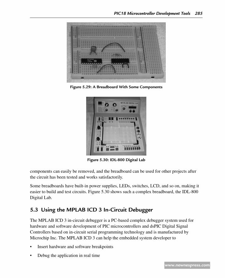
components can easily be removed, and the breadboard can be used for other projects after the circuit has been tested and works satisfactorily.
Some breadboards have built-in power supplies, LEDs, switches, LCD, and so on, making it easier to build and test circuits. Figure 5.30 shows such a complex breadboard, the IDL-800 Digital Lab.
5.3 Using the MPLaB iCd 3 in-Circuit debugger
The MPLAB ICD 3 in-circuit debugger is a PC-based complex debugger system used for hardware and software development of PIC microcontrollers and dsPIC Digital Signal Controllers based on in-circuit serial programming technology and is manufactured by Microchip Inc. The MPLAB ICD 3 can help the embedded system developer to
Insert hardware and software breakpoints •
Debug the application in real time •
Figure 5.30: idL-800 digital Lab
Figure 5.29: a Breadboard With Some Components
PIC18 Microcontroller Development Tools 285
www.newnespress.com
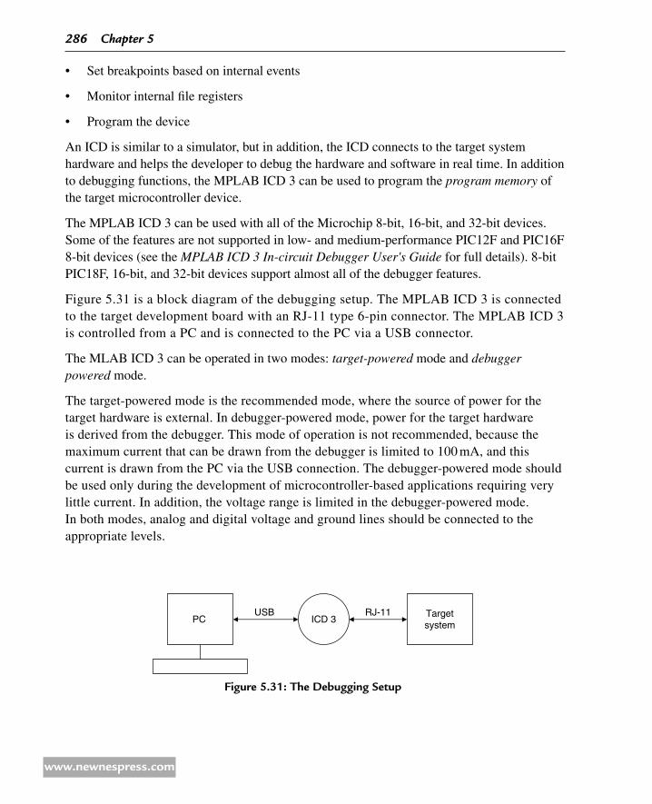
Set breakpoints based on internal events •
Monitor internal file registers •
Program the device •
An ICD is similar to a simulator, but in addition, the ICD connects to the target system hardware and helps the developer to debug the hardware and software in real time. In addition to debugging functions, the MPLAB ICD 3 can be used to program the program memory of the target microcontroller device.
The MPLAB ICD 3 can be used with all of the Microchip 8-bit, 16-bit, and 32-bit devices. Some of the features are not supported in low- and medium-performance PIC12F and PIC16F 8-bit devices (see the MPLAB ICD 3 In-circuit Debugger User's Guide for full details). 8-bit PIC18F, 16-bit, and 32-bit devices support almost all of the debugger features.
Figure 5.31 is a block diagram of the debugging setup. The MPLAB ICD 3 is connected to the target development board with an RJ-11 type 6-pin connector. The MPLAB ICD 3 is controlled from a PC and is connected to the PC via a USB connector.
The MLAB ICD 3 can be operated in two modes: target-powered mode and debugger powered mode.
The target-powered mode is the recommended mode, where the source of power for the target hardware is external. In debugger-powered mode, power for the target hardware is derived from the debugger. This mode of operation is not recommended, because the maximum current that can be drawn from the debugger is limited to 100 mA, and this current is drawn from the PC via the USB connection. The debugger-powered mode should be used only during the development of microcontroller-based applications requiring very little current. In addition, the voltage range is limited in the debugger-powered mode. In both modes, analog and digital voltage and ground lines should be connected to the appropriate levels.
Figure 5.31: the debugging Setup
PC ICD 3USB RJ-11 Target
system
286 Chapter 5
www.newnespress.com

Figure 5.32 shows the standard connection of the MPLAB ICD 3 debugger to a PIC microcontroller (in some applications, a header may be required). The RJ-11 pin configuration is as follows:
MPLaB iCd 3 pin Microcontroller pin
1 Vpp/MCLR
2 Vdd
3 Vss
4 PGD
5 PGC
6 LVP (not used in most applications)
A pull-up resistor (approximately 10 K) is recommended to be connected from the Vpp/MCLR line to the Vdd so that the microcontroller can be reset by the debugger when required.
For programming the microcontroller, no clock is needed on the microcontroller because the debugger sends clock pulses on the PGC line and data on the PGD line, while placing the programming voltage on the Vpp/MCLR line.
For debugging, the target microcontroller must be fully functional, with its power supply connected and its clock running. The requirements for debugging are
The MPLAB ICD 3 debugger must be connected to a PC via its USB cable, and the PC •must be loaded with the MPLAB IDE software (version 8.15 or higher).
The MPLAB ICD 3 debugger must be connected to the target system as shown in Figure 5.32. •
An external power should be connected to the target system, and both analog and digital •power and ground lines of the microcontroller must be connected appropriately.
The microcontroller must be fully functional with a clock source (e.g., crystal, RC, •external oscillator etc.).
Figure 5.32: Standard Connection of MPLaB iCd 3 to a Microcontroller
ICD 3PGD
Microcontroller
PGC
Vpp/MCLR
Vdd
10 K
1V
3
4
5
1
2
TO PC
PIC18 Microcontroller Development Tools 287
www.newnespress.com

The microcontroller configuration words must be programmed correctly. •
Watchdog timer must be disabled. •
Code protection must be disabled. •
Table read protection must be disabled. •
LVP must be disabled. •
531 The Debugging Process
The debugging process is shown in Figure 5.33. The debugger copies a small program called the Debug Executive to the target microcontroller. This executive runs like an application in the program memory and uses some of the file registers and some stack locations of the target microcontroller. The resources used by the debugger depend on the processor type, and more information can be found in the debugger user guide.
To find out whether or not an application program will run correctly, breakpoints are usually set in the target microcontroller device. The debugger sends commands via the PGC and PGD pins to set and store breakpoint addresses in the internal debug registers area of the target microcontroller.
The user application program starts to run from reset vector (address 0) of the program memory and will execute until a breakpoint address is encountered. At this point, control is transferred to the debug executive, and the user application program is halted. The MPLAB IDE communicates using the PGC and PGD pins of the MPLAB ICD 3 debugger and gets information about the state of the CPU and value of registers in the register file of the target microcontroller at the halted breakpoint and then displays this information on the PC as requested. The user can examine and also change the value of any register of the register file at the breakpoint if desired.
Figure 5.33: the debugging Process
ICD 3
Microcontroller
Vdd
Debugregisters
Debugexecutive
Programmemory
Fileregisters
Vpp/MCLR
PGC
PGD
288 Chapter 5
www.newnespress.com

532 The MPLAB ICD 3 Test Interface Board
A small PCB called the ICD 3 Test Interface Board is supplied with the MPLAB ICD 3 debugger device, which can be used to test that the debugger is functioning correctly. The steps to use this board are as follows:
Disconnect the debugger from the PC. •
Connect the MPLAB ICD 3 to the test interface board. •
Connect the debugger to the PC. •
Start MPLAB IDE and select ICD 3 as the programmer (or debugger). •
MPLAB IDE runs the self-test and gives a status of pass or fail. •
The MPLAB ICD 3 debugger device has three indicator lights:
Power light: • Green when debugger is connected to the PC and is receiving power via its USB cable
Active light: • Blue when power is first applied or when target is connected
Status light: • Green when the debugger is operating normally (in standby)
• Red when failed
• Orange when the debugger is busy
533 Programming with the MPLAB ICD 3 Debugger
The MPLAB ICD 3 debugger can be used to program a microcontroller. It is important to realize that all the debug features are disabled when the debugger is used as a programmer and the debug executive is not loaded into the microcontroller. The debugger can, however, toggle the MCLR line to restart the microcontroller. Clock is not required when the debugger is used as a programmer.
An example is given below.
example 5.1
Eight LEDs are connected to PORTD of a PIC18F8722 type microcontroller (any other type of PIC18 series microcontroller can be used in this example, e.g., PIC18F4520) operating with a 10-MHz clock frequency (see Figure 5.34). Write a program to flash the LEDs on and off five times with 1-s delay between each flashing.
PIC18 Microcontroller Development Tools 289
www.newnespress.com

solution
Although the circuit can be built on a breadboard, in this example, the PICDEM 18 Explorer Development board is used for simplicity. This board is based on the PIC18F8722 80-pin microcontroller and has eight LEDs connected to PORTD of the microcontroller, and the board is compatible with the MPLAB ICD 3 debugger, providing an RJ-11 type socket for the debugger interface.
The required program listing is shown in Figure 5.35. PORTD is configured as output and a for loop is used with variable k to flash the LEDs five times with a 1-s delay between each output. Note that the delay function delay10KtCYx(250) c reates a 250 × 10,000 cycle time delay. With a 10-MHz clock frequency, the clock period is 0.1 μs, and the cycle time is 0.4 μs. Thus, 2,500,000 cycle delay is equivalent to 2,500,000 × 0.4 μs = 1,000,000 μs or 1 s.
The steps to build and compile the program are given in detail in Section 4.3. After the successful compilation, the steps to program the microcontroller with the MPLAB ICD 3 debugger are as follows:
Connect the MPLAB ICD 3 to the target board (or to the PICDEM 18 Explorer • Development board) via the RJ-11 connector.
If using the PICDEM 18 Explorer Development board, set the following: •
Switch S4 to PIC MCU. •
Place jumper JP1 to enable LEDs. •
Figure 5.34: Circuit diagram of example 5.1
ICD 33
4 52
63 390
64
65
66
67
68
69
72
MCLRRD7
LED
15 V
Vdd
RD6
RD5
RD4
RD3
RD2
RD1
RD0
PIC18F8722
OSC1 OSC2
PGC/RB6
PGD/RB7
Vss
9
12 32 48 71
47
11
5170
49 50
22 nF 22 nF10 MHz
31
5
1 10 K
2
290 Chapter 5
www.newnespress.com

Connect the MPLAB ICD 3 to the PC via the USB cable. •
Connect • +5-V power supply to the target board (or 9–12-V supply to the PICDEM 18 Explorer Development board).
Select the MPLAB ICD 3 programmer. • Programmer -> Select Programmer -> MPLaB iCd 3.
Select • Project -> Build Configuration -> release.
Select • Project -> Build all to rebuild the project in Release mode.
/*****************************************************************************************************************************************
FLASHING LEDs =============
This program flashes 8 LEDs connected to PortD of a microcontroller 5 times with 1-s intervals. C18 library function Delay10KTCYx is used to create a 1-s delay between the flashes.
A PIC18F8722 microcontroller is used with a 10-MHz clock.
Programmer: Dogan IbrahimFile: FLASH.CVersion: 1.0Date: May, 2009*****************************************************************************************************************************************/
#include <p18f8722.h>#include <delays.h>#pragma config WDT = OFF, OSC = HS
void main(void)
unsigned char k;
TRISD = 0; // Configure PORTD as output for(k=0; k<5; k++) // Do 5 times PORTD = 0; // Turn OFF LED Delay10KTCYx(250); // 1 second delay PORTD = 0xFF; // Turn ON LED Delay10KTCYx(250); // 1 second delay
while(1); // wait here forever
Figure 5.35: Program Listing of example 5.1
PIC18 Microcontroller Development Tools 291
www.newnespress.com
Select • Programmer -> Program to program the target microcontroller. The following message will be displayed after successful programming:
Programming… •
Programming/Verify complete •
Press the • reset button to start the program. The eight LEDs connected to PORTD should flash five times with a 1-s delay between each output
534 MPLAB ICD 3 Debugging Example I
An example is given in this section to show how the MPLAB ICD 3 debugger can be used.
example 5.2
Repeat Example 5.1, but compile the program in debug mode, and use the MPLAB ICD 3 debugger to run the program in single-step mode.
solution
The circuit diagram and the program listing are as in Figures 5.34 and 5.35, respectively. The program should be compiled and run in single-step debug mode. The steps are
Select the MPLAB ICD 3 debugger. • debugger -> Select tool -> MPLaB iCd 3.
Select • Project -> Build Configuration -> debug.
Select • Project -> Build all to rebuild the project in Debug mode.
Select • debugger -> Program to load the code into the target microcontroller.
Press • F7 key several times until the C code is displayed in the debug window.
Press • F7 to single-step through the program.
Set the values of PORTD to be displayed during the debugging. Select • View -> Watch. Select PORTD and click add SFr to add PORTD to the watch window (see Figure 5.36).
When the debug cursor (green arrow) is on the Delay10KTCYx function, press • F8 to skip to the next instruction without displaying the contents of this function.
292 Chapter 5
www.newnespress.com

Press • F7 to execute the PORTD = 0xFF instruction (the LEDs will turn ON).
When the cursor is again on the Delay10KTCYx function, press • F8 to skip to the next instruction without displaying the contents of this function.
Repeat the above sequence as required. •
To run the program without single-stepping, press F5 to halt the program, press F6 to reset, and then press F9 to run continuously.
535 MPLAB ICD 3 Debugging Example II
This example will show how breakpoints can be used with the debugger.
example 5.3
Repeat Example 5.2, but set a breakpoint after the LEDs are turned ON and run the program up to this breakpoint.
solution
The circuit diagram and the program listing are as in Figures 5.34 and 5.35, respectively. The required steps are as follows:
Select the MPLAB ICD 3 debugger. • debugger -> Select tool -> MPLaB iCd 3.
Select • Project -> Build Configuration -> debug.
Select • Project -> Build all to rebuild the project in Debug mode.
Figure 5.36: the debug Watch Window
PIC18 Microcontroller Development Tools 293
www.newnespress.com

Select • debugger -> Program to load the code into the target microcontroller.
Set breakpoint at the delay instruction just after the LEDs are turned ON • (after the PORTD = 0xFF instruction). To do this, place the cursor on the second DelayKTCYx(250) instruction and right click the mouse. Select Set Breakpoint. A red character “B” will be inserted onto the left-hand side of the code to indicate the breakpoint (see Figure 5.37).
Run the program by pressing • F9. The program will run until the second DelayKT-CYx(250) instruction is encountered and then will halt with the green arrow pointing to the breakpoint. At this point, all the LEDs will turn ON.
Press • F5 to halt the program.
536 MPLAB ICD 3 Debugging Example III
This example will show how more than one breakpoint can be used with the debugger.
example 5.4
Repeat Example 5.3, but set two breakpoints, one before turning the LEDs ON and another after turning the LEDs ON, so that when F9 is pressed to run the program, the states of the LEDs alternate.
Figure 5.37: Setting a Breakpoint
294 Chapter 5
www.newnespress.com

Figure 5.38: Setting two Breakpoints
solution
The circuit diagram and the program listing are as in Figures 5.34 and 5.35, • respectively. The required steps are
Select the MPLAB ICD 3 debugger. • debugger -> Select tool -> MPLaB iCd 3.
Select • Project -> Build Configuration -> debug.
Select • Project -> Build all to rebuild the project in Debug mode.
Select • debugger -> Program to load the code into the target microcontroller.
Set two breakpoints, one at each delay instruction. To do this, place the cursor on •the first DelayKTCYx(250) instruction and right click the mouse. Select Set Break-point. A red character “B” will be inserted into the left-hand side of the code to indicate the breakpoint. Then, place the cursor on the second DelayKTCYx(250) instruction and right click the mouse. Select Set Breakpoint. A red character “B” will be inserted into the left-hand side of the code to indicate the breakpoint (see Figure 5.38).
Press • F9 to run the program. The LEDs will be OFF. Press F9 again, the LEDs will be ON, and repeat as necessary.
PIC18 Microcontroller Development Tools 295
www.newnespress.com

5.4 Summary
This chapter has described the PIC microcontroller software and hardware development tools. It shows that software tools like text editors, assemblers, compilers, and simulators may be required for system development. The required hardware tools include development boards/kits, programming devices, ICDs, or ICEs. In this book, the MPLAB C18 compiler is used in the examples and projects.
Steps in developing and testing MPLAB C18-based C programs are given in the chapter with and without a hardware ICD. In addition, examples of using the PICDEM 18 Explorer development board are shown with the MPLAB ICD 3 ICD.
5.5 exercises
Describe various phases of the microcontroller-based system development cycle.1.
Give a brief description of the microcontroller development tools.2.
Explain the advantages and disadvantages of assemblers and compilers.3.
Explain why a simulator can be a useful tool during the development of a 4. microcontroller-based product.
Explain in detail what a device programmer is. Give a few examples of device 5. programmers for the PIC18 series of microcontrollers.
Describe briefly the differences between in-circuit debuggers and in-circuit emulators. 6. List the advantages and disadvantages of each type of debugging tool.
Enter the following program into the MPLAB IDE, compile the program, and correct 7. syntax errors and any other errors you might have. Then, using the MPLAB IDE, simulate the operation of the program by single-stepping through the code and observe the values of various variables during the simulation.
/*============================================
A SIMPLE LED PROJECT
This program flashes the eight LEDs connected to PORTC of aPIC18F452 microcontroller.
============================================*/
void main()
TRISC = 0; //PORTC is output
www.newnespress.com
296 Chapter 5
PIC18 Microcontroller Development Tools 297
www.newnespress.com
do
PORTC = 0xFF; //Turn ON LEDs on PORTCPORTC = 0; //Turn OFF LEDs on PORTC
while(1); //Endless loop
8. Describe the steps necessary to use the MPLAB ICD 3 in-circuit debugger.
9. The following C program contains some deliberately introduced errors. Compile the program to find these errors and correct the errors.
void main()
unsigned char i,j,ki = 10;j = i + 1;
for(i = 0; i < 10; i++)
Sum = Sum + i;j++
10. The following C program contains some deliberately introduced errors. Compile the program to find these errors and correct the errors.
int add(int a, int b)
result = a + b
void main()
int p,q;p = 12;q = 10;z = add(p, q)z++;for(i = 0; i < z; i++)p++

This page intentionally left blank

299© 2010 Elsevier Ltd. All rights reserved.D.O.I.: 10.1016/B978-1-85617-719-1.00010-5
ChaPter 6
PIC18 Microcontroller MPLAB C18-Based simple Projects
In this chapter, we shall be looking at the design of simple PIC18 microcontroller-based projects using the MPLAB C18 language. Here, the idea is to familiarize ourselves with the basic interfacing techniques and also to learn how to use the various microcontroller peripheral registers. We shall be looking at the design of projects using LEDs, push-button switches, keyboards, LED arrays, sound devices, etc., and we shall be developing programs in C language using the MPLAB C18 language. The hardware will be designed on a low-cost breadboard, but development kits such as the PICDEM PIC18 Explorer Development board, BIGPIC5, or others can be used for the projects. We shall be starting with very simple projects and then moving to more complex ones. It is recommended that the reader follow the projects in the order given in the book. The following will be given for each project:
Circuit diagram •
Description of the hardware •
Algorithm description •
Program listing •
Description of the program •
Suggestions for further development •
A program’s algorithm can be described using many different graphical or text-based methods. Some of the commonly used methods are flow diagram, structure chart, and program description language (PDL). In this book, we shall be using PDL, which is basically the description of the flow of control in a program using simple English-like commands or keywords.
6.1 Program description Language
A PDL is a free-format English-like text, which describes the flow of control in a program. PDL is not a programming language, but it is a tool that helps the programmer to think about the logic of the program before the program has been developed. Commonly used PDL keywords are described below.
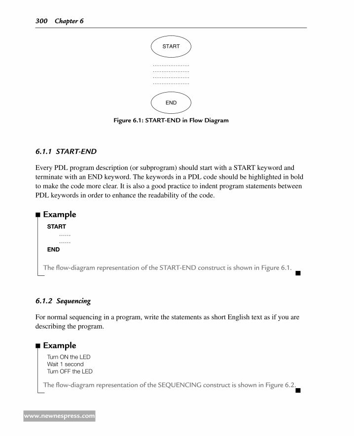
300 Chapter 6
www.newnespress.com
611 sTART-END
Every PDL program description (or subprogram) should start with a START keyword and terminate with an END keyword. The keywords in a PDL code should be highlighted in bold to make the code more clear. It is also a good practice to indent program statements between PDL keywords in order to enhance the readability of the code.
example
START…………
END
The flow-diagram representation of the START-END construct is shown in Figure 6.1.
612 sequencing
For normal sequencing in a program, write the statements as short English text as if you are describing the program.
example
Turn ON the LEDWait 1 secondTurn OFF the LED
The flow-diagram representation of the SEQUENCING construct is shown in Figure 6.2.
Figure 6.1: Start-eNd in Flow diagram
START
END
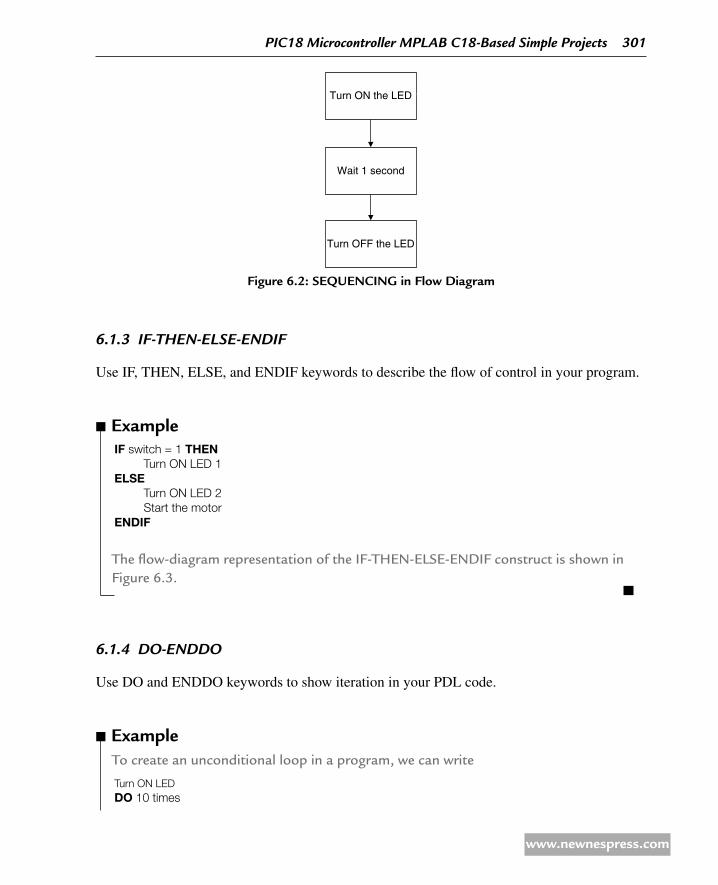
PIC18 Microcontroller MPLAB C18-Based simple Projects 301
www.newnespress.com
613 IF-THEN-ELsE-ENDIF
Use IF, THEN, ELSE, and ENDIF keywords to describe the flow of control in your program.
example
IF switch = 1 THENTurn ON LED 1
ELSETurn ON LED 2Start the motor
ENDIF
The flow-diagram representation of the IF-THEN-ELSE-ENDIF construct is shown in Figure 6.3.
614 DO-ENDDO
Use DO and ENDDO keywords to show iteration in your PDL code.
example
To create an unconditional loop in a program, we can write
Turn ON LEDDO 10 times
Figure 6.2: SeQUeNCiNG in Flow diagram
Turn ON the LED
Wait 1 second
Turn OFF the LED

302 Chapter 6
www.newnespress.com
Set clock to 1Wait for 10 msSet clock to 0
ENDDO
The flow-diagram representation of the DO-ENDDO construct is shown in Figure 6.4.
A variation of the DO-ENDDO construct is to use other keywords such as DO-FOREVER, DO-UNTIL, etc., as shown in the following examples.
example
To create a conditional loop in a program, we can write
Turn OFF buzzerIF switch = 1 THEN
DO UNTIL Port 1 = 1Turn ON LEDWait for 10 msRead Port 1
ENDDOENDIF
Figure 6.3: iF-theN-eLSe-eNdiF in Flow diagram
Switch 5 1 ?
Yes
No
Turn ON LED 1
Turn ON LED 2
Start the motor

PIC18 Microcontroller MPLAB C18-Based simple Projects 303
www.newnespress.com
or the following construct can be used when an endless loop is required:
DO FOREVERRead data from Port 1Send data to Port 2Wait for 1 s
ENDDO
615 REPEAT-UNTIL
This is another control construct, which can be used in PDL codes. An example is given below, where the program waits until a switch value is equal to 1.
Figure 6.4: dO-eNddO in Flow diagram
Set clock to 1
Turn ON LED
Wait for 10 ms
Set clock to 0
J 5 0
J 5 J 1 1
J , 10 ? Yes
No

304 Chapter 6
www.newnespress.com
example
REPEATTurn ON buzzerRead switch value
UNTIL switch = 1
Note that the REPEAT-UNTIL loop is always executed at least once and more than once if the condition at the end of the loop is not met.
The flow-diagram representation of the REPEAT-UNTIL construct is shown in Figure 6.5.
6.2 Project 1 – Chasing Leds
621 Project Description
In this project, eight LEDs are connected to PORTC of a PIC18F452-type microcontroller, and the microcontroller is operated from a 4-MHz resonator. When power is applied to the microcontroller (or when the microcontroller is reset), the LEDs turn ON alternately in an anticlockwise manner, where only one LED is ON at any time. A 1-s delay is used between each output so that the LEDs can be seen turning ON and OFF.
Figure 6.5: rePeat-UNtiL in Flow diagram
Read switch value
Turn ON buzzer
Switch 5 1 ?No
Yes

PIC18 Microcontroller MPLAB C18-Based simple Projects 305
www.newnespress.com
622 Project Hardware
The circuit diagram of the project is shown in Figure 6.6. LEDs are connected to PORTC in current-sourcing mode with eight 290- resistors. A 4-MHz resonator is connected between the OSC1 and OSC2 pins. In addition, an external Reset-push button is connected to the MCLR input to reset the microcontroller when required.
Figure 6.6: Circuit diagram of the Project
RESET
4.7 KVDD
1
31
12
13 14
4 MHz resonator
MCLR
RC015 290
290
290
290
290
290
290
290
16
17
18
23
24
25
26
PIC18F452
RC1
RC2
RC3
RC4
RC5
RC6
VSS
OSC1 OSC2
RC7
11 32
15 V

306 Chapter 6
www.newnespress.com
623 Project PDL
The PDL of this project is very simple and is given in Figure 6.7.
624 Project Program
The program is named as LED1.C, and the program listing is given in Figure 6.8. At the beginning of the program, variable J is declared as an unsigned character and is set to 1 so that when J is sent to PORTC, the first LED will turn ON. PORTC pins are then configured as outputs by setting TRISC = 0. The main program is in an endless for loop, where the LEDs are turned ON and OFF in an anticlockwise manner to give the chasing effect. Variable J is shifted left and sent to PORTC to turn the LEDs ON and OFF as required. The program checks continuously so that when LED 7 is turned ON, the next LED to be turned ON is LED 0.
The program can be compiled using the MPLAB C18 compiler. The HEX file (LED1.HEX) should be loaded to the PIC18F452 microcontroller using either an in-circuit debugger or a programming device.
Figure 6.9 shows the same program with the 1-s delay configured as a user function and called as One_Second_Delay. The modified program is called LED2.C.
625 Further Development
The project can be modified so that the LEDs chase each other in both directions. For example, if the LEDs are moving in an anticlockwise direction, the direction can be changed so that, when LED RB7 is ON, the next LED to turn ON is RB6; when RB6 is ON, the next LED is RB5; and so on. The LED flashing rate could also be modified to give a different effect to the project.
Figure 6.7: PdL of the Project
START Configure PORT C pins as output Initialise J = 1 DO FOREVER
Set PORT C = JShift left J by 1 digitIF J = 0 THEN
J = 1ENDIFWait 1 second
ENDDOEND

PIC18 Microcontroller MPLAB C18-Based simple Projects 307
www.newnespress.com
Figure 6.8: Program Listing
/***********************************************************************************************************************************************
CHASING LEDS============
In this project, 8 LEDs are connected to PORT C of a PIC18F452 microcontroller and the microcontroller is operated from a 4-MHz resonator. The program turns on the LEDs in an anticlockwise manner with a one-second delay between each output. The net result is that the LEDs seem to be chasing each other.
Programmer: Dogan IbrahimFile: LED1.CVersion: 1.0Date: June, 2009***********************************************************************************************************************************************/
#include <p18f452.h>#include <delays.h>#pragma config WDT = OFF, OSC = XT
void main(void) unsigned char J = 1;
TRISC = 0; // Configure PORT C as output
for(;;) // Endless loop PORTC = J; // Send J to PORT C Delay10KTCYx(100); // 1 second delay J = J << 1; // Shift left J if(J == 0) J = 1; // If last LED, move to first LED
/***********************************************************************************************************************************************
CHASING LEDS=============
In this project, 8 LEDs are connected to PORT C of a PIC18F452 microcontroller and the microcontroller is operated from a 4-MHz resonator. The program turns on the LEDs in an anticlockwise manner with a one-second delay between each output. The net result is that the LEDs seem to be chasing each other.
The one second delay is implemented as a user function.
Programmer: Dogan IbrahimFile: LED2.CVersion: 1.0Date: June, 2009***********************************************************************************************************************************************/
#include <p18f452.h>#include <delays.h>
Figure 6.9: Program Listing Using a User delay Function

308 Chapter 6
www.newnespress.com
6.3 Project 2 – Led dice
631 Project Description
This is a simple dice project based on LEDs, a push-button switch, and a PIC18F452 microcontrol-ler operating with a 4-MHz resonator. The block diagram of the project is shown in Figure 6.10.
As shown in Figure 6.11, the LEDs are organized so that when they turn ON, they indicate numbers as in real dice. Operation of the project is as follows: normally, the LEDs are all OFF to indicate that the system is ready to generate a new number. Pressing the switch gen-erates a random dice number between 1 and 6 and displays on the LEDs for 3 s. After 3 s, the LEDs turn OFF again.
632 Project Hardware
The circuit diagram of the project is shown in Figure 6.12. Seven LEDs representing the faces of dice are connected to PORTC of a PIC18F452 microcontroller in current-sourcing mode using 290- current-limiting resistors. A push-button switch is connected to bit 0 of PORTB (RB0) using a 4.7-K pull-up resistor. Input pin RB0 is normally at logic 1, and pressing the push-button switch forces this pin to logic 0. The MCLR input of the microcontroller is tied
#pragma config WDT = OFF, OSC = XT
void One_Second_Delay( ) Delay10KTCYx(100); // 1 second delay
void main(void) unsigned char J = 1;
TRISC = 0; // Configure PORT C as output
for(;;) // Endless loop PORTC = J; // Send J to PORT C One_Second_Delay( ); // One second delay J = J << 1; // Shift left J ¡f(J == 0) J = 1; // If last LED, move to first LED
Figure 6.9: Cont’d
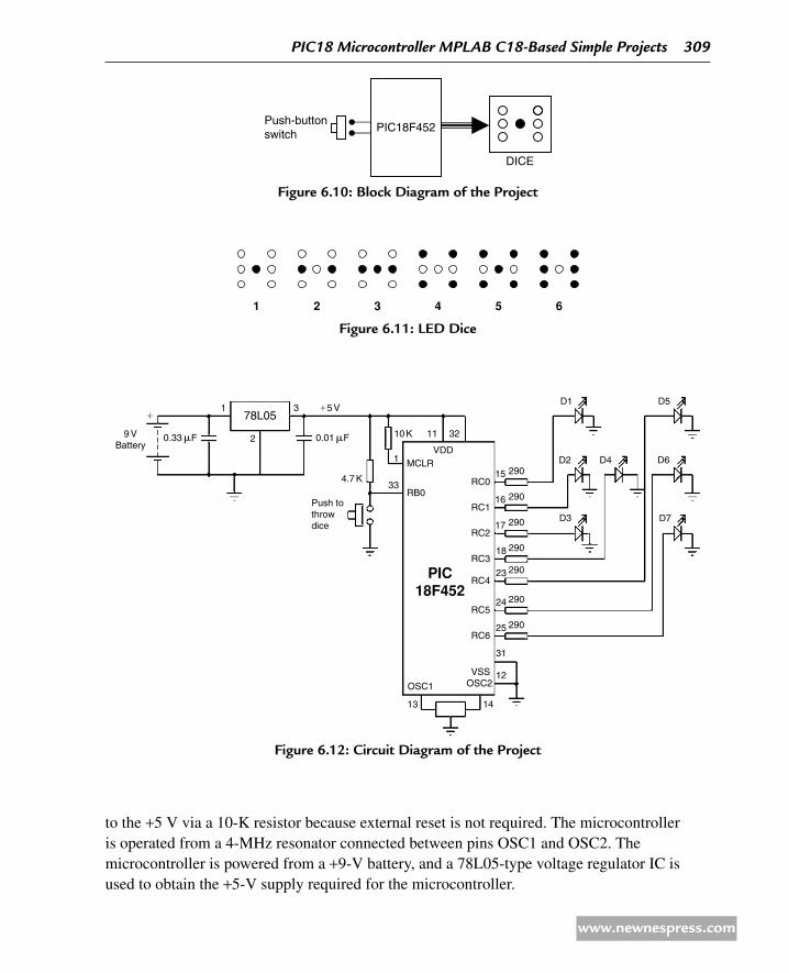
PIC18 Microcontroller MPLAB C18-Based simple Projects 309
www.newnespress.com
to the +5 V via a 10-K resistor because external reset is not required. The microcontroller is operated from a 4-MHz resonator connected between pins OSC1 and OSC2. The microcontroller is powered from a +9-V battery, and a 78L05-type voltage regulator IC is used to obtain the +5-V supply required for the microcontroller.
Figure 6.10: Block diagram of the Project
PIC18F452Push-buttonswitch
DICE
Figure 6.11: Led dice
1 2 3 4 5 6
3
33
1
10 K 11 32
MCLRVDD
RB0
OSC1
13 14
12
31
25
24
23
18
17
16
15 290
D1 D5
D6
D7
D2 D4
D3
290
290
290
290
290
290
OSC2VSS
RC6
RC5
RC4
RC3
RC2
RC1
RC0
PIC18F452
15 V
0.01 mF
4.7 K
Push tothrowdice
11
9 VBattery
0.33 mF 2
78L05
Figure 6.12: Circuit diagram of the Project

310 Chapter 6
www.newnespress.com
633 Project PDL
The operation of the project is described in the PDL given in Figure 6.13. At the begin-ning of the program, PORTC pins are configured as outputs, and bit 0 of PORTB (RB0) is configured as input. The program then executes in a loop continuously and increments a variable between 1 and 6. The state of the push-button switch is checked, and when the switch is pressed (switch output at logic 0), the current number is sent to the LEDs. A simple array is used to find out the LEDs to be turned ON corresponding to the dice number.
Table 6.1 gives the relationship between a dice number and the corresponding LEDs to be turned ON to imitate the faces of real dice. For example, to display number 1 (i.e., only the middle LED is ON), we have to turn ON D4. Similarly, to display number 4, we have to turn ON D1, D3, D5, and D7.
The relationship between the required number and the data to be sent to PORTC to turn ON the correct LEDs is given in Table 6.2. For example, to display dice number 2, we have to send hexadecimal 0x22 to PORTC. Similarly, to display number 5, we have to send hexadeci-mal 0x5D to PORTC, and so on.
634 Project Program
The program is called DICE.C, and the program listing is given in Figure 6.14. At the begin-ning of the program, PBSwitch is defined as bit 0 of PORTB, and Pressed is defined as 0.
Figure 6.13: PdL of the Project
STARTCreate DICE tableConfigure PORT C as outputsConfigure RB0 as inputSet J = 1DO FOREVER
IF button pressed THENGet LED pattern from DICE tableTurn ON required LEDsWait 3 secondsSet J = 0Turn OFF all LEDs
ENDIFIncrement JIF J = 7 THEN
Set J = 1ENDIF
ENDDOEND

PIC18 Microcontroller MPLAB C18-Based simple Projects 311
www.newnespress.com
The relationships between the dice numbers and the LEDs to be turned ON are stored in an array called DICE. Variable J is used as the dice number. Variable Pattern is the data sent to the LEDs. Program then enters an endless for loop, where the value of variable J is incre-mented very fast between 1 and 6. When the push-button switch is pressed, the LED pattern corresponding to the current value of J is read from the array and sent to the LEDs. The LEDs remain at this state for 3 s (using a variable-seconds delay function with an argument), and after this time, they all turn OFF to indicate that the system is ready to generate a new dice number.
635 Using a Pseudorandom Number Generator
In the preceding project, the value of the variable J changes very fast between 1 and 6, and when the push-button switch is pressed, the current value of this variable is taken and used as the dice number. Because the values of J are changing very fast, we can say that the numbers generated are random (i.e., new numbers do not depend on the previous numbers).
In this section, we shall see how a pseudorandom number generator function can be used to generate the dice numbers. The modified program listing (called DICE2.C) is shown
table 6.1: dice Number and Leds to be turned ON
required Number Leds to Be turned ON
1 D4
2 D2, D6
3 D2, D4, D6
4 D1, D3, D5, D7
5 D1, D3, D4, D5, D7
6 D1, D2, D3, D5, D6, D7
table 6.2: required Number and POrtC data
required Number POrtC data (hex)
1 0x08
2 0x22
3 0x2A
4 0x55
5 0x5D
6 0x77

312 Chapter 6
www.newnespress.com
Figure 6.14: Program Listing
\***********************************************************************************************************************************************
SIMPLE DICE==========
In this project, 7 LEDs are connected to PORT C of a PIC18F452 microcontroller and the microcontroller is operated from a 4-MHz resonator. The LEDs are organised as the faces of a real dice. When a push-button switch connected to RB0 is pressed, a dice pattern is displayed on the LEDs. The display remains in this state for 3 seconds and after this period the LEDs all turn OFF to indicate that the system is ready for the button to be pressed again.
Author: Dogan IbrahimDate: June 2009File: DICE.C***********************************************************************************************************************************************/
#include <p18f452.h>#include <delays.h>#pragma config WDT = OFF, OSC = XT
#define PBSwitch PORTBbits.RB0#define Pressed 0
void N_Seconds_Delay(unsigned char n)
unsigned char k;for(k=0; k<n; k++) Delay10KTCYx(100);
void main(void)
unsigned char J = 1;unsigned char Pattern;unsigned char DICE[ ] = 0,0x08,0x22,0x2A,0x55,0x5D,0x77;
TRISC = 0; // PORT C outputsTRISB = 1; // RB0 inputPORTC = 0; // Turn OFF all LEDs
for(;;) // Endless loop
if(PBSwitch == Pressed) // Is switch pressed ? Pattern = DICE[J]; // Get LED pattern PORTC = Pattern; // Turn on LEDs N_Seconds_Delay(3); // 3 seconds delay PORTC = 0; // Turn OFF all LEDs J = 0; // Initialise J
J++; // Increment Jif(J == 7) J = 1; // Back to 1 if > 6
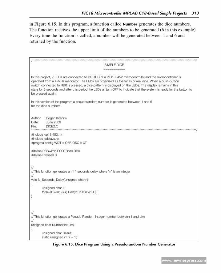
PIC18 Microcontroller MPLAB C18-Based simple Projects 313
www.newnespress.com
in Figure 6.15. In this program, a function called Number generates the dice numbers. The function receives the upper limit of the numbers to be generated (6 in this example). Every time the function is called, a number will be generated between 1 and 6 and returned by the function.
/***********************************************************************************************************************************************SIMPLE DICE
===========
In this project, 7 LEDs are connected to PORT C of a PIC18F452 microcontroller and the microcontroller is operated from a 4-MHz resonator. The LEDs are organised as the faces of real dice. When a push-button switch connected to RB0 is pressed, a dice pattern is displayed on the LEDs. The display remains in this state for 3 seconds and after this period the LEDs all turn OFF to indicate that the system is ready for the button to be pressed again.
In this version of the program a pseudorandom number is generated between 1 and 6for the dice numbers.
Author: Dogan IbrahimDate: June 2009File: DICE2.C***********************************************************************************************************************************************/#include <p18f452.h>#include <delays.h>#pragma config WDT = OFF, OSC = XT
#define PBSwitch PORTBbits.RB0#define Pressed 0
//// This function generates an “n” seconds delay where “n” is an integer//void N_Seconds_Delay(unsigned char n) unsigned char k; for(k=0; k<n; k++) Delay10KTCYx(100);
//// This function generates a Pseudo Random integer number between 1 and Lim//unsigned char Number(int Lim) unsigned char Result; static unsigned int Y = 1;
Figure 6.15: dice Program Using a Pseudorandom Number Generator

314 Chapter 6
www.newnespress.com
Y = (Y*32719 + 3) % 32749; Result = ((Y % Lim) + 1); return (Result);
//// Start of MAIN program//void main(void) unsigned char J, Pattern; unsigned char DICE[ ] = 0,0x08,0x22,0x2A,0x55,0x5D,0x77; TRISC = 0; // PORT C outputs TRISB = 1; // RB0 input PORTC = 0; // Turn OFF all LEDs for(;;) // Endless loop if(PBSwitch == Pressed) // Is switch pressed ? J = Number(6); Pattern = DICE[J]; // Get LED pattern PORTC = Pattern; // Turn on LEDs N_Seconds_Delay(3); // 3 seconds delay PORTC = 0; // Turn OFF all LEDs
The operation of the program is basically the same as in Figure 6.14. When the push-button switch is pressed, function Number is called to generate a new dice number between 1 and 6, and this number is used as an index in array DICE in order to find the bit pattern to be sent to the LEDs.
6.4 Project 3 – two-dice Project
641 Project Description
This project is similar to Project 2, but here, a pair of dice are used instead of just one. In many dice games, such as backgammon, a pair of dice are thrown together and then the player takes the action based on the outcome.
The circuit given in Figure 6.12 can be modified by adding another set of seven LEDs for the second dice. For example, the first set of LEDs can be driven from PORTC, the second set from PORTD, and the push-button switch can be connected to RB0 as before. Such a design
Figure 6.15: Cont’d

PIC18 Microcontroller MPLAB C18-Based simple Projects 315
www.newnespress.com
will require the use of 14 output ports just for the LEDs. Later on, we will see how the LEDs can be combined in order to reduce the I/O requirements. Figure 6.16 shows the block dia-gram of the project.
642 Project Hardware
The circuit diagram of the project is shown in Figure 6.17. The circuit is basically the same as Figure 6.12, with the addition of another set of LEDs connected to PORTD.
Figure 6.16: Block diagram of the Project
PIC18F452Push-buttonswitch
DICE
Figure 6.17: Circuit diagram of the Project
Push tothrowdice
D5
D6
D7
D4 D2
D3
D1
4.7 K
290 19
331
10 K 11 32VDD
15 V
MCLRRB0
RD0
OSC1 OSC2
13 14
4 MHz resonator
VSS
RC015 290
D1
D2
D3
D4
D5
D6
D7
290
290
290
290
290
290
16
17
18
23
24
25
31
12
PIC18F452
290 20
290 21
290 22
290 27
290 28
290 29
RD1
RD2
RD3
RD4
RD5
RD6
RC1
RC2
RC3
RC4
RC5
RC6

316 Chapter 6
www.newnespress.com
START Create DICE table Configure PORT C as outputs Configure PORT D as outputs Configure RB0 as input DO FOREVER IF button pressed THEN Get a random number between 1 and 6 Find bit pattern Turn ON LEDs on PORT C Get second random number between 1 and 6 Find bit pattern Turn ON LEDs on PORT D Wait 3 seconds Turn OFF all LEDs ENDIF ENDDOEND
Figure 6.18: PdL of the Project
643 Project PDL
The operation of the project is very similar to that of Project 2. Figure 6.18 shows the PDL for this project. At the beginning of the program, PORTC and PORTD pins are configured as outputs, and bit 0 of PORTB (RB0) is configured as input. The program then executes in a loop continuously and checks the state of the push-button switch. When the switch is pressed, two pseudorandom numbers are generated between 1 and 6, and these numbers are sent to PORTC and PORTD. The LEDs remain at this state for 3 s, and after this time, all the LEDs are turned OFF to indicate that the push button can be pressed again for the next pair of numbers.
644 Project Program
The program is called DICE3.C, and the program listing is given in Figure 6.19. At the begin-ning of the program, PBSwitch is defined as bit 0 of PORTB, and Pressed is defined as 0. The relationship between the dice numbers and the LEDs to be turned ON are stored in an array called DICE, as in Project 2. Variable Pattern is the data sent to the LEDs. The program enters an endless for loop, where the state of the push-button switch is checked continuously. When the switch is pressed, two random numbers are generated by calling the function Numbers twice. The bit patterns to be sent to the LEDs are then determined and sent to PORTC and PORTD to display the dice numbers. The program then repeats inside the endless loop, checking the state of the push-button switch.

PIC18 Microcontroller MPLAB C18-Based simple Projects 317
www.newnespress.com
Figure 6.19: Program Listing
/***********************************************************************************************************************************************TWO DICE
=========
In this project, 7 LEDs are connected to PORT C of a PIC18F452 microcontroller and the microcontroller is oper-ated from a 4-MHz resonator. The LEDs are organised as the faces of a real dice. When a push-button switch connected to RB0 is pressed, a dice pattern is displayed on the LEDs. The display remains in this state for 3 seconds and after this period the LEDs all turn OFF to indicate that the system is ready for the button to be pressed again.
In this version of the program, a pseudorandom number generator function is used to generate numbers between 1 and 6 for the dice numbers, and two dice are used connected to PORT C and PORT D of the microcontroller.
Author: Dogan IbrahimDate: June 2009File: DICE3.C***********************************************************************************************************************************************/#include <p18f452.h>#include <delays.h>#pragma config WDT = OFF, OSC = XT
#define PBSwitch PORTBbits.RB0#define Pressed 0
//// This function generates an “n” seconds delay where “n” is an integer//void N_Seconds_Delay(unsigned char n) unsigned char k; for(k=0; k<n; k++) Delay10KTCYx(100);
//// This function generates a Pseudo Random integer number between 1 and Lim//unsigned char Number(int Lim) unsigned char Result; static unsigned int Y = 1;
Y = (Y*32719 + 3) % 32749; Result = ((Y % Lim) + 1); return (Result);

318 Chapter 6
www.newnespress.com
6.5 Project 4 – two dice Project – Fewer i/O Pins
651 Project Description
This project is similar to Project 3, but here LEDs are shared and fewer I/O pins are used.
The LEDs in Table 6.1 can be grouped as shown in Table 6.3, and looking at this table, we can say that
D4 can appear on its own. •
D2 and D6 are always together. •
D1 and D3 are always together. •
D5 and D7 are always together. •
//// Start of MAIN program//void main(void) unsigned char J, Pattern; unsigned char DICE[ ] = 0,0x08,0x22,0x2A,0x55,0x5D,0x77; TRISC = 0; // PORT C outputs TRISD = 0; // PORT D outputs TRISB = 1; // RB0 input PORTC = 0; // Turn OFF all LEDs PORTD = 0; // Turn OFF all LEDs for(;;) // Endless loop if(PBSwitch == Pressed) // Is switch pressed ? J = Number(6); // Generate first number Pattern = DICE[J]; // Get LED pattern PORTC = Pattern; // Turn ON first LEDs J = Number(6); // Generate second number Pattern = DICE[J]; // Get LED pattern PORTD = Pattern; // Turn ON second LED N_Seconds_Delay(3); // 3 seconds delay PORTC = 0; // Turn OFF all LEDs PORTD = 0; // Turn OFF all LEDs
Figure 6.19: Cont’d

PIC18 Microcontroller MPLAB C18-Based simple Projects 319
www.newnespress.com
Thus, we can drive D4 on its own and then drive the D2, D6 pair together in series, the D1, D3 pair together in series, and also the D5, D7 pair together in series. (Actually, we could share D1, D3, D5, D7, but this would require 8 V to drive if the LEDs are connected in series. Connecting these LEDs in parallel will require excessive current, and a driver IC will be required.) All together, four lines will be required to drive seven LEDs. Similarly, four lines will be required to drive the second die. Thus, a pair of dice can be easily driven from an 8-bit output port.
652 Project Hardware
The circuit diagram of the project is shown in Figure 6.20. PORTC of a PIC18F452 micro-controller is used to drive the LEDs as follows:
RC0 drives D2, D6 of first • die
RC1 drives D1, D3 of first • die
RC2 drives D5, D7 of first • die
RC3 drives D4 of first • die
RC4 drives D2, D6 of second • die
RC5 drives D1, D3 of second • die
RC6 drives D5, D7 of second • die
RC7 drives D4 of second • die
Because we are driving two LEDs on some outputs, we can calculate the required value of the current-limiting resistors. Assuming that the voltage drop across each LED is 2 V, the current through the LED is 10 mA, and the output high voltage of the microcontroller is 4.85 V, the required resistors are
R = 4.85 2 2 2 2 10 = 85 Ω.
table 6.3: Grouping the Leds
required Number Leds to Be turned ON
1 D4
2 D2, D6
3 D2, D6, D4
4 D1, D3, D5, D7
5 D1, D3, D5, D7, D4
6 D2, D6, D1, D3, D5, D7

320 Chapter 6
www.newnespress.com
We will choose 100- resistors.
We now need to find the relationship between the dice numbers and the bit pattern to be sent to the LEDs for each die. Table 6.4 shows the relationship between the first dice numbers and the bit pattern to be sent to port pins RC0–RC3. Similarly, Table 6.5 shows the relationship between the second dice numbers and the bit pattern to be sent to port pins RC4–RC7.
We can now find the 8-bit number to be sent to PORTC to display both dice numbers as follows:
Get the first number from the number generator, call this P. •
Index the DICE table to find the bit pattern for low nibble, i.e., • L = DICE[P].
Get the second number from the number generator, call this P. •
Index the DICE table to the find bit pattern for high nibble, i.e., • U = DICE[P].
Multiply high nibble • by 16 and add low nibble to find the number to be sent to PORTC, i.e., R = 16 × U + L, where R is the 8-bit number to be sent to PORTC to display both the dice values.
RC015
16
17
18
23
24
25
26290
290
100
100
100
100
100
100D2 D6
D1 D3
D5 D7
D2 D6
D1 D3
D5 D7
D4
D1
D2
D3
D5
D6D4
D7
14
4 MHz resonator
13
D4
RC1
RC2
RC3
RC4
RC5
RC6
RC7
OSC1
VSS31
33
1
10 K4.7 K
Push tothrowdice
PIC18F452
11 32
12
RB0
MCLRVDD
15 V
OSC2
Figure 6.20: Circuit diagram of the Project

PIC18 Microcontroller MPLAB C18-Based simple Projects 321
www.newnespress.com
653 Project PDL
The operation of the project is very similar to that of Project 2. Figure 6.21 shows the PDL for this project. At the beginning of the program, PORTC pins are configured as outputs, and bit 0 of PORTB (RB0) is configured as input. The program then executes in a loop continuously and checks the state of the push-button switch. When the switch is pressed, two pseudorandom numbers are generated between 1 and 6, and the bit pattern to be sent to PORTC is found using the method described above. This bit pattern is then sent to PORTC to display both the dice numbers at the same time. The display shows the dice numbers for 3 s, and then, all the LEDs turn OFF to indicate that the system is waiting for the push button to be pressed again to display the next set of numbers.
654 Project Program
The program is called DICE4.C, and the program listing is given in Figure 6.22. At the beginning of the program, PBSwitch is defined as bit 0 of PORTB, and Pressed is defined as 0. The relationships between the dice numbers and the LEDs to be turned ON are stored
table 6.4: First die Bit Patterns
dice Number rC3 rC2 rC1 rC0 hex Value
1 1 0 0 0 8
2 0 0 0 1 1
3 1 0 0 1 9
4 0 1 1 0 6
5 1 1 1 0 E
6 0 1 1 1 7
table 6.5: Second die Bit Patterns
dice Number rC7 rC6 rC5 rC4 hex Value
1 1 0 0 0 8
2 0 0 0 1 1
3 1 0 0 1 9
4 0 1 1 0 6
5 1 1 1 0 E
6 0 1 1 1 7
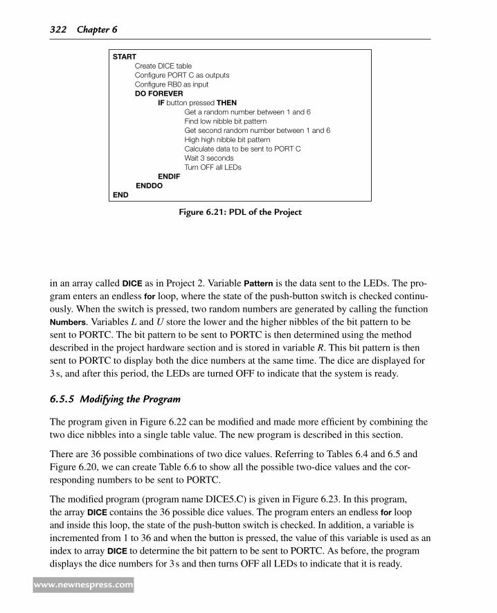
322 Chapter 6
www.newnespress.com
in an array called DICE as in Project 2. Variable Pattern is the data sent to the LEDs. The pro-gram enters an endless for loop, where the state of the push-button switch is checked continu-ously. When the switch is pressed, two random numbers are generated by calling the function Numbers. Variables L and U store the lower and the higher nibbles of the bit pattern to be sent to PORTC. The bit pattern to be sent to PORTC is then determined using the method described in the project hardware section and is stored in variable R. This bit pattern is then sent to PORTC to display both the dice numbers at the same time. The dice are displayed for 3 s, and after this period, the LEDs are turned OFF to indicate that the system is ready.
655 Modifying the Program
The program given in Figure 6.22 can be modified and made more efficient by combining the two dice nibbles into a single table value. The new program is described in this section.
There are 36 possible combinations of two dice values. Referring to Tables 6.4 and 6.5 and Figure 6.20, we can create Table 6.6 to show all the possible two-dice values and the cor-responding numbers to be sent to PORTC.
The modified program (program name DICE5.C) is given in Figure 6.23. In this program, the array DICE contains the 36 possible dice values. The program enters an endless for loop and inside this loop, the state of the push-button switch is checked. In addition, a variable is incremented from 1 to 36 and when the button is pressed, the value of this variable is used as an index to array DICE to determine the bit pattern to be sent to PORTC. As before, the program displays the dice numbers for 3 s and then turns OFF all LEDs to indicate that it is ready.
START Create DICE table Configure PORT C as outputs Configure RB0 as input DO FOREVER IF button pressed THEN Get a random number between 1 and 6 Find low nibble bit pattern Get second random number between 1 and 6 High high nibble bit pattern Calculate data to be sent to PORT C Wait 3 seconds Turn OFF all LEDs ENDIF ENDDOEND
Figure 6.21: PdL of the Project

PIC18 Microcontroller MPLAB C18-Based simple Projects 323
www.newnespress.com
/***********************************************************************************************************************************************TWO DICE - USING FEWER I/O PINS===========================
In this project, LEDs are connected to PORT C of a PIC18F452 microcontroller and the microcontroller is operated from a 4-MHz resonator. The LEDs are organised as the faces of real dice. When a push-button switch connected to RB0 is pressed, a dice pattern is displayed on the LEDs. The display remains in this state for 3 seconds and after this period the LEDs all turn OFF to indicate that the system is ready for the button to be pressed again.
In this version of the program, a pseudorandom number generator function us used to generate numbers between 1 and 6 for the dice numbers.
Author: Dogan IbrahimDate: June 2009File: DICE4.C***********************************************************************************************************************************************/#include <p18f452.h>#include <delays.h>#pragma config WDT = OFF, OSC = XT
#define PBSwitch PORTBbits.RB0#define Pressed 0
//// This function generates an “n” seconds delay where “n” is an integer//void N_Seconds_Delay(unsigned char n) unsigned char k; for(k=0; k<n; k++) Delay10KTCYx(100);
//// This function generates a Pseudo Random integer number between 1 and Lim//unsigned char Number(int Lim) unsigned char Result; static unsigned int Y = 1;
Y = (Y*32719 + 3) % 32749; Result = ((Y % Lim) + 1); return (Result);
//// Start of MAIN program//
Figure 6.22: Program Listing
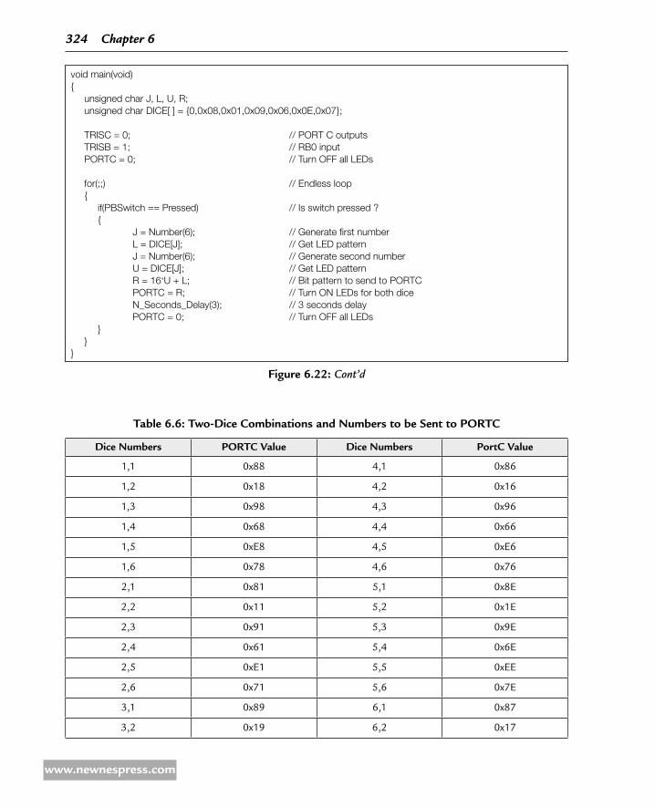
324 Chapter 6
www.newnespress.com
void main(void) unsigned char J, L, U, R; unsigned char DICE[ ] = 0,0x08,0x01,0x09,0x06,0x0E,0x07; TRISC = 0; // PORT C outputs TRISB = 1; // RB0 input PORTC = 0; // Turn OFF all LEDs for(;;) // Endless loop if(PBSwitch == Pressed) // Is switch pressed ? J = Number(6); // Generate first number L = DICE[J]; // Get LED pattern J = Number(6); // Generate second number U = DICE[J]; // Get LED pattern R = 16*U + L; // Bit pattern to send to PORTC PORTC = R; // Turn ON LEDs for both dice N_Seconds_Delay(3); // 3 seconds delay PORTC = 0; // Turn OFF all LEDs
Figure 6.22: Cont’d
table 6.6: two-dice Combinations and Numbers to be Sent to POrtC
dice Numbers POrtC Value dice Numbers PortC Value
1,1 0x88 4,1 0x86
1,2 0x18 4,2 0x16
1,3 0x98 4,3 0x96
1,4 0x68 4,4 0x66
1,5 0xE8 4,5 0xE6
1,6 0x78 4,6 0x76
2,1 0x81 5,1 0x8E
2,2 0x11 5,2 0x1E
2,3 0x91 5,3 0x9E
2,4 0x61 5,4 0x6E
2,5 0xE1 5,5 0xEE
2,6 0x71 5,6 0x7E
3,1 0x89 6,1 0x87
3,2 0x19 6,2 0x17

PIC18 Microcontroller MPLAB C18-Based simple Projects 325
www.newnespress.com
dice Numbers POrtC Value dice Numbers PortC Value
3,3 0x99 6,3 0x97
3,4 0x69 6,4 0x67
3,5 0xE9 6,5 0xE7
3,6 0x79 6,6 0x77
table 6.6: two-dice Combinations and Numbers to be Sent to POrtC —cont’d
/**********************************************************************************************************************************************
TWO DICE - USING FEWER I/O PINS===========================
In this project, LEDs are connected to PORT C of a PIC18F452 microcontroller and the microcontroller is operated from a 4-MHz resonator. The LEDs are organised as the faces of real dice. When a push-button switch connected to RB0 is pressed, a dice pattern is displayed on the LEDs. The display remains in this state for 3 seconds and after this period the LEDs all turn OFF to indicate that the system is ready for the button to be pressed again.
In this version of the program, a pseudorandom number generator function is used to generate numbers between 1 and 6 for the dice numbers.
Author: Dogan IbrahimDate: June 2009File: DICE5.C***********************************************************************************************************************************************/#include <p18f452.h>#include <delays.h>#pragma config WDT = OFF, OSC = XT
#define PBSwitch PORTBbits.RB0#define Pressed 0
//// This function generates an “n” seconds delay where “n” is an integer//void N_Seconds_Delay(unsigned char n) unsigned char k; for(k=0; k<n; k++) Delay10KTCYx(100);
//// This function generates a Pseudo Random integer number between 1 and Lim//unsigned char Number(int Lim)
Figure 6.23: Modified Program

326 Chapter 6
www.newnespress.com
6.6 Project 5 – Seven-Segment Led Counter
661 Project Description
This project describes the design of a seven-segment LED-based counter, which counts from 0 to 9 continuously with a 1-s delay between each count. The project shows how a seven-segment LED can be interfaced and used in a PIC microcontroller project.
Seven-segment displays are used frequently in electronic circuits to show numeric or alphanumeric values. As shown in Figure 6.24, a seven-segment display basically consists of
unsigned char Result; static unsigned int Y = 1;
Y = (Y*32719 + 3) % 32749; Result = ((Y % Lim) + 1); return (Result);
//// Start of MAIN program//void main(void) unsigned char Pattern, J = 1; unsigned char DICE[ ] = 0, 0x88, 0x18, 0x98, 0x68, 0xE8, 0x78, 0x81, 0x11, 0x91, 0x61, 0xE1, 0x71, 0x89, 0x19, 0x99, 0x69, 0xE9, 0x79, 0x86, 0x16, 0x96, 0x66, 0xE6, 0x76, 0x8E, 0x1E, 0x9E, 0x6E, 0xEE, 0x7E, 0x87, 0x17, 0x97, 0x67, 0xE7, 0x77; TRISC = 0; // PORT C outputs TRISB = 1; // RB0 input PORTC = 0; // Turn OFF all LEDs
for(;;) // Endless loop if(PBSwitch == Pressed) // Is switch pressed ? Pattern = DICE[J]; // Number to send to PORTC PORTC = Pattern; // Send to PORTC N_Seconds_Delay(3); // 3 seconds delay PORTC = 0; // Turn OFF all LEDs
J++; // Increment J if(J == 37) J = 1; // If J = 37, reset to 1
Figure 6.23: Cont’d

PIC18 Microcontroller MPLAB C18-Based simple Projects 327
www.newnespress.com
Figure 6.24: Some Seven-Segment displays
seven LEDs connected so that numbers 0 to 9 and some letters can be displayed. Segments are identified by letters from a to g, and Figure 6.25 shows the segment names of a typical seven-segment display.
Figure 6.26 shows how numbers from 0 to 9 can be obtained by turning ON the different segments of the display.
Seven-segment displays are available in two different configurations: common cathode and com-
mon anode. As shown in Figure 6.27, in common cathode configuration, all the cathodes of all segment LEDs are connected together to ground. The segments are turned ON by applying the logic 1 to the required segment LED via current-limiting resistors. In common cathode configur-ation, the seven-segment LED is connected to the microcontroller in current-sourcing mode.
In a common anode configuration, the anode terminals of all the LEDs are connected together, as shown in Figure 6.28. This common point is then normally connected to the supply voltage. A segment is turned ON by connecting its cathode terminal to logic 0 via a current-limiting resistor. In common anode configuration, the seven-segment LED is connected to the microcontroller in current-sinking mode.
In this project, a Kingbright SA52-11 model red common anode seven-segment display is used. This is a 13-mm (0.52-inch) display with 10 pins, and it also has a segment LED for the decimal point. Table 6.7 shows the pin configuration of this display.
a
b
c
d
e
g
f
Figure 6.25: Segment Names of a Seven-Segment display

328 Chapter 6
www.newnespress.com
Figure 6.27: Common Cathode Seven-Segment display
1V
Figure 6.28: Common anode Seven-Segment display
Figure 6.26: displaying Numbers 0–9
662 Project Hardware
The circuit diagram of the project is shown in Figure 6.29. A PIC18F452-type microcontrol-ler is used with a 4-MHz resonator. Segments a to g of the display are connected to PORTC of the microcontroller through 290-Ω current-limiting resistors. Before driving the display, we have to know the relationship between the numbers to be displayed and the corresponding segments to be turned ON, and this is shown in Table 6.8. For example, to display number 3,
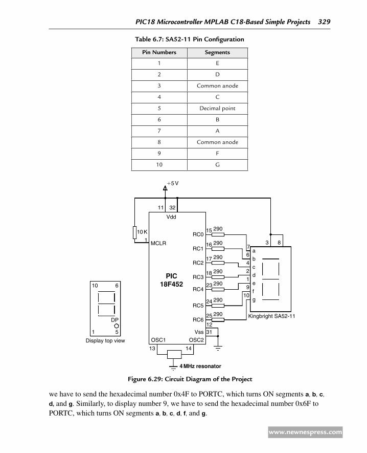
PIC18 Microcontroller MPLAB C18-Based simple Projects 329
www.newnespress.com
we have to send the hexadecimal number 0x4F to PORTC, which turns ON segments a, b, c, d, and g. Similarly, to display number 9, we have to send the hexadecimal number 0x6F to PORTC, which turns ON segments a, b, c, d, f, and g.
table 6.7: Sa52-11 Pin Configuration
Pin Numbers Segments
1 E
2 D
3 Common anode
4 C
5 Decimal point
6 B
7 A
8 Common anode
9 F
10 G
RC0
RC1
RC2
RC3
RC4
RC5
RC6
Vss
OSC2OSC1
MCLR
Vdd
15 V
11 32
15
7
6a
3 8
b
c
d
e
f
g
Kingbright SA52-11
4
2
1
9
10
290
290
290
290
290
290
290
16
17
18
23
24
25
1231
10 K
10
1
6
DP
13 14
4 MHz resonator
Display top view
5
1
PIC18F452
Figure 6.29: Circuit diagram of the Project

330 Chapter 6
www.newnespress.com
START Create SEGMENT table Configure PORT C as outputs Initialize CNT to 0 DO FOREVER Get bit pattern from SEGMENT corresponding to CNT Send this bit pattern to PORT C Increment CNT between 0 and 9 Wait 1 second ENDDOEND
Figure 6.30: PdL of the Project
table 6.8: displayed Number and data Sent to POrtC
Number x g f e d c b a POrtC data
0 0 0 1 1 1 1 1 1 0x3F
1 0 0 0 0 0 1 1 0 0x06
2 0 1 0 1 1 0 1 1 0x5B
3 0 1 0 0 1 1 1 1 0x4F
4 0 1 1 0 0 1 1 0 0x66
5 0 1 1 0 1 1 0 1 0x6D
6 0 1 1 1 1 1 0 1 0x7D
7 0 0 0 0 0 1 1 1 0x07
8 0 1 1 1 1 1 1 1 0x7F
9 0 1 1 0 1 1 1 1 0x6F
If x is not used, it is considered to be 0.
663 Project PDL
The operation of the project is shown in Figure 6.30 with a PDL. At the beginning of the program, an array called SEGMENT is declared and filled with the relationship between the numbers 0–9 and the data to be sent to PORTC. PORTC pins are then configured as outputs and a variable is initialized to 0. The program then enters an endless loop, where the variable is incremented between 0 and 9, and the corresponding bit pattern to turn ON the appropriate segments is sent to PORTC continuously with a 1-s delay between each output.
664 Project Program
The program is called SEVEN1.C, and the listing is given in Figure 6.31. At the beginning of the program, character variables Pattern and Cnt are declared, and Cnt is cleared to 0. Then, Table 6.8 is implemented using array SEGMENT. After configuring PORTC pins as outputs,

PIC18 Microcontroller MPLAB C18-Based simple Projects 331
www.newnespress.com
Figure 6.31: Program Listing
/***********************************************************************************************************************************************7-SEGMENT DISPLAY=================
In this project, a common anode 7-segment LED display is connected to PORT C of a PIC18F452 microcontroller and the microcontroller is operated from a 4-MHz resonator. The program displays numbers 0 to 9 on the display with a one-second delay between each output.
Author: Dogan IbrahimDate: June 2009File: SEVEN1.C***********************************************************************************************************************************************/#include <p18f452.h>#include <delays.h>#pragma config WDT = OFF, OSC = XT
//// This function generates 1 second delay//void One_Second_Delay( ) Delay10KTCYx(100);
//// Start of MAIN program//void main(void) unsigned char Pattern, Cnt = 0; unsigned char SEGMENT[ ] = 0x3F,0x06,0x5B,0x4F,0x66,0x6D,0x7D, 0x07,0x7F,0x6F;
TRISC = 0; // PORT C are outputs
for(;;) // Endless loop Pattern = SEGMENT[Cnt]; // Number to send to PORT C Pattern = ~Pattern; // Invert bit pattern PORTC = Pattern; // Send to PORT C Cnt++; // Increment Cnt if(Cnt == 10) Cnt = 0; // Cnt is between 0 and 9 One_Second_Delay( ); // 1 second delay
the program enters an endless loop using the for statement. Inside the loop, the bit pattern corresponding to the contents of Cnt is found and stored in variable Pattern. Because we are using a common anode display, a segment is turned ON when it is at logic 0, and thus, the bit pattern is inverted before sending to PORTC. The value of Cnt is then incremented between 0 and 9, after which the program waits for a second before repeating the above sequence.

332 Chapter 6
www.newnespress.com
Figure 6.32: Modified Program Listing
/***********************************************************************************************************************************************7-SEGMENT DISPLAY=================
In this project, a common anode 7-segment LED display is connected to PORT C of a PIC18F452 microcontroller and the microcontroller is operated from a 4-MHz resonator. The program displays numbers 0 to 9 on the display with a one-second delay between each output.
In this version of the program, a function called “Display” is used to display the number.
Author: Dogan IbrahimDate: June 2009File: SEVEN2.C***********************************************************************************************************************************************/#include <p18f452.h>#include <delays.h>#pragma config WDT = OFF, OSC = XT
//// This function generates 1 second delay//void One_Second_Delay( ) Delay10KTCYx(100);
//// This function displays a number on the 7-segment LED.// The number is passed in the argument list of the function.//unsigned char Display(unsigned char no) unsigned char Pattern; unsigned char SEGMENT[ ] = 0x3F, 0x06, 0x5B, 0x4F, 0x66, 0x6D, 0x7D, 0x07, 0x7F, 0x6F;
Pattern = SEGMENT[no]; Pattern = ~Pattern; return (Pattern);
665 Modified Program
Note that the program can be made more readable if we create a function to display the required number and then call this function from the main program. Figure 6.32 shows the modified program (called SEVEN2.C). A function called Display is created with an argument called no. The function gets the bit pattern from the local array SEGMENT indexed by no, inverts it, and then returns the resulting bit pattern to the calling program.
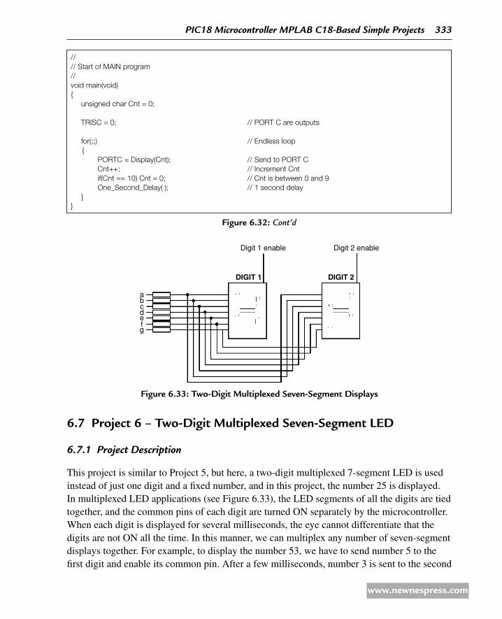
PIC18 Microcontroller MPLAB C18-Based simple Projects 333
www.newnespress.com
//// Start of MAIN program//void main(void) unsigned char Cnt = 0; TRISC = 0; // PORT C are outputs
for(;;) // Endless loop PORTC = Display(Cnt); // Send to PORT C Cnt++; // Increment Cnt if(Cnt == 10) Cnt = 0; // Cnt is between 0 and 9 One_Second_Delay( ); // 1 second delay
Figure 6.32: Cont’d
6.7 Project 6 – two-digit Multiplexed Seven-Segment Led
671 Project Description
This project is similar to Project 5, but here, a two-digit multiplexed 7-segment LED is used instead of just one digit and a fixed number, and in this project, the number 25 is displayed. In multiplexed LED applications (see Figure 6.33), the LED segments of all the digits are tied together, and the common pins of each digit are turned ON separately by the microcontroller. When each digit is displayed for several milliseconds, the eye cannot differentiate that the digits are not ON all the time. In this manner, we can multiplex any number of seven-segment displays together. For example, to display the number 53, we have to send number 5 to the first digit and enable its common pin. After a few milliseconds, number 3 is sent to the second
Digit 1 enable
DIGIT 1
abcdefg
DIGIT 2
Digit 2 enable
Figure 6.33: two-digit Multiplexed Seven-Segment displays

334 Chapter 6
www.newnespress.com
digit, and the common point of the second digit is enabled. When this process is repeated continuously, it appears to the user that both displays are ON continuously.
Some manufacturers provide multiplexed multidigit displays in single packages. For example, we can purchase 2-, 4-, or 8-digit multiplexed displays in a single package. The display used in this project is the DC56-11EWA, which is a red, 0.56-inch high common-cathode two-digit display, having 18 pins and the pin configuration shown in Table 6.9. This display can be controlled from the microcontroller as follows:
Send the segment bit pattern for digit 1 to segments • a to g.
Enable digit 1. •
Wait for a few milliseconds. •
Disable digit 1. •
Send the segment bit pattern for digit 2 to segments • a to g.
Enable digit 2. •
Wait for a few milliseconds. •
Disable digit 2. •
Repeat the above process continuously. •
The segment configuration of DC56-11EWA display is shown in Figure 6.34. In a multi-plexed display application, the segment pins of the corresponding segments are connected
table 6.9: Pin Configuration of dC56-11eWa dual display
Pin Nos. Segments
1,5 E
2,6 D
3,8 C
14 Digit 1 Enable
17,7 G
15,10 B
16,11 A
18,12 F
13 Digit 2 Enable
4 Decimal Point1
9 Decimal Point 2

PIC18 Microcontroller MPLAB C18-Based simple Projects 335
www.newnespress.com
together. For example, pins 11 and 16 are connected as a common a segment. Similarly, pins 15 and 10 are connected as a common b segment, and so on.
672 Project Hardware
The block diagram of this project is shown in Figure 6.35. The circuit diagram is given in Figure 6.36. The segments of the display are connected to PORTC of a PIC18F452-type microcontroller, operated with a 4-MHz resonator. Current-limiting resistors are used on each segment of the display. Each digit is enabled using a BC108-type transistor switch connected to the RB0 and RB1 port pins of the microcontroller. A segment is turned ON when a logic 1 is applied to the base of the corresponding segment transistor.
673 Project PDL
At the beginning of the program, PORTB and PORTC pins are configured as outputs. The program then enters an endless loop, where first the most significant digit (MSD) of the number is calculated, next function Display is called to find the bit pattern and then sent to the display, and digit 1 is enabled. Then, after a small delay, digit 1 is disabled, the least significant digit (LSD) of the number is calculated, function Display is called to find the bit pattern and then sent to the display, and digit 2 is enabled. Then, again after a small delay, digit 2 is dis-abled, and the above process repeats indefinitely. Figure 6.37 shows the PDL of the project.
PIC18F452
Enable 1
Enable 2
PORT C
PORT B
2-digit display
Figure 6.35: Block diagram of the Project
d
Enable 1
14
Enable 2
13
e f h dp1cba
16 15 3 2 1 18 17 4 11 10 8 6 5 12 7 9
d e f h dp2cba
Figure 6.34: dC56-11eWa display Segment Configuration

336 Chapter 6
www.newnespress.com
Vdd
MCLR
VSS
13
31
12
110 K
11 32
15 V
14
33 1 KBC108 BC108
DC56-11EWA common cathode
13
1 K
12
18
17
18
1
2
3
15
16 16
11
15
10
3
8
2
6
1
5
17
7
a
b
c
d
e
f
g
14
E1 E2
25
24
23
18
17
16
15 290
290
290
290
290
290
290
34
OSC1 OSC2
4 MHz resonator
RB1
RB0
PIC18F452
RC1
RC0
RC2
RC3
RC4
RC5
RC6
Figure 6.36: Circuit diagram of the Project
START Create SEGMENT table Configure PORT B as outputs Configure PORT C as outputs Initialize CNT to 25 DO FOREVER
Find MSD digitGet bit pattern from SEGMENTEnable digit 1Wait for a whileDisable digit 1Find LSD digitGet bit pattern from SEGMENTEnable digit 2Wait for a whileDisable digit 2
ENDDOEND
Figure 6.37: PdL of the Project

PIC18 Microcontroller MPLAB C18-Based simple Projects 337
www.newnespress.com
674 Project Program
The program is named SEVEN3.C, and the listing is shown in Figure 6.38. DIGIT1 and DIGIT2 are defined to be equal to bit 0 and bit 1 of PORTB, respectively. The value to be displayed (number 25) is stored in variable Cnt. An endless loop is formed using a for statement. Inside the loop, the MSD of the number is calculated by dividing the number by 10. Function Display is then called to find the bit pattern to send to PORTC. Then, digit 1 is enabled by setting DIGIT1 = 1, and the program waits for 10 ms. After this, digit 1 is disabled, and the LSD of the number is calculated using the mod operator (“%”) and sent to PORTC. At the same time, digit 2 is enabled by setting DIGIT2 = 1, and the program waits for 10 ms. After this waiting time, digit 2 is disabled and the program repeats forever.
Figure 6.38: Program Listing
/***********************************************************************************************************************************************Dual 7-SEGMENT DISPLAY
======================
In this project, two common cathode 7-segment LED displays are connected to PORT C of a PIC18F452 microcontroller and the microcontroller is operated from a 4-MHz resonator. Digit 1 (left digit) enable pin is connected to port pin RB0 and digit 2 (right digit) enable pin is connected to port pin RB1 of the microcontroller. The program displays the number 25 on the displays.
Author: Dogan IbrahimDate: June 2009File: SEVEN3.C***********************************************************************************************************************************************/#include <p18f452.h>#include <delays.h>#pragma config WDT = OFF, OSC = XT
#define DIGIT1 PORTBbits.RB0#define DIGIT2 PORTBbits.RB1
//// This function finds the bit pattern to be sent to the port to display a number// on the 7-segment LED. The number is passed in the argument list of the function.//unsigned char Display(unsigned char no) unsigned char Pattern; unsigned char SEGMENT[ ] = 0x3F,0x06,0x5B,0x4F,0x66,0x6D,0x7D,0x07, 0x7F,0x6F;
Pattern = SEGMENT[no]; // Pattern to return return (Pattern);
//// This function generates 10 ms delay//void Ten_Ms_Delay( )
338 Chapter 6
www.newnespress.com
6.8 Project 7 – two-digit Multiplexed Seven-Segment Led Counter With timer interrupt
681 Project Description
This project is similar to Project 6, but here, the timer interrupt of the microcontroller is used to refresh the displays. In Project 6, the microcontroller was busy updating the displays continuously every 10 ms, and therefore it could not perform any other tasks. For example, if we wish to make a counter with 1-s delay between each count, the program given in Project 6 cannot be used as the displays cannot be updated while the program waits for 1 s.
In this project, a counter will be designed to count from 0 to 99, and the display will be refreshed every 5 ms inside the timer interrupt service routine (ISR); the main program
Delay10KTCYx(1);
//// Start of MAIN Program//void main(void) unsigned char Msd, Lsd, Cnt = 25;
TRISC = 0; // PORT C are outputs TRISB = 0; // RB0, RB1 are outputs
DIGIT1 = 0; // Disable digit 1 DIGIT2 = 0; // Disable digit 2
for(;;) // Endless loop Msd = Cnt / 10; // MSD digit PORTC = Display(Msd); // send to PORT C DIGIT1 = 1; // Enable digit 1 Ten_Ms_Delay( ); // Wait a while
DIGIT1 = 0; // Disable digit 1 Lsd = Cnt % 10; // LSD digit PORTC = Display(Lsd); // Send to PORT C DIGIT2 = 1; // Enable digit 2 Ten_Ms_Delay( ); // Wait a while DIGIT2 = 0; // Disable digit 2
Figure 6.38: Cont’d
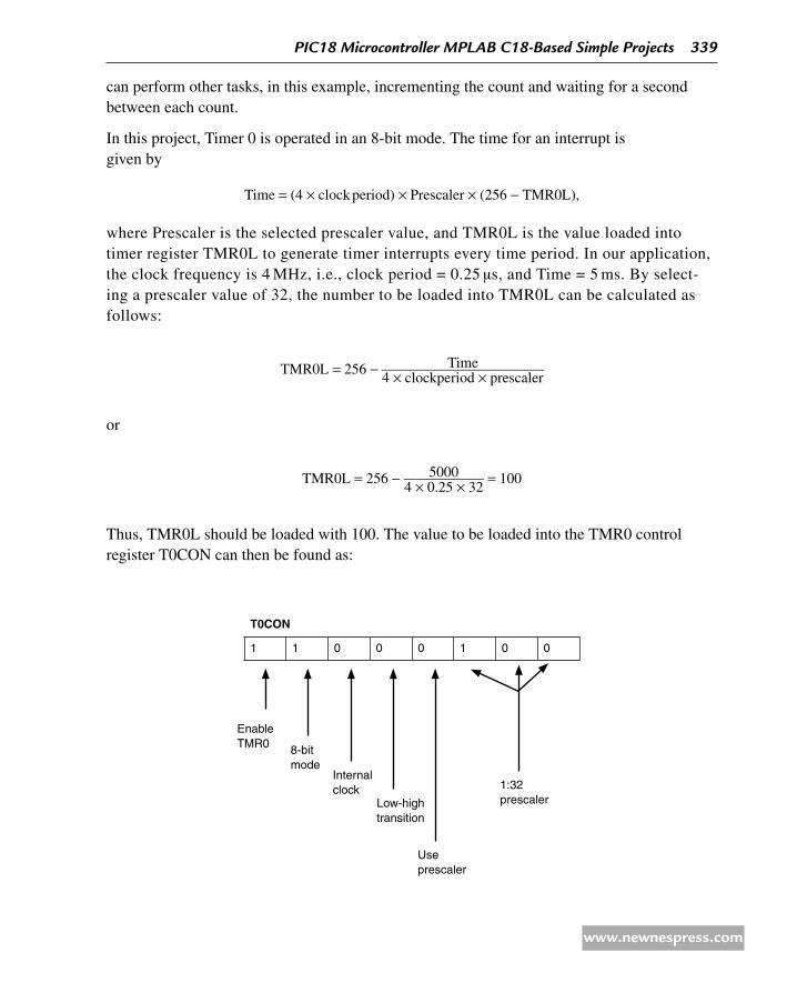
PIC18 Microcontroller MPLAB C18-Based simple Projects 339
www.newnespress.com
can perform other tasks, in this example, incrementing the count and waiting for a second between each count.
In this project, Timer 0 is operated in an 8-bit mode. The time for an interrupt is given by
Time = (4 × clock period) × Prescaler × (256 − TMR0L),
where Prescaler is the selected prescaler value, and TMR0L is the value loaded into timer register TMR0L to generate timer interrupts every time period. In our application, the clock frequency is 4 MHz, i.e., clock period = 0.25 μs, and Time = 5 ms. By select-ing a prescaler value of 32, the number to be loaded into TMR0L can be calculated as follows:
TMR0L = 256 − Time 4 × clockperiod × prescaler
or
TMR0L = 256 − 5000 4 × 0.25 × 32
= 100
Thus, TMR0L should be loaded with 100. The value to be loaded into the TMR0 control register T0CON can then be found as:
T0CON
1 1 0 0 0 1 0 0
Enable TMR0 8-bit
modeInternal clock
Low-high transition
Use prescaler
1:32 prescaler

340 Chapter 6
www.newnespress.com
Considering the don’t care entries (X) as 0, the hexadecimal value to be loaded into register INTCON is thus 0xA0.
When an interrupt occurs, the program automatically jumps to the ISR. Inside this routine, we have to reload register TMR0L, we also have to re-enable the TMR0 interrupts, and we have to clear the TMR0 interrupt flag bit. Setting the INTCON register to 0x20 re-enables the TMR0 interrupts and, at the same time, clears the TMR0 interrupt flag.
The operations to be performed in the main program can thus be summarized as follows:
Load TMR0L with 100 •
Set T0CON to 0xC4 •
Set INTCON to 0xA0 •
Increment the counter with 1-s delays •
The operations to be performed in the interrupt service routine can thus be summarized as follows:
Reload TMR0L to 100 •
Refresh displays •
Set INTCON to 0x20 (re-enable TMR0 interrupts and clear the timer interrupt flag) •
Thus, the T0CON register should be loaded with hexadecimal 0xC4. The next register to be configured is the interrupt control register INTCON, where we will disable priority-based interrupts and enable the global interrupts and TMR0 interrupts:
Clear TMR0IF
Enable global interrupts
Enable TMR0 int.
Disable INT0 int. Disable
RB change int.
INTCON
1 x 1 0 0 0 x x

PIC18 Microcontroller MPLAB C18-Based simple Projects 341
www.newnespress.com
682 Project Hardware
The circuit diagram of this project is same as in Figure 6.36, where a dual seven-segment display is connected to PORTB and PORTC of a PIC18F452 microcontroller.
683 Project PDL
The PDL of the project is shown in Figure 6.39. The program is in two sections: the main program and the ISR. Inside the main program, TMR0 is configured to generate interrupts every 5 ms. In addition, the counter is incremented with 1-s delay. Inside the ISR, the timer interrupt is re-enabled, and the display digits are refreshed alternately at every 5 ms.
684 Project Program
Before looking at the program code, it is worthwhile to describe how the interrupts are handled in the MPLAB C18 programs. The C18 compiler does not automatically start the ISR at the high or low interrupt vectors in program memory. The C18 compiler uses several pragmas, first to locate the start of the ISR at the reset vector and then to distinguish the ISR from a standard user function.
Figure 6.39: PdL of the Project
MAIN PROGRAM:
START Configure PORT B as outputs Configure PORT C as outputs Clear variable Cnt to 0 Configure TMR0 to generate interrupts every 5ms DO FOREVER Increment Cnt between 0 and 99 Delay 1 second ENDO END
INTERRUPT SERVICE ROUTINE: START Re-configure TMR0 IF Digit 1 updated THEN Update digit 2 ELSE Update digit 1 END END
342 Chapter 6
www.newnespress.com
The interrupt vector is specified in the program using the #pragma code statement. The high-priority vector is at address 0x08, and the low-priority vector is at address 0x18. To set the high-priority vector, the following statement is used:
#pragma code high_vector = 0x08
where the name high_vector is not a reserved name and any other name can be chosen by the programmer.
The above statement specifies that the code section that follows the statement starts at memory location 0x08. After the above statement, we have to write the following single line of assembly code to force a jump to the ISR:
_asm GOTO timer_ISR _endasm
where timer_ISR is the name of the ISR function. To return to the normal program code, we have to use the statement
#pragma code
Now, we have to use the following pragma statement to specify a high-priority ISR function:
#pragma interrupt timer_ISR
where interrupt is a reserved name, and timer_ISR is the name of the ISR function declared by the user. This function must follow the above statement.
If it is required to use a low-priority interrupt, then the above pragma statements should be changed to (assuming the name of the ISR function is timer_ISR)
#pragma code low_vector = 0x18
and
#pragma interruptlow timer_ISR
The program (called SEVEN4.C) is given in Figure 6.40. In this program function, prototypes are used at the beginning of the program to declare the functions called by the main program. At the beginning of the main program, PORTB and PORTC are configured as outputs. Then, register T0CON is loaded with 0xC4 to enable the TMR0 and set the prescaler to 32. TMR0L register is loaded with 100 so that an interrupt can be generated after 5 ms. The program then enters an endless loop, where the value of Cnt is incremented every second using a delay function.
Inside the ISR register, TMR0L is reloaded, TMR0 interrupts are re-enabled, and the timer interrupt flag is cleared so that further timer interrupts can be generated. The display digits are then updated alternately based on the value of variable Cnt. A variable called Flag is used to determine which digit to update. The function Display is called as in Project 6 to find the bit pattern to be sent to PORTC.

PIC18 Microcontroller MPLAB C18-Based simple Projects 343
www.newnespress.com
Figure 6.40: Program of the Project
/***********************************************************************************************************************************************Dual 7-SEGMENT DISPLAY COUNTER
==============================
In this project, two common cathode 7-segment LED displays are connected to PORT C of a PIC18F452 microcontroller and the microcontroller is operated from a 4-MHz resonator. Digit 1 (left digit) enable pin is connected to port pin RB0 and digit 2 (right digit) enable pin is connected to port pin RB1 of the microcontroller. The program counts up from 0 to 99 with a one-second delay between each count.
The display is updated in a timer interrupt service routine every 5 ms.
Author: Dogan IbrahimDate: June 2009File: SEVEN4.C***********************************************************************************************************************************************/#include <p18f452.h>#include <delays.h>#pragma config WDT = OFF, OSC = XT
#define DIGIT1 PORTBbits.RB0#define DIGIT2 PORTBbits.RB1
unsigned char Cnt = 0;unsigned char Flag = 0;
void One_Second_Delay(void);unsigned char Display(unsigned char);void timer_ISR(void);
//// Define the high interrupt vector to be at 0x08//#pragma code high_vector=0x08 //Following code at address 0x08void interrupt(void) _asm GOTO timer_ISR _endasm // Jump to ISR#pragma code // Return to default code section
//// timer_ISR is an interrupt service routine (jumps here every 5ms)//#pragma interrupt timer_ISRvoid timer_ISR( ) unsigned char Msd, Lsd; TMR0L = 100; // Re-load TMR0 INTCON = 0x20; // Set T0IE and clear T0IF Flag = ~ Flag; // Toggle Flag if(Flag == 0) // Do digit 1 DIGIT2 = 0; Msd = Cnt / 10; // MSD digit PORTC = Display(Msd); // Send to PORT C DIGIT1 = 1; // Enable digit 1 else // Do digit 2 DIGIT1 = 0; // Disable digit 1 Lsd = Cnt % 10; // LSD digit

344 Chapter 6
www.newnespress.com
Figure 6.40: Cont’d
PORTC = Display(Lsd); // Send to PORT C DIGIT2 = 1; // Enable digit 2
//// This function generates 1 second delay//void One_Second_Delay( ) Delay10KTCYx(100);
//// This function finds the bit pattern to be sent to the port to display a number// on the 7-segment LED. The number is passed in the argument list of the function.//unsigned char Display(unsigned char no) unsigned char Pattern; unsigned char SEGMENT[ ] = 0x3F,0x06,0x5B,0x4F,0x66,0x6D,0x7D,0x07, 0x7F,0x6F;
Pattern = SEGMENT[no]; // Pattern to return return (Pattern);
//// Start of MAIN Program. configure PORT B and PORT C as outputs. In addition,// configure TMR0 to interrupt at every 5ms//void main(void) TRISC = 0; // PORT C are outputs TRISB = 0; // RB0, RB1 are outputs
DIGIT1 = 0; // Disable digit 1 DIGIT2 = 0; // Disable digit 2//// Configure TMR0 timer interrupt// T0CON = 0xC4; // Prescaler = 32 TMR0L = 100; // Load TMR0L with 100 INTCON = 0xA0; // Enable TMR0 interrupt One_Second_Delay( );
for(;;) // Endless loop Cnt++; // Increment Cnt if(Cnt == 100) Cnt = 0; // Count between 0 and 99 One_Second_Delay( ); // Wait 1 second
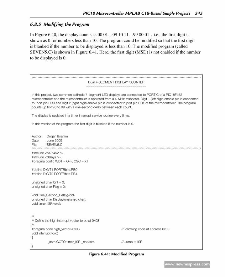
PIC18 Microcontroller MPLAB C18-Based simple Projects 345
www.newnespress.com
/***********************************************************************************************************************************************Dual 7-SEGMENT DISPLAY COUNTER
==============================
In this project, two common cathode 7-segment LED displays are connected to PORT C of a PIC18F452 microcontroller and the microcontroller is operated from a 4-MHz resonator. Digit 1 (left digit) enable pin is connected to port pin RB0 and digit 2 (right digit) enable pin is connected to port pin RB1 of the microcontroller. The program counts up from 0 to 99 with a one-second delay between each count.
The display is updated in a timer interrupt service routine every 5 ms.
In this version of the program the first digit is blanked if the number is 0.
Author: Dogan IbrahimDate: June 2009File: SEVEN5.C***********************************************************************************************************************************************/#include <p18f452.h>#include <delays.h>#pragma config WDT = OFF, OSC = XT
#define DIGIT1 PORTBbits.RB0#define DIGIT2 PORTBbits.RB1
unsigned char Cnt = 0;unsigned char Flag = 0;
void One_Second_Delay(void);unsigned char Display(unsigned char);void timer_ISR(void);
//// Define the high interrupt vector to be at 0x08//#pragma code high_vector=0x08 //Following code at address 0x08void interrupt(void) _asm GOTO timer_ISR _endasm // Jump to ISR
Figure 6.41: Modified Program
685 Modifying the Program
In Figure 6.40, the display counts as 00 01…09 10 11…99 00 01…i.e., the first digit is shown as 0 for numbers less than 10. The program could be modified so that the first digit is blanked if the number to be displayed is less than 10. The modified program (called SEVEN5.C) is shown in Figure 6.41. Here, the first digit (MSD) is not enabled if the number to be displayed is 0.
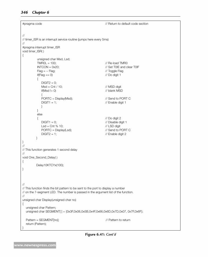
346 Chapter 6
www.newnespress.com
#pragma code // Return to default code section
//// timer_ISR is an interrupt service routine (jumps here every 5ms)//#pragma interrupt timer_ISRvoid timer_ISR( ) unsigned char Msd, Lsd; TMR0L = 100; // Re-load TMR0 INTCON = 0x20; // Set T0IE and clear T0IF Flag = ~ Flag; // Toggle Flag if(Flag == 0) // Do digit 1 DIGIT2 = 0; Msd = Cnt / 10; // MSD digit if(Msd != 0) // blank MSD PORTC = Display(Msd); // Send to PORT C DIGIT1 = 1; // Enable digit 1 else // Do digit 2 DIGIT1 = 0; // Disable digit 1 Lsd = Cnt % 10; // LSD digit PORTC = Display(Lsd); // Send to PORT C DIGIT2 = 1; // Enable digit 2 //// This function generates 1 second delay//void One_Second_Delay( ) Delay10KTCYx(100);
//// This function finds the bit pattern to be sent to the port to display a number// on the 7-segment LED. The number is passed in the argument list of the function.//unsigned char Display(unsigned char no) unsigned char Pattern; unsigned char SEGMENT[ ] = 0x3F,0x06,0x5B,0x4F,0x66,0x6D,0x7D,0x07, 0x7F,0x6F;
Pattern = SEGMENT[no]; // Pattern to return return (Pattern);
Figure 6.41: Cont’d

PIC18 Microcontroller MPLAB C18-Based simple Projects 347
www.newnespress.com
6.9 Project 8 – Four-digit Multiplexed Seven-Segment Led Counter With timer interrupt
691 Project Description
This project is similar to Project 7, but a 4-digit display is used instead of a 2-digit display. Thus, any integer in the range from 0 to 9999 can be displayed. As in Project 7, the display is updated in the ISR; consequently, the processor can perform other tasks while the display is updated in the background. In this project, the value of a counter is displayed as it counts up every second. The operation of this project is very similar to that of Project 7; therefore, the project is not described again here in detail.
692 Project Hardware
The circuit diagram of this project is shown in Figure 6.42, where four 7-segment displays are connected to PORTB and PORTC of a PIC18F452 microcontroller. The segments are con-nected in parallel to PORTC, and they are enabled from PORTB.
//// Start of MAIN Program. configure PORT B and PORT C as outputs. In addition,// configure TMR0 to interrupt at every 5ms//void main(void) TRISC = 0; // PORT C are outputs TRISB = 0; // RB0, RB1 are outputs
DIGIT1 = 0; // Disable digit 1 DIGIT2 = 0; // Disable digit 2//// Configure TMR0 timer interrupt// T0CON = 0xC4; // Prescaler = 32 TMR0L = 100; // Load TMR0L with 100 INTCON = 0xA0; // Enable TMR0 interrupt One_Second_Delay( );
for(;;) // Endless loop Cnt++; // Increment Cnt if(Cnt == 100) Cnt = 0; // Count between 0 and 99 One_Second_Delay( ); // Wait 1 second
Figure 6.41: Cont’d

348 Chapter 6
www.newnespress.com
693 Project PDL
The PDL of the project is shown in Figure 6.43. The program is in two sections: the main program and the ISR. Inside the main program, TMR0 is configured to generate interrupts every 5 ms. In addition, the counter is incremented with a 1-s delay. Inside the ISR, the timer interrupt is re-enabled, and the display digits are refreshed alternately every 5 ms.
694 Project Program
The program (called SEVEN6.C) is given in Figure 6.44. In this program, function prototypes are used at the beginning of the program to declare the functions called by the main program. At the beginning of the main program, PORTB and PORTC are configured as outputs. Then, register T0CON is loaded with 0xC4 to enable the TMR0 and set the prescaler to 32. The TMR0L register is loaded with 100 so that an interrupt can be generated after 5 ms. The program then enters an endless loop, where the value of Cnt is incremented every second using a delay function.
Figure 6.42: Circuit diagram of the Project
RC0
RC1
RC2
RC3
RC4
RC5
RC6
RB0RB1RB2RB3
OSC2OSC1
Vss
MCLR
Vdd
11 32
15 V
10 K1
12
31 33
25
1218
1718
1231516
a16
abcdefg
11151038261517
1812
7
1611151038261517
7
DC56-11EWA DC56-11EWA
bcdefg
E1 E2 E1 E2
24
23
18
17
16
15 290
290
290
290
290
290
290
34 14
BC1081 K
13
BC1081 K
14
BC1081 K
13
BC1081 K
3536
13
4 MHz resonator
14
PIC18F452

PIC18 Microcontroller MPLAB C18-Based simple Projects 349
www.newnespress.com
MAIN PROGRAM:
START Configure PORT B as outputs Configure PORT C as outputs Clear variable Cnt to 0 Configure TMR0 to generate interrupts every 5ms DO FOREVER Increment Cnt between 0 and 99 Delay 1 second ENDO END
INTERRUPT SERVICE ROUTINE: START Re-configure TMR0 IF Digit 1 updated THEN Update digit 2 ELSE IF Digit 2 is updated THEN Update digit 3 ELSE IF Digit 3 is updated THEN Update digit 4 ELSE IF Digit 4 is updated THEN Update digit 1 END END
Figure 6.43: PdL of the Project
Figure 6.44: Program of the Project
/**********************************************************************************************************************************************Four 7-SEGMENT DISPLAY COUNTER
==============================
In this project, four common cathode 7-segment LED displays are connected to PORT C of a PIC18F452 microcontroller and the microcontroller is operated from a 4-MHz resonator. Digit 1 (left digit) enable pin is connected to port pin RB0, digit 2 enable pin is connected to port pin RB1. Digit 3 enable pin is connected to port pin RB2 and digit 4 (right digit) enable pin is connected to port pin RB3.
The program counts up from 0 to 9999 with a one-second delay between each count.
The display is updated in a timer interrupt service routine every 5 ms.
Author: Dogan IbrahimDate: June 2009File: SEVEN6.C***********************************************************************************************************************************************/#include <p18f452.h>#include <delays.h>#pragma config WDT = OFF, OSC = XT#define DIGIT1 PORTBbits.RB0
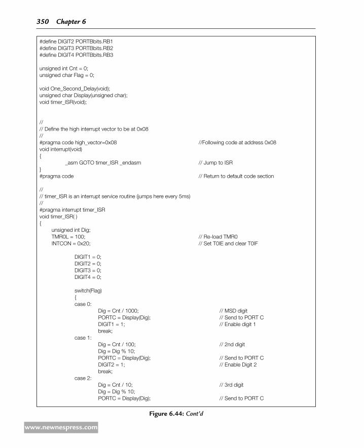
350 Chapter 6
www.newnespress.com
Figure 6.44: Cont’d
#define DIGIT2 PORTBbits.RB1#define DIGIT3 PORTBbits.RB2#define DIGIT4 PORTBbits.RB3
unsigned int Cnt = 0;unsigned char Flag = 0;
void One_Second_Delay(void);unsigned char Display(unsigned char);void timer_ISR(void);
//// Define the high interrupt vector to be at 0x08//#pragma code high_vector=0x08 //Following code at address 0x08void interrupt(void) _asm GOTO timer_ISR _endasm // Jump to ISR#pragma code // Return to default code section
//// timer_ISR is an interrupt service routine (jumps here every 5ms)//#pragma interrupt timer_ISRvoid timer_ISR( ) unsigned int Dig; TMR0L = 100; // Re-load TMR0 INTCON = 0x20; // Set T0IE and clear T0IF DIGIT1 = 0; DIGIT2 = 0; DIGIT3 = 0; DIGIT4 = 0;
switch(Flag) case 0: Dig = Cnt / 1000; // MSD digit PORTC = Display(Dig); // Send to PORT C DIGIT1 = 1; // Enable digit 1 break; case 1: Dig = Cnt / 100; // 2nd digit Dig = Dig % 10; PORTC = Display(Dig); // Send to PORT C DIGIT2 = 1; // Enable Digit 2 break; case 2: Dig = Cnt / 10; // 3rd digit Dig = Dig % 10; PORTC = Display(Dig); // Send to PORT C
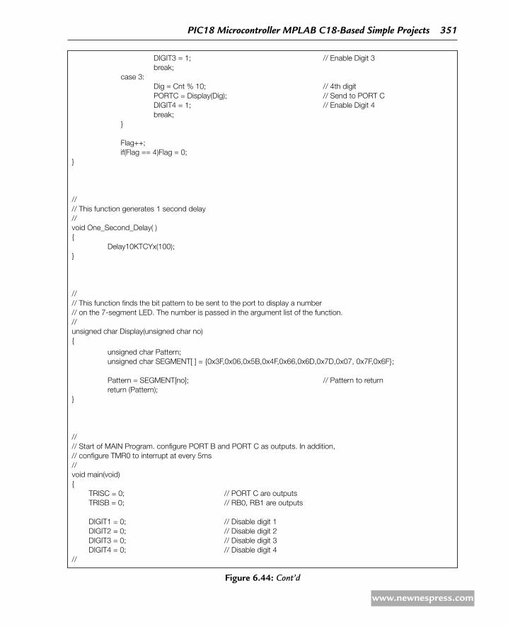
PIC18 Microcontroller MPLAB C18-Based simple Projects 351
www.newnespress.com
Figure 6.44: Cont’d
DIGIT3 = 1; // Enable Digit 3 break; case 3: Dig = Cnt % 10; // 4th digit PORTC = Display(Dig); // Send to PORT C DIGIT4 = 1; // Enable Digit 4 break;
Flag++; if(Flag == 4)Flag = 0;
//// This function generates 1 second delay//void One_Second_Delay( ) Delay10KTCYx(100);
//// This function finds the bit pattern to be sent to the port to display a number// on the 7-segment LED. The number is passed in the argument list of the function.//unsigned char Display(unsigned char no)
unsigned char Pattern; unsigned char SEGMENT[ ] = 0x3F,0x06,0x5B,0x4F,0x66,0x6D,0x7D,0x07, 0x7F,0x6F;
Pattern = SEGMENT[no]; // Pattern to return return (Pattern);
//// Start of MAIN Program. configure PORT B and PORT C as outputs. In addition,// configure TMR0 to interrupt at every 5ms//void main(void) TRISC = 0; // PORT C are outputs TRISB = 0; // RB0, RB1 are outputs
DIGIT1 = 0; // Disable digit 1 DIGIT2 = 0; // Disable digit 2 DIGIT3 = 0; // Disable digit 3 DIGIT4 = 0; // Disable digit 4//

352 Chapter 6
www.newnespress.com
Inside the ISR register, TMR0L is reloaded, TMR0 interrupts are re-enabled, and the timer interrupt flag is cleared so that further timer interrupts can be generated. The display digits are then updated based on the value of variable Cnt. A variable called Flag is used to determine which digit to update. Flag varies between 0 and 3, and the display digits are updated in a switch statement as follows:
Flag digit Updated
0 1 (MSD)
1 2
2 3
3 4 (LSD)
Function Display is called as in Project 7 to find the bit pattern to be sent to PORTC.
695 Modifying the Program
In Figure 6.44, the display counts as 0000 0001…0009 0010 0011…9999 0000 0001…i.e., the leading digits are shown even when they are zero. The program could be modified so that the leading digits are blanked if the corresponding digits are zero. The modified program (called SEVEN7.C) is shown in Figure 6.45. Note that the first digit is enabled if the number is greater than or equal to 1000, the second digit is enabled if the number is greater than or equal to 100, and the third digit is enabled if the number is greater than or equal to 10.
696 Using MPLAB C18 Compiler Timer Library Routines
In the previous examples, the timer TMR0 was configured by writing into the timer regis-ters. MPLAB C18 compiler provides timer library routines that simplify the configuration of timers. The program given in Figure 6.45 has been modified to use these timer library
// Configure TMR0 timer interrupt// T0CON = 0xC4; // Prescaler = 32 TMR0L = 100; // Load TMR0L with 100 INTCON = 0xA0; // Enable TMR0 interrupt One_Second_Delay( );
for(;;) // Endless loop Cnt++; // Increment Cnt if(Cnt == 10000) Cnt = 0; // Count between 0 and 9999 One_Second_Delay( ); // Wait 1 second
Figure 6.44: Cont’d

PIC18 Microcontroller MPLAB C18-Based simple Projects 353
www.newnespress.com
/**********************************************************************************************************************************************Four 7-SEGMENT DISPLAY COUNTER
==============================
In this project, four common cathode 7-segment LED displays are connected to PORT C of a PIC18F452 microcontroller and the microcontroller is operated from a 4-MHz resonator. Digit 1 (left digit) enable pin is connected to port pin RB0, digit 2 enable pin is connected to port pin RB1. Digit 3 enable pin is connected to port pin RB2 and digit 4 (right digit) enable pin is connected to port pin RB3.
The program counts up from 0 to 9999 with a 1-second delay between each count.
The display is updated in a timer interrupt service routine at every 5 ms.In this version of the program, leading zeroes are blanked.
Author: Dogan IbrahimDate: June 2009File: SEVEN7.C***********************************************************************************************************************************************/#include <p18f452.h>#include <delays.h>#pragma config WDT = OFF, OSC = XT
#define DIGIT1 PORTBbits.RB0#define DIGIT2 PORTBbits.RB1#define DIGIT3 PORTBbits.RB2#define DIGIT4 PORTBbits.RB3
unsigned int Cnt = 0;unsigned char Flag = 0;
void One_Second_Delay(void);unsigned char Display(unsigned char);void timer_ISR(void);
//// Define the high interrupt vector to be at 0x08//#pragma code high_vector=0x08 //Following code at address 0x08void interrupt(void) _asm GOTO timer_ISR _endasm // Jump to ISR#pragma code // Return to default code section
//// timer_ISR is an interrupt service routine (jumps here every 5ms)//#pragma interrupt timer_ISRvoid timer_ISR( ) unsigned int Dig; TMR0L = 100; // Re-load TMR0 INTCON = 0x20; // Set T0IE and clear T0IF
Figure 6.45: Modified Program

354 Chapter 6
www.newnespress.com
DIGIT1 = 0; DIGIT2 = 0; DIGIT3 = 0; DIGIT4 = 0;
switch(Flag)
case 0: if(Cnt >= 1000) Dig = Cnt / 1000; // MSD digit PORTC = Display(Dig); // Send to PORT C DIGIT1 = 1; // Enable digit 1 break;
case 1: if(Cnt >= 100) Dig = Cnt / 100; // 2nd digit Dig = Dig % 10; PORTC = Display(Dig); // Send to PORT C DIGIT2 = 1; // Enable Digit 2 break;
case 2: if(Cnt >= 10) Dig = Cnt / 10; // 3rd digit Dig = Dig % 10; PORTC = Display(Dig); // Send to PORT C DIGIT3 = 1; // Enable Digit 3 break;
case 3: Dig = Cnt % 10; // 4th digit PORTC = Display(Dig); // Send to PORT C DIGIT4 = 1; // Enable Digit 4 break; Flag++; if(Flag == 4)Flag = 0;
//// This function generates 1 second delay//void One_Second_Delay( ) Delay10KTCYx(100);
Figure 6.45: Cont’d

PIC18 Microcontroller MPLAB C18-Based simple Projects 355
www.newnespress.com
routines. The modified program (called SEVEN8.C) is given in Figure 6.46. As can be seen in this program, the header file <timers.h> should be declared as the beginning of the program. In the main program, the timer TMR0 is configured by calling the library function OpenTimer0
OpenTimer0(TIMER_INT_ON & T0_8BIT & T0_SOURCE_INT & T0_PS_1_32);
//// This function finds the bit pattern to be sent to the port to display a number// on the 7-segment LED. The number is passed in the argument list of the function.//unsigned char Display(unsigned char no) unsigned char Pattern; unsigned char SEGMENT[ ] = 0x3F,0x06,0x5B,0x4F,0x66,0x6D,0x7D,0x07,0x7F,0x6F;
Pattern = SEGMENT[no]; // Pattern to return return (Pattern);
//// Start of MAIN Program. configure PORT B and PORT C as outputs. In addition,// configure TMR0 to interrupt at every 5ms//void main(void) TRISC = 0; // PORT C are outputs TRISB = 0; // RB0, RB1 are outputs
DIGIT1 = 0; // Disable digit 1 DIGIT2 = 0; // Disable digit 2 DIGIT3 = 0; // Disable digit 3 DIGIT4 = 0; // Disable digit 4//// Configure TMR0 timer interrupt// T0CON = 0xC4; // Prescaler = 32 TMR0L = 100; // Load TMR0L with 100 INTCON = 0xA0; // Enable TMR0 interrupt One_Second_Delay( );
for(;;) // Endless loop Cnt++; // Increment Cnt if(Cnt == 10000) Cnt = 0; // Count between 0 and 9999 One_Second_Delay( ); // Wait 1 second
Figure 6.45: Cont’d
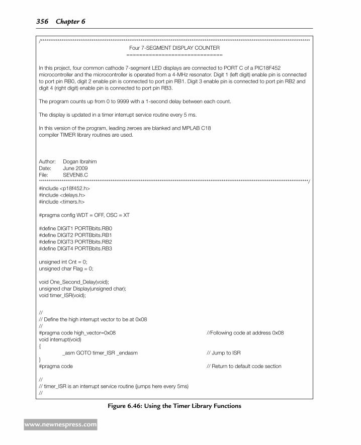
356 Chapter 6
www.newnespress.com
/***********************************************************************************************************************************************Four 7-SEGMENT DISPLAY COUNTER
==============================
In this project, four common cathode 7-segment LED displays are connected to PORT C of a PIC18F452 microcontroller and the microcontroller is operated from a 4-MHz resonator. Digit 1 (left digit) enable pin is connected to port pin RB0, digit 2 enable pin is connected to port pin RB1. Digit 3 enable pin is connected to port pin RB2 and digit 4 (right digit) enable pin is connected to port pin RB3.
The program counts up from 0 to 9999 with a 1-second delay between each count.
The display is updated in a timer interrupt service routine every 5 ms.
In this version of the program, leading zeroes are blanked and MPLAB C18compiler TIMER library routines are used.
Author: Dogan IbrahimDate: June 2009File: SEVEN8.C***********************************************************************************************************************************************/#include <p18f452.h>#include <delays.h>#include <timers.h>
#pragma config WDT = OFF, OSC = XT
#define DIGIT1 PORTBbits.RB0#define DIGIT2 PORTBbits.RB1#define DIGIT3 PORTBbits.RB2#define DIGIT4 PORTBbits.RB3
unsigned int Cnt = 0;unsigned char Flag = 0;
void One_Second_Delay(void);unsigned char Display(unsigned char);void timer_ISR(void);
//// Define the high interrupt vector to be at 0x08//#pragma code high_vector=0x08 //Following code at address 0x08void interrupt(void) _asm GOTO timer_ISR _endasm // Jump to ISR#pragma code // Return to default code section
//// timer_ISR is an interrupt service routine (jumps here every 5ms)//
Figure 6.46: Using the timer Library Functions

PIC18 Microcontroller MPLAB C18-Based simple Projects 357
www.newnespress.com
#pragma interrupt timer_ISRvoid timer_ISR( ) unsigned int Dig; WriteTimer0(100); // Re-load TMR0 INTCON = 0x20; // Set T0IE and clear T0IF
DIGIT1 = 0; DIGIT2 = 0; DIGIT3 = 0; DIGIT4 = 0;
switch(Flag) case 0: if(Cnt >= 1000) Dig = Cnt / 1000; // MSD digit PORTC = Display(Dig); // Send to PORT C DIGIT1 = 1; // Enable Digit 1 break; case 1: if(Cnt >= 100) Dig = Cnt / 100; // 2nd digit Dig = Dig % 10; PORTC = Display(Dig); // Send to PORT C DIGIT2 = 1; // Enable Digit 2 break; case 2: if(Cnt >= 10) Dig = Cnt / 10; // 3rd digit Dig = Dig % 10; PORTC = Display(Dig); // Send to PORT C DIGIT3 = 1; // Enable Digit 3 break; case 3: Dig = Cnt % 10; // 4th digit PORTC = Display(Dig); // Send to PORT C DIGIT4 = 1; // Enable Digit 4 break; Flag++; if(Flag == 4)Flag = 0;
//
Figure 6.46: Cont’d
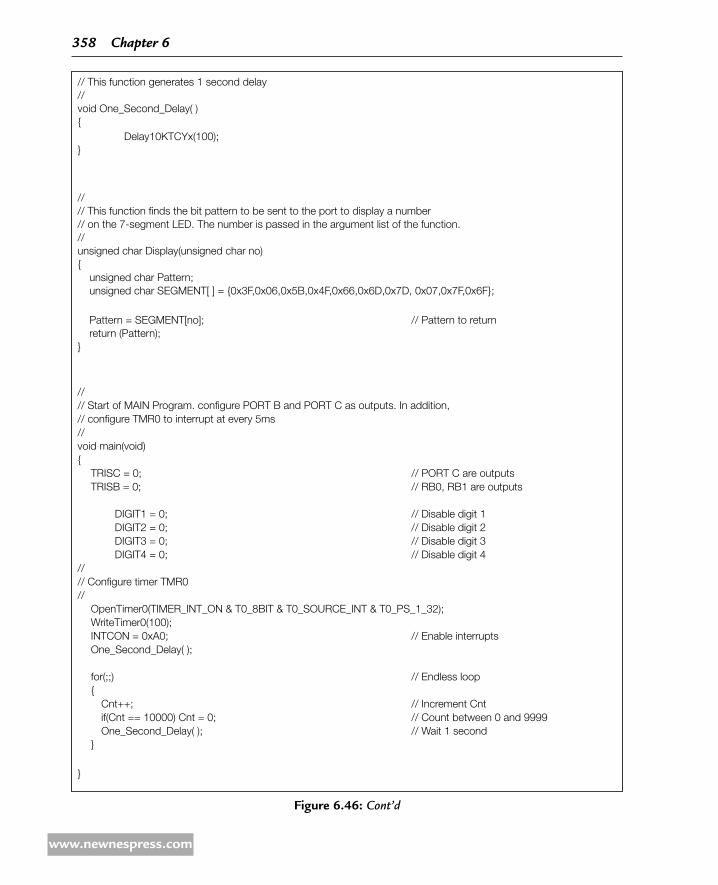
358 Chapter 6
www.newnespress.com
// This function generates 1 second delay//void One_Second_Delay( ) Delay10KTCYx(100);
//// This function finds the bit pattern to be sent to the port to display a number// on the 7-segment LED. The number is passed in the argument list of the function.//unsigned char Display(unsigned char no) unsigned char Pattern; unsigned char SEGMENT[ ] = 0x3F,0x06,0x5B,0x4F,0x66,0x6D,0x7D, 0x07,0x7F,0x6F;
Pattern = SEGMENT[no]; // Pattern to return return (Pattern);
//// Start of MAIN Program. configure PORT B and PORT C as outputs. In addition,// configure TMR0 to interrupt at every 5ms//void main(void) TRISC = 0; // PORT C are outputs TRISB = 0; // RB0, RB1 are outputs
DIGIT1 = 0; // Disable digit 1 DIGIT2 = 0; // Disable digit 2 DIGIT3 = 0; // Disable digit 3 DIGIT4 = 0; // Disable digit 4//// Configure timer TMR0// OpenTimer0(TIMER_INT_ON & T0_8BIT & T0_SOURCE_INT & T0_PS_1_32); WriteTimer0(100); INTCON = 0xA0; // Enable interrupts One_Second_Delay( );
for(;;) // Endless loop Cnt++; // Increment Cnt if(Cnt == 10000) Cnt = 0; // Count between 0 and 9999 One_Second_Delay( ); // Wait 1 second
Figure 6.46: Cont’d
PIC18 Microcontroller MPLAB C18-Based simple Projects 359
www.newnespress.com
This function has been called with the following arguments:
Enable timer interrupts.
Use timer in 8-bit mode.
Use internal clock source for the timer.
Use 1:32 prescaler value.
The timer is loaded by calling function WriteTimer0 and specifying the timer value as the argument.
WriteTimer0(100);
6.10 Summary
In this chapter, working examples of microcontroller C programs developed using the MPLAB C18 compiler are given. These examples should be very useful to readers who are new to programming the PIC microcontrollers using the C language.
6.11 exercises
It is required to connect eight LEDs to PORTB of a PIC18F452-type microcontroller. 1. Draw the circuit diagram of the project assuming that the microcontroller is to be operated from a 4-MHz crystal. Write a C program to turn ON the odd-numbered LEDs (i.e., LEDs connected to RB1, RB3, RB5, and RB7).
Eight LEDs are connected to a microcontroller as in Exercise 1. Write a C program to 2. turn the LEDs ON and OFF every minute. Use C18 delay routines in your program.
Eight LEDs are connected to a microcontroller as in Exercise 1. Write a C program using 3. TMR0 interrupts to turn the LEDs ON and OFF every 500 ms.
It is required to test a two-input NAND gate using a microcontroller. Assume that the 4. inputs of the NAND gate are connected to ports RB0 and RB1, and the output is connected to port RB2. In addition, an LED is connected to port RB7. Draw the circuit diagram of the project and also write a C program to test the gate. If the gate is faulty, turn ON the LED, otherwise the LED should remain OFF.
Repeat Exercise 4, but this time, write a C program to test a NOR gate. 5.
Write a C program to use TMR0 in a 16-bit mode and generate timer interrupts at 1-s 6. intervals. Assume that an LED is connected to port RB7 of the microcontroller and turn this LED ON and OFF every 5 s.

This page intentionally left blank

© 2010 Elsevier Ltd. All rights reserved.D.O.I.: 10.1016/B978-1-85617-719-1.00011-7
ChaPter 7
serial Peripheral Interface Bus Operation
As described in Chapter 3, the secure digital (SD) card will be used in serial peripheral interface (SPI) bus mode. Before looking at the MPLAB C18 SD card functions and sub-programs, it is worthwhile to see how the PIC18 microcontrollers can be configured and used in SPI mode. With a good understanding of the operation of the SPI bus, the SD card functions and subprograms can easily be modified if required.
In this chapter, the configuration and operation of the PIC18 microcontrollers in SPI mode will be described and then an MPLAB C18-based example will be given to show how the microcontrollers can be programmed and used for SPI operation using a real external device.
7.1 the Master Synchronous Serial Port Module
The master synchronous serial port (MSSP) module is a serial interface module on the PIC18 series of microcontrollers used for communicating with other serial devices, such as EEPROMs, display drivers, A/D converters, D/A converters, and so on.
The MSSP module can operate in one of two modes:
SPI •
Inter-integrated circuit (I • 2C)
Both SPI and I2C are serial bus protocol standards. The SPI protocol was initially developed and proposed by Motorola for use in microprocessor- and microcontroller-based interface appli-cations. In a system that uses the SPI bus, one device acts as the master and other devices act as slaves. The master initiates a communication and also provides clock pulses to the slave devices.
The I2C is a two-wire bus and was initially developed by Philips for use in low-speed microprocessor-based communication applications.
In this chapter, we shall be looking at the operation of the MSSP module in SPI mode.
7.2 MSSP in SPi Mode
The SPI mode allows 8 bits of data to be transmitted synchronously and received simultaneously. In master mode, the device uses three signals, and in slave mode, a fourth signal is used. In this chapter, we shall be looking at how to use the MSSP module in master
361
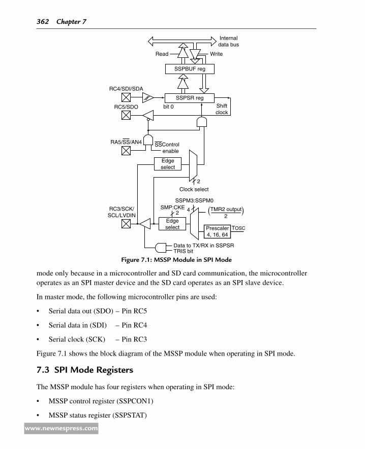
mode only because in a microcontroller and SD card communication, the microcontroller operates as an SPI master device and the SD card operates as an SPI slave device.
In master mode, the following microcontroller pins are used:
Serial data out (SDO) – Pin RC5 •
Serial data in (SDI) – Pin RC4 •
Serial clock (SCK) – Pin RC3 •
Figure 7.1 shows the block diagram of the MSSP module when operating in SPI mode.
7.3 SPi Mode registers
The MSSP module has four registers when operating in SPI mode:
MSSP control register (SSPCON1) •
MSSP status register (SSPSTAT) •
Figure 7.1: MSSP Module in SPi Mode
Read Write
SSPBUF reg
RC4/SDI/SDA
RA5/SS/AN4
RC3/SCK/SCL/LVDIN
Edgeselect
Data to TX/RX in SSPSR
Prescaler4, 16, 64
TOSC
TRIS bit
SSControlenable
Edgeselect
2
Clock select
SSPM3:SSPM0
TMR2 output2
SMP:CKE2 4
RC5/SDO
SSPSR reg
Shiftclock
bit 0
Internaldata bus
362 Chapter 7
www.newnespress.com

Serial receive/transmit buffer register (SSPBUF) •
MSSP shift register (not accessible by the programmer) •
731 ssPsTAT
SSPSTAT is the status register, with the lower 6 bits read only and the upper 2 bits read/write. Figure 7.2 shows the bit definitions of this register. Only bits 0, 6, and 7 are related to operation in SPI mode. Bit 7 (SMP) allows the user to select the input data sample time. When SMP = 0, input data is sampled at the middle of data output time, and when SMP = 1, the sampling is done at the end. Bit 6 (CKE) allows the user to select the transmit clock
Figure 7.2: SSPStat register Bit Configuration
R/W-0 R/W-0 R-0 R-0 R-0 R-0 R-0 R-0
SMP CKE D/A P S R/W UA BF
bit 7 bit 0
bit 7 SMP: Sample bitSPI Master mode:1 = Input data sampled at end of data output time0 = Input data sampled at middle of data output timeSPI Slave mode:SMP must be cleared when SPI is used in slave mode
bit 6 CKE: SPI clock edge selectWhen CKP = 0:1 = Data transmitted on the rising edge of SCK0 = Data transmitted on the falling edge of SCKWhen CKP = 1:1 = Data transmitted on the falling edge of SCK0 = Data transmitted on the rising edge of SCK
bit 5 D/A: Data address bitUsed in I2C mode only
bit 4 P: STOP bit Used in I2C mode only. This bit is cleared when the MSSP module is disabled, SSPEN is cleared.
bit 3 S: START bitUsed in I2C mode only
bit 2 R/W: Read write bit informationUsed in I2C mode only
bit 1 UA: Update addressUsed in I2C mode only
bit 0 BF: Buffer full status bit (receive mode only)1 = Recevie complete, SSPBUF is full0 = Receive not complete, SSPBUF is empty
Legend: R = Readable bit W = Writable bit U = Unimplemented bit, read as ‘0’-n = Value at POR ‘I’ = Bit is set ‘0’ = Bit is cleared × = Bit is unknown
serial Peripheral Interface Bus Operation 363
www.newnespress.com

edge. When CKE = 0, transmit occurs on transition from idle to active clock state, and when CKE = 1, transmit occurs on transition from active to idle clock state. Bit 0 (BF) is the buffer full status bit. When BF = 1, receive is complete (i.e., SSPBUF is full), and when BF = 0, receive is not complete (i.e., SSPBUF is empty).
732 ssPCON1
SSPCON1 is the control register (see Figure 7.3) used to enable the SPI mode and to set the clock polarity (CP) and the clock frequency. In addition, the transmit collision detection (bit 7) and the receive overflow detection (bit 6) are indicated by this register.
Figure 7.3: SSPCON1 register Bit Configuration
R/W-0 R/W-0 R-0 R-0 R-0 R-0 R-0 R-0
SMP CKE D/A P S R/W UA BF
bit 7 bit 0
bit 7 SMP: Sample bitSPI Master mode:1 = Input data sampled at end of data output time0 = Input data sampled at middle of data output timeSPI Slave mode:SMP must be cleared when SPI is used in slave mode
bit 6 CKE: SPI clock edge selectWhen CKP = 0:1 = Data transmitted on the rising edge of SCK0 = Data transmitted on the falling edge of SCKWhen CKP = 1:1 = Data transmitted on the falling edge of SCK0 = Data transmitted on the rising edge of SCK
bit 5 D/A: Data address bitUsed in I2C mode only
bit 4 P: STOP bit Used in I2C mode only. This bit is cleared when the MSSP module is disabled, SSPEN is cleared.
bit 3 S: START bitUsed in I2C mode only
bit 2 R/W: Read write bit informationUsed in I2C mode only
bit 1 UA: Update addressUsed in I2C mode only
bit 0 BF: Buffer full status bit (receive mode only)1 = Receive complete, SSPBUF is full0 = Receive not complete, SSPBUF is empty
Legend: R = Readable bit W = Writable bit U = Unimplemented bit, read as ‘0’-n = Value at POR ‘I’ = Bit is set ‘0’ = Bit is cleared × = Bit is unknown
364 Chapter 7
www.newnespress.com
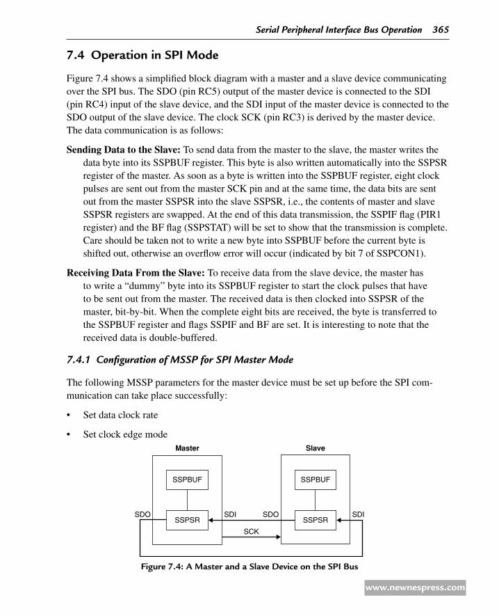
7.4 Operation in SPi Mode
Figure 7.4 shows a simplified block diagram with a master and a slave device communicating over the SPI bus. The SDO (pin RC5) output of the master device is connected to the SDI (pin RC4) input of the slave device, and the SDI input of the master device is connected to the SDO output of the slave device. The clock SCK (pin RC3) is derived by the master device. The data communication is as follows:
Sending Data to the Slave: To send data from the master to the slave, the master writes the data byte into its SSPBUF register. This byte is also written automatically into the SSPSR register of the master. As soon as a byte is written into the SSPBUF register, eight clock pulses are sent out from the master SCK pin and at the same time, the data bits are sent out from the master SSPSR into the slave SSPSR, i.e., the contents of master and slave SSPSR registers are swapped. At the end of this data transmission, the SSPIF flag (PIR1 register) and the BF flag (SSPSTAT) will be set to show that the transmission is complete. Care should be taken not to write a new byte into SSPBUF before the current byte is shifted out, otherwise an overflow error will occur (indicated by bit 7 of SSPCON1).
Receiving Data From the Slave: To receive data from the slave device, the master has to write a “dummy” byte into its SSPBUF register to start the clock pulses that have to be sent out from the master. The received data is then clocked into SSPSR of the master, bit-by-bit. When the complete eight bits are received, the byte is transferred to the SSPBUF register and flags SSPIF and BF are set. It is interesting to note that the received data is double-buffered.
741 Configuration of MssP for sPI Master Mode
The following MSSP parameters for the master device must be set up before the SPI com-munication can take place successfully:
Set data clock rate •
Set clock edge mode •
Figure 7.4: a Master and a Slave device on the SPi Bus
SSPBUF SSPBUF
SSPSR SSPSR
SCK
SDOSDI SDISDO
Master Slave
serial Peripheral Interface Bus Operation 365
www.newnespress.com

Clear bit 5 of TRISC (i.e., SDO • = RC5 is output)
Clear bit 3 of TRISC (i.e., SCK • = RC3 is output)
Enable the SPI mode •
Note that the SDI pin (pin RC4) direction is automatically controlled by the SPI module.
Data Clock Rate
The clock is derived by the master, and the clock rate is user programmable to one of the following values via the SSPCON1 register bits 0–3 (see Figure 7.3):
Fosc/4 •
Fosc/16 •
Fosc/64 •
Timer 2 output/2 •
Clock Edge Mode
The clock edge is user programmable via register SSPCON1 (bit 4), and the user can either set the clock edge as idle high or idle low. In the idle high mode, the clock is high when the device is not transmitting, and in the idle low mode, the clock is low when the device is not transmitting. Data can be transmitted either at the rising or at the falling edge of the clock. The CKE bit of SSPSTAT (bit 6) is used to select the clock edge.
Enabling the SPI Mode
Bit 5 of SSPCON1 must be set to enable the SPI mode. To reconfigure the SPI parameters, this bit must be cleared, SPI mode configured, and then the SSPEN bit set back to 1.
The example given below demonstrates how to set the SPI parameters.
example 7.1
It is required to operate the MSSP device of a PIC microcontroller in SPI mode. The data should be shifted on the rising edge of the clock, and the SCK signal must be idle low. The required data rate is at least 1 Mbps. Assume that the microcontroller clock rate is 16 MHz and the input data is to be sampled at the middle of data output time. What should be the settings of the MSSP registers?
solution
Register SSPCON1 should be set as follows:
Clear bits 6 and 7 of SSPCON1 (i.e., no collision detect and no overflow). •
366 Chapter 7
www.newnespress.com

Clear bits 4 to 0 to select idle low for the clock. •
Set bits 0 through 3 to 0000 or 0001 to select the clock rate to Fosc/4 (i.e., 16/4 • = 4 Mbps data rate) or Fosc/16 (i.e., 16/16 = 1 Mbps).
Set bit 5 to enable the SPI mode. •
Thus, register SSPCON1 should be set to the following bit pattern:
00 1 0 0000 i.e., 0 × 20
Register SSPSTAT should be set as follows:
Clear bit 7 to sample the input data at the middle of data output time. •
Clear bit 6 to 0 to transmit the data on the rising edge (low-to-high) of the SCK •clock.
Bits 5 through 0 are not used in the SPI mode. •
Thus, register SSPSTAT should be set to the following bit pattern:
0 0 0 00000 i.e., 0 × 00
7.5 SPi Bus MPLaB C18 Library Functions
MPLAB C18 compiler provides useful library functions for programming the MSSP module in SPI mode. These library functions are shown in Table 7.1 (see the Microchip document MPLAB C18 C Compiler Libraries for more details).
The header file spi.h must be included at the beginning of the C18 programs to use these functions. The available functions are briefly described below.
table 7.1: MPLaB C18 SPi Library Functions
Functions descriptions
CloseSPI Disable the SPI module
DataRdySPIDetermine whether a data byte is available on the
SPI bus
getcSPI Read a byte from the SPI bus
getsSPI Read a string from the SPI bus
OpenSPI Initialize the SPI module
putcSPI Write a byte to the SPI bus
putsSPI Write a string to the SPI bus
ReadSPI Read a byte from the SPI bus
WriteSPI Write a byte to the SPI bus
serial Peripheral Interface Bus Operation 367
www.newnespress.com
751 ClosesPI
Description: This function disables the SPI module.Example code: closeSPI();
752 DataRdysPI
Description: This function determines whether the SPI buffer contains data. 0 is returned if there is no data in the SSPBUF register, and 1 is returned if new data is available in the SSPBUF register.
Example code: While (DataRdySPI());
753 getcsPI
Description: This function reads a byte from the SPI bus.Example code: d = getcSPI();
754 getssPI
Description: This function reads a string from the SPI bus. The number of characters to read must be specified in the function argument.
Example code: getsSPI(dat, 10);
755 OpensPI
Description: This function initializes the SPI module for SPIbus communications.
Example code: OpenSPI(SPI_FOSC_4, MODE_00, SMPEND);
The first argument is the SCK clock rate, and it can have the following values:
SPI_FOSC_4 Master clock rate is Fosc/4SPI_FOSC_16 Master clock rate is Fosc/16SPI_FOSC_64 Master clock rate is Fosc/64SPI_FOSC_TMR2 Master clock rate is TMR2 output/2SLV_SSON (used in slave mode only)SLV_SSOFF (used in slave mode only)
The second parameter specifies the clock edge, and it can take one of the following values:
MODE_00 Clock is idle low, transmit on rising edgeMODE_01 Clock is idle low, transmit on falling edge
368 Chapter 7
www.newnespress.com

MODE_10 Clock is idle high, transmit on falling edgeMODE_11 Clock is idle high, transmit on rising edge
The last parameter is the input data sampling time, and it can take one of the following values:
SMPEND Input data sample at the end of data outSMPMID Input data sample at middle of data out
756 putcsPI
Description: This function writes a byte to the SPI bus. The function returns 0 if there is no collision and 1 if a collision has occurred.
Example code: stat = putcSPI(data);
757 putssPI
Description: This function writes a string to the SPI bus.Example code: unsigned char test[] = “SPI bus”; putsSPI(test);
758 ReadsPI
Description: This function reads a byte from the SPI bus. The function is same as getcSPI.
Example code: x = readSPI();
759 WritesPI
Description: This function writes a byte to the SPI bus. The function is same as the putcSPI.
Example code: stat = writeSPI(‘c’);
7.6 example of an SPi Bus Project
In this section, an example of an SPI bus project is given to show how the SPI bus can be used to communicate with an SPI bus device. In this example, a TC72-type integrated circuit digital temperature sensor chip is used to read the ambient temperature and then display on an LCD every second.
Figure 7.5 shows the block diagram of the project. The temperature sensor TC72 is connected to the SPI bus pins of a PIC18F452-type microcontroller. In addition, the microcontroller is connected to a standard LCD device to display the temperature.
The specifications and operation of the TC72 temperature sensor are described below in detail.
serial Peripheral Interface Bus Operation 369
www.newnespress.com

761 TC72 Temperature sensor
The TC72 is an SPI bus–compatible digital temperature sensor IC that is capable of reading temperatures from −55 to +125°C.
The device has the following features:
SPI bus compatible •
10-bit resolution with 0.25°C/bit •
• ±2°C accuracy from −40 to +85°C
2.65–5.5 V operating voltage •
250-μA typical operating current •
1-μA shutdown operating current •
Continuous and one-shot (OS) operating modes •
The pin configuration of TC72 is shown in Figure 7.6. The device is connected to an SPI bus via standard SPI bus pins SDI, SDO, and SCK. Pin CE is the chip-enable pin and is used to select a particular device in multiple TC72 applications. CE must be logic 1 for the device to be enabled. The device is disabled (output in tri-state mode) when CE is logic 0.
The TC72 can operate either in one-shot (OS) mode or in continuous mode. In OS mode, the temperature is read after a request is sent to read the temperature. In the continuous mode, the device measures the temperature approximately every 150 ms.
Figure 7.5: Block diagram of the Project
LCDTC72
Temperature sensor
PIC18F452SPI
Figure 7.6: tC72 Pin Configuration
1
2
3
4 5
6
7
8NC
CE
SCK
GND SDO
SDI
NC
VDD
TC72
370 Chapter 7
www.newnespress.com

Temperature data is represented in 10-bit two’s complement format with a resolution of 0.25°C/bit. The converted data is available in two 8-bit registers. The MSB register stores the decimal part of the temperature, whereas the LSB register stores the fractional part. Only bits 6 and 7 of this register are used. The format of these registers is shown below:
MSB: S 26 25 24 23 22 21 20
LSB: 2−1 2−2 0 0 0 0 0 0
where S is the sign bit. An example is given below.
example 7. 2
The MSB and LSB settings of a TC72 are as follows:
MSB: 00101011LSB: 10000000
Find the reading of the temperature.
solution
The temperature is found to be
MSB = 25 + 23 + 21 + 20 = 43LSB = 2−1 = 0.5
Thus, the temperature is 43.5°C.
Table 7.2 shows the sample temperature output data of the TC72 sensor.
table 7.2: tC72 temperature Output data
temperature (°C) Binary (MSB/LSB) hex
+125 0111 1101/0000 0000 7D00
+74.5 0100 1010/1000 0000 4A80
+25 0001 1001/0000 0000 1900
+1.5 0000 0001/1000 0000 0180
+0.5 0000 0000/1000 0000 0080
+0.25 0000 0000/0100 0000 0040
0 0000 0000/0000 0000 0000
−0.25 1111 1111/1100 0000 FFC0
−0.5 1111 1111/1000 0000 FF80
−13.25 1111 0010/1100 0000 F2C0
−25 1110 0111/0000 0000 E700
−55 1100 1001/0000 0000 C900
serial Peripheral Interface Bus Operation 371
www.newnespress.com
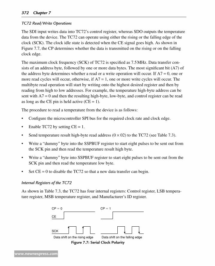
TC72 Read/Write Operations
The SDI input writes data into TC72’s control register, whereas SDO outputs the temperature data from the device. The TC72 can operate using either the rising or the falling edge of the clock (SCK). The clock idle state is detected when the CE signal goes high. As shown in Figure 7.7, the CP determines whether the data is transmitted on the rising or on the falling clock edge.
The maximum clock frequency (SCK) of TC72 is specified as 7.5 MHz. Data transfer con-sists of an address byte, followed by one or more data bytes. The most significant bit (A7) of the address byte determines whether a read or a write operation will occur. If A7 = 0, one or more read cycles will occur, otherwise, if A7 = 1, one or more write cycles will occur. The multibyte read operation will start by writing onto the highest desired register and then by reading from high to low addresses. For example, the temperature high-byte address can be sent with A7 = 0 and then the resulting high-byte, low-byte, and control register can be read as long as the CE pin is held active (CE = 1).
The procedure to read a temperature from the device is as follows:
Configure the microcontroller SPI bus for the required clock rate and clock edge. •
Enable TC72 by setting CE • = 1.
Send temperature result high-byte read address (0 • × 02) to the TC72 (see Table 7.3).
Write a “dummy” byte into • the SSPBUF register to start eight pulses to be sent out from the SCK pin and then read the temperature result high byte.
Write a “dummy” byte into SSPBUF register to start eight pulses to be sent out from the •SCK pin and then read the temperature low byte.
Set CE • = 0 to disable the TC72 so that a new data transfer can begin.
Internal Registers of the TC72
As shown in Table 7.3, the TC72 has four internal registers: Control register, LSB tempera-ture register, MSB temperature register, and Manufacturer’s ID register.
Figure 7.7: Serial Clock Polarity
CE
SCK
CP 5 0 CP 5 1
Data shift on the rising edge Data shift on the falling edge
372 Chapter 7
www.newnespress.com

Control Register
The Control register is a read and write register used to select the mode of operation as shut-down, continuous, or OS. The address of this register is 0 × 00 when reading and 0 × 80 when writing onto the device. Table 7.4 shows how different modes are selected. At power-up, the shutdown bit (SHDN) is set to 1 so that the device is in shutdown mode at start-up, and the device is used in this mode to minimize power consumption.
A temperature conversion is initiated by a write operation to the Control register to select either the continuous mode or the OS mode. The temperature data will be available in the MSB and LSB registers after approximately 150 ms of the write operation. The OS mode performs a single temperature measurement, after which time the device returns to the shutdown mode. In continuous mode, new temperature data is available at 159-ms intervals.
LSB and MSB Registers
The LSB and MSB registers are read-only registers that contain the 10-bit measured tempera-ture data. The address of the MSB register is 0 × 02 and that of the LSB register is 0 × 01.
Manufacturer’s ID
The Manufacturer’s ID is a read-only register with address 0 × 03. This register identifies the device as a temperature sensor, returning 0 × 054.
table 7.3: tC72 internal registers
registerread
addressWrite
address Bit 7 Bit 6 Bit 5 Bit 4 Bit 3 Bit 2 Bit 1 Bit 0
Control 0 × 00 0 × 80 0 0 0 OS 0 1 0 SHDN
LSB temperature 0 × 01 N/A T1 T0 0 0 0 0 0 0
MSB temperature 0 × 02 N/A T9 T8 T7 T6 T5 T4 T3 T2
Manufacturer’s ID 0 × 03 N/A 0 1 0 1 0 1 0 0
table 7.4: Selecting the Mode of Operation
Operating Mode One Shot Shutdown (ShdN)
Continuous X 0
Shutdown 0 1
One shot 1 1
serial Peripheral Interface Bus Operation 373
www.newnespress.com

762 The Circuit Diagram
The circuit diagram of the project is shown in Figure 7.8. The TC72 temperature sensor is connected to the SPI bus pins of a PIC18F452 microcontroller, which is operated from a 4-MHz crystal. The CE pin of the TC72 is controlled from pin RC0 of the microcontroller. An LCD is connected to PORTB of the microcontroller in the default configuration, i.e., the connection between the TC72, LCD, and microcontroller is as follows:
Microcontroller LCd
RB0 D4
RB1 D5
RB2 D6
RB3 D7
RB4 E
RB5 R/S
RB6 RW
Microcontroller tC72
RC0 CE
RC3 SCK
RC4 SDO
RC5 SDI
The operation of the project is very simple. The microcontroller sends control commands to the TC72 sensor to initiate the temperature conversions every second. The temperature data is then read and displayed on the LCD.
763 The Program
The program listing of the project is shown in Figure 7.9. The program reads the temperature from the TC72 sensor and displays it on the LCD every second. In this version of the program, only the positive temperatures and only the integer part are displayed.
The program consists of a number of functions. At the beginning of the program, some definitions are made to make the program more readable. The LCD delay routines DelayFor18TCY, DelayPORXLCD, and DelayXLCD are then given for a 4-MHz clock rate. Two further delay routines are also used in the program: Delay200 ms creates a delay of 200 ms and is used during the TC72 temperature conversion routine. One_Second_Delay creates a 1-s delay and is used to read and display the temperature every second.
374 Chapter 7
www.newnespress.com

Figure 7.8: Circuit diagram of the Project
VDD
MCLR
RC0RB6RB5RB4RB0RB1RB2RB3
OSC2
RC3 (SCK)RC5 (SDO)RC4 (SDI)
D4
RSR/W
E
D5D6D7 VSS
VDD VEE
GNDSDO
SCKCEVDD
10 K
TC72 SDI
PIC18F452
LCD
VssTemperature sensor 12
31
13 14
23241815
25242315161718
5
2 3
46
11121314
1
5632
8
4
1
11 32
15 V
4 MHz resonator
OSC1
/******************************************************************************************************************************** SPI BUS–BASED DIGITAL THERMOMETER ================================
In this project, a TC72-type SPI bus–based temperature sensor IC is used.The IC is connected to the SPI bus pins of a PIC18F452 type microcontroller(i.e., to pins RC3 = SCK, RC4 = SDI, and RC5 = SDO) and the microcontroller isoperated from a 4-MHz resonator.
In addition, PORT B pins of the microcontroller are connected to a standardLCD.
The microcontroller reads the temperature every second and displays on theLCD as a positive number (fractional part of the temperature and negativetemperatures are not displayed in this version of the program).
An example display is:
23
Author: Dogan IbrahimDate: July 2009File: TC72-1.C********************************************************************************************************************************/#include <p18f452.h>#include <spi.h>#include <stdlib.h>#include <xlcd.h>#include <delays.h>
Figure 7.9: Program Listing of the Project
serial Peripheral Interface Bus Operation 375
www.newnespress.com

#pragma config WDT = OFF, OSC = XT, LVP = OFF
#define CE PORTCbits.RC0
#define CLR_LCD 1#define HOME_LCD 2
#define Ready SSPSTATbits.BF
unsigned char LSB, MSB;int result;
//// LCD Delays//void DelayFor18TCY(void) // 18 cycle delay Nop( ); Nop( ); Nop( ); Nop( ); Nop( ); Nop( ); Nop( ); Nop( ); Nop( ); Nop( ); Nop( ); Nop( ); Nop( ); Nop( ); return;
void DelayPORXLCD(void) // 15ms Delay Delay1KTCYx(15);
void DelayXLCD(void) // 5ms Delay Delay1KTCYx(5);
//// This function generates 200ms delay for the TC72 conversion//void Delay200ms(void) Delay1KTCYx(200);
//// This function generates 1 second delay//void One_Second_Delay(void) Delay10KTCYx(100);
Figure 7.9: Cont’d
376 Chapter 7
www.newnespress.com
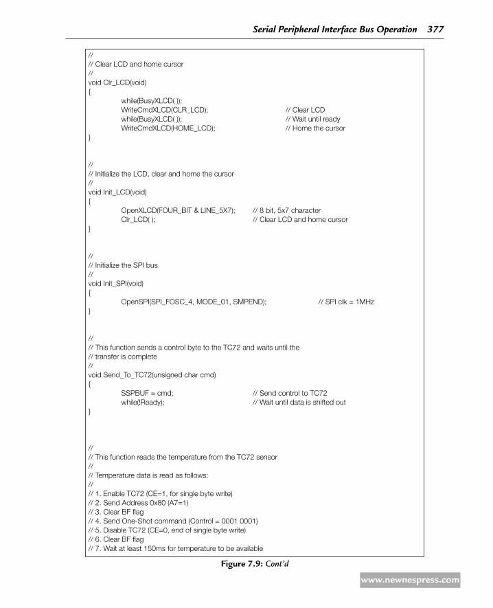
//// Clear LCD and home cursor//void Clr_LCD(void) while(BusyXLCD( )); WriteCmdXLCD(CLR_LCD); // Clear LCD while(BusyXLCD( )); // Wait until ready WriteCmdXLCD(HOME_LCD); // Home the cursor
//// Initialize the LCD, clear and home the cursor//void Init_LCD(void) OpenXLCD(FOUR_BIT & LINE_5X7); // 8 bit, 5x7 character Clr_LCD( ); // Clear LCD and home cursor
//// Initialize the SPI bus//void Init_SPI(void) OpenSPI(SPI_FOSC_4, MODE_01, SMPEND); // SPI clk = 1MHz
//// This function sends a control byte to the TC72 and waits until the// transfer is complete//void Send_To_TC72(unsigned char cmd) SSPBUF = cmd; // Send control to TC72 while(!Ready); // Wait until data is shifted out
//// This function reads the temperature from the TC72 sensor//// Temperature data is read as follows://// 1. Enable TC72 (CE=1, for single byte write)// 2. Send Address 0x80 (A7=1)// 3. Clear BF flag// 4. Send One-Shot command (Control = 0001 0001)// 5. Disable TC72 (CE=0, end of single byte write)// 6. Clear BF flag// 7. Wait at least 150ms for temperature to be available
Figure 7.9: Cont’d
serial Peripheral Interface Bus Operation 377
www.newnespress.com

// 8. Enable TC72 (CE=1, for multiple data transfer)// 9. Send Read MSB command (Read address=0x02)// 10. Clear BF flag// 11. Send dummy output to start clock and read data (Send 0x00)// 12. Read high temperature into variable MSB// 13. Send dummy output to start clock and read data (Send 0x00)// 14. Read low temperature into variable LSB// 15. Disable TC72 data transfer (CE=0)// 16. Copy high result into variable “result”void Read_Temperature(void) char dummy;
CE = 1; // Enable TC72 Send_To_TC72(0x80); // Send control write with A7=1 dummy = SSPBUF; // Clear BF flag Send_To_TC72(0x11); // Set for one-shot operation CE = 0; // Disable TC72 dummy = SSPBUF; // Clear BF flag Delay200ms( ); // Wait 200ms for conversion CE = 1; // Enable TC72 Send_To_TC72(0x02); // Read MSB temperature address dummy = SSPBUF; // Clear BF flag Send_To_TC72(0x00); // Read temperature high byte MSB = SSPBUF; // save temperature and clear BF Send_To_TC72(0x00); // Read temperature low byte LSB = SSPBUF; // Save temperature and clear BF CE = 0; // Disable TC72 result = MSB;
//// This function formats the temperature for displaying on the LCD.// The temperature is read as a byte. We have to convert it to a string// to display on the LCD.//// Only the positive MSB is displayed in this version of the program//void Format_Temperature(char *tmp) itoa(result,tmp); // Convert integer to ASCII
//// This function clears the LCD, homes the cursor and then displays the// temperature on the LCD//void Display_Temperature(char *d) Clr_LCD( ); // Clear LCD and home cursor putsXLCD(d);
Figure 7.9: Cont’d
378 Chapter 7
www.newnespress.com
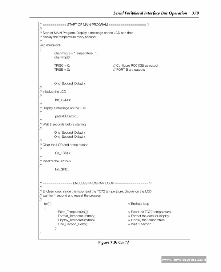
/* ============ START OF MAIN PROGRAM =================== *///// Start of MAIN Program. Display a message on the LCD and then// display the temperature every second//void main(void) char msg[ ] = “Temperature...”; char tmp[3];
TRISC = 0; // Configure RC0 (CE) as output TRISB = 0; // PORT B are outputs
One_Second_Delay( );//// Initialize the LCD// Init_LCD( );//// Display a message on the LCD// putsXLCD(msg);//// Wait 2 seconds before starting// One_Second_Delay( ); One_Second_Delay( );//// Clear the LCD and home cursor// Clr_LCD( );//// Initialize the SPI bus// Init_SPI( );
/* =============== ENDLESS PROGRAM LOOP ================= *///// Endless loop. Inside this loop read the TC72 temperature, display on the LCD,// wait for 1 second and repeat the process// for(;;) // Endless loop Read_Temperature( ); // Read the TC72 temperature Format_Temperature(tmp); // Format the data for display Display_Temperature(tmp); // Display the temperature One_Second_Delay( ); // Wait 1 second
Figure 7.9: Cont’d
serial Peripheral Interface Bus Operation 379
www.newnespress.com

Some other functions used in the program are as follows:
Clr_LCD: This function clears the LCD screen and homes the cursor.
Init_LCD: This function initializes the LCD to 4-bit operation with 5 × 7 characters. The function also calls Clr_LCD to clear the LCD screen and home the cursor.
Init_SPI: This function initializes the microcontroller SPI bus to
Clock rate: Fosc/4 (i.e., 1 MHz)
Clock idle low, shift data on clock falling edge
Input data sample at end of data out.
Send_To_TC72: This function loads a byte to SPI register SSPBUF and then waits until the data is shifted out.
Read_Temperature: This function communicates with the TC72 sensor to read the temperature. The following operations are performed by this function:
1. Enables TC72 (CE = 1, for single-byte write).
2. Sends Address 0 × 80 (A7 = 1).
3. Clears BF flag.
4. Sends OS command (Control = 0001 0001).
5. Disables TC72 (CE = 0, end of single-byte write).
6. Clears BF flag.
7. Waits at least for 150 ms for the temperature to be available.
8. Enables TC72 (CE = 1 for multiple data transfer).
9. Sends Read MSB command (Read address = 0 × 02).
10. Clears BF flag.
11. Sends dummy output to start clock and read data (Send 0 × 00).
12. Reads high temperature into variable MSB.
13. Sends dummy output to start clock and read data (Send 0 × 00).
14. Reads low temperature into variable LSB.
15. Disables TC72 data transfer (CE = 0).
16. Copies high result into variable “result.”
380 Chapter 7
www.newnespress.com

Format_Temperature: This function converts the integer temperature into ASCII string so that it can be displayed on the LCD.
Display_Temperature: This function calls to Clr_LCD to clear the LCD screen and homes the cursor. The temperature is then displayed calling function putsXLCD.
Main Program: At the beginning of the main program, the port directions are configured, LCD is initialized, the message “Temperature…” is sent to the LCD, and the microcontroller SPI bus is initialized. The program then enters an endless loop, where the following functions are called inside this loop:
Read_Temperature();
Format_Temperature(tmp);
Display_Temperature(tmp);
One_Second_Delay();
764 Displaying Negative Temperatures
The program given in Figure 7.9 displays only the positive temperatures. Negative temperatures are stored in TC72 in two’s complement format. If bit 8 of the MSB byte is set, the temperature is negative and two’s complement should be taken to find the correct tem-perature. For example, if the MSB and LSB bytes are “1110 0111/1000 0000,” the correct temperature is
1110 0111/1000 0000 -> the complement is 0001 1000/0111 1111
Adding “1” to find the two’s complement gives 0001 1000/1000 0000,
i.e., the temperature is “−24.5°C.”
Similarly, if the MSB and LSB bytes are “1110 0111/0000 0000,” the correct temperature is
1110 0111/0000 0000 -> the complement is 0001 1000/1111 1111
Adding “1” to find the two’s complement gives 0001 1001/0000 0000,
i.e., the temperature is “−25°C.”
The modified program is shown in Figure 7.10. In this program, both negative and positive temperatures are displayed, and the sign “−” is inserted before the negative temperatures. The temperature is displayed in the integer format with no fractional part in this version of the program.
In this version of the program, the Format_Temperature function is modified such that if the temperature is negative, the two’s complement is taken, the sign bit is inserted,
serial Peripheral Interface Bus Operation 381
www.newnespress.com

and then the value is shifted right by eight digits and converted into an ASCII string for the display.
765 Displaying the Fractional Part
The program in Figure 7.10 displays both the positive and negative temperatures, but it does not display the fractional part of the temperature. The modified program given in Figure 7.11 displays the fractional part as well. The main program is basically the same as that in Figure 7.10, but function Format_Temperature is modified. In the new program, the LSB byte of the converted data is taken into consideration and the fractional part is displayed as “0.00,” “0.25,” “0.50,” or “0.75.” The two most significant bits of the LSB byte are shifted right by 6 bits. The fractional part then takes one of the following values:
two-Shifted LSB Bits Fractional Part
00 0.00
01 0.25
10 0.50
11 0.75
Figure 7.10: Modified Program to display Negative temperatures
/********************************************************************************************************************************** SPI BUS–BASED DIGITAL THERMOMETER ================================
In this project, a TC72 type SPI bus–based temperature sensor IC is used.The IC is connected to the SPI bus pins of a PIC18F452-type microcontroller(i.e., to pins RC3 = SCK, RC4 = SDI, and RC5 = SDO) and the microcontroller isoperated from a 4-MHz resonator.
In addition, PORT B pins of the microcontroller are connected to a standardLCD.
The microcontroller reads the temperature every second and displays it on theLCD as a positive or negative number (fractional part of the temperature isnot displayed in this version of the program).
An example display is:
-25
Author: Dogan IbrahimDate: July 2009File: TC72-2.C*********************************************************************************************************************************/
382 Chapter 7
www.newnespress.com
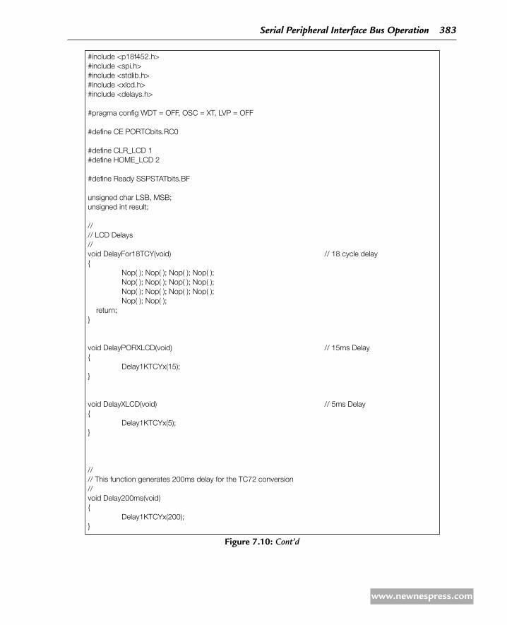
#include <p18f452.h>#include <spi.h>#include <stdlib.h>#include <xlcd.h>#include <delays.h>
#pragma config WDT = OFF, OSC = XT, LVP = OFF
#define CE PORTCbits.RC0
#define CLR_LCD 1#define HOME_LCD 2
#define Ready SSPSTATbits.BF
unsigned char LSB, MSB;unsigned int result;
//// LCD Delays//void DelayFor18TCY(void) // 18 cycle delay Nop( ); Nop( ); Nop( ); Nop( ); Nop( ); Nop( ); Nop( ); Nop( ); Nop( ); Nop( ); Nop( ); Nop( ); Nop( ); Nop( ); return;
void DelayPORXLCD(void) // 15ms Delay Delay1KTCYx(15);
void DelayXLCD(void) // 5ms Delay Delay1KTCYx(5);
//// This function generates 200ms delay for the TC72 conversion//void Delay200ms(void) Delay1KTCYx(200);
Figure 7.10: Cont’d
serial Peripheral Interface Bus Operation 383
www.newnespress.com

//// This function generates 1 second delay//void One_Second_Delay(void) Delay10KTCYx(100);
//// Clear LCD and home cursor//void Clr_LCD(void) while(BusyXLCD( )); WriteCmdXLCD(CLR_LCD); // Clear LCD while(BusyXLCD( )); // Wait until ready WriteCmdXLCD(HOME_LCD); // Home the cursor
//// Initialize the LCD, clear and home the cursor//void Init_LCD(void) OpenXLCD(FOUR_BIT & LINE_5X7); // 8 bit, 5x7 character Clr_LCD( ); // Clear LCD, home cursor
//// Initialize the SPI bus//void Init_SPI(void) OpenSPI(SPI_FOSC_4, MODE_01, SMPEND); // SPI clk = 1MHz
//// This function sends a control byte to the TC72 and waits until the// transfer is complete//void Send_To_TC72(unsigned char cmd) SSPBUF = cmd; // Send control to TC72 while(!Ready); // Wait until shifted out
//// This function reads the temperature from the TC72 sensor
Figure 7.10: Cont’d
384 Chapter 7
www.newnespress.com

Figure 7.10: Cont’d
//// Temperature data is read as follows://// 1. Enable TC72 (CE=1, for single byte write)// 2. Send Address 0x80 (A7=1)// 3. Clear BF flag// 4. Send One-Shot command (Control = 0001 0001)// 5. Disable TC72 (CE=0, end of single byte write)// 6. Clear BF flag// 7. Wait at leat 150ms for temperature to be available// 8. Enable TC72 (CE=1, for multiple data transfer)// 9. Send Read MSB command (Read address=0x02)// 10. Clear BF flag// 11. Send dummy output to start clock and read data (Send 0x00)// 12. Read high temperature into variable MSB// 13. Send dummy output to start clock and read data (Send 0x00)// 14. Read low temperature into variable LSB// 15. Disable TC72 data transfer (CE=0)// 16. Copy high result into variable “result”void Read_Temperature(void) char dummy;
CE = 1; // Enable TC72 Send_To_TC72(0x80); // Send control with A7=1 dummy = SSPBUF; // Clear BF flag Send_To_TC72(0x11); // Set for one-shot operation CE = 0; // Disable TC72 dummy = SSPBUF; // Clear BF flag Delay200ms( ); // Wait 200ms for conversion CE = 1; // Enable TC72 Send_To_TC72(0x02); // Read MSB temperature address dummy = SSPBUF; // Clear BF flag Send_To_TC72(0x00); // Read temperature high byte MSB = SSPBUF; // Save temperature and clear BF Send_To_TC72(0x00); // Read temperature low byte LSB = SSPBUF; // Save temperature and clear BF CE = 0; // Disable TC72 result = MSB*256 + LSB; // The complete temperature
//// This function formats the temperature for displaying on the LCD.// The temperature is read as a byte. We have to convert it to a string// to display on the LCD.//// Positive and negative temperatures are displayed in this version of the program//void Format_Temperature(char *tmp) if(result & 0x8000) // If negative result = ~result; // Take complement
serial Peripheral Interface Bus Operation 385
www.newnespress.com
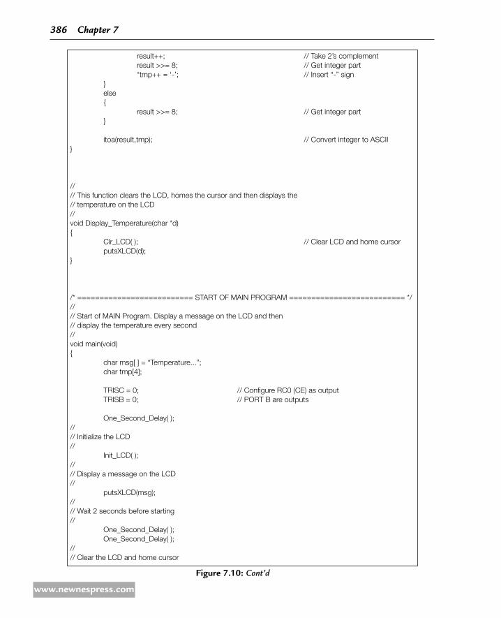
result++; // Take 2’s complement result >>= 8; // Get integer part *tmp++ = ‘-’; // Insert “-” sign else result >>= 8; // Get integer part
itoa(result,tmp); // Convert integer to ASCII
//// This function clears the LCD, homes the cursor and then displays the// temperature on the LCD//void Display_Temperature(char *d) Clr_LCD( ); // Clear LCD and home cursor putsXLCD(d);
/* ========================== START OF MAIN PROGRAM ========================== *///// Start of MAIN Program. Display a message on the LCD and then// display the temperature every second//void main(void) char msg[ ] = “Temperature...”; char tmp[4];
TRISC = 0; // Configure RC0 (CE) as output TRISB = 0; // PORT B are outputs
One_Second_Delay( );//// Initialize the LCD// Init_LCD( );//// Display a message on the LCD// putsXLCD(msg);//// Wait 2 seconds before starting// One_Second_Delay( ); One_Second_Delay( );//// Clear the LCD and home cursor
Figure 7.10: Cont’d
386 Chapter 7
www.newnespress.com

// Clr_LCD( );//// Initialize the SPI bus// Init_SPI( );
/* ========================== ENDLESS PROGRAM LOOP ========================== *///// Endless loop. Inside this loop, read the TC72 temperature, display on the LCD,// wait for 1 second and repeat the process// for(;;) // Endless loop Read_Temperature( ); // Read the TC72 temperature Format_Temperature(tmp); // Format the data for display Display_Temperature(tmp); // Display the temperature One_Second_Delay( ); // Wait 1 second
Figure 7.10: Cont’d
/****************************************************************************************************************************************** SPI BUS–BASED DIGITAL THERMOMETER ================================
In this project, a TC72-type SPI bus–based temperature sensor IC is used.The IC is connected to the SPI bus pins of a PIC18F452-type microcontroller(i.e., to pins RC3 = SCK, RC4 = SDI, and RC5 = SDO) and the microcontroller isoperated from a 4-MHz resonator.
In addition, PORT B pins of the microcontroller are connected to a standardLCD.
The microcontroller reads the temperature every second and displays it on theLCD as a positive or negative number. The fractional part of the temperature isdisplayed as 2 digits in this version of the program.
An example display is:
-25.75
Author: Dogan IbrahimDate: July 2009File: TC72-3.C******************************************************************************************************************************************/#include <p18f452.h>#include <spi.h>#include <stdlib.h>#include <xlcd.h>#include <delays.h>
Figure 7.11: Modified Program to display Fractional Part as Well
serial Peripheral Interface Bus Operation 387
www.newnespress.com

#pragma config WDT = OFF, OSC = XT, LVP = OFF
#define CE PORTCbits.RC0
#define CLR_LCD 1#define HOME_LCD 2
#define Ready SSPSTATbits.BF
unsigned char LSB, MSB;unsigned int result, int_part, fract_part;
//// LCD Delays//void DelayFor18TCY(void) // 18 cycle delay Nop( ); Nop( ); Nop( ); Nop( ); Nop( ); Nop( ); Nop( ); Nop( ); Nop( ); Nop( ); Nop( ); Nop( ); Nop( ); Nop( ); return;
void DelayPORXLCD(void) // 15ms Delay Delay1KTCYx(15);
void DelayXLCD(void) // 5ms Delay Delay1KTCYx(5);
//// This function generates 200ms delay for the TC72 conversion//void Delay200ms(void) Delay1KTCYx(200);
//// This function generates 1 second delay//void One_Second_Delay(void) Delay10KTCYx(100);
Figure 7.11: Cont’d
388 Chapter 7
www.newnespress.com
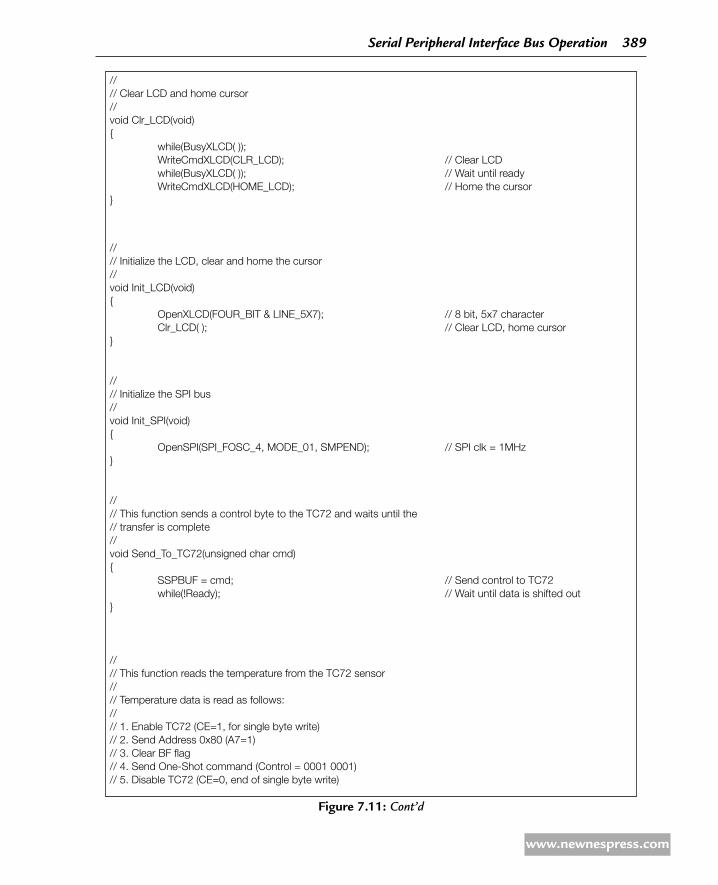
//// Clear LCD and home cursor//void Clr_LCD(void) while(BusyXLCD( )); WriteCmdXLCD(CLR_LCD); // Clear LCD while(BusyXLCD( )); // Wait until ready WriteCmdXLCD(HOME_LCD); // Home the cursor
//// Initialize the LCD, clear and home the cursor//void Init_LCD(void) OpenXLCD(FOUR_BIT & LINE_5X7); // 8 bit, 5x7 character Clr_LCD( ); // Clear LCD, home cursor
//// Initialize the SPI bus//void Init_SPI(void) OpenSPI(SPI_FOSC_4, MODE_01, SMPEND); // SPI clk = 1MHz
//// This function sends a control byte to the TC72 and waits until the// transfer is complete//void Send_To_TC72(unsigned char cmd) SSPBUF = cmd; // Send control to TC72 while(!Ready); // Wait until data is shifted out
//// This function reads the temperature from the TC72 sensor//// Temperature data is read as follows://// 1. Enable TC72 (CE=1, for single byte write)// 2. Send Address 0x80 (A7=1)// 3. Clear BF flag// 4. Send One-Shot command (Control = 0001 0001)// 5. Disable TC72 (CE=0, end of single byte write)
Figure 7.11: Cont’d
serial Peripheral Interface Bus Operation 389
www.newnespress.com

// 6. Clear BF flag// 7. Wait at leat 150ms for temperature to be available// 8. Enable TC72 (CE=1, for multiple data transfer)// 9. Send Read MSB command (Read address=0x02)// 10. Clear BF flag// 11. Send dummy output to start clock and read data (Send 0x00)// 12. Read high temperature into variable MSB// 13. Send dummy output to start clock and read data (Send 0x00)// 14. Read low temperature into variable LSB// 15. Disable TC72 data transfer (CE=0)// 16. Copy high result into variable “result”void Read_Temperature(void) char dummy;
CE = 1; // Enable TC72 Send_To_TC72(0x80); // Send control write with A7=1 dummy = SSPBUF; // Clear BF flag Send_To_TC72(0x11); // Set for one-shot operation CE = 0; // Disable TC72 dummy = SSPBUF; // Clear BF flag Delay200ms( ); // Wait 200ms for conversion CE = 1; // Enable TC72 Send_To_TC72(0x02); // Read MSB temperature address dummy = SSPBUF; // Clear BF flag Send_To_TC72(0x00); // Read temperature high byte MSB = SSPBUF; // Save temperature and clear BF Send_To_TC72(0x00); // Read temperature low byte LSB = SSPBUF; // Save temperature and clear BF CE = 0; // Disable TC72 result = MSB*256 + LSB; // The complete temperature
//// This function formats the temperature for displaying on the LCD.// The temperature is read as a byte. We have to convert it to a string// to display on the LCD.//// Positive and negative temperatures are displayed in this version of the program//void Format_Temperature(char *tmp) if(result & 0x8000) // If negative result = ~result; // Take complement result++; // Take 2’s complement int_part = result >> 8; // Get integer part *tmp++ = ‘-’; // Insert “-” sign else int_part = result >> 8; // Get integer part
Figure 7.11: Cont’d
390 Chapter 7
www.newnespress.com

//// Convert integer part to ASCII string// itoa(int_part,tmp); // Convert integer to ASCII
//// Now find the fractional part. First we must find the end of the string “tmp”// and then append the fractional part to it// while(*tmp !=‘\0’)tmp++; // find end of string “tmp”//// Now add the fractional part as “.00”, “.25”, “.50”, or “.75”// fract_part = result &0x00C0; // fractional part fract_part = fract_part >> 6; // fract is between 0-3 switch(fract_part) case 1: // Fractional part = 0.25 *tmp++ = ‘.’; // decimal point *tmp++ = ‘2’; // “2” *tmp++ = ‘5’; // “5” break; case 2: // Fractional part = 0.50 *tmp++ = ‘.’; // decimal point *tmp++ = ‘5’; // “5” *tmp++ = ‘0’; // “0” break; case 3: // Fractional part = 0.75 *tmp++ = ‘.’; // decimal point *tmp++ = ‘7’; // “7” *tmp++ = ‘5’; // “5” break; case 0: // Fractional part = 0.00 *tmp++ = ‘.’; // decimal point *tmp++ = ‘0’; // “0” *tmp++ = ‘0’; // “0” break; *tmp++ = ‘\0’; // Null terminator
//// This function clears the LCD, homes the cursor and then displays the// temperature on the LCD//void Display_Temperature(char *d) Clr_LCD( ); // Clear LCD and home cursor putsXLCD(d);
Figure 7.11: Cont’d
serial Peripheral Interface Bus Operation 391
www.newnespress.com

/* ================ START OF MAIN PROGRAM ================ *///// Start of MAIN Program. Display a message on the LCD and then display the// temperature every second//void main(void) char msg[ ] = “Temperature...”; char tmp[8];
TRISC = 0; // Configure RC0 (CE) as output TRISB = 0; // PORT B are outputs
One_Second_Delay( );//// Initialize the LCD// Init_LCD( );//// Display a message on the LCD// putsXLCD(msg);//// Wait 2 seconds before starting// One_Second_Delay( ); One_Second_Delay( );//// Clear the LCD and home cursor// Clr_LCD( );//// Initialize the SPI bus// Init_SPI( );
/* ============================ ENDLESS PROGRAM LOOP============================ *///// Endless loop. Inside this loop, read the TC72 temperature, display on the LCD,// wait for 1 second and repeat the process// for(;;) // Endless loop Read_Temperature( ); // Read the TC72 temperature Format_Temperature(tmp); // Format the data for display Display_Temperature(tmp); // Display the temperature One_Second_Delay( ); // Wait 1 second
Figure 7.11: Cont’d
392 Chapter 7
www.newnespress.com

7.7 Summary
In this chapter, the properties of the SPI bus and how it can be used in the PIC microcontroller circuits are described. An example is given to show how the SPI bus can be used to read the temperature from an SPI bus–compatible temperature sensor device.
7.8 exercisesWhat are the operating modes of the MSSP module? 1.
Which pins are used in the SPI mode? Describe the function of each pin. 2.
Describe the SPI mode registers in detail. How can the MSSP be configured to operate in 3. SPI mode?
Explain in detail, by drawing a diagram, how data can be sent and received by a master 4. SPI device.
It is required to operate the MSSP device of a PIC microcontroller in SPI mode. The 5. data should be shifted on rising edge of the clock and the SCK signal must be idle low. The required data rate is at least 2 Mbps. Assume that the microcontroller clock rate is 32 MHz and the input data is to be sampled at the middle of data output time. What should be the settings of the MSSP registers?
Describe which MPLAB C18 library functions can be used to read and write to an SPI 6. device.
The MSB and LSB registers of a TC72 sensor contain the following bits. What is the 7. temperature reading?
MSB: 00111101LSB: 11000000
Modify the program given in Figure 7.9 to display the temperature as a 2-digit integer 8. number between 0 and 99 on a pair of seven-segment displays.
serial Peripheral Interface Bus Operation 393
www.newnespress.com

This page intentionally left blank

© 2010 Elsevier Ltd. All rights reserved.D.O.I.: 10.1016/B978-1-85617-719-1.00012-9
ChaPter 8
MPLAB C18 sD Card Functions and Procedures
Reading and writing onto secure digital (SD) cards is a complex process and requires the development of a number of rather complex functions and procedures to handle the card I/O operations correctly.
Fortunately, Microchip Inc. provides a library of file I/O functions for implementing the card file operations. This library is named “Microchip MDD File system,” where MDD stands for “memory disk drive.” The library can be downloaded free of charge from the Microchip Web site. The library is based on the ISO/IEC 9293 specifications and supports the MPLAB C18 and MPLAB C30 compilers. The library can be used for
FAT16 and FAT32 file systems. FAT16 is • an earlier file system usually found in MSDOS-based systems and early Windows systems. The current Windows operating systems (e.g., Windows XP) support both FAT16 and FAT32 file systems. SD cards (and multimedia cards) up to 2 GB use the FAT16 standard filing system. The FAT32 filing system is used for higher-capacity SD cards, usually between 2 GB and 2 TB.
The MDD library supports SD cards, compact flash cards, and USB thumb drives. •
In this book, we shall be looking at how to install the MDD library and how to use the library functions and procedures in the PIC18 series of microcontrollers, using the MPLAB C18 compiler (further information about the MDD library can be obtained from the Microchip application note AN1045, Document no: DS01045B, entitled “Implementing File I/O Func-tions Using Microchip’s Memory Disk Drive File System Library.”)
8.1 installation of the Mdd Library
The current version (at the time of writing this book) of the Microchip MDD library has the filename “Microchip MDD File System 1.2.1 Installer.exe.” The library can be installed by the following steps:
Download the library from Microchip Web site •
Double-click the file and follow the instructions to load •
395

The MDD library creates a directory called “Microchip Solutions” under the • “C:\” root directory. The following directories are created and files are copied to the “Microchip Solutions” directory:
Directory: “MDD File System-SD Card” contains demonstration programs for the PIC18, PIC24, and PIC32 microcontrollers.
Directory: “MDD File System-SD Data Logger” contains an example SD card data logging application.
Directory: “Microchip” contains various common files, help files, include files, and documentation files.
8.2 Mdd Library Functions821 File and Disk Manipulation Functions
The MDD library provides a large number of “File and Disk Manipulation” functions that can be called and used from MPLAB C18 programs. The functions can be placed under the following groups:
Initialize a card •
Open/create/close/delete/locate/rename a file on the card •
Read/write to an opened file •
Create/delete/change/rename a directory on the card •
Format a card •
Set file creation and modification date and time •
The summary of each function is given briefly in Tables 8.1–8.6.
822 Library Options
A number of options are available in the MDD library. These options are enabled or disabled by uncommenting or commenting them, respectively, in include file FSconfig.h. The avail-able options are given in Table 8.7.
table 8.1: initialize a Card Function
Functions descriptions
FSInit Initialize the card
396 Chapter 8
www.newnespress.com

MPLAB C18 sD Card Functions and Procedures 397
table 8.3: read/Write Functions
Functions descriptions
FSfread Reads data from an open file to a buffer
FSfwrite Writes data from a buffer onto an open file
FSftell Returns the current position in a file
FSfprintf Writes a formatted string onto a file
table 8.4: Create/delete/Change/rename directory
Functions descriptions
FSmkdir Creates a new subdirectory in the current woking directory
FSrmdir Deletes the specified directory
FSchdir Changes the current working directory
FSrename Changes the name of a directory
FSgetcwd Returns name of the current working directory
table 8.5: Format a Card
Function description
FSformat Formats a card
table 8.2: Open/Create/Close/delete/Locate/rename Functions
Functions descriptions
FSfopen/FSfopenpgm Opens an existing file for reading or for appending at the end of the file or creates a new file for writing.
FSfclose Updates and closes a file. The file time-stamping information is also updated
FSRemove/FSremovepgm Deletes a file
FSrename Changes the name of a file
FindFirst/FindFirstpgm Locates a file in the current directory that matches the specified name and attributes
FindNext Locates the next file in the current directory that matches the name and attributes specified earlier
…pgm versions are to be used with the PIC18 microcontrollers where the arguments are specified in ROM.
table 8.6: File time-Stamping Function
Function description
SetClockVars Sets the date and time that will be applied to files when they are created or modified
www.newnespress.com
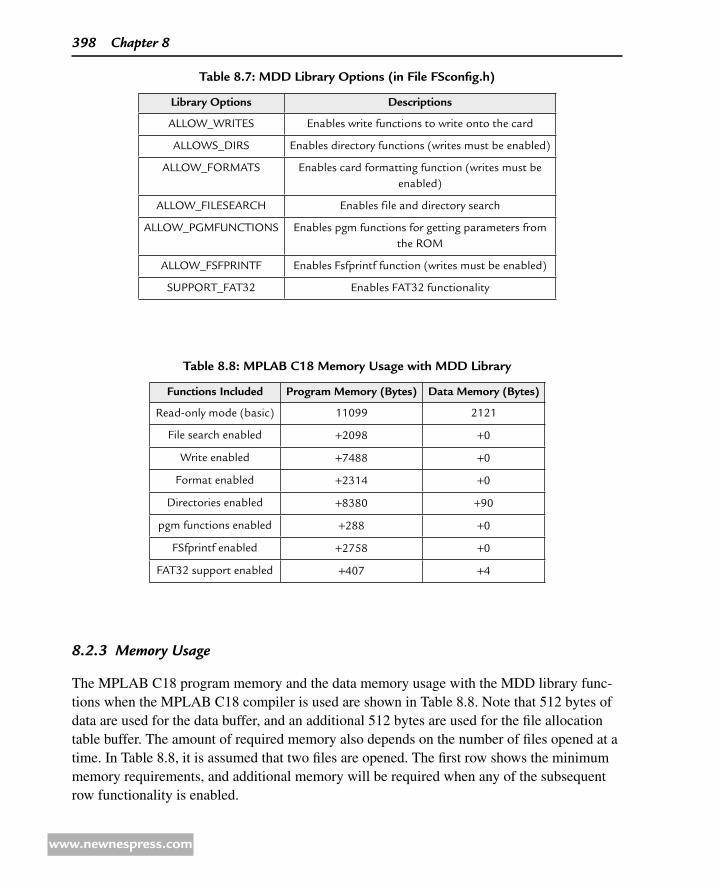
table 8.7: Mdd Library Options (in File FSconfig.h)
Library Options descriptions
ALLOW_WRITES Enables write functions to write onto the card
ALLOWS_DIRS Enables directory functions (writes must be enabled)
ALLOW_FORMATS Enables card formatting function (writes must be enabled)
ALLOW_FILESEARCH Enables file and directory search
ALLOW_PGMFUNCTIONS Enables pgm functions for getting parameters from the ROM
ALLOW_FSFPRINTF Enables Fsfprintf function (writes must be enabled)
SUPPORT_FAT32 Enables FAT32 functionality
823 Memory Usage
The MPLAB C18 program memory and the data memory usage with the MDD library func-tions when the MPLAB C18 compiler is used are shown in Table 8.8. Note that 512 bytes of data are used for the data buffer, and an additional 512 bytes are used for the file allocation table buffer. The amount of required memory also depends on the number of files opened at a time. In Table 8.8, it is assumed that two files are opened. The first row shows the minimum memory requirements, and additional memory will be required when any of the subsequent row functionality is enabled.
table 8.8: MPLaB C18 Memory Usage with Mdd Library
Functions included Program Memory (Bytes) data Memory (Bytes)
Read-only mode (basic) 11099 2121
File search enabled +2098 +0
Write enabled +7488 +0
Format enabled +2314 +0
Directories enabled +8380 +90
pgm functions enabled +288 +0
FSfprintf enabled +2758 +0
FAT32 support enabled +407 +4
398 Chapter 8
www.newnespress.com

824 Library setup
There are a number of header files that should be customized before compiling a project (see Chapter 9 for details). These files and the type of customization that can be done are given below (it is assumed that we will be using dynamic memory allocation in the filing system):
File • FSConfig.h can be modified to change
The maximum number of files open at any time (the default is 2)1.
FAT sector size (the default is 512 bytes)2.
Library options. The defaults are (comment the ones not required to save code space):3.
ALLOW_FILESEARCH
ALLOW_WRITES
ALLOW_DIRS
ALLOW_PGMFUNCTIONS
SUPPORT_FAT32
USERDEFINEDCLOCK
File • HardwareProfile.h can be modified
1. to change system clock (the default is 4 MHz)
2. to enable SD-SPI interface. The default is
USE_SD_INTERFACE_WITH_SPI
3. to define SD card interface pins. The defaults are
SD chip select (SD_CS) -> RB3
SD card detect (SD_CD) -> RB4
SD write enable (SD_WE) -> RA4
SPI clock (SPICLOCKPORT) -> RC3
SPI input (SPIINPORT) -> RC4
SPI output (SPIOUTPORT) -> RC5
(If any of the above is changed, then the corresponding TRIS registers must also be changed accordingly.)
MPLAB C18 sD Card Functions and Procedures 399
www.newnespress.com

Configure main SPI control registers. The defaults are4.
SPICON1 -> SSP1CON1
SPISTAT -> SSP1STAT
SPIBUF -> SSP1BUF
SPISTAT_RBF -> SSP1STATbits.BF
SPICON1bits -> SSP1CON1bits
SPISTATbits -> SSP1STATbits
SPI_INTERRUPT_FLAG -> PIR1bits.SSPIF
SPIENABLE -> SPICON1bits.SSPEN
Make sure that all the I/O pins used in the SD card interface are configured as digital I/O •(and not as analog I/O)
Modify the linker file to include a 512-byte section of RAM to act as a buffer for file read •and write operations. In addition, create a section in the linker called dataBuffer that maps to this RAM.
Modify the linker file to include a 512-byte section of RAM to act as a buffer for read and •write of FAT. In addition, create a section in the linker called FATBuffer that maps to this RAM.
Select the appropriate microcontroller definition file at the beginning of your program. •
8.3 Sequence of Function Calls
The sequence of function calls to read or write data onto a file or to delete an existing file is given in this section.
831 Reading from an Existing File
The steps to open an existing file and read from it are
Call FSInit to initialize the card and SPI bus
Call FSfopen or FSfopenpgm to open the existing file in read mode
Call FSfread to read data from the file
Call FSfclose to close the file
The FSread function can be called as many times as required.
400 Chapter 8
www.newnespress.com

832 Writing Onto an Existing File
The steps to open an existing file and append data to it are
Call FSInit to initialize the card and SPI bus
Call FSfopen or FSfopenpgm to open the existing file in append mode
Call FSwrite to write data onto the file
Call FSfclose to close the file
The FSwrite function can be called as many times as required.
833 Deleting an Existing File
The steps to delete an existing file are
Call FSInit to initialize the card and SPI bus
Call FSfopen or FSfopenpgm to open the existing file in write mode
Call FSremove or FSremovepgm to delete the file
Call FSfclose to close the file
8.4 detailed Function Calls
This section gives a detailed description of the Microchip file and disk manipulation functions (further information can be obtained from the Microchip Application Note: AN1045, Docu-ment no: DS01045B). The functions return and its typical use are shown with a simple call to each function. The functions are given in the order of typical use, i.e., initializing, opening, reading, writing, deleting, renaming, directories, and so on.
841 FsInit
This function initializes the SPI bus and mounts the SD card, and it must be called before any other MDD functions are called. The function returns an integer status. If the card is detected and the card is formatted with FAT12/FAT16 or FAT32, then TRUE is returned, otherwise a FALSE is returned.
The following example shows how this function can be called:
if(FSInit( ) == FALSE)//// Failed to initialize
MPLAB C18 sD Card Functions and Procedures 401
www.newnespress.com

The low-level function MediaIsPresent() can be used to check whether or not the card is present. If the card is removed, FSInit must be called again to remount the card.
842 Fsfopen
This function opens a file on the SD card and associates a file structure with it. The function has two parameters: the filename and the mode.
The filename must be NULL terminated and must be less than eight characters, followed by a dot “.” and a three-character file-extension name. The filename must be stored in RAM memory; thus, it should be declared as a character string.
The mode is a NULL-terminated one-character string that specifies the mode of access. The mode must be stored in RAM memory. Some of the valid modes are
r Read-only
w Write (a new file is created if it already exists)
w+ Create a new file (read and writes are enabled)
a Append (if the file exists, any writing will be appended to the end of the file. If the file does not
exist, a new file will be created)
The function returns a file structure or a NULL if the file could not be opened.
The following example shows how this function can be called to open a new file called “MYFILE.DAT”:
FSFILE * MyFile;char FileName[11] = “MYFILE.DAT”;char FileMode[2] = “w+”;MyFile = FSfopen(Filename, FileMode);
843 Fsfopenpgm
This function opens a file on the SD card and associates a file structure with it. The function has two parameters: the filename and the mode.
The filename must be NULL terminated and must be less than eight characters, followed by a dot “.” and a three-character file-extension name. The filename must be stored in ROM memory; thus, the filename can be entered directly as a string in the function.
402 Chapter 8
www.newnespress.com

The mode is a NULL-terminated one-character string that specifies the mode of access. The mode must be stored in the ROM memory. Valid modes are
r Read-only
w Write (a new file is created if it already exists)
w+ Create a new file (read and writes are enabled)
a Append (if the file exists, any writing will be appended to the end of the File. If the file does not
exist, a new file will be created)
The function returns a file structure or a NULL if the file could not be opened.
The following example shows how this function can be called to open a new file called “MYFILE.DAT”:
FSFILE * MyFile;MyFile = FSfopenpgm(“MYFILE.DAT”, “w+”);
844 Fsfclose
This function is called to close an opened file. The function returns an integer 0 if the file is closed successfully or a −1 (EOF) if the file failed to close. A pointer to the opened file (obtained from a previous call to FSopen) must be specified as the argument.
The following example shows how an opened file can be closed:
if(FSfclose(MyFile) == 0)//// File closed successfully
845 Fsfeof
This function detects whether end-of-file is reached while reading from a file. A pointer to the opened file must be specified as the argument. The function returns an integer 1 (EOF) if the end-of-file is reached, otherwise 0 is returned. A pointer to the opened file must be specified as the argument.
The following example shows how the end-of-file can be detected:
if(FSfeof(MyFile) == EOF)//// end-of-file detected
MPLAB C18 sD Card Functions and Procedures 403
www.newnespress.com

846 Fsfread
This function reads n bytes of data, each of length size bytes from the opened file and copies the data to the buffer pointed to by the buffer pointer.
The following parameters are required:
pntr Pointer to the buffer that is to hold the data
size Length of each item (bytes)
n Number of items to read
ptr Pointer to the opened file
pntr Pointer to the buffer where data is to be written
size Length of each item (bytes)
n Number of items to read
ptr Pointer to the opened file
The total number of bytes read is actually n*size.
The function returns the number of items read or a 0 if there is an error in transferring n*size bytes.
The following example shows how 20 packets of size 10 bytes each can be read and trans-ferred to a buffer pointed to by pntr:
count = FSfread(pntr, 10, 20, MyFile);
In the above example, if the transfer is successful, count stores the total number of items actually read from the card. The possibilities are:
count == 0 // no data was read from the cardcount < 20 // could not read 20 packets (EOF, or other error)count == 20 // all 20 packets have been read
847 Fsfwrite
This function writes n bytes of data, each of length size bytes, from a buffer pointed to by pntr to a previously opened file.
The following parameters are required:
The total number of bytes read is actually n*size.
The function returns the number of items read or 0 if there is an error in transferring n*size bytes.
404 Chapter 8
www.newnespress.com

The following example shows how 20 packets of size 10 bytes each can be written from a buffer pointed to by pntr to the card:
count = FSfwrite(pntr, 10, 20, MyFile);
In the above example, if the transfer is successful, count stores the total number of items actually written to the card. The possibilities are
count == 0 // no data was written to the cardcount < 20 // could not write 20 packetscount == 20 // all 20 packets have been written
848 Fsremove
This function deletes a file from the current directory. The filename must be specified in the RAM.
The function returns 0 if the deletion is successful or −1 on failure.
The following example shows how the file named “MYFILE.DAT” can be deleted:
char FileName[12] = “MYFILE.DAT”;if(FSremove(FileName) == 0)//// file deleted successfully
849 Fsremovepgm
This function deletes a file from the current directory. The filename must be specified in the ROM, i.e., the filename can be directly entered as a string to the function.
The function returns 0 if the deletion is successful, or −1 on failure.
The following example shows how the file named “MYFILE.DAT” can be deleted:
if(FSremovepgm(“MYFILE.DAT”) == 0)//// file deleted successfully
8410 Fsrewind
This function sets the file pointer to the beginning of the file. The file structure opened earlier must be specified as an argument to the function. The function does not return anything.
A typical call to this function is
FSrewind(MyFile);
8411 Fsmkdir
This function creates a directory where the directory path string must be passed as an argument to the function. Directory names must be eight ASCII characters or less and must be delimited
MPLAB C18 sD Card Functions and Procedures 405
www.newnespress.com
by the backslash character “\”. The standard MSDOS “dot” formatting is used, where a dot “.” accesses the current directory and two dots “..” access the previous directory. A directory in the “root directory” is created by specifying a backslash “\” before the directory name.
If the directory creation is successful, 0 is returned, otherwise −1 is returned.
In the following example, a directory called “COUNTS” will be created in the current directory:
char DirPath[ ] = “\COUNTS”;if(!FSmkdir(DirPath))//// directory created successfully
8412 Fsrmdir
This function deletes a directory where the directory path string must be passed as an argument to the function. Directory names must be eight ASCII characters or less and must be delimited by the backslash character “\”. The standard MSDOS “dot” formatting is used, where a dot “.” accesses the current directory and two dots “..” access the previous directory. A directory in the “root directory” is accessed by specifying a backslash “\” before the directory name.
The function requires two arguments: the directory path name and the mode. If the mode is TRUE, all subdirectories and files will be deleted. If the mode is FALSE, the directory will be deleted only if it is empty.
The function returns 0 on success and −1 if it fails to delete the directory.
In the following example, the directory called “COUNTS” in the current directory will be deleted. In addition, all the files within this directory will also be deleted:
char DirPath[ ] = “\COUNTS”;if(FSrmdir(DirPath, TRUE) == 0)//// directory and all its files deleted successfully
8413 Fschdir
This function changes the current default directory. Directory names must be eight ASCII characters or less and must be delimited by the backslash character “\”. The standard MSDOS “dot” formatting is used, where a dot “.” accesses the current directory and two dots “..” access the previous directory. A directory in the “root directory” is accessed by specifying a backslash “\” before the directory name.
The path of the directory to be changed to must be specified as an argument to the function.
The function returns 0 on success and −1 if it fails to change the default working directory.
406 Chapter 8
www.newnespress.com

In the following example, the working directory is changed to “NUMBERS”:
char NewDir[ ] = “\NUMBERS”;if(FSchdir(NewDir == 0)//// directory changed successfully
8414 Fsformat
This function deletes the FAT and root directory of a card. A new boot sector will be created if required. The function only supports FAT16 formatting.
The function has three arguments:
mode
0 erases the FAT and root directory
1 creates a new master boot sector (MBR must be present)
serno Serial number to write into the new boot sector
volume Volume ID of the card (up to eight characters)
The function returns 0 if the formatting is successful, otherwise −1 is returned.
In the following example, an SD card is formatted and a new boot sector is created. The card volume name is set to “LOGS,” and the card serial number is set to hexadecimal 0x11223344:
char CardVol[ ] = “LOGS”;if(FSformat(1, 0x11223344, CardVol) == 0)//// card formatted successfully
8415 Fsrename
This function changes the name of a file or a directory. The new filename and the name of the file to be changed must be specified as arguments to the function. If a NULL is passed as a pointer, then the name of the current working directory will be changed.
The function returns 0 if the filename is changed, otherwise −1 is returned.
In the following example, the name of the file pointed to by structure ptr will be changed to “NEW.DAT”:
FSFILE *ptr;if(FSrename(“NEW.DAT”, ptr) == 0)//// filename changed successfully
MPLAB C18 sD Card Functions and Procedures 407
www.newnespress.com

8416 FindFirst
This function finds the first file in the current directory that matches the specified filename and file attribute criteria passed in the arguments.
The function has three arguments:
table 8.9: Filename Formats
Format description
*.* Any file or directory
FILE.EXT File with name FILE.EXT
FILE.* Any file with name FILE and any extension
*.EXT Any file with any name and extension EXT
* Any directory
DIRS Directory names DIRS
table 8.10: File attributes (Can Be Logically Or’ed)
attribute description
ATTR_READ_ONLY Files with read-only attribute
ATTR_HIDDEN Hidden files
ATTR_SYSTEM System files
ATTR_VOLUME File may be a volume label
ATTR_DIRECTORY File may be a directory
ATTR_ARCHIVE File with archive attribute
ATTR_MASK File with any attribute
filename The filename that must match (see Table 8.9)
attr The file attribute that must match (see Table 8.10)
rec Pointer to a structure of type Searchrec that will contain the file information if the file is found
(see Table 8.11)
The function returns 0 if a match is found, otherwise −1 is returned.
408 Chapter 8
www.newnespress.com

In the following example, files starting with “MY” and having extensions “.TXT” are searched in the current directory. The attribute field is set to hidden or system files:
SearchRec MyFile;unsigned char attr = ATTR_HIDDEN | ATTR_SYSTEM;char FileName[ ] = “MY*.TXT”;if(FindFirst(FileName, attr, &MyFile) == 0)//// file match found
Note that after a file match is found, we can get information about the file using the function SearchRec. For example, the full name of the file can be obtained using MyFile.filename or the file size can be obtained using MyFile.size.
8417 FindFirstpgm
This function is very similar to FindFirst, except that the filename must be specified in ROM.
In the following example, files starting with “MY” and having extensions “.TXT” are searched in the current directory. The attribute is set to hidden or system files:
SearchRec MyFile;unsigned char attr = ATTR_HIDDEN | ATTR_SYSTEM;if(FindFirst(“MY*.TXT”, attr, &MyFile) == 0)//// file match found
table 8.11: the Searchrec Structure
Member Function
Char filename Name of the file (NULL terminated)
Unsigned char attributes File attributes
Unsigned long size Size of files (bytes)
Unsigned long time-stamp File creation date and time: 31:25 Year (0 = 1980, 1 = 1981,....) 24–21 Month (1 = Jan, 2 = Feb,...)
20:16 Day (1–31) 15:11 Hours (0–23)
10:05 Minutes (0–59) 04:00 Seconds/2 (0–29)
Unsigned int entry Internal use only
Char search name Internal use only
Unsigned char search attr Internal use only
Unsigned int cwd clus Internal use only
Unsigned char initialized Internal use only
MPLAB C18 sD Card Functions and Procedures 409
www.newnespress.com

8418 FindNext
This function matches the next file in the current directory to the filename and attribute cri-teria specified by the last call to Findfirst (or FindFirstpgm).
The pointer to a SearchRec structure must be specified as an argument. The function returns 0 if a match is found, otherwise −1 is returned.
In the following example, a second match is found to a previously specified filename and attribute criteria (here, it is assumed that a FindFirst function call was made earlier):
if(FindNext(&MyFile) == 0)//// second match is found
8419 setClockVars
This function is used when the user-defined Clock mode is selected, and the function sets the timing variables used to set file creation and modification times.
The following arguments must be specified when the function is called:
Year The current year (1980–2107)
Month The current month (1–12)
Day The current day (1–31)
Hour The current hour (0–23)
Minute The current minute (0–59)
Second The current second (0–59)
The function returns 0 on success and −1 if one or more parameters are invalid.
In the example given below, the date and time are set to July 10, 2009, 11:30:10 a.m.
if(SetClockVars(2009, 7, 10, 11, 30, 10) == 0)//// date and time set successfully
8420 Fsfprintf
This function writes a formatted string to a file opened on a card. The function is similar to the standard fprintf statement. The first argument is a pointer to the file, the second argument is the string to write to (must be specified in ROM), and the other arguments are the format specifiers.
The function returns the number of bytes written on success or −1 if the write failed.
410 Chapter 8
www.newnespress.com
The format specifiers are similar to that used in standard fprintf statements and are normally written in the following order:
Flag characters, field width, field precision, size specification, and conversion specifiers. Further details on format specifiers can be obtained from the Microchip Application note: AN1045 (Implementing File I/O Functions Using Microchip’s Memory Disk Drive File System Library).
An example is given below:
FSfprintf(ptr, "Binary number=%#16b", 0x1eff);
The output will be:
Binary number=0b0001111011111111
8.5 Summary
In this chapter, the MDD functions available for reading and writing onto SD cards using the MPLAB C18 compiler are described. The use of SD cards in microcontroller-based projects is highly simplified when these functions are used.
8.6 exercises
1. Explain the steps required to read and write onto an SD card using the MDD library functions.
2. Assume that a text file called “DATA.TXT” exists on an SD card. It is required to create a new file called “NEW.TXT” on the card and copy the first 100 bytes from “DATA.TXT” to “NEW.TXT.” Show the steps required to perform this operation.
3. It is required to find out how many files with extensions “.TXT” are there in the current default working directory of an SD card. Show the steps required to perform this operation.
4. Assume that a file called “MONTHLY.DAT” exists on an SD card. Show the steps required to change the name of this file to “MONTH2.DAT.”
5. Show the steps required to delete a file on an SD card.
6. Show the steps required to find out how many files with names “TEMP” there are in the working default directory of an SD card and show how this number can be displayed on an LCD.
7. It is required to find the names and sizes of all the files in the current working directory of an SD card. Show how this information can be found and stored in a buffer in RAM.
MPLAB C18 sD Card Functions and Procedures 411
www.newnespress.com

8. Assume that a text file called “MYDATA.TXT” exists in the current directory. Show the steps required to create a new directory called NEWD in the current directory, and also show how the file can be copied to this new directory.
9. Show the steps required to delete a directory called “DIRS” and all of its contents. Assume that this directory is in the current working directory.
10. It is required to find out the number of files in the current directory with the system attribute. Show the steps required to perform this operation, and also show how the number found can be displayed on an LCD.
11. Show the steps required to format and create a new boot sector on an SD card. Give the volume name “MYSD” and serial number 0x87654321 to the formatted card.
12. It is required to delete all the files in the current directory of an SD card. Show the steps required to perform this operation.
13. Explain what happens when an SD card is removed from its socket. How can we find out whether or not the card is mounted?
412 Chapter 8
www.newnespress.com

© 2010 Elsevier Ltd. All rights reserved.D.O.I.: 10.1016/B978-1-85617-719-1.00013-0
ChaPter 9
secure Digital Card Projects
The details of the Microchip memory disk drive (MDD) library, which consist of a large number of MPLAB C18 compiler–compatible functions that can be used in secure digital (SD) card-based projects, are given in Chapter 8.
In this chapter, we shall be looking at how these functions can actually be used in practical projects. The many simple-to-complex projects given in this chapter show how SD card-based projects can be built and how an SD card can be used as a large external storage medium.
The projects have been organized by increasing level of complexity. Thus, it is advised that the reader start from Project 1 and then move to more complex projects as experience is gained.
The following information is given for each project:
Description of the project •
Aim of the project •
Block diagram of the project •
Circuit diagram of the project •
Operation of the project •
Program code of the project •
Description of the program code •
Suggestions for future work •
The projects can be built using most of the commercially available PIC18 microcontroller development boards. Alternatively, complete projects can be built on a breadboard of suitable size. It is recommended to use an external +5-V power supply to provide power to the micro-controller and the associated circuitry used in the projects. Alternatively, a 9-V battery and a 7805 type +5-V regulator can be used to supply power to the projects.
In this book, the PICDEM PIC18 Explorer demonstration board (see Figure 9.1) is used for the projects. As described in Chapter 5, this development board has been specifically
413

designed for PIC18-based applications. The board incorporates a PIC18F8722-type microcontroller operating with a 10-MHz clock. The board has the following features:
Connector for external daughter boards (e.g., SD card board) •
LCD display •
Eight LEDs •
Analog temperature sensor •
Push-button switches •
RS232 socket for serial communications •
External reset button •
Potentiometer for analog inputs •
Figure 9.1: PiCdeM PiC18 explorer demonstration Board
414 Chapter 9
www.newnespress.com
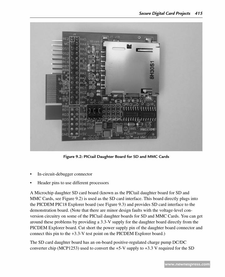
In-circuit-debugger connector •
Header pins to use different processors •
A Microchip daughter SD card board (known as the PICtail daughter board for SD and MMC Cards, see Figure 9.2) is used as the SD card interface. This board directly plugs into the PICDEM PIC18 Explorer board (see Figure 9.3) and provides SD card interface to the demonstration board. (Note that there are minor design faults with the voltage-level con-version circuitry on some of the PICtail daughter boards for SD and MMC Cards. You can get around these problems by providing a 3.3-V supply for the daughter board directly from the PICDEM Explorer board. Cut short the power supply pin of the daughter board connector and connect this pin to the +3.3-V test point on the PICDEM Explorer board.)
The SD card daughter board has an on-board positive-regulated charge pump DC/DC converter chip (MCP1253) used to convert the +5-V supply to +3.3 V required for the SD
Figure 9.2: PiCtail daughter Board for Sd and MMC Cards
secure Digital Card Projects 415
www.newnespress.com

card. In addition, the board has buffers to provide correct voltages for the SD card inputs. Seven jumpers are provided on the board to select the SD card signal interface. The following jumpers should be selected:
Figure 9.3: the daughter Board Plugs onto the PiCdeM Board
Jumpers descriptions
JPI Pin 1-2 SCK connected to RC3
JP2 Pin 1-2 SDI connected to RC4
JP3 Pin 1-2 SDO connected to RC5
JP4 Pin 2-3 (default) Card detect to RB4 (not used)
JP5 Pin 2-3 (default) Write protect to RA4 (not used)
JP6 Pin 2-3 (default) CS connected to RB3
JP7 Pin 2-3 (default) Shutdown (not used)
The default jumper positions are connected by circuit tracks on the board, and these tracks should be cut to change the jumper positions if different connections are desired. Signals “card detect,” “write protect,” and “shutdown” are not used in this book, and the jumper settings can be left as they are.
416 Chapter 9
www.newnespress.com

Before starting the programming, make sure that you have a suitable programming device that can program the PIC18 series of microcontrollers. In addition, you will require a copy of the MPLAB C18 compiler and a copy of the Microchip MDD library. In this book, the ICD3 in-circuit-debugger device is used to program the PICDEM Explorer board.
9.1 Creating an MPLaB C18 template
In this section, we shall be creating an MPLAB C18 template that can be used in all of our SD card projects. The template will be based on using the PIC18F8722 microcontroller with the MDD library. The steps are given below:
Start the MPLAB and select Project -> Project Wizard (see Figure 9.4) •
Click Next and select the processor type as PIC18F8722 (see Figure 9.5) •
Click Next. Select Microchip C18 Toolsuite. Make sure that the tool suite components •point to the correct directories (see Figure 9.6):
MPASM assembler (mpasmwin.exe) -> C:\MCC18\mpasm\mpasmwin.exe
MPLINK Object Linker (mplink.exe) -> C:\MCC18\bin\mplink.exe
MPLAB C18 C Compiler (mcc18.exe)-> C:\MCC18\bin\mcc18.exe
MPLIB Librarian (mplib.exe) -> C:\MCC18\bin\mplib.exe
Figure 9.4: Start the Project Wizard
secure Digital Card Projects 417
www.newnespress.com

Figure 9.5: Select the Processor type
Figure 9.6: Check the C18 toolsuite Components
418 Chapter 9
www.newnespress.com

Click Next. Create a new project called SD_CARD_PROJECTS in directory C:\ •Microchip Solutions\MDD File System-SD Card. That is, enter C:\Microchip Solutions\MDD File System-SD Card\SD_CARD_PROJECTS (see Figure 9.7). You can click the Browse to find the directory, and then enter the filename and click Save button. Click Next to create the project file.
Open the Notepad and create a text file called FIRST.C. Save this file in directory C:\ •Microchip Solutions\MDD File System-SD Card. This will be your template source file. The contents of this file should be as shown in Figure 9.8.
Click Next. Click the following files on the left-hand side and click Add to add them to •the project (see Figure 9.9):
C:\Microchip Solutions\Microchip\MDD File System\FSIO.c
C:\Microchip Solutions\Microchip\MDD File System\SD-SPI.c
C:\Microchip Solutions\Microchip\PIC18 salloc\salloc.c
C:\Microchip Solutions\Microchip\Include\Compiler.h
C:\Microchip Solutions\Microchip\Include\GenericTypeDefs.h
C:\Microchip Solutions\MDD File System-SD Card\Pic18f\FSconfig.h
Figure 9.7: Create a New Project Sd_Card_PrOJeCtS
secure Digital Card Projects 419
www.newnespress.com

/**********************************************************************************************************
PROJECT TO WRITE SHORT TEXT TO AN SD CARD=========================================
In these projects, a PIC18F8722-type microcontroller is used. The microcontroller is operated with a 10-MHz crystal.
An SD card is connected to the microcontroller as follows:
SD card microcontrollerCS RB3CLK RC3DO RC4DI RC5
The program uses the Microchip MDD library functions to read and write to the SD card.
*************************** Insert other comments here ****************************
Author: Dogan IbrahimDate: July 2009File: write filename here**********************************************************************************************************/#include <p18f8722.h>#include <FSIO.h>
#pragma config WDT = OFF, OSC = HSPLL, LVP = OFF#pragma config MCLRE = ON, CCP2MX = PORTC, MODE = MC
/* =================== START OF MAIN PROGRAM =================== *///// Start of MAIN Program//void main(void)
//// Initialize the SD card routines//
FSInit( );
//// Other code here//
Figure 9.8: template Source File
420 Chapter 9
www.newnespress.com

Figure 9.9: adding Files to the Project
C:\Microchip Solutions\MDD File System-SD Card\Pic18f\HardwareProfile.h
C:\Microchip Solutions\Microchip\Include\MDD File System\FSDefs.h
C:\Microchip Solutions\Microchip\Include\MDD File System\SD-SPI.h
C:\Microchip Solutions\Microchip\Include\MDD File System\FSIO.h
C:\Microchip Solutions\Microchip\Include\PIC18 salloc\salloc.h
Click Next. Click Finish to complete (see Figure 9.10) •
Specify the MDD header include files in the project. Click Project -> Build Options -> •Project (see Figure 9.11)
Select Include Search Path in Show directories for textbox and enter the following •directory names (click New before entering a new set of data), see Figure 9.12:
C:\mcc18\h.\Pic18f..\Microchip\Include..\Microchip\Include\MDD File System...\Microchip\Include\PIC18 salloc..\Microchip\PIC18 salloc
secure Digital Card Projects 421
www.newnespress.com

Figure 9.10: Click Finish to complete
Figure 9.11: Open the Project Folder
422 Chapter 9
www.newnespress.com

Select Library Search Path in Show directories for textbox; click New and enter the •following directory name (see Figure 9.13):
C:\mcc18\lib
Click OK. Click File -> Save Workspace and then File -> Exit to exit from MPLAB after •saving it.
The compiler linker file must be modified to include a 512-byte section for the data read-write and also a 512-byte section for the FAT allocation. This is done by editing the linker file 18f8722.lkr in folder c:\mcc18\lkr and adding lines for a dataBuffer and an FATBuffer. In addition, it is required to add a section named _SRAM_ALLOC_HEAP to the linker file. The modified linker file is shown in Figure 9.14.
We can now verify if everything has been setup correctly.
Restart MPLAB. Select Project -> Open and select SD_CARD_PROJECTS. Click Open. •Double-click on program file FIRST.C. The project file should now open.
Compile the program by clicking Build All. The program should compile and link with •no errors.
Figure 9.12: enter the include Search Path
secure Digital Card Projects 423
www.newnespress.com

Figure 9.13: enter the Library Search Path
911 setting the Configuration Files
It is now necessary to customize some of the header files for our requirements. You should make the following modifications when using the PICDEM PIC18 Explorer demonstration board with the PICtail SD card daughter board (you are recommended to make copies of the original files before modifying them, in case you ever want to return to them):
Modify the file C:\Microchip Solutions\MDD File System-SD Card\Pic18f\FSconfig.h •and enable the following defines:
1. #define FS_MAX_FILES_OPEN 2
2. #define MEDIA_SECTOR_SIZE 512
3. #define ALLOW_FILESEARCH #define ALLOW_WRITES
424 Chapter 9
www.newnespress.com
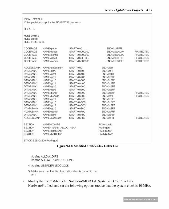
#define ALLOW_DIRS #define ALLOW_PGMFUNCTIONS
4. #define USERDEFINEDCLOCK
5. Make sure that the file object allocation is dynamic. i.e. #if 1
Modify the file C:\Microchip Solutions\MDD File System-SD Card\Pic18f \ •HardwareProfile.h and set the following options (notice that the system clock is 10 MHz,
// File: 18f8722.lkr// Sample linker script for the PIC18F8722 processor
LIBPATH .
FILES c018i.oFILES clib.libFILES p18f8722.lib
CODEPAGE NAME=page START=0x0 END=0x1FFFFCODEPAGE NAME=idlocs START=0x200000 END=0x200007 PROTECTEDCODEPAGE NAME=config START=0x300000 END=0x30000D PROTECTEDCODEPAGE NAME=devid START=0x3FFFFE END=0x3FFFFF PROTECTEDCODEPAGE NAME=eedata START=0xF00000 END=0xF003FF PROTECTED
ACCESSBANK NAME=accessram START=0x0 END=0x5FDATABANK NAME=gpr0 START=0x60 END=0xFFDATABANK NAME=gpr1 START=0x100 END=0x1FFDATABANK NAME=gpr2 START=0x200 END=0x2FFDATABANK NAME=gpr3 START=0x300 END=0x3FFDATABANK NAME=gpr4 START=0x400 END=0x4FFDATABANK NAME=gpr5 START=0x500 END=0x5FFDATABANK NAME=gpr6 START=0x600 END=0x6FFDATABANK NAME=buffer1 START=0x700 END=0x8FF PROTECTEDDATABANK NAME=buffer2 START=0x900 END=0xAFF PROTECTEDDATABANK NAME=gpr7 START=0xB00 END=0xBFFDATABANK NAME=gpr8 START=0xC00 END=0xCFFDATABANK NAME=gpr9 START=0xD00 END=0xEFF//DATABANK NAME=gpr9 START=0xE00 END=0xEFF//DATABANK NAME=gpr10 START=0xF00 END=0xFFFDATABANK NAME=gpr11 START=0xF00 END=0xF5FACCESSBANK NAME=accesssfr START=0xF60 END=0xFFF PROTECTED
SECTION NAME=CONFIG ROM=configSECTION NAME=_SRAM_ALLOC_HEAP RAM=gpr7SECTION NAME=dataBuffer RAM=buffer1SECTION NAME=FATBuffer RAM=buffer2
STACK SIZE=0x200 RAM=gpr9
Figure 9.14: Modified 18f8722.lnk Linker File
secure Digital Card Projects 425
www.newnespress.com
but the configuration option OSC = HSPLL is used to multiply the clock by a factor of four, and it should be set to 40 MHz):
Set clock rate to 40 MHz:1.
#define GetSystemClock( ) 40000000
Enable SD-SPI interface.2.
#define USE_SD_INTERFACE_WITH_SPI
Define SD card interface pins and SPI bus pins to be used:3.
#define SD_CS PORTBBits.RB3 #define SD_CS_TRIS TRISBBits.TRISB3 #define SD_CD PORTBBits.RB4 #define SD_CD_TRIS TRISBBits.TRISB4 #define SD_WE PORTABits.RA4 #define SD_WE_TRIS TRISABits.TRISA4
#define SPICON1 SSP1CON1 #define SPISTAT SSP1STAT #define SPIBUF SSP1BUF #define SPISTAT_RBF SSP1STATbits.BF #define SPICON1bits SSP1CON1bits #define SPISTATbits SSP1STATbits
#define SPICLOCK TRISCbits.TRISC3 #define SPIIN TRISCbits.TRISC4 #define SPIOUT TRISCbits.TRISC5
#define SPICLOCKLAT LATCbits.LATC3 #define SPIINLAT LATCbits.LATC4 #define SPIOUTLAT LATCbits.LATC5
#define SPICLOCKPORT PORTCbits.RC3 #define SPIINPORT PORTCbits.RC4 #define SPIOUTPORT PORTCbits.RC5
912 The Memory Model
The memory model should now be selected correctly. Select Project -> Build Option -> Project; then click the MPLAB C18 tab and select Memory Model in Categories. Set the following options (see Figure 9.15):
Code Model: Large code model
Data Model: Large data model
426 Chapter 9
www.newnespress.com
Stack Model: Multibank model
We are now ready to develop projects using the created template file and the working environment.
9.2 PrOJeCt 1 – Writing a Short text Message to an Sd Card
921 Description
In this project, a file called “MESSAGE.TXT” is created on an SD card and the following short text message is written to this file:
“This is a TEXT message”
922 Aim
The aim of this project is to familiarize the reader with the minimum hardware required to build an SD card-based project. In addition, the configuration of the MDD library and the MPLAB C18 compiler are described so that the reader can compile and build the basic software for an SD card-based project. With the knowledge gained in this project, the reader should be able to move to more complex SD card-based projects.
Figure 9.15: Setting the Memory Model
secure Digital Card Projects 427
www.newnespress.com
923 Block Diagram
The block diagram of the project is shown in Figure 9.16. The hardware setup is very simple. Basically, the microcontroller I/O ports are connected to an SD card using a card holder.
924 Circuit Diagram
The complete circuit diagram of the project is shown in Figure 9.17. In the actual implemen-tation, the PICDEM Explorer demonstration board is used together with the PICtail SD card daughter board. The circuit given in Figure 9.17 can be built on a breadboard if you do not have the PICDEM demonstration board or the SD card daughter board.
The circuit is built around a PIC18F8722-type microcontroller operated from a 10-MHz crystal. The MCLR input is connected to an external push-button switch for external reset of the microcontroller.
The interface between the microcontroller and the SD card pins is as follows. (The card adapter on the PICtail daughter board provides two additional signals: card detect [CD] and write enable [WE].)
Figure 9.16: Block diagram of the Project
PICmicro-
controller
SD card
Sd Card Pins Microcontroller Pins
CS RB3
CLK RC3
DO RC4
DI RC5
The maximum allowable input voltage at the inputs of an SD card is +3.6 V. The voltage at the outputs of the microcontroller is about +4.3 V, which is too high for the inputs (CS, DO, CLK) of the SD card. As a result, potential divider resistors are used to lower the voltage to acceptable levels (on the PICDEM board, buffers are used to lower the voltage levels). With the 2.2- and 3.3-K resistors, the voltage at the inputs of the SD card will be
SD card input voltage = 4.3 V × 3.3 K/(2.2 K + 3.3 K) = 2.48 V
428 Chapter 9
www.newnespress.com
In Figure 9.17, the +3.3-V power for the SD card is derived from a MC33269DT-3.3 type regulator (see Figure 9.18) powered from the +5-V power. (On the PICtail SD card daughter board, an MCP1253 type DC/DC converter is used to provide the +3.3-V supply for the SD card.)
925 Operation of the Project
The operation of the project is very simple and can be described by the program description language (PDL) given in Figure 9.19.
926 Program Code
The program code (file WRITE1.C) is shown in Figure 9.20.
Figure 9.17: Circuit diagram of the Project
Reset
3.3 V
10 mF
SD card
4
VDDCS
CLK
DO
DI
3,6
1 2.2 KRB3
RC3
RC4
RC5
OSC1
10 MHz
22 pF 22 pF
OSC2
Vss
70
51
2611
55
44
45
46
49 50
2.2 K
5
7
2
3.3 K 3.3 K
VSS
1
MC33269DT-3.3
10 K
15 V
12
9
25 32
Vdd
MCLR
PIC18F8722
48 71
secure Digital Card Projects 429
www.newnespress.com
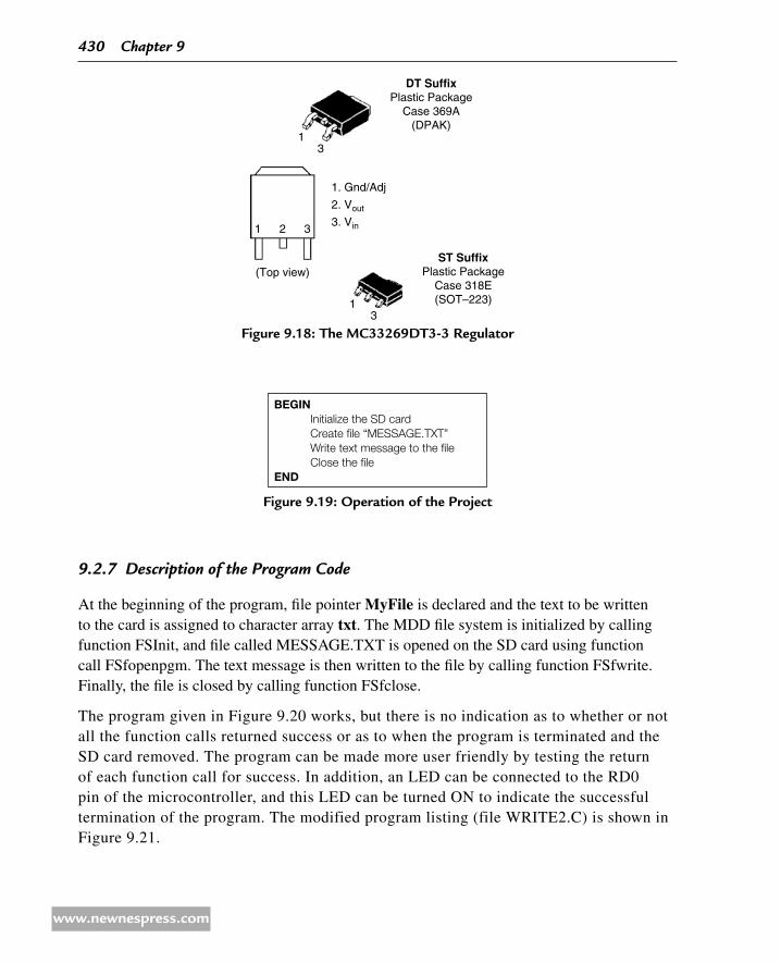
927 Description of the Program Code
At the beginning of the program, file pointer MyFile is declared and the text to be written to the card is assigned to character array txt. The MDD file system is initialized by calling function FSInit, and file called MESSAGE.TXT is opened on the SD card using function call FSfopenpgm. The text message is then written to the file by calling function FSfwrite. Finally, the file is closed by calling function FSfclose.
The program given in Figure 9.20 works, but there is no indication as to whether or not all the function calls returned success or as to when the program is terminated and the SD card removed. The program can be made more user friendly by testing the return of each function call for success. In addition, an LED can be connected to the RD0 pin of the microcontroller, and this LED can be turned ON to indicate the successful termination of the program. The modified program listing (file WRITE2.C) is shown in Figure 9.21.
Figure 9.18: the MC33269dt3-3 regulator
1 2
13
13
(Top view)
DT SuffixPlastic Package
Case 369A(DPAK)
ST SuffixPlastic Package
Case 318E(SOT–223)
1. Gnd/Adj
2. Vout
3. Vin3
Figure 9.19: Operation of the Project
BEGIN Initialize the SD card Create file “MESSAGE.TXT” Write text message to the file Close the fileEND
430 Chapter 9
www.newnespress.com

Figure 9.20: the Program Code
/*************************************************************************************************** PROJECT TO WRITE SHORT TEXT TO AN SD CARD ======================================
In these projects, a PIC18F8722-type microcontroller is used. The microcontrolleris operated with a 10-MHz crystal.
An SD card is connected to the microcontroller as follows:
SD card microcontrollerCS RB3CLK RC3DO RC4DI RC5
The program uses the Microchip MDD library functions to read and write tothe SD card.
Author: Dogan IbrahimDate: July 2009File: WRITE1.C***************************************************************************************************/#include <p18f8722.h>#include <FSIO.h>
#pragma config WDT = OFF, OSC = HSPLL, LVP = OFF#pragma config MCLRE = ON, CCP2MX = PORTC, MODE = MC
/* ================= START OF MAIN PROGRAM ================= *///// Start of MAIN Program//void main(void) FSFILE *MyFile; unsigned char txt[ ]="This is a TEXT message";//// Initialize the SD card routines// FSInit( );//// Create a new file called MESSAGE.TXT// MyFile = FSfopenpgm("MESSAGE.TXT", "w+");//// Write message to the file// FSfwrite(txt, 1, 22, MyFile);//
secure Digital Card Projects 431
www.newnespress.com

// Close the file// FSfclose(MyFile);
while(1);
Figure 9.20: Cont’d
Figure 9.21: Modified Program Code
/*************************************************************************************************** PROJECT TO WRITE SHORT TEXT TO AN SD CARD ======================================
In these projects, a PIC18F8722-type microcontroller is used. The microcontrolleris operated with a 10-MHz crystal.
An SD card is connected to the microcontroller as follows:
SD card microcontrollerCS RB3CLK RC3DO RC4DI RC5
The program uses the Microchip MDD library functions to read and write tothe SD card.
In this version of the program an LED is connected to port RD0 andthe LED is turned ON when the program is terminated successfully.
Author: Dogan IbrahimDate: July 2009File: WRITE2.C***************************************************************************************************/#include <p18f8722.h>#include <FSIO.h>
#pragma config WDT = OFF, OSC = HSPLL, LVP = OFF#pragma config MCLRE = ON, CCP2MX = PORTC, MODE = MC
#define LED PORTDbits.RD0#define ON 1#define OFF 0
/* ================ START OF MAIN PROGRAM ================ *///// Start of MAIN Program//
432 Chapter 9
www.newnespress.com

void main(void) FSFILE *MyFile; unsigned char txt[ ]="This is a TEXT message";
TRISD = 0; PORTD = 0;//// Initialize the SD card routines// while(!FSInit( ));//// Create a new file called MESSAGE.TXT// MyFile = FSfopenpgm("MESSAGE.TXT", "w+"); if(MyFile == NULL)while(1);//// Write message to the file// if(FSfwrite((void *)txt, 1, 22, MyFile) != 22)while(1);//// Close the file// if(FSfclose(MyFile) != 0)while(1);//// Success. Turn ON the LED// LED = ON;
while(1);
Figure 9.21: Cont’d
928 suggestions for Future Work
The programs given in Figures 9.20 and 9.21 can be improved using several LEDs to indicate the cause of the error if the program does not terminate. Alternatively, an LCD can be used to show the status of the program and the cause of any errors.
9.3 PrOJeCt 2 – time Stamping a File
931 Description
In this project, a file called TIME.TXT is created and the following text is written into the file:
The date is 10-July-2009, time is 10:12:05.
The file creation date is set to July 10, 2009, time 10:12:05.
Turn ON the LED connected to port RD0 when the program terminates.
secure Digital Card Projects 433
www.newnespress.com
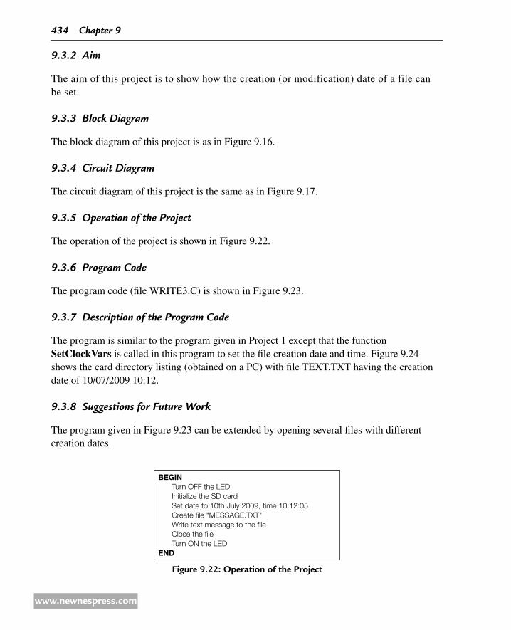
932 Aim
The aim of this project is to show how the creation (or modification) date of a file can be set.
933 Block Diagram
The block diagram of this project is as in Figure 9.16.
934 Circuit Diagram
The circuit diagram of this project is the same as in Figure 9.17.
935 Operation of the Project
The operation of the project is shown in Figure 9.22.
936 Program Code
The program code (file WRITE3.C) is shown in Figure 9.23.
937 Description of the Program Code
The program is similar to the program given in Project 1 except that the function SetClockVars is called in this program to set the file creation date and time. Figure 9.24 shows the card directory listing (obtained on a PC) with file TEXT.TXT having the creation date of 10/07/2009 10:12.
938 suggestions for Future Work
The program given in Figure 9.23 can be extended by opening several files with different creation dates.
BEGIN Turn OFF the LED Initialize the SD card Set date to 10th July 2009, time 10:12:05 Create file "MESSAGE.TXT" Write text message to the file Close the file Turn ON the LEDEND
Figure 9.22: Operation of the Project
434 Chapter 9
www.newnespress.com

/***************************************************************************************************PROJECT TO TIME STAMP A FILE=========================
In these projects, a PIC18F8722-type microcontroller is used. The microcontrolleris operated with a 10-MHz crystal.
An SD card is connected to the microcontroller as follows:
SD card microcontrollerCS RB3CLK RC3DO RC4DI RC5
The program uses the Microchip MDD library functions to read and write tothe SD card.
In this program a new file called TIME.TXT is created and its creation date isset to 10th of July 2009, 10:12:05
Author: Dogan IbrahimDate: July 2009File: WRITE3.C**************************************************************************************************/#include <p18f8722.h>#include <FSIO.h>
#pragma config WDT = OFF, OSC = HSPLL,LVP = OFF#pragma config MCLRE = ON,CCP2MX = PORTC, MODE = MC
#define LED PORTDbits.RD0#define ON 1#define OFF 0
/* ================= START OF MAIN PROGRAM ================ *///// Start of MAIN Program//void main(void) FSFILE *MyFile; unsigned char txt[ ]="The date is 10-July-2009, time is 10:12:05";
TRISD = 0; PORTD = 0;//// Initialize the SD card routines// while(!FSInit( ));//
Figure 9.23: Program Code
secure Digital Card Projects 435
www.newnespress.com
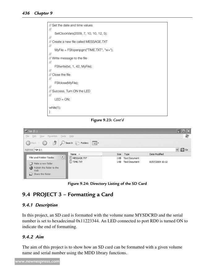
// Set the date and time values// SetClockVars(2009, 7, 10, 10, 12, 5);//// Create a new file called MESSAGE.TXT// MyFile = FSfopenpgm("TIME.TXT", "w+");//// Write message to the file// FSfwrite(txt, 1, 42, MyFile);//// Close the file// FSfclose(MyFile);//// Success. Turn ON the LED// LED = ON;
while(1);
Figure 9.23: Cont’d
9.4 PrOJeCt 3 – Formatting a Card
941 Description
In this project, an SD card is formatted with the volume name MYSDCRD and the serial number is set to hexadecimal 0x11223344. An LED connected to port RD0 is turned ON to indicate the end of formatting.
942 Aim
The aim of this project is to show how an SD card can be formatted with a given volume name and serial number using the MDD library functions.
Figure 9.24: directory Listing of the Sd Card
436 Chapter 9
www.newnespress.com
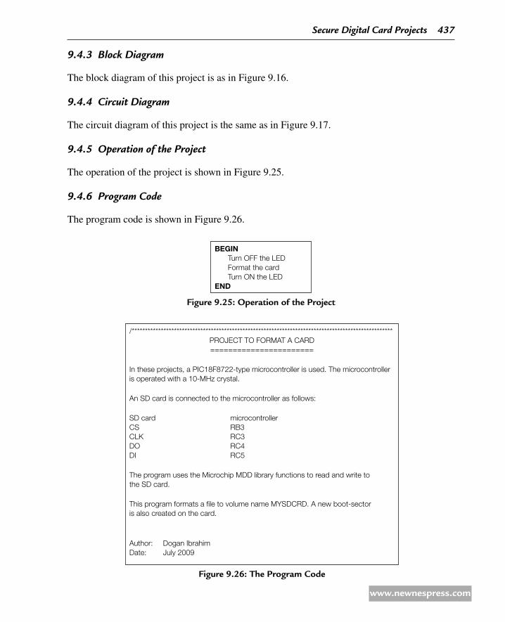
943 Block Diagram
The block diagram of this project is as in Figure 9.16.
944 Circuit Diagram
The circuit diagram of this project is the same as in Figure 9.17.
945 Operation of the Project
The operation of the project is shown in Figure 9.25.
946 Program Code
The program code is shown in Figure 9.26.
BEGIN Turn OFF the LED Format the card Turn ON the LEDEND
Figure 9.25: Operation of the Project
/***************************************************************************************************PROJECT TO FORMAT A CARD=======================
In these projects, a PIC18F8722-type microcontroller is used. The microcontrolleris operated with a 10-MHz crystal.
An SD card is connected to the microcontroller as follows:
SD card microcontrollerCS RB3CLK RC3DO RC4DI RC5
The program uses the Microchip MDD library functions to read and write tothe SD card.
This program formats a file to volume name MYSDCRD. A new boot-sectoris also created on the card.
Author: Dogan IbrahimDate: July 2009
Figure 9.26: the Program Code
secure Digital Card Projects 437
www.newnespress.com

File: FORMAT.C**************************************************************************************************/#include <p18f8722.h>#include <FSIO.h>
#pragma config WDT = OFF, OSC = HSPLL,LVP = OFF#pragma config MCLRE = ON,CCP2MX = PORTC, MODE = MC
#define LED PORTDbits.RD0#define ON 1#define OFF 0
/* =============== START OF MAIN PROGRAM ================== *///// Start of MAIN Program//void main(void) char VolName[ ] = "MYSDCRD";
TRISD = 0; PORTD = 0;//// Format the card// FSformat(0, 0x11223344, VolName);//// Success. Turn ON the LED// LED = ON;
while(1);
Figure 9.26: Cont’d
947 Description of the Program Code
The program simply calls function FSformat to format the card. Notice that the entries #define ALLOW_FORMATS, #define ALLOW_DIRS, and #define ALLOW_WRITES must be enabled in configuration file FSconfig.h
948 suggestions for Future Work
Try formatting different cards with different volume names.
438 Chapter 9
www.newnespress.com
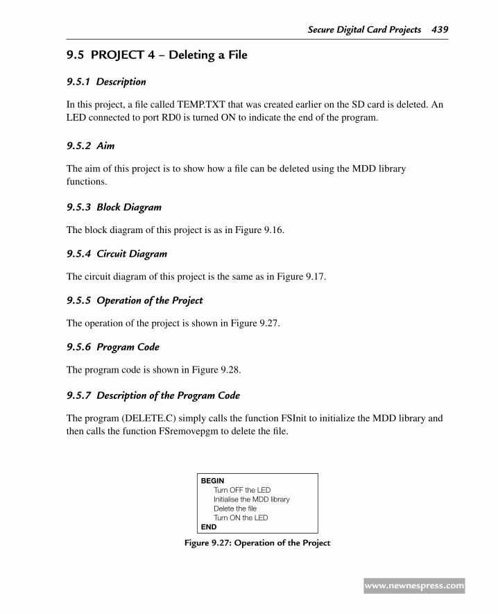
9.5 PrOJeCt 4 – deleting a File
951 Description
In this project, a file called TEMP.TXT that was created earlier on the SD card is deleted. An LED connected to port RD0 is turned ON to indicate the end of the program.
952 Aim
The aim of this project is to show how a file can be deleted using the MDD library functions.
953 Block Diagram
The block diagram of this project is as in Figure 9.16.
954 Circuit Diagram
The circuit diagram of this project is the same as in Figure 9.17.
955 Operation of the Project
The operation of the project is shown in Figure 9.27.
956 Program Code
The program code is shown in Figure 9.28.
957 Description of the Program Code
The program (DELETE.C) simply calls the function FSInit to initialize the MDD library and then calls the function FSremovepgm to delete the file.
BEGIN Turn OFF the LED Initialise the MDD library Delete the file Turn ON the LEDEND
Figure 9.27: Operation of the Project
secure Digital Card Projects 439
www.newnespress.com

/**************************************************************************************************PROJECT TO DELETE A FILE======================
In these projects, a PIC18F8722-type microcontroller is used. The microcontrolleris operated with a 10-MHz crystal.
An SD card is connected to the microcontroller as follows:
SD card microcontrollerCS RB3CLK RC3DO RC4DI RC5
The program uses the Microchip MDD library functions to read and write tothe SD card.
This program deletes file called TEMP.TXT
Author: Dogan IbrahimDate: July 2009File: DELETE.C**************************************************************************************************/#include <p18f8722.h>#include <FSIO.h>
#pragma config WDT = OFF, OSC = HSPLL,LVP = OFF#pragma config MCLRE = ON,CCP2MX = PORTC, MODE = MC
#define LED PORTDbits.RD0#define ON 1#define OFF 0
/* =============== START OF MAIN PROGRAM =================== *///// Start of MAIN Program//void main(void) TRISD = 0; PORTD = 0;//// Initialize MDD library// while(!FSInit( ));//// Delete the file//
Figure 9.28: the Program Code
440 Chapter 9
www.newnespress.com

958 suggestions for Future Work
Try creating two files, check the card directory on a PC, then delete one of the files and check the directory again to make sure that the correct file is deleted.
9.6 PrOJeCt 5 – renaming a File
961 Description
In this project, a file called TEMP.TXT is created on the SD card and then the name of this file is changed to MYTEMP.TXT.
962 Aim
The aim of this project is to show how a file can be renamed using the MDD library functions.
963 Block Diagram
The block diagram of this project is as in Figure 9.16.
964 Circuit Diagram
The circuit diagram of this project is the same as in Figure 9.17.
965 Operation of the Project
The operation of the project is shown in Figure 9.29.
if(FSremovepgm("TEMP.TXT") != 0)while(1);//// Success. Turn ON the LED// LED = ON;
while(1);
Figure 9.28: Cont’d
secure Digital Card Projects 441
www.newnespress.com

966 Program Code
The program code is shown in Figure 9.30.
967 Description of the Program Code
The program (RENAME.C) first creates a file called TEMP.TXT and then calls the function FSrenamepgm to change the name of this file to MYTEMP.TXT. Note that the file must be closed before its name can be changed.
Figure 9.29: Operation of the Project
BEGIN Turn OFF the LED Initialise the MDD library Create a file Close the file Rename the file Turn ON the LEDEND
Figure 9.30: the Program Code
/****************************************************************************************************RENAME A FILE============
In these projects, a PIC18F8722-type microcontroller is used. The microcontrolleris operated with a 10-MHz crystal.
An SD card is connected to the microcontroller as follows:
SD card microcontrollerCS RB3CLK RC3DO RC4DI RC5
The program uses the Microchip MDD library functions to read and write tothe SD card.
In this project a file named TEMP.TXT is created, then the nameof the file is changed to MYTEMP.TXT.
Author: Dogan IbrahimDate: July 2009File: RENAME.C***************************************************************************************************/
442 Chapter 9
www.newnespress.com
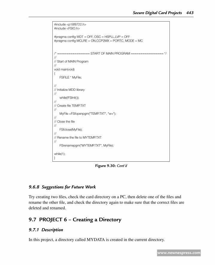
968 suggestions for Future Work
Try creating two files, check the card directory on a PC, then delete one of the files and rename the other file, and check the directory again to make sure that the correct files are deleted and renamed.
9.7 PrOJeCt 6 – Creating a directory
971 Description
In this project, a directory called MYDATA is created in the current directory.
#include <p18f8722.h>#include <FSIO.h>
#pragma config WDT = OFF, OSC = HSPLL,LVP = OFF#pragma config MCLRE = ON,CCP2MX = PORTC, MODE = MC
/* ================= START OF MAIN PROGRAM ================= *///// Start of MAIN Program//void main(void) FSFILE * MyFile;
//// Initialize MDD library// while(!FSInit( ));//// Create file TEMP.TXT// MyFile =FSfopenpgm("TEMP.TXT", "w+");//// Close the file// FSfclose(MyFile);//// Rename the file to MYTEMP.TXT// FSrenamepgm("MYTEMP.TXT", MyFile);
while(1);
Figure 9.30: Cont’d
secure Digital Card Projects 443
www.newnespress.com

972 Aim
The aim of this project is to show how a directory can be created using the MDD library functions.
973 Block Diagram
The block diagram of this project is as in Figure 9.16.
974 Circuit Diagram
The circuit diagram of this project is the same as in Figure 9.17.
975 Operation of the Project
The operation of the project is shown in Figure 9.31.
976 Program Code
The program code is shown in Figure 9.32.
977 Description of the Program Code
The program (DIR1.C) initializes the MDD library and calls the function FSmkdir to create a directory within the default working directory.
978 suggestions for Future Work
Create two directories called DATA1 and DATA2 in the current working directory. Then, create a directory called DATA1-1 inside the first directory. Check the card directory using a PC.
BEGIN Initialise the MDD library Create a directoryEND
Figure 9.31: Operation of the Project
444 Chapter 9
www.newnespress.com
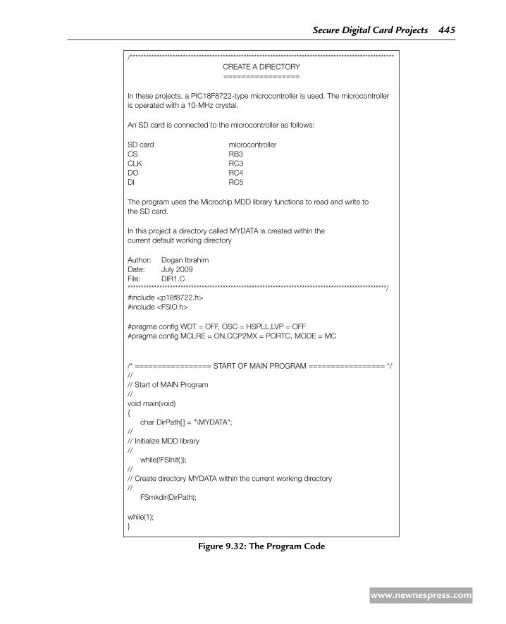
Figure 9.32: the Program Code
/****************************************************************************************************CREATE A DIRECTORY=================
In these projects, a PIC18F8722-type microcontroller is used. The microcontrolleris operated with a 10-MHz crystal.
An SD card is connected to the microcontroller as follows:
SD card microcontrollerCS RB3CLK RC3DO RC4DI RC5
The program uses the Microchip MDD library functions to read and write tothe SD card.
In this project a directory called MYDATA is created within thecurrent default working directory
Author: Dogan IbrahimDate: July 2009File: DIR1.C**************************************************************************************************/#include <p18f8722.h>#include <FSIO.h>
#pragma config WDT = OFF, OSC = HSPLL,LVP = OFF#pragma config MCLRE = ON,CCP2MX = PORTC, MODE = MC
/* ================= START OF MAIN PROGRAM ================= *///// Start of MAIN Program//void main(void) char DirPath[ ] = "\MYDATA";//// Initialize MDD library// while(!FSInit( ));//// Create directory MYDATA within the current working directory// FSmkdir(DirPath);
while(1);
secure Digital Card Projects 445
www.newnespress.com

9.8 PrOJeCt 7 – Create a directory and a File
981 Description
In this project, a directory called MYDATA is created in the current directory and then a file called RESULTS.DAT is created inside this directory. The following numbers are written inside this file: 24, 45, 22, 10, 28, 30.
982 Aim
The aim of this project is to show how a directory and a file inside this directory can be created using the MDD library functions.
983 Block Diagram
The block diagram of this project is as in Figure 9.16.
984 Circuit Diagram
The circuit diagram of this project is the same as in Figure 9.17.
985 Operation of the Project
The operation of the project is shown in Figure 9.33.
986 Program Code
The program code is shown in Figure 9.34.
987 Description of the Program Code
The program (DIR2.C) initializes the MDD library and calls the function FSmkdir to create a directory MYDATA within the default working directory. Then the function FSchdir is used to change the working directory to MYDATA. The file RESULTS.DAT is then created inside
Figure 9.33: Operation of the Project
BEGIN Initialise the MDD library Create a directory Create a file inside this directory Write numbers inside the file Close the fileEND
446 Chapter 9
www.newnespress.com

/*****************************************************************************************************CREATE A DIRECTORY AND A FILE==========================
In these projects, a PIC18F8722-type microcontroller is used. The microcontrolleris operated with a 10-MHz crystal.
An SD card is connected to the microcontroller as follows:
SD card microcontrollerCS RB3CLK RC3DO RC4DI RC5
The program uses the Microchip MDD library functions to read and write tothe SD card.
In this project a directory called MYDATA is created within the current defaultworking directory and then a file called RESULTS.DAT is created inside this directory. Some numbers are then written into this file
Author: Dogan IbrahimDate: July 2009File: DIR2.C*****************************************************************************************************/#include <p18f8722.h>#include <FSIO.h>
#pragma config WDT = OFF, OSC = HSPLL,LVP = OFF#pragma config MCLRE = ON,CCP2MX = PORTC, MODE = MC
/* ================ START OF MAIN PROGRAM ================== *///// Start of MAIN Program//void main(void) FSFILE * MyFile;
char DirPath[ ] = "\MYDATA"; char txt[ ] = "24, 45, 22,10, 28, 30";//// Initialize MDD library// while(!FSInit( ));//// Create directory MYDATA within the current working directory// FSmkdir(DirPath);
Figure 9.34: the Program Code
secure Digital Card Projects 447
www.newnespress.com

//// Change default working directory to MYDATA// FSchdir(DirPath);//// Create a file in this directory// MyFile = FSfopenpgm("RESULTS.DAT", "w+");//// Write numbers into this file// FSfwrite((void *)txt, 1, 17, MyFile);//// Close the file// FSfclose(MyFile);
while(1);
Figure 9.34: Cont’d
this directory and the required numbers are written to this file. The contents of the card can be verified using a PC to list the card directory.
988 suggestions for Future Work
Create a directory called MYTEXT inside the current default directory. Then, create two files inside this directory and write some text to both the files. Verify the card directory and contents of the files using a PC.
9.9 PrOJeCt 8 – File Copying
991 Description
In this project, the contents of a file are copied to another file. The source file called SRC.TXT is loaded with some text using a PC. The contents of this file are then copied to a file called DST.TXT. The success of the copy operation is verified by reading the destination file on a PC.
992 Aim
The aim of this project is to show how multiple files can be handled using the MDD library. In addition, the steps to read and write to a card are described in this project.
448 Chapter 9
www.newnespress.com

993 Block Diagram
The block diagram of this project is as in Figure 9.16.
994 Circuit Diagram
The circuit diagram of this project is the same as in Figure 9.17.
995 Operation of the Project
The operation of the project is shown in Figure 9.35.
996 Program Code
The program code (COPY.C) is shown in Figure 9.36.
997 Description of the Program Code
After initializing the MDD library, file SRC.TXT is opened in read mode and file DST.TXT is created as a new file. Then a while loop is formed and the statements inside this loop are executed until the end of the source file is reached. Inside this loop, 10 items of 1 byte each are read (other sizes could also be used). Variable ReadCnt actually stores the number of bytes read from SRC.TXT. The data is then written to file DST.TXT. Both the source and the destination files are closed at the end of the copy operation.
998 suggestions for Future Work
Modify the program given in Figure 9.36 to copy a file using different numbers of items and different lengths for each item.
Figure 9.35: Operation of the Project
BEGIN Initialise the MDD library Open source file Open destination file WHILE not end of source file Read from source file Write to destination file WEND Close source file Close destination fileEND
secure Digital Card Projects 449
www.newnespress.com

/******************************************************************************************************FILE COPY========
In these projects, a PIC18F8722-type microcontroller is used. The microcontrolleris operated with a 10-MHz crystal.
An SD card is connected to the microcontroller as follows:
SD card microcontrollerCS RB3CLK RC3DO RC4DI RC5
The program uses the Microchip MDD library functions to read and write tothe SD card.
In this project a file called SRC.TXT is copied to another filecalled DST.TXT. It is assumed that SRC.TXT had some text data init before the copy operation.
Author: Dogan IbrahimDate: July 2009File: COPY.C*****************************************************************************************************/#include <p18f8722.h>#include <FSIO.h>
#pragma config WDT = OFF, OSC = HSPLL,LVP = OFF#pragma config MCLRE = ON,CCP2MX = PORTC, MODE = MC
/* ================== START OF MAIN PROGRAM ================== *///// Start of MAIN Program//void main(void) FSFILE *MySrcFile, *MyDstFile; char bufr[10]; char ReadCnt;//// Initialize MDD library// while(!FSInit( ));//// Open the source file// MySrcFile = FSfopenpgm("SRC.TXT", "r");
Figure 9.36: the Program Code
450 Chapter 9
www.newnespress.com

//// Create the destination file// MyDstFile = FSfopenpgm("DST.TXT", "w+");//// Read from SRC.TXT and write to DST.TXT until the end-of-file// while(FSfeof(MySrcFile) == 0) ReadCnt = FSfread((void *)bufr,1, 10, MySrcFile); FSfwrite((void *)bufr, 1, ReadCnt, MyDstFile); //// Close the files// FSfclose(MySrcFile); FSfclose(MyDstFile);
while(1);
9.10 PrOJeCt 9 – displaying File on a PC
9101 Description
In this project, the contents of a file are displayed on a PC connected to the microcontroller. Before starting the project, a file called MYTEST.TXT is created on the SD card using a PC and this file is loaded with some text. The card is then connected to the microcontroller, the file is opened and its contents are displayed on the PC screen. The message “Displaying the file…” is sent to the PC before displaying contents of the file.
9102 Aim
The aim of this project is to show how the serial port of the microcontroller can be connected to a PC and how the contents of a file can be displayed on the PC screen using the MDD library functions.
9103 Block Diagram
The block diagram of this project is as in Figure 9.37.
Figure 9.36: Cont’d
secure Digital Card Projects 451
www.newnespress.com
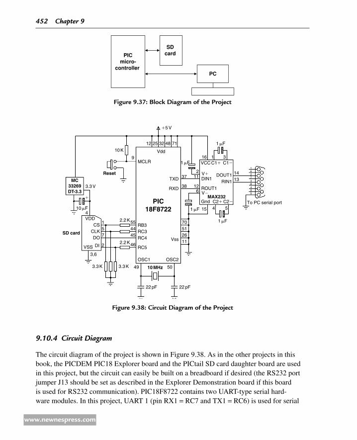
Figure 9.37: Block diagram of the Project
PC
PICmicro-
controller
SD card
Figure 9.38: Circuit diagram of the Project
MC33269DT-3.3
SD card
3.3 V
Reset
MCLR
Vdd
VDD4
VSS
DO
CS
DI
CLK
TXD
RXD
10 F
10 K
9
157
2
554445
15 54
211
12
37
16 1 31 F
1 F
1 F
1 F
VCC C1
V
V
DIN1
ROUT1
To PC serial port
DOUT1RIN1
Gnd C2
5 V
MAX232PIC
18F8722C2
C1
38
14162738495
13
6
70
12 25 32 48 71
512611
46
49
22 pF 22 pF
10 MHz 50
3,6
2.2 KRB3RC3RC4
RC5
OSC1 OSC2
Vss2.2 K
3.3 K3.3 K
9104 Circuit Diagram
The circuit diagram of the project is shown in Figure 9.38. As in the other projects in this book, the PICDEM PIC18 Explorer board and the PICtail SD card daughter board are used in this project, but the circuit can easily be built on a breadboard if desired (the RS232 port jumper J13 should be set as described in the Explorer Demonstration board if this board is used for RS232 communication). PIC18F8722 contains two UART-type serial hard-ware modules. In this project, UART 1 (pin RX1 = RC7 and TX1 = RC6) is used for serial
452 Chapter 9
www.newnespress.com

communication and is connected to a MAX232-type level converter chip. This chip converts the 0 to +5-V TTL level output voltage of the microcontroller to ±12-V RS232 levels and also the ±12 V RS232 levels to 0 to +5 V required for the microcontroller inputs. The MAX232 is connected to the serial port of a PC via a 9-pin D-type connector.
There are two types of RS232 connector: 9-pin and 25-pin. The required pins in each type are as follows:
Figure 9.39: Operation of the Project
BEGIN Initialize USART module Initialize the MDD library Open file on SD card WHILE not end of source file Read from source file Send to USART WEND Close file Close USARTEND
Pins Signals
9-pin
2 Transmit (TX)
3 Receive (RX)
5 Ground (GND)
25-pin
2 Transmit (TX)
3 Receive (RX)
7 Ground (GND)
9105 Operation of the Project
The operation of the project is shown in Figure 9.39.
9106 The Program Code
The program code (RS232.C) is shown in Figure 9.40.
9107 Description of the Program Code
At the beginning of the program, the USART module is initialized by calling the C18 library function Open1USART (since there are two USART modules on the PIC18F8722 microcontroller, we have to specify which module we shall be using). Serial port interrupts are disabled, USART is set to asynchronous mode, and the baud-rate clock is set to low
secure Digital Card Projects 453
www.newnespress.com

Figure 9.40: the Program Code
/******************************************************************************************************** SEND FILE CONTENTS TO THE PC ==========================
In these projects, a PIC18F8722-type microcontroller is used. The microcontrolleris operated with a 10-MHz crystal.
An SD card is connected to the microcontroller as follows:
SD card microcontrollerCS RB3CLK RC3DO RC4DI RC5
The program uses the Microchip MDD library functions to read and write tothe SD card.
In this project the microcontroller is connected to a PC via a MAX232-typelevel converter chip. USART 1 hardware module of the microcontroller is usedfor serial communication. The pin configuration of the RS232 connector is asfollows:
Pin 2 TX Pin 3 RX Pin 3 GND
The communication is established using the C18 USART library functions. The USART is configured as follows:
4800 Baud 8 data bits No parity 1 stop bit
In this project a text file called MYTEST.TXT is opened on the SD card and the contents of this file are displayed on the PC.
Author: Dogan IbrahimDate: August 2009File: RS232.C********************************************************************************************************/#include <p18f8722.h>#include <usart.h>#include <FSIO.h>
#pragma config WDT = OFF, OSC = HSPLL, LVP = OFF#pragma config MCLRE = ON, CCP2MX = PORTC, MODE = MC
454 Chapter 9
www.newnespress.com

/* ==================START OF MAIN PROGRAM ================= *///// Start of MAIN Program//void main(void) FSFILE *MySrcFile; char bufr[1];
//// Initialize the USART// Open1USART( USART_TX_INT_OFF & USART_RX_INT_OFF & USART_ASYNCH_MODE & USART_EIGHT_BIT & USART_CONT_RX & USART_BRGH_LOW, 129);//// Send a message to the PC// while(Busy1USART( )); putrs1USART(" Displaying the file...\n\r");//// Initialize MDD library// while(!FSInit( ));//// Open the source file// MySrcFile = FSfopenpgm("MYTEST.TXT", "r");//// Read from the file and send to the PC until the end-of-file// while(FSfeof(MySrcFile) == 0) FSfread((void *)bufr,1, 1, MySrcFile); while(Busy1USART( )); putc1USART(bufr[0]); //// Close the file// FSfclose(MySrcFile);//// Close USART// Close1USART( );
while(1);
Figure 9.40: Cont’d
secure Digital Card Projects 455
www.newnespress.com

speed. In this project, the serial communication baud rate is set to 4800. The last argument of openUSART (spbrg) sets the baud rate according to the formula:
Baud rate = Fosc/(64 × (spbrg + 1)),
where Fosc is the microcontroller operating clock frequency. Here, the value of spbrg is calculated as
spbrg = Fosc/(64 × baud rate) − 1
giving
spbrg = 40 × 106/(64 × 4800) − 1 = 129
Then the message “Displaying the file…,” followed by the characters carriage-return and line feed are sent to the PC. File MYTEST.TXT is then opened in read mode on the SD card. A while loop is formed that executes as long as the end of file is not detected. Inside this loop, a byte is read from the file using the function FSfread and this byte is sent to the USART by calling the function putc1USART. Note that we should make sure that the USART is ready to receive a character before we send the next character. After all the data in the file is sent, the file is closed and the USART is disabled by closing it.
The operation of the program can be tested using a serial communications program on the PC, such as the HyperTerminal. The steps in using this program are given below:
Start the HyperTerminal program by selecting it from Start -> Programs -> •Accessories -> Communications -> HyperTerminal
Enter a name for the connection (e.g., TEST) and click OK (see Figure 9.41) •
Figure 9.41: Create a New Serial Connection
456 Chapter 9
www.newnespress.com

Figure 9.42: Select the Serial Port Number
Select the serial port the microcontroller is connected to. In this example, COM2 is used, •as shown in Figure 9.42. (If you are not sure which serial ports are available in your PC, check the Device Manager in Control Panel. Most modern PCs do not have any serial ports and you may have to use a serial to USB connector device to provide serial ports to your PC.) Click OK.
Select the serial port parameters as (see Figure 9.43) •
Bits per second: 4800
Data bits: 8
Parity: None
Stop bits: 1
Flow control: None
Click Apply and OK.
Insert the SD card into its holder and make sure that there is a file called MYTEST.TXT •on the card.
Press the Reset button. The contents of the file should be displayed on the PC (see the •example in Figure 9.44).
9108 suggestions for Future Work
Write a program to read a file name from the PC and then open this file on the SD card and display its contents on the PC screen.
secure Digital Card Projects 457
www.newnespress.com

Figure 9.43: Select the Serial Port Parameters
Figure 9.44: example PC display
9.11 PrOJeCt 10 – reading a Filename from the PC and displaying the File
9111 Description
In this project, the name of a file is received from the PC and then contents of this file are displayed on the PC. Before starting the project, it is assumed that a file called MYTEST.TXT exists on the SD card. The following message is displayed on the PC screen by the
458 Chapter 9
www.newnespress.com

microcontroller (the filename string is terminated when the Enter key is pressed on the PC keyboard):
Enter the Filename:
9112 Aim
The aim of this project is to show how a string of data can be received from a PC and how a file can be opened on the SD card and its contents displayed on the PC screen.
9113 Block Diagram
The block diagram of this project is as in Figure 9.37.
9114 Circuit Diagram
The circuit diagram of this project is as in Figure 9.38.
9115 Operation of the Project
The operation of the project is shown in Figure 9.45.
9116 Program Code
The program code (RS232-2.C) is shown in Figure 9.46.
9117 Description of the Program Code
The USART module is initialized at the beginning of the program (as in the earlier project) by calling to C18 library function Open1USART (since there are two USART modules on the PIC18F8722 microcontroller, we have to specify which module we shall be using).
Figure 9.45: Operation of the Project
BEGIN Initialize USART module Initialize the MDD library Display a heading message Read the filename Open the file on SD card WHILE not end of source file Read from the file Send to USART WEND Close the file Close USARTEND
secure Digital Card Projects 459
www.newnespress.com

/********************************************************************************************************** READ FILENAME AND SEND FILE CONTENTS TO THE PC ===========================================
In these projects, a PIC18F8722-type microcontroller is used. The microcontrolleris operated with a 10-MHz crystal.
An SD card is connected to the microcontroller as follows:
SD card microcontrollerCS RB3CLK RC3DO RC4DI RC5
The program uses the Microchip MDD library functions to read and write tothe SD card.
In this project the microcontroller is connected to a PC viaa MAX232-type level converter chip. USART 1 hardware moduleof the microcontroller is used for serial communication. Thepin configuration of the RS232 connector is as follows:
Pin 2 TX Pin 3 RX Pin 3 GND
The communication is established using the C18 USART libraryfunctions. The USART is configured as follows:
4800 Baud 8 data bits No parity 1 stop bit
In this project the filename is read from the PC keyboard and the content ofthe file is displayed on the PC screen (it is assumed that the requested file existson the SD card).
Figure 9.46: the Program Code
Serial port interrupts are disabled, USART is set to asynchronous mode, the baud-rate clock is set to low speed, and the baud rate is set to 4800. The message “Enter the Filename:” is displayed on the PC screen and the user is requested to enter the name of the file. The filename is stored in a character array called FileName. This array is terminated with a NULL character as the function FSfopen requires the name to be a NULL-terminated string. The required text file is then opened on the SD card and its contents are displayed on the PC screen as in the earlier project.
Figure 9.47 shows a typical output from the project.
460 Chapter 9
www.newnespress.com
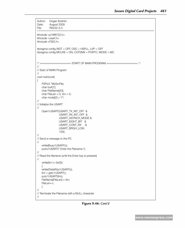
Author: Dogan IbrahimDate: August 2009File: RS232-2.C*************************************************************************************************************************#include <p18f8722.h>#include <usart.h>#include <FSIO.h>
#pragma config WDT = OFF, OSC = HSPLL, LVP = OFF#pragma config MCLRE = ON, CCP2MX = PORTC, MODE = MC
/* =================== START OF MAIN PROGRAM =================== *///// Start of MAIN Program//void main(void) FSFILE *MySrcFile; char bufr[1]; char FileName[20]; char FileLen = 0, itm = 0; char mode[2] = "r";//// Initialize the USART// Open1USART(USART_TX_INT_OFF &
USART_RX_INT_OFF &USART_ASYNCH_MODE &USART_EIGHT_BIT &USART_CONT_RX &USART_BRGH_LOW, 129);
//// Send a message to the PC// while(Busy1USART( )); putrs1USART(" Enter the Filename:");//// Read the filename (until the Enter key is pressed)// while(itm != 0x0D) while(!DataRdy1USART( )); itm = getc1USART( ); putc1USART(itm); FileName[FileLen] = itm; FileLen++; //// Terminate the Filename with a NULL character//
Figure 9.46: Cont’d
secure Digital Card Projects 461
www.newnespress.com

FileLen--; FileName[FileLen] = '\0';//// Insert a new line// putrs1USART("\n\r"); //// Initialize MDD library// while(!FSInit( ));//// Open the file// MySrcFile = FSfopen(FileName, mode);//// Read from the file and send to the PC until the end-of-file// while(FSfeof(MySrcFile) == 0) FSfread((void *)bufr,1, 1, MySrcFile); while(Busy1USART( )); putc1USART(bufr[0]); //// Close the file// FSfclose(MySrcFile);//// Close USART// Close1USART( );
while(1);
Figure 9.46: Cont’d
Figure 9.47: example PC display
462 Chapter 9
www.newnespress.com

9118 suggestions for Future Work
Store several files on the SD card with the extension “.DAT.” Write a program to read a file name from the keyboard without the file extension. Append the extension “.DAT” to the file name and display the contents of the file on the PC screen.
9.12 PrOJeCt 11 – Looking for a File
9121 Description
In this project, the current directory is searched for a given filename with any attribute value. The name of the file to be searched is entered from the PC keyboard as in Project 10. If the file is not found, the message NOT FOUND is displayed; if the file is found, the size of the file is displayed in bytes on the PC screen.
9122 Aim
The aim of this project is to show how a file can be searched in the current directory using the MDD library functions.
9123 Block Diagram
The block diagram of this project is as in Figure 9.37.
9124 Circuit Diagram
The circuit diagram of this project is as in Figure 9.38.
9125 Operation of the Project
The operation of the project is shown in Figure 9.48.
BEGIN Initialize USART module Initialize the MDD library Read the filename Search for the file in current directory IF file not found Display NOT FOUND ELSE Display size of the file ENDIF Close USARTEND
Figure 9.48: Operation of the Project
secure Digital Card Projects 463
www.newnespress.com
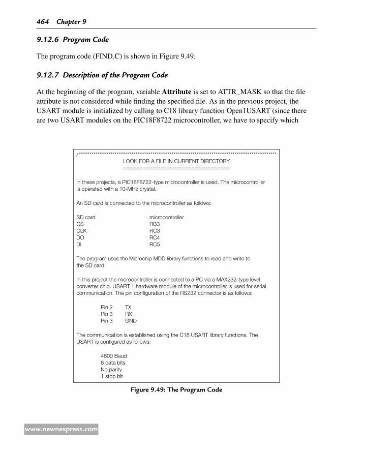
9126 Program Code
The program code (FIND.C) is shown in Figure 9.49.
9127 Description of the Program Code
At the beginning of the program, variable Attribute is set to ATTR_MASK so that the file attribute is not considered while finding the specified file. As in the previous project, the USART module is initialized by calling to C18 library function Open1USART (since there are two USART modules on the PIC18F8722 microcontroller, we have to specify which
/******************************************************************************************************** LOOK FOR A FILE IN CURRENT DIRECTORY =================================
In these projects, a PIC18F8722-type microcontroller is used. The microcontroller is operated with a 10-MHz crystal.
An SD card is connected to the microcontroller as follows:
SD card microcontrollerCS RB3CLK RC3DO RC4DI RC5
The program uses the Microchip MDD library functions to read and write to the SD card.
In this project the microcontroller is connected to a PC via a MAX232-type level converter chip. USART 1 hardware module of the microcontroller is used for serial communication. The pin configuration of the RS232 connector is as follows:
Pin 2 TX Pin 3 RX Pin 3 GND
The communication is established using the C18 USART library functions. The USART is configured as follows:
4800 Baud 8 data bits No parity 1 stop bit
Figure 9.49: the Program Code
464 Chapter 9
www.newnespress.com

In this project a given file is searched in the current default directory and the message NOT FOUND is displayed if the file is not found; otherwise, the size of the file is displayed on the PC screen.
Author: Dogan IbrahimDate: August 2009File: FIND.C*******************************************************************************************************/#include <p18f8722.h>#include <usart.h>#include <stdlib.h>#include <FSIO.h>
#pragma config WDT = OFF, OSC = HSPLL,LVP = OFF#pragma config MCLRE = ON,CCP2MX = PORTC, MODE = MC
/* ================= START OF MAIN PROGRAM ================== *///// Start of MAIN Program//void main(void) FSFILE *MySrcFile; SearchRec File; char bufr[1]; char FileName[20]; char FileLen = 0, itm = 0; unsigned char Attribute = ATTR_MASK; unsigned long FileSize; unsigned char FileSizeStr[10];//// Initialize the USART// Open1USART(USART_TX_INT_OFF &
USART_RX_INT_OFF &USART_ASYNCH_MODE &USART_EIGHT_BIT &USART_CONT_RX &USART_BRGH_LOW, 129);
//// Send a message to the PC// while(Busy1USART( )); putrs1USART(" Enter the Filename:");//// Read the filename (until the Enter key is pressed)//
Figure 9.49: Cont’d
secure Digital Card Projects 465
www.newnespress.com

while(itm != 0x0D) while(!DataRdy1USART( )); itm = getc1USART( ); putc1USART(itm); FileName[FileLen] = itm; FileLen++; //// Terminate the Filename with a NULL character//
FileLen−−; FileName[FileLen] = '\0';//// Insert a new line// putrs1USART("\n\r"); //// Initialize MDD library// while(!FSInit( ));//// Look for the file// if(FindFirst(FileName, Attribute, &File) != 0) putrs1USART("NOT FOUND"); else FileSize = File.filesize; ltoa(FileSize, ( void*)FileSizeStr); puts1USART((void *)FileSizeStr); //// Close USART// Close1USART( );
while(1);
Figure 9.49: Cont’d
module we shall be using). Serial port interrupts are disabled, USART is set to asynchronous mode, the baud-rate clock is set to low speed, and the baud rate is set to 4800. The message “Enter the Filename:” is displayed on the PC screen, and the user is requested to enter the name of the file. The filename is stored in a character array called FileName and is terminated with a NULL character.
The MDD library function FindFirst is called to search for the specified file in the cur-rent default directory. If the file is not found, the function returns a nonzero value and the message “NOT FOUND” is displayed on the PC screen. If the file is found, its size is
466 Chapter 9
www.newnespress.com

extracted from the filesize member of structure SearchRec. The file size is a long variable; it is converted into a string using the C18 library function ltoa and is stored in character array FileSizeStr. USART function puts1USART is then called to display the file size (in bytes).
Figure 9.50 shows a typical output from the project where the size of the file was 112 bytes.
9128 suggestions for Future Work
Write a program to look for a file on the SD card, and if the file is found, display the creation date of the file; otherwise, display a message “NOT FOUND” on the PC screen.
9.13 PrOJeCt 12 – Looking for a Number of Files with a Given File extension
9131 Description
In this project, a file extension is given and then all the files in the current directory with the given extension name are found and listed on the PC screen. If no files are found, the message “NO SUCH FILES” is displayed. For example, if the file extension is specified as
*.TXT,
then all the files having extensions “TXT” will be searched for in the current directory.
9132 Aim
The aim of this project is to show how multiple files can be searched in the current directory using the MDD library functions.
Figure 9.50: example PC display
secure Digital Card Projects 467
www.newnespress.com

9133 Block Diagram
The block diagram of this project is as in Figure 9.37.
9134 Circuit Diagram
The circuit diagram of this project is as in Figure 9.38.
9135 Operation of the Project
The operation of the project is shown in Figure 9.51.
9136 Program Code
The program code (FINDEXT.C) is shown in Figure 9.52.
9137 Description of the Program Code
At the beginning of the program, variable Attribute is set to ATTR_MASK so that the file attribute is not considered while finding the specified files. As in the previous project, the USART module is initialized by calling to C18 library function Open1USART (since there are two USART modules on the PIC18F8722 microcontroller, we have to specify which module we shall be using). Serial port interrupts are disabled, USART is set to asynchronous mode, the baud-rate clock is set to low speed, and the baud rate is set to 4800. The message “Enter the File extension:” is displayed on the PC screen and the user is requested to enter the file extension name. The file extension is stored in a character array called FileName and is terminated with a NULL character.
The MDD library function FindFirst is called to search for the specified file in the current default directory. If the file is not found, the function returns a nonzero value and the message “NO SUCH FILES” is displayed on the PC screen. If a file is found matching the specified
BEGIN Initialize USART module Initialize the MDD library Read the file extension Search for all files with the given extension IF file not found Display NO SUCH FILES ELSE Display names of all found files ENDIF Close USARTEND
Figure 9.51: Operation of the Project
468 Chapter 9
www.newnespress.com
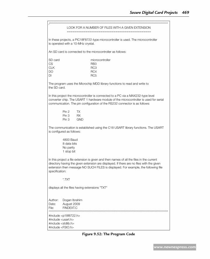
/************************************************************************************************************ LOOK FOR A NUMBER OF FILES WITH A GIVEN EXTENSION =============================================
In these projects, a PIC18F8722-type microcontroller is used. The microcontrolleris operated with a 10-MHz crystal.
An SD card is connected to the microcontroller as follows:
SD card microcontrollerCS RB3CLK RC3DO RC4DI RC5
The program uses the Microchip MDD library functions to read and write tothe SD card.
In this project the microcontroller is connected to a PC via a MAX232-type level converter chip. The USART 1 hardware module of the microcontroller is used for serial communication. The pin configuration of the RS232 connector is as follows:
Pin 2 TX Pin 3 RX Pin 3 GND
The communication is established using the C18 USART library functions. The USART is configured as follows:
4800 Baud 8 data bits No parity 1 stop bit
In this project a file extension is given and then names of all the files in the current directory having the given extension are displayed. If there are no files with the given extension then message NO SUCH FILES is displayed. For example, the following file specification:
*.TXT
displays all the files having extensions "TXT"
Author: Dogan IbrahimDate: August 2009File: FINDEXT.C*************************************************************************************************************#include <p18f8722.h>#include <usart.h>#include <stdlib.h>#include <FSIO.h>
Figure 9.52: the Program Code
secure Digital Card Projects 469
www.newnespress.com

#pragma config WDT = OFF, OSC = HSPLL,LVP = OFF#pragma config MCLRE = ON,CCP2MX = PORTC, MODE = MC
/* =============== START OF MAIN PROGRAM ================ *///// Start of MAIN Program//void main(void) FSFILE *MySrcFile; SearchRec File; char bufr[1]; char FileName[12]; char FileLen = 0, itm = 0; unsigned char Attribute = ATTR_MASK; char Flag = 0;//// Initialize the USART// Open1USART(USART_TX_INT_OFF & USART_RX_INT_OFF & USART_ASYNCH_MODE & USART_EIGHT_BIT & USART_CONT_RX & USART_BRGH_LOW, 129);//// Send a message to the PC// while(Busy1USART( )); putrs1USART(" Enter the File extension: ");//// Read the filename (until the Enter key is pressed)// while(itm != 0x0D) while(!DataRdy1USART( )); itm = getc1USART( ); putc1USART(itm); FileName[FileLen] = itm; FileLen++; //// Terminate the Filename with a NULL character// FileLen--; FileName[FileLen] = '\0';//// Insert a new line// putrs1USART("\n\r");
Figure 9.52: Cont’d
470 Chapter 9
www.newnespress.com

//// Initialize MDD library// while(!FSInit( ));//// Look for the files with given extension// if(FindFirst(FileName, Attribute, &File) != 0) putrs1USART("NO SUCH FILES"); else puts1USART(File.filename); putrs1USART("\n\r"); while(Flag == 0) if(FindNext(&File) != 0) Flag = 1; else puts1USART(File.filename); putrs1USART("\n\r"); //// Close USART// Close1USART( );
while(1);
Figure 9.52: Cont’d
extension name, then the full name of this file is extracted from the filename member of structure SearchRec and the filename is displayed on the PC screen using USART function puts1USART. The MDD function FindNext is then called in a while loop to check if there are any more files with the specified extension name. The return of function FindNext is zero if another file is found, and the name of the found file is displayed, followed by a new-line character. When there are no more files matching the specified extension name, then function FindNext returns a nonzero value and the variable Flag is set to 1 to terminate the while loop.
Figure 9.53 shows a typical output from the project. In this example, there are six files on the SD card with the following names:
TEST1.TXT
TEST2.TXT
secure Digital Card Projects 471
www.newnespress.com

TEST3.TXT
TEST4.TXT
TEST5.DAT
TEST6.DAT
Only the files with extensions “TXT” are displayed.
Note that the program given in this project can be used to look for other types of files. Some examples are given below:
*.* All files in the current directory
*.ext Files with extension “ext”
File.* Files with name “File”
* Any directory
9138 suggestions for Future Work
Write a program to look for a file in the current directory and in all the subdirectories of the SD card.
9.14 PrOJeCt 13 – displaying the attributes of a File
9141 Description
In this project, a file name is read from the PC keyboard and then the specified file is searched on the SD card and the attributes of the file are displayed on the PC screen. If the file does not exist, then the message “NO SUCH FILE” is displayed.
Figure 9.53: example PC display
472 Chapter 9
www.newnespress.com

9142 Aim
The aim of this project is to show how the attributes of a given file can be determined.
9143 Block Diagram
The block diagram of this project is as in Figure 9.37.
9144 Circuit Diagram
The circuit diagram of this project is as in Figure 9.38.
9145 Operation of the Project
The operation of the project is shown in Figure 9.54.
9146 Program Code
The program code (ATTR.C) is shown in Figure 9.55.
9147 Description of the Program Code
At the beginning of the program, the variable Attribute is set to ATTR_MASK so that the file attribute is not considered while finding the specified file. As in the previous project, the USART module is initialized by calling to C18 library function Open1USART (since there are two USART modules on the PIC18F8722 microcontroller, we have to specify which module we shall be using). Serial port interrupts are disabled, USART is set to asynchronous mode, the baud-rate clock is set to low speed, and the baud rate is set to 4800. The message “Enter the Filename:” is displayed on the PC screen and the user is requested to enter the file name. The file name is stored in a character array called FileName and is terminated with a NULL character.
BEGIN Initialize USART module Initialize the MDD library Read the filename Search for the file IF file not found Display NO SUCH FILE ELSE Display attributes of the file ENDIF Close USARTEND
Figure 9.54: Operation of the Project
secure Digital Card Projects 473
www.newnespress.com

/*********************************************************************************************************************DISPLAY ATTRIBUTES OF A FILE========================
In these projects, a PIC18F8722-type microcontroller is used. The microcontroller is operated with a 10-MHz crystal.
An SD card is connected to the microcontroller as follows:
SD card microcontrollerCS RB3CLK RC3DO RC4DI RC5
The program uses the Microchip MDD library functions to read and write tothe SD card.
In this project the microcontroller is connected to a PC via a MAX232-type level converter chip. The USART 1 hardware module of the microcontroller is used for serial communication. The pin configuration of the RS232 connector is as follows:
Pin 2 TX Pin 3 RX Pin 3 GND
The communication is established using the C18 USART library functions. TheUSART is configured as follows:
4800 Baud 8 data bits No parity 1 stop bit
In this project a file name is read from the PC keyboard and then the attributes of this file are found and displayed on the PC screen.
Author: Dogan IbrahimDate: August 2009File: ATTR.C*********************************************************************************************************************/#include <p18f8722.h>#include <usart.h>#include <stdlib.h>#include <FSIO.h>
#pragma config WDT = OFF, OSC = HSPLL,LVP = OFF#pragma config MCLRE = ON,CCP2MX = PORTC, MODE = MC
Figure 9.55: the Program Code
474 Chapter 9
www.newnespress.com

/* ================ START OF MAIN PROGRAM ================ *///// Start of MAIN Program//void main(void) SearchRec File; char bufr[1]; char FileName[12]; char FileLen = 0, itm = 0; unsigned char Attribute = ATTR_MASK; unsigned char Attributes;//// Initialize the USART// Open1USART(USART_TX_INT_OFF & USART_RX_INT_OFF & USART_ASYNCH_MODE & USART_EIGHT_BIT & USART_CONT_RX & USART_BRGH_LOW, 129);//// Send a message to the PC// while(Busy1USART( )); putrs1USART(" Enter the Filename: ");//// Read the filename (until the Enter key is pressed)// while(itm != 0x0D) while(!DataRdy1USART( )); itm = getc1USART( ); putc1USART(itm); FileName[FileLen] = itm; FileLen++; //// Terminate the Filename with a NULL character// FileLen− −; FileName[FileLen] = '\0';//// Insert a new line// putrs1USART("\n\r"); //// Initialize MDD library
Figure 9.55: Cont’d
secure Digital Card Projects 475
www.newnespress.com
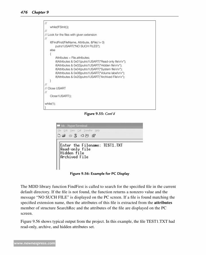
// while(!FSInit( ));//// Look for the files with given extension// if(FindFirst(FileName, Attribute, &File) != 0) putrs1USART("NO SUCH FILES"); else Attributes = File.attributes; if(Attributes & 0x01)putrs1USART("Read-only file\n\r"); if(Attributes & 0x02)putrs1USART("Hidden file\n\r"); if(Attributes & 0x04)putrs1USART("System file\n\r"); if(Attributes & 0x08)putrs1USART("Volume label\n\r"); if(Attributes & 0x20)putrs1USART("Archived File\n\r"); //// Close USART// Close1USART( );
while(1);
Figure 9.55: Cont’d
Figure 9.56: example for PC display
The MDD library function FindFirst is called to search for the specified file in the current default directory. If the file is not found, the function returns a nonzero value and the message “NO SUCH FILE” is displayed on the PC screen. If a file is found matching the specified extension name, then the attributes of this file is extracted from the attributes member of structure SearchRec and the attributes of the file are displayed on the PC screen.
Figure 9.56 shows typical output from the project. In this example, the file TEST1.TXT had read-only, archive, and hidden attributes set.
476 Chapter 9
www.newnespress.com

9148 suggestions for Future Work
Write a program to display a list of all the files in the current default working directory with their sizes and attributes.
9.15 PrOJeCt 14 – Sd Card File handling
9151 Description
In this project, a program is developed to handle a number of SD card operations. The following operations are performed:
CD Change directory
DEL Delete a file
DIR Directory listing
FORM Format SD card
HELP Help on these commands
MD Create a directory
RD Delete a directory
REN Rename a file
TYPE Display the contents of a file
COPY Copy a file
The command mode is identified by character “$” where any of the above commands can be entered. After entering a command, the user should press the Enter key and then enter the appropriate command option. The following command options are available for each command:
CDEnter directory name:
DELEnter filename:
DIR
FORMEnter volume name:
HELP
MdEnter directory name:
secure Digital Card Projects 477
www.newnespress.com

RdEnter directory name:
RENSource filename:Destination filename:
TYPEEnter filename:
COPYSource filename:Destination filename:
9152 Aim
The aim of this project is to show how several file-handling operations can be performed in a program.
9153 Block Diagram
The block diagram of this project is as in Figure 9.37.
9154 Circuit Diagram
The circuit diagram of this project is as in Figure 9.38.
9155 Operation of the Project
The operation of the project is shown in Figure 9.57.
9156 Program Code
The program code (FILES.C) is shown in Figure 9.58.
9157 Description of the Program Code
The following functions are used in the program:
Read_Filename: This function reads the filename, directory name, or the volume name from the keyboard. The argument specifies the text string to be displayed before accepting the user input. The function is terminated when the Enter key is pressed and a NULL character is added to the end of the name.
478 Chapter 9
www.newnespress.com
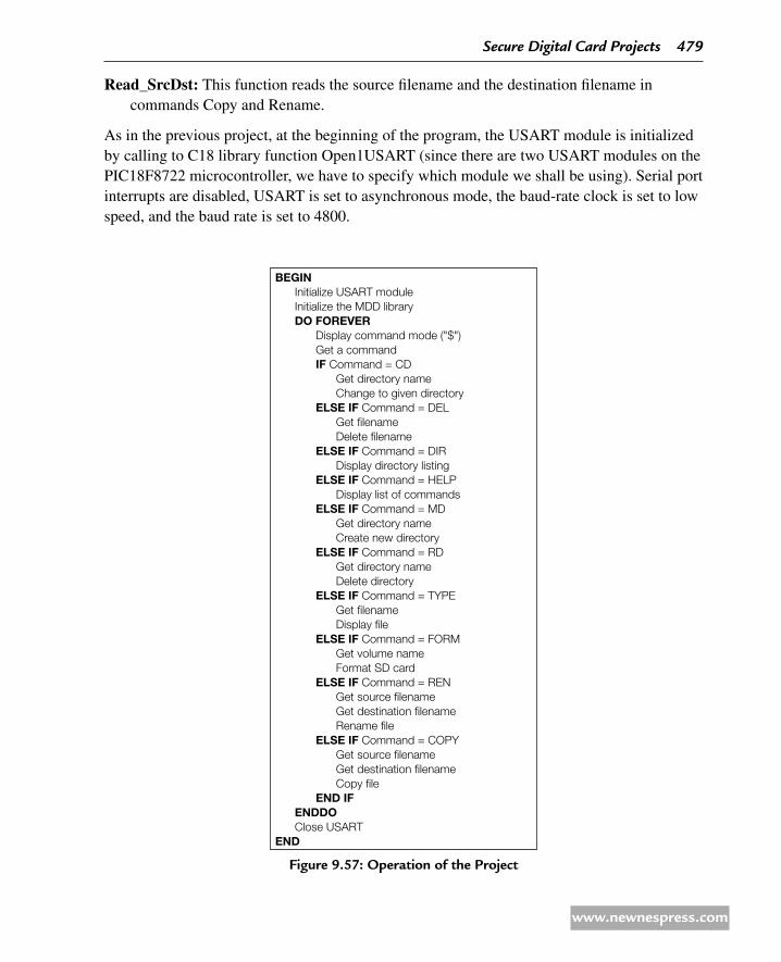
BEGIN Initialize USART module Initialize the MDD library DO FOREVER Display command mode ("$") Get a command IF Command = CD Get directory name Change to given directory ELSE IF Command = DEL Get filename Delete filename ELSE IF Command = DIR Display directory listing ELSE IF Command = HELP Display list of commands ELSE IF Command = MD Get directory name Create new directory ELSE IF Command = RD Get directory name Delete directory ELSE IF Command = TYPE Get filename Display file ELSE IF Command = FORM Get volume name Format SD card ELSE IF Command = REN Get source filename Get destination filename Rename file ELSE IF Command = COPY Get source filename Get destination filename Copy file END IF ENDDO Close USARTEND
Figure 9.57: Operation of the Project
Read_SrcDst: This function reads the source filename and the destination filename in commands Copy and Rename.
As in the previous project, at the beginning of the program, the USART module is initialized by calling to C18 library function Open1USART (since there are two USART modules on the PIC18F8722 microcontroller, we have to specify which module we shall be using). Serial port interrupts are disabled, USART is set to asynchronous mode, the baud-rate clock is set to low speed, and the baud rate is set to 4800.
secure Digital Card Projects 479
www.newnespress.com

/*************************************************************************************************SD CARD FILE HANDLING COMMANDS=============================
In these projects, a PIC18F8722-type microcontroller is used. The microcontrolleris operated with a 10-MHz crystal.
An SD card is connected to the microcontroller as follows:
SD card microcontrollerCS RB3CLK RC3DO RC4DI RC5
The program uses the Microchip MDD library functions to read and write to the SD card.
In this project the microcontroller is connected to a PC via a MAX232-type level converter chip. The USART 1 hardware module of the microcontroller is used for serial communication. The pin configuration of the RS232 connector is as follows:
Pin 2 TX Pin 3 RX Pin 3 GND
The communication is established using the C18 USART library functions. The USART is configured as follows:
4800 Baud 8 data bits No parity 1 stop bit
In this project various commands are provided for handling file operations on an SD card. The following commands are provided:
CD change directory DEL delete a file DIR directory listing FORM format SD card HELP help on these commands MD create a directory RD delete directory REN rename a file TYPE display contents of a file COPY copy a file
The command mode is identified with a $ character and the command should be entered after the command mode. The following command tails are available:
CD Enter Directory name:
Figure 9.58: the Program Code
480 Chapter 9
www.newnespress.com
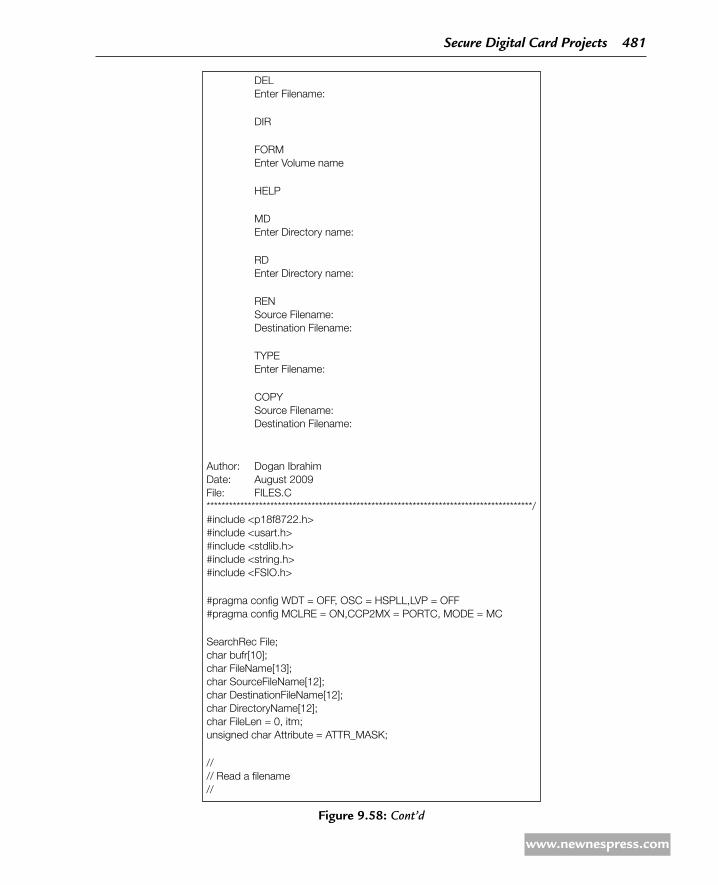
DEL Enter Filename:
DIR
FORM Enter Volume name
HELP
MD Enter Directory name:
RD Enter Directory name:
REN Source Filename: Destination Filename:
TYPE Enter Filename:
COPY Source Filename: Destination Filename:
Author: Dogan IbrahimDate: August 2009File: FILES.C***************************************************************************************/#include <p18f8722.h>#include <usart.h>#include <stdlib.h>#include <string.h>#include <FSIO.h>
#pragma config WDT = OFF, OSC = HSPLL,LVP = OFF#pragma config MCLRE = ON,CCP2MX = PORTC, MODE = MC
SearchRec File;char bufr[10];char FileName[13];char SourceFileName[12];char DestinationFileName[12];char DirectoryName[12];char FileLen = 0, itm;unsigned char Attribute = ATTR_MASK;
//// Read a filename//
Figure 9.58: Cont’d
secure Digital Card Projects 481
www.newnespress.com

void Read_Filename(const rom char *msg) itm = 0; FileLen = 0; putrs1USART(msg); while(itm != 0x0D) while(!DataRdy1USART( )); itm = getc1USART( ); putc1USART(itm); FileName[FileLen] = itm; FileLen++; //// Terminate the Filename with a NULL character// FileLen--; FileName[FileLen] = '\0';
//// Read source filename and destination filename//void Read_SrcDst(void) char i = 0; Read_Filename(" Enter source filename: "); for(i=0; i<12; i++) SourceFileName[i] = FileName[i]; Read_Filename("\n\rEnter destination filename: "); for(i=0; i<12; i++) DestinationFileName[i] = FileName[i];
/* ================== START OF MAIN PROGRAM ===================== *///// Start of MAIN Program//void main(void) FSFILE *pntrs, *pntrd; char Command[6]; char CmdLen, Flag, i; char mode_read[2] = "r"; char mode_write[3] = "w+"; int ReadCnt;//// Initialize the USART// Open1USART(USART_TX_INT_OFF & USART_RX_INT_OFF & USART_ASYNCH_MODE & USART_EIGHT_BIT & USART_CONT_RX &
Figure 9.58: Cont’d
482 Chapter 9
www.newnespress.com

USART_BRGH_LOW, 129);//// Display command prompt character $// while(Busy1USART( ));//// =================== START OF LOOP ===================//while(1) putrs1USART("\n\r$ ");//// Read a command (until the Enter key is pressed)// itm = 0; CmdLen = 0; while(itm != 0x0D) while(!DataRdy1USART( )); itm = getc1USART( ); putc1USART(itm); Command[CmdLen] = itm; CmdLen++; //// Terminate the Command with a NULL character// CmdLen--; Command[CmdLen] = '\0';//// Insert a new line// putrs1USART("\n\r"); //// Initialize MDD library// while(!FSInit( ));//// Determine what type of command it is and process the command// if(strcmppgm2ram(Command, "HELP") == 0) putrs1USART("CD\tchange directory\n\r"); putrs1USART("DEL\tdelete a file\n\r"); putrs1USART("DIR\tdirectory listing\n\r"); putrs1USART("FORM\tformat SD card\n\r"); putrs1USART("HELP\tthis display\n\r"); putrs1USART("MD\tcreate directory\n\r"); putrs1USART("RD\tdelete directory\n\r"); putrs1USART("REN\trename a file\n\r"); putrs1USART("TYPE\tdisplay a file\n\r"); putrs1USART("COPY\tcopy a file\n\r");
Figure 9.58: Cont’d
secure Digital Card Projects 483
www.newnespress.com

else if(strcmppgm2ram(Command, "CD") == 0) Read_Filename("Enter directory name: "); FSchdir(FileName); else if(strcmppgm2ram(Command, "DEL") == 0) Read_Filename("Enter filename: "); FSremove(FileName); else if(strcmppgm2ram(Command, "DIR") == 0) FileName[0] = '*'; FileName[1] = '.'; FileName[2] = '*'; FileName[3] = '\0'; FindFirst(FileName, Attribute, &File); puts1USART(File.filename); putrs1USART("\n\r");
Flag = 0; while(Flag == 0) if(FindNext(&File) == 0) puts1USART(File.filename); putrs1USART("\n\r"); else Flag = 1; else if(strcmppgm2ram(Command, "FORM") == 0) Read_Filename("Enter Volume name: "); FSformat(1, 0x12345678, FileName); else if(strcmppgm2ram(Command, "MD") == 0) Read_Filename("Enter directory name: "); FSmkdir(FileName); else if(strcmppgm2ram(Command, "RD") == 0) Read_Filename("Enter directory name: "); FSrmdir(FileName, 1); else if(strcmppgm2ram(Command, "REN") == 0) Read_SrcDst( ); pntrs = FSfopen(SourceFileName, mode_read); FSrename(DestinationFileName, pntrs); FSfclose(pntrs);
Figure 9.58: Cont’d
484 Chapter 9
www.newnespress.com

else if(strcmppgm2ram(Command, "TYPE") == 0) Read_Filename("Enter filename: "); pntrs = FSfopen(FileName, mode_read);
ReadCnt = 1; while(ReadCnt != 0) ReadCnt = FSfread(bufr, 1, 10, pntrs); for(i=0; i<ReadCnt; i++) while(Busy1USART( )); putc1USART(bufr[i]); FSfclose(pntrs); else if(strcmppgm2ram(Command, "COPY") == 0) Read_SrcDst( ); pntrs = FSfopen(SourceFileName, mode_read); pntrd = FSfopen(DestinationFileName, mode_write); ReadCnt = 1; while(ReadCnt != 0) ReadCnt = FSfread(bufr, 1, 10, pntrs); FSfwrite((void *)bufr, 1, ReadCnt, pntrd); FSfclose(pntrs); FSfclose(pntrd);
//// Close USART// Close1USART( );
while(1);
Figure 9.58: Cont’d
When the microcontroller is reset, the command mode identifier “$” character is displayed and the user is expected to enter a command. The user command is stored in a character array Command and the requested command is determined and processed. The C18 string com-parison function strcmppgm2ram is used to determine the command entered by the user. The commands are processed as follows:
secure Digital Card Projects 485
www.newnespress.com
HELP
A list of the available commands is displayed using the USART function putrs1USART. The command names and command descriptions are separated by a tab character “\t”:
putrs1USART("CD\tchange directory\n\r");putrs1USART("DEL\tdelete a file\n\r");putrs1USART("DIR\tdirectory listing\n\r");putrs1USART("FORM\tformat SD card\n\r");putrs1USART("HELP\tthis display\n\r");putrs1USART("MD\tcreate directory\n\r");putrs1USART("RD\tdelete directory\n\r");putrs1USART("REN\trename a file\n\r");putrs1USART("TYPE\tdisplay a file\n\r");putrs1USART("COPY\tcopy a file\n\r");
CD
The directory name to be changed is read from the keyboard and the MDD function FSchdir is used to change this directory:
Read_Filename("Enter directory name: ");FSchdir(FileName);
DEL
The name of the file to be deleted is read from the keyboard and the MDD function FSremove is used to delete the file:
Read_Filename("Enter filename: ");FSremove(FileName);
DIR
The filename is set to wild character string “*.*” and the MDD function FindFirst is called to find any file in the default directory. The name of the found file is then displayed. Then, the MDD function FindNext is used in a while loop to look for more files in the directory and the names of all found files are displayed:
FileName[0] = '*';FileName[1] = '.';FileName[2] = '*';FileName[3] = '\0';FindFirst(FileName, Attribute, &File);puts1USART(File.filename);putrs1USART("\n\r");
Flag = 0;while(Flag == 0)
486 Chapter 9
www.newnespress.com

if(FindNext(&File) == 0)
puts1USART(File.filename);putrs1USART("\n\r");
else Flag = 1;
FORM
The volume name to be given to the SD card is read from the keyboard and the MDD function FSformat is used to format the card. The card is given the serial number 0x12345678:
Read_Filename("Enter Volume name: ");FSformat(1, 0x12345678, FileName);
MD
The name of the directory to be created is read from the keyboard and the MDD function FSmkdir is used to create a new directory:
Read_Filename("Enter directory name: ");FSmkdir(FileName);
FS
The name of the directory to be deleted is read from the keyboard and the MDD function FSrmdir is used to delete the directory:
Read_Filename("Enter directory name: ");FSrmdir(FileName, 1);
REN
The function Read_SrcDst is called to read the source and the destination filenames. Then, the source file is opened in read mode with pointer pntrs. The MDD function FSrename is called to change the name of the source file. The source file is closed after the rename operation:
Read_SrcDst( );pntrs = FSfopen(SourceFileName, mode_read);FSrename(DestinationFileName, pntrs);FSfclose(pntrs);
TYPE
The name of the file to be displayed is read from the keyboard and the MDD function FSfopen is used to open the file in read mode. The contents of the file are read into a buffer called bufr in a while loop using the function FSfread until the end of file is
secure Digital Card Projects 487
www.newnespress.com

detected. The contents of this buffer are then sent to the PC screen using USART function putc1USART:
Read_Filename("Enter filename: ");pntrs = FSfopen(FileName, mode_read);
ReadCnt = 1;while(ReadCnt != 0)
ReadCnt = FSfread(bufr, 1, 10, pntrs);for(i=0; i<ReadCnt; i++)
while(Busy1USART( ));putc1USART(bufr[i]);
FSfclose(pntrs);
COPY
The function Read_SrcDst is called to read the source and the destination filenames. The source file is opened in read mode and the destination file is created in write mode. Then, a while loop is formed and data is read from the source file and copied to the destination file until the end of file is reached. At the end of the copy operation, both the source file and the destination files are closed:
Read_SrcDst( );pntrs = FSfopen(SourceFileName, mode_read);pntrd = FSfopen(DestinationFileName, mode_write);
ReadCnt = 1;while(ReadCnt != 0)
ReadCnt = FSfread(bufr, 1, 10, pntrs);FSfwrite((void *)bufr, 1, ReadCnt, pntrd);
FSfclose(pntrs);FSfclose(pntrd);
Figures 9.59 and 9.60 show typical outputs from the project.
9158 suggestions for Future Work
Write a file-handling program similar to the program given in Figure 9.58 but include appropriate error messages in your program to inform the user of any error conditions.
488 Chapter 9
www.newnespress.com

Figure 9.59: example for PC display
Figure 9.60: example for PC display
secure Digital Card Projects 489
www.newnespress.com

9.16 PrOJeCt 15 – MeNU-Based Sd Card File handling
9161 Description
This project is similar to Project 14, but here the SD card file handling is MENU based. When the program is activated, the following MENU is displayed on the PC screen:
MeNU
1. Change directory
2. Delete a file
3. Directory listing
4. Format SD card
5. Help
6. Create a directory
7. Delete a directory
8. Rename a file
9. Display a file
10. Copy a file
Option:
After making a selection, the user should press the Enter key and then enter the command option (e.g., the filename). The available command options are the same as the command options in the previous project.
In this project, error messages are also displayed, depending on the type of error.
9162 Aim
The aim of this project is to show how several file-handling operations can be performed in a program.
9163 Block Diagram
The block diagram of this project is as in Figure 9.37.
9164 Circuit Diagram
The circuit diagram of this project is as in Figure 9.38.
9165 Operation of the Project
The operation of the project is shown in Figure 9.61.
490 Chapter 9
www.newnespress.com

BEGIN Initialize USART module Initialize the MDD library DO FOREVER Display MENU Get an option IF Command = CD Get directory name Change to given directory ELSE IF Command = DEL Get filename Delete filename ELSE IF Command = DIR Display directory listing ELSE IF Command = HELP Display list of commands ELSE IF Command = MD Get directory name Create new directory ELSE IF Command = RD Get directory name Delete directory ELSE IF Command = TYPE Get filename Display file ELSE IF Command = FORM Get volume name Format SD card ELSE IF Command = REN Get source filename Get destination filename Rename file ELSE IF Command = COPY Get source filename Get destination filename Copy file END IF ENDDO Close USARTEND
Figure 9.61: Operation of the Project
9166 Program Code
The program code (MENU.C) is shown in Figure 9.62.
9167 Description of the Program Code
As in the previous project, at the beginning of the program, the USART module is initialized by calling to C18 library function Open1USART (since there are two USART modules on the PIC18F8722 microcontroller, we have to specify which module we shall be using). Serial port
secure Digital Card Projects 491
www.newnespress.com
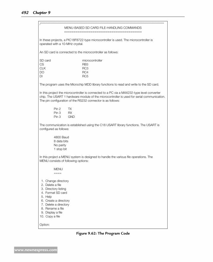
/***************************************************************************************************************MENU-BASED SD CARD FILE-HANDLING COMMANDS=========================================
In these projects, a PIC18F8722-type microcontroller is used. The microcontroller is operated with a 10-MHz crystal.
An SD card is connected to the microcontroller as follows:
SD card microcontrollerCS RB3CLK RC3DO RC4DI RC5
The program uses the Microchip MDD library functions to read and write to the SD card.
In this project the microcontroller is connected to a PC via a MAX232-type level converter chip. The USART 1 hardware module of the microcontroller is used for serial communication. The pin configuration of the RS232 connector is as follows:
Pin 2 TX Pin 3 RX Pin 3 GND
The communication is established using the C18 USART library functions. The USART is configured as follows:
4800 Baud 8 data bits No parity 1 stop bit
In this project a MENU system is designed to handle the various file operations. The MENU consists of following options:
MENU ====
1. Change directory 2. Delete a file 3. Directory listing 4. Format SD card 5. Help 6. Create a directory 7. Delete a directory 8. Rename a file 9. Display a file10. Copy a file
Option:
Figure 9.62: the Program Code
492 Chapter 9
www.newnespress.com
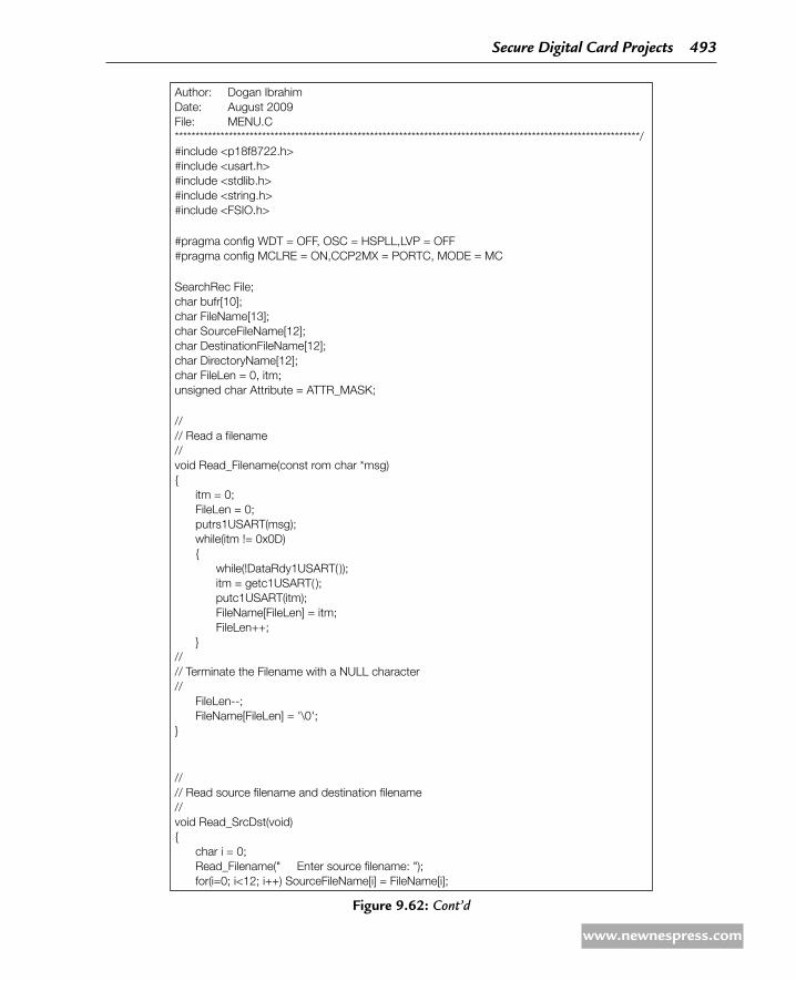
Author: Dogan IbrahimDate: August 2009File: MENU.C****************************************************************************************************************/#include <p18f8722.h>#include <usart.h>#include <stdlib.h>#include <string.h>#include <FSIO.h>
#pragma config WDT = OFF, OSC = HSPLL,LVP = OFF#pragma config MCLRE = ON,CCP2MX = PORTC, MODE = MC
SearchRec File;char bufr[10];char FileName[13];char SourceFileName[12];char DestinationFileName[12];char DirectoryName[12];char FileLen = 0, itm;unsigned char Attribute = ATTR_MASK;
//// Read a filename//void Read_Filename(const rom char *msg) itm = 0; FileLen = 0; putrs1USART(msg); while(itm != 0x0D) while(!DataRdy1USART( )); itm = getc1USART( ); putc1USART(itm); FileName[FileLen] = itm; FileLen++; //// Terminate the Filename with a NULL character// FileLen--; FileName[FileLen] = '\0';
//// Read source filename and destination filename//void Read_SrcDst(void) char i = 0; Read_Filename(" Enter source filename: "); for(i=0; i<12; i++) SourceFileName[i] = FileName[i];
Figure 9.62: Cont’d
secure Digital Card Projects 493
www.newnespress.com

Read_Filename("\n\rEnter destination filename: "); for(i=0; i<12; i++) DestinationFileName[i] = FileName[i];
/* ==================== START OF MAIN PROGRAM ================== *///// Start of MAIN Program//void main(void) FSFILE *pntrs, *pntrd; char Command[6]; char CmdLen, Flag, i; char mode_read[2] = "r"; char mode_write[3] = "w+"; int ReadCnt, Cmd;//// Initialize the USART// Open1USART(USART_TX_INT_OFF & USART_RX_INT_OFF & USART_ASYNCH_MODE & USART_EIGHT_BIT & USART_CONT_RX & USART_BRGH_LOW, 129);//// Display command prompt character $// while(Busy1USART( ));//// ====================== START OF LOOP =======================//while(1) putrs1USART("\n\rOption: ");
//// Read an Option (until the Enter key is pressed)// itm = 0; CmdLen = 0; while(itm != 0x0D) while(!DataRdy1USART( )); itm = getc1USART( ); putc1USART(itm); Command[CmdLen] = itm; CmdLen++; //// Terminate the Command with a NULL character//
Figure 9.62: Cont’d
494 Chapter 9
www.newnespress.com
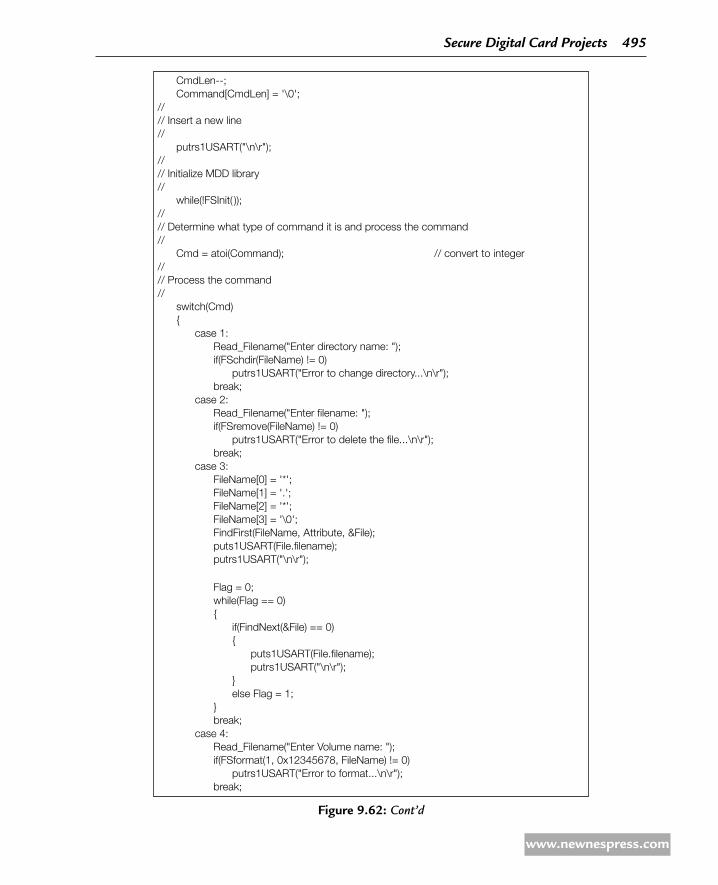
CmdLen--; Command[CmdLen] = '\0';//// Insert a new line// putrs1USART("\n\r"); //// Initialize MDD library// while(!FSInit( ));//// Determine what type of command it is and process the command// Cmd = atoi(Command); // convert to integer//// Process the command// switch(Cmd) case 1: Read_Filename("Enter directory name: "); if(FSchdir(FileName) != 0) putrs1USART("Error to change directory...\n\r"); break; case 2: Read_Filename("Enter filename: "); if(FSremove(FileName) != 0) putrs1USART("Error to delete the file...\n\r"); break; case 3: FileName[0] = '*'; FileName[1] = '.'; FileName[2] = '*'; FileName[3] = '\0'; FindFirst(FileName, Attribute, &File); puts1USART(File.filename); putrs1USART("\n\r");
Flag = 0; while(Flag == 0) if(FindNext(&File) == 0) puts1USART(File.filename); putrs1USART("\n\r"); else Flag = 1; break; case 4: Read_Filename("Enter Volume name: "); if(FSformat(1, 0x12345678, FileName) != 0) putrs1USART("Error to format...\n\r"); break;
Figure 9.62: Cont’d
secure Digital Card Projects 495
www.newnespress.com

case 5: putrs1USART("\n\r MENU\n\r"); putrs1USART( " ====\n\r"); putrs1USART("1. Change directory\n\r"); putrs1USART("2. Delete a file\n\r"); putrs1USART("3. Directory listing\n\r"); putrs1USART("4. Format SD card\n\r"); putrs1USART("5. Help\n\r"); putrs1USART("6. Create a directory\n\r"); putrs1USART("7. Delete a directory\n\r"); putrs1USART("8. Rename a file\n\r"); putrs1USART("9. Display a file\n\r"); putrs1USART("10.Copy a file\n\r"); break; case 6: Read_Filename("Enter directory name: "); if(FSmkdir(FileName) != 0) putrs1USART("Error to create directory...\n\r"); break; case 7: Read_Filename("Enter directory name: "); if(FSrmdir(FileName, 1) != 0) putrs1USART("Error to delete directory...\n\r"); break; case 8: Read_SrcDst( ); pntrs = FSfopen(SourceFileName, mode_read); if(FSrename(DestinationFileName, pntrs) != 0) putrs1USART("Error to rename file...\n\r"); FSfclose(pntrs); break; case 9: Read_Filename("Enter filename: "); pntrs = FSfopen(FileName, mode_read);
ReadCnt = 1; while(ReadCnt != 0) ReadCnt = FSfread(bufr, 1, 10, pntrs); for(i=0; i<ReadCnt; i++) while(Busy1USART( )); putc1USART(bufr[i]); FSfclose(pntrs); break; case 10: Read_SrcDst( ); pntrs = FSfopen(SourceFileName, mode_read); pntrd = FSfopen(DestinationFileName, mode_write);
ReadCnt = 1; while(ReadCnt != 0)
Figure 9.62: Cont’d
496 Chapter 9
www.newnespress.com
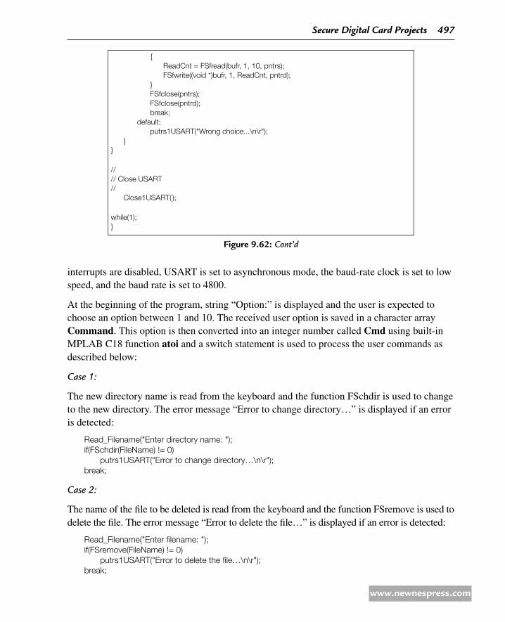
interrupts are disabled, USART is set to asynchronous mode, the baud-rate clock is set to low speed, and the baud rate is set to 4800.
At the beginning of the program, string “Option:” is displayed and the user is expected to choose an option between 1 and 10. The received user option is saved in a character array Command. This option is then converted into an integer number called Cmd using built-in MPLAB C18 function atoi and a switch statement is used to process the user commands as described below:
Case 1:
The new directory name is read from the keyboard and the function FSchdir is used to change to the new directory. The error message “Error to change directory…” is displayed if an error is detected:
Read_Filename("Enter directory name: ");if(FSchdir(FileName) != 0)
putrs1USART("Error to change directory…\n\r");break;
Case 2:
The name of the file to be deleted is read from the keyboard and the function FSremove is used to delete the file. The error message “Error to delete the file…” is displayed if an error is detected:
Read_Filename("Enter filename: ");if(FSremove(FileName) != 0)
putrs1USART("Error to delete the file…\n\r");break;
ReadCnt = FSfread(bufr, 1, 10, pntrs); FSfwrite((void *)bufr, 1, ReadCnt, pntrd); FSfclose(pntrs); FSfclose(pntrd); break; default: putrs1USART("Wrong choice...\n\r");
//// Close USART// Close1USART( );
while(1);
Figure 9.62: Cont’d
secure Digital Card Projects 497
www.newnespress.com

Case 3:
The filename is set to “*.*” and names of all the files (including directory names) in the current working directory are displayed. The function FindFirst is used to find the first file in the directory and the function FindNext is used to find other files in the directory:
FileName[0] = '*';FileName[1] = '.';FileName[2] = '*';FileName[3] = '\0';FindFirst(FileName, Attribute, &File);puts1USART(File.filename);putrs1USART("\n\r");
Flag = 0;while(Flag == 0)
if(FindNext(&File) == 0)
puts1USART(File.filename);putrs1USART("\n\r");
else Flag = 1;
break;
Case 4:
This option reads the required volume name from the keyboard and formats the SD card by giving the card this volume name. The error message “Error to format…” is displayed if an error is detected:
Read_Filename("Enter Volume name: ");if(FSformat(1, 0x12345678, FileName) != 0)
putrs1USART("Error to format…\n\r");break;
Case 5:
This option displays the MENU items:
putrs1USART("\n\r MENU\n\r");putrs1USART( " ====\n\r");putrs1USART("1. Change directory\n\r");putrs1USART("2. Delete a file\n\r");putrs1USART("3. Directory listing\n\r");putrs1USART("4. Format SD card\n\r");putrs1USART("5. Help\n\r");putrs1USART("6. Create a directory\n\r");putrs1USART("7. Delete a directory\n\r");putrs1USART("8. Rename a file\n\r");
498 Chapter 9
www.newnespress.com

putrs1USART("9. Display a file\n\r");putrs1USART("10.Copy a file\n\r");break;
Case 6:
This function reads a directory name and creates a directory with this name using the function FSmkdir. The error message “Error to create directory…” is displayed if an error is detected:
Read_Filename("Enter directory name: ");if(FSmkdir(FileName) != 0)
putrs1USART("Error to create directory…\n\r");break;
Case 7:
This option reads a directory name and then this directory is deleted from the current work-ing directory using the function FSrmdir. The error message “Error to delete directory…” is displayed if an error is detected:
Read_Filename("Enter directory name: ");if(FSrmdir(FileName, 1) != 0)
putrs1USART("Error to delete directory…\n\r");break;
Case 8:
This option changes the name of a file. The user function Read_SrcDst is called to read the destination and the source filenames, and then the MDD function FSrename is used to rename the file. Note that the source file must be opened with read attribute and its file pointer must be used in the FSrename function. The error message “Error to rename file…” is displayed if an error is detected:
Read_SrcDst( );pntrs = FSfopen(SourceFileName, mode_read);if(FSrename(DestinationFileName, pntrs) != 0)
putrs1USART("Error to rename file…\n\r");FSfclose(pntrs);break;
Case 9:
This option displays a file on the PC screen. The filename is read from the keyboard and the file is opened in read mode. Then, a while loop is formed to read and display the contents of the file until the end of file is reached:
Read_Filename("Enter filename: ");pntrs = FSfopen(FileName, mode_read);
ReadCnt = 1;
secure Digital Card Projects 499
www.newnespress.com

while(ReadCnt != 0)
ReadCnt = FSfread(bufr, 1, 10, pntrs);for(i=0; i<ReadCnt; i++)
while(Busy1USART( ));putc1USART(bufr[i]);
FSfclose(pntrs);break;
Case 10:
This option copies one file to another file. The user function Read_SrcDst is called to read the source and the destination filenames. Then the source file is opened in read mode and the destination file is opened in write mode. A while loop is formed, and the data is read from the source file and written into the destination file until the end of the source file is reached. At the end, both the source file and the destination file are closed:
Read_SrcDst( );pntrs = FSfopen(SourceFileName, mode_read);pntrd = FSfopen(DestinationFileName, mode_write);
ReadCnt = 1;while(ReadCnt != 0)
ReadCnt = FSfread(bufr, 1, 10, pntrs);FSfwrite((void *)bufr, 1, ReadCnt, pntrd);
FSfclose(pntrs);FSfclose(pntrd);break;
Default:
This option of the switch statement is executed if the user option is not between 1 and 10:
putrs1USART("Wrong choice…\n\r");
Figures 9.63 and 9.64 show typical outputs from the project.
In the program code in Figure 9.62, the error messages are displayed by checking the return values of the MDD functions. The MDD library provides a function called FSerror that can be used to find the exact cause of a problem when an error occurs in a previous MDD function call. FSerror returns an integer where the actual error messages can be found in the MDD documentation (e.g., the Release Notes for Microchip Memory Disk Drive File System, Version 1.2.0, August 20, 2008).
An example for the use of function FSerror is shown in Figure 9.65, where the MDD func-tion FSremove is used to delete a file from the current working directory. For example,
500 Chapter 9
www.newnespress.com

Figure 9.63: typical Output from the Project
Figure 9.64: typical Output from the Project
secure Digital Card Projects 501
www.newnespress.com

if the file to be deleted is not found in the directory, the error message “The specified file could not be found” will be displayed (see the MDD documentation for a full list of error messages).
9168 suggestions for Future Work
Write a program, similar to the program given in this project, but include all the FSerror-based error messages in your program.
9.17 PrOJeCt 16 – digital data Logging to Sd Card
9171 Description
This project is about data logging of digital data to the SD card. In this project, microcontrol-ler’s PORTE and PORTF data are collected every second and stored on the SD card in a file called DIGITAL.TXT in hexadecimal format. The data items are separated with a comma so that the data is compatible with Excel spreadsheet and can be imported into Excel, if required for further processing.
An active low push-button Start/Stop switch is provided (connected to RB0) to control oper-ation of the program. Data collection starts when the switch is pressed. The program stops when the switch is pressed for a few seconds so that the SD card can be removed safely.
case 2: Read_Filename("Enter filename: "); Ret = FSremove(FileName); if(Ret != 0) Error = FSerror( );
switch(Error) case CE_WRITE_PROTECTED: putrs1USART("Devide write protected...\n\r"); break; case CE_FILE_NOT_FOUND: putrs1USART("The specified file is not found...\n\r"); break; case CE_INVALID_FILENAME: putrs1USART("Specified filename was invalid...\n\r"); break; case CE_ERASE_FAIL: putrs1USART("The file could not be erased...\n\r"); break;
Figure 9.65: Using the FSerror Function
502 Chapter 9
www.newnespress.com

9172 Aim
The aim of this project is to show how digital data can be collected and stored on the SD card every second.
9173 Block Diagram
The block diagram of this project is shown in Figure 9.66.
9174 Circuit Diagram
The circuit diagram of this project is shown in Figure 9.67.
9175 Operation of the Project
The operation of the project is shown in Figure 9.68.
9176 Program Code
The program code (DIGLOG.C) is shown in Figure 9.69.
9177 Description of the Program Code
At the beginning of the program, the port directions are configured and the program waits until the Start/Stop button is pressed. After the button is pressed and released, the MDD library is initialized and a new file called DIGITAL.TXT is created on the SD card. The main part of the program is in a while loop. Inside this loop, data from PORTE and PORTF are read and stored in the file using the MDD function FSfprint. Data is written to the file in the hexadecimal format and is separated with a comma. The program then checks whether or not the Start/Stop button is pressed to stop the program, and if so, the file is closed and the program stops waiting in a while loop forever.
Figure 9.66: Block diagram of the Project
PICmicro-
controller
RB0
PORT EPORT F
Start/Stop
Digitalinputs
SDcard
secure Digital Card Projects 503
www.newnespress.com
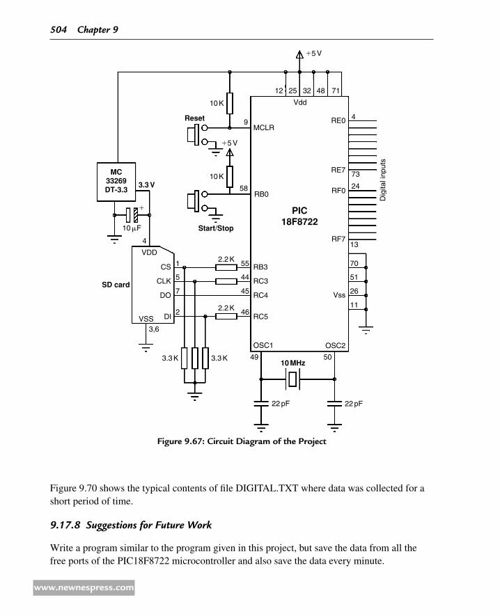
Figure 9.70 shows the typical contents of file DIGITAL.TXT where data was collected for a short period of time.
9178 suggestions for Future Work
Write a program similar to the program given in this project, but save the data from all the free ports of the PIC18F8722 microcontroller and also save the data every minute.
Figure 9.67: Circuit diagram of the Project
Reset
10 K
10 K
9
MC33269DT-3.3
3.3 V
1
10 mF
4
DI
DO
CLK
CS
VDD
VSS3,6
5
7
2
3.3 K3.3 K
RB355
58
44
45
462.2 K
2.2 K1
RC3
RC4
RC5
PIC18F8722
MCLR
15 V
15 V
12 25 32 48 71
Vdd
SD card
Start/Stop
OSC1 OSC2
5049
22 pF 22 pF
10 MHz
RE0 4
73
24
70
51
26
11
13
RE7
Dig
ital i
nput
s
RF7
Vss
RF0RB0
504 Chapter 9
www.newnespress.com

BEGIN Initialise the MDD library Open new file on SD card Wait until START/STOP button is pressed DO FOREVER Read PORT B and PORT D data Store data in file (separated with a comma) IF Start/Stop button is pressed Close file Wait here forever ENDIF Wait a second ENDDOEND
Figure 9.68: Operation of the Project
Figure 9.69: the Program Code
/*************************************************************************************************************DIGITAL DATA LOGGING USING SD CARD===============================
In these projects, a PIC18F8722-type microcontroller is used. The microcontrolleris operated with a 10-MHz crystal.
An SD card is connected to the microcontroller as follows:
SD card microcontrollerCS RB3CLK RC3DO RC4DI RC5
The program uses the Microchip MDD library functions to read and write to the SD card.
This is a digital data logging project where digital data from ports PORT E and PORT F are read and stored on the SD card in a file called DIGITAL.TXT every second. The data items are separated with a comms so that the data is compatible with most spreadsheetprograms.
Author: Dogan IbrahimDate: August 2009File: DIGLOG.C*************************************************************************************************************/#include <p18f8722.h>#include <stdlib.h>#include <string.h>#include <delays.h>#include <FSIO.h>
#pragma config WDT = OFF, OSC = HSPLL,LVP = OFF#pragma config MCLRE = ON,CCP2MX = PORTC, MODE = MC
#define STRT PORTBbits.RB0
secure Digital Card Projects 505
www.newnespress.com

void main(void) FSFILE *pntr; int PortEData, PortFData,i;//// Configure PORTS E and PORT F to digital inputs// TRISE = 0xFF; TRISF = 0xFF; TRISB = 1; ADCON1 = 0xFF;//// Wait until START BUTTON is pressed and released// while(STRT); while(!STRT);//// Initialize MDD library// while(!FSInit( ));//// Open file DIGITAL.TXT in write mode (create it)// pntr = FSfopenpgm("DIGITAL.TXT", "w+");//// ======================= START OF LOOP =======================//// Read PORT E and PORT F data and store in file//while(1) PortEData = PORTE; PortFData = PORTF;//// Write to SD card// FSfprintf(pntr, "%02X, %02X\n", PortEData, PortFData);//// Check if BUTTON is pressed and if so, close the file and stop the program// if(STRT == 0) FSfclose(pntr); while(1); //// Wait for a second. Clock freq = 40 MHz, clock cycle = 0.1 microsecond// The basic delay with Delay10KTCYx is 1ms. With a count of 1000 // the delay is 1 second. A loop is formed to iterate 4 times // for the required delay of 1 second // for(i=0; i< 4; i++)Delay10KTCYx(250);
Figure 9.69: Cont’d
506 Chapter 9
www.newnespress.com

Figure 9.70: typical diGitaL.tXt File
20, 4F20, 4E20, 4E23, 4020, 4C22, 4D21, 4223, 4A0E, 440F, 441F, 42
9.18 PrOJeCt 17 – temperature data Logging
9181 Description
This project is about data logging of the ambient temperature data on the SD card every second. An analog temperature sensor IC (MCP9701A) is used to sense the ambient temperature and is connected to port RA1 of the PIC18F8722 microcontroller. A file called TEMP.TXT is created on the SD card, and the temperature is stored in this file every second, one data item on each line, with each data item followed by a new-line character.
An active low push-button Start/Stop switch is provided (connected to RB0) to control operation of the program. Data collection starts when the switch is pressed. The program stops when the switch is pressed for a few seconds so that the SD card can be removed safely.
9182 Aim
The aim of this project is to show how analog data can be collected and stored on the SD card every second.
9183 Block Diagram
The block diagram of this project is shown in Figure 9.71.
9184 Circuit Diagram
The circuit diagram of this project is shown in Figure 9.72. The PICDEM PIC18 Explorer board is equipped with an MCP9701A temperature sensor IC connected to port RA1 of the microcontroller. Thus, the board can be used with this project without any hardware changes.
secure Digital Card Projects 507
www.newnespress.com
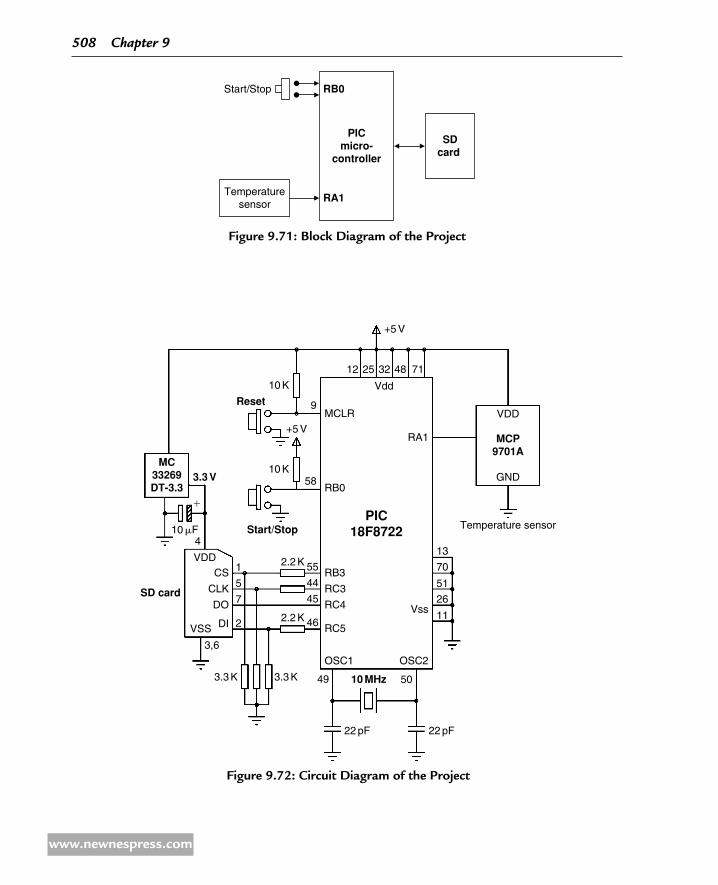
Figure 9.71: Block diagram of the Project
Temperaturesensor
PICmicro-
controller
RB0
RA1
Start/Stop
SDcard
Figure 9.72: Circuit diagram of the Project
Reset
3.3 V
SD card
MC33269DT-3.3
MCP9701A
Start/StopPIC
18F8722
10 MHz
+5 V
12 25 32
Vdd
RA1
9
58
551
5
7
2
44
45
46
49
10 K
10 mF
1
4
VDD
VDD
GND
Temperature sensor
13
70
51
26
11
22 pF22 pF
VSS
CS
CLK
DO
DI
2.2 K
2.2 K
3,6
3.3 K 3.3 K
+5 V
48 71
MCLR
RB0
RB3
RC3
RC4
RC5
OSC1 OSC2
50
Vss
10 K
508 Chapter 9
www.newnespress.com
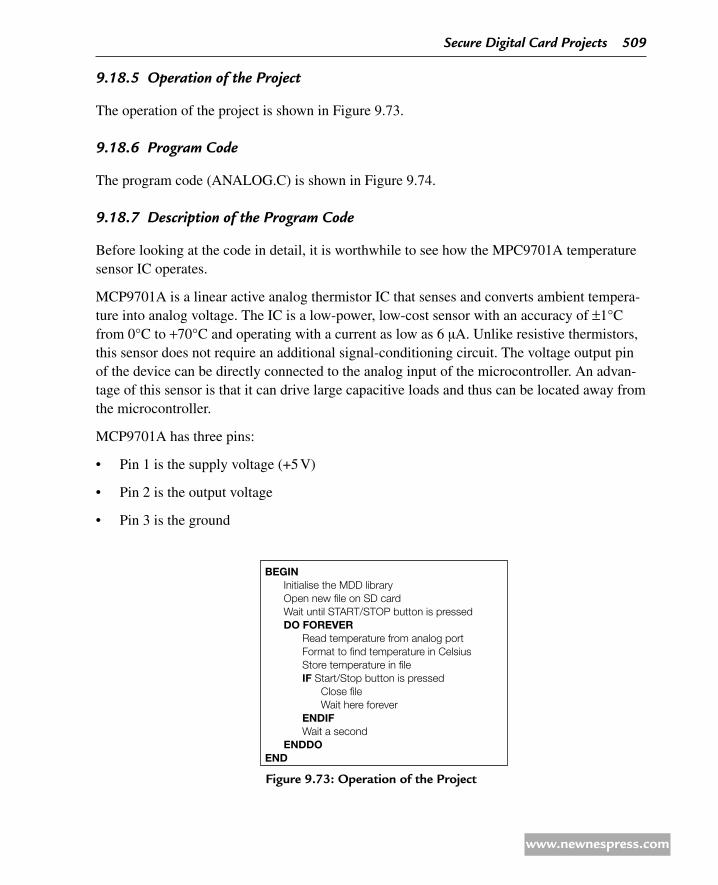
9185 Operation of the Project
The operation of the project is shown in Figure 9.73.
9186 Program Code
The program code (ANALOG.C) is shown in Figure 9.74.
9187 Description of the Program Code
Before looking at the code in detail, it is worthwhile to see how the MPC9701A temperature sensor IC operates.
MCP9701A is a linear active analog thermistor IC that senses and converts ambient tempera-ture into analog voltage. The IC is a low-power, low-cost sensor with an accuracy of ±1°C from 0°C to +70°C and operating with a current as low as 6 μA. Unlike resistive thermistors, this sensor does not require an additional signal-conditioning circuit. The voltage output pin of the device can be directly connected to the analog input of the microcontroller. An advan-tage of this sensor is that it can drive large capacitive loads and thus can be located away from the microcontroller.
MCP9701A has three pins:
Pin 1 is the supply voltage (+5 V) •
Pin 2 is the output voltage •
Pin 3 is the ground •
Figure 9.73: Operation of the Project
BEGIN Initialise the MDD library Open new file on SD card Wait until START/STOP button is pressed DO FOREVER Read temperature from analog port Format to find temperature in Celsius Store temperature in file IF Start/Stop button is pressed Close file Wait here forever ENDIF Wait a second ENDDOEND
secure Digital Card Projects 509
www.newnespress.com
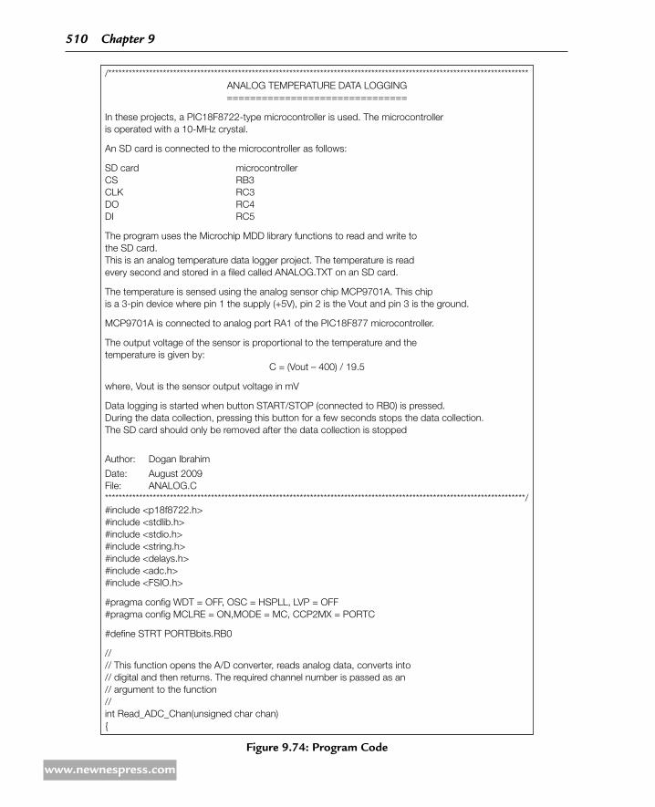
Figure 9.74: Program Code
/***************************************************************************************************************************ANALOG TEMPERATURE DATA LOGGING===============================
In these projects, a PIC18F8722-type microcontroller is used. The microcontrolleris operated with a 10-MHz crystal.
An SD card is connected to the microcontroller as follows:
SD card microcontrollerCS RB3CLK RC3DO RC4DI RC5
The program uses the Microchip MDD library functions to read and write to the SD card.This is an analog temperature data logger project. The temperature is read every second and stored in a filed called ANALOG.TXT on an SD card.
The temperature is sensed using the analog sensor chip MCP9701A. This chip is a 3-pin device where pin 1 the supply (+5V), pin 2 is the Vout and pin 3 is the ground.
MCP9701A is connected to analog port RA1 of the PIC18F877 microcontroller.
The output voltage of the sensor is proportional to the temperature and the temperature is given by:
C = (Vout – 400) / 19.5
where, Vout is the sensor output voltage in mV
Data logging is started when button START/STOP (connected to RB0) is pressed. During the data collection, pressing this button for a few seconds stops the data collection. The SD card should only be removed after the data collection is stopped
Author: Dogan Ibrahim
Date: August 2009File: ANALOG.C***************************************************************************************************************************/#include <p18f8722.h>#include <stdlib.h>#include <stdio.h>#include <string.h>#include <delays.h>#include <adc.h>#include <FSIO.h>
#pragma config WDT = OFF, OSC = HSPLL, LVP = OFF#pragma config MCLRE = ON,MODE = MC, CCP2MX = PORTC
#define STRT PORTBbits.RB0
//// This function opens the A/D converter, reads analog data, converts into// digital and then returns. The required channel number is passed as an// argument to the function//int Read_ADC_Chan(unsigned char chan)
510 Chapter 9
www.newnespress.com
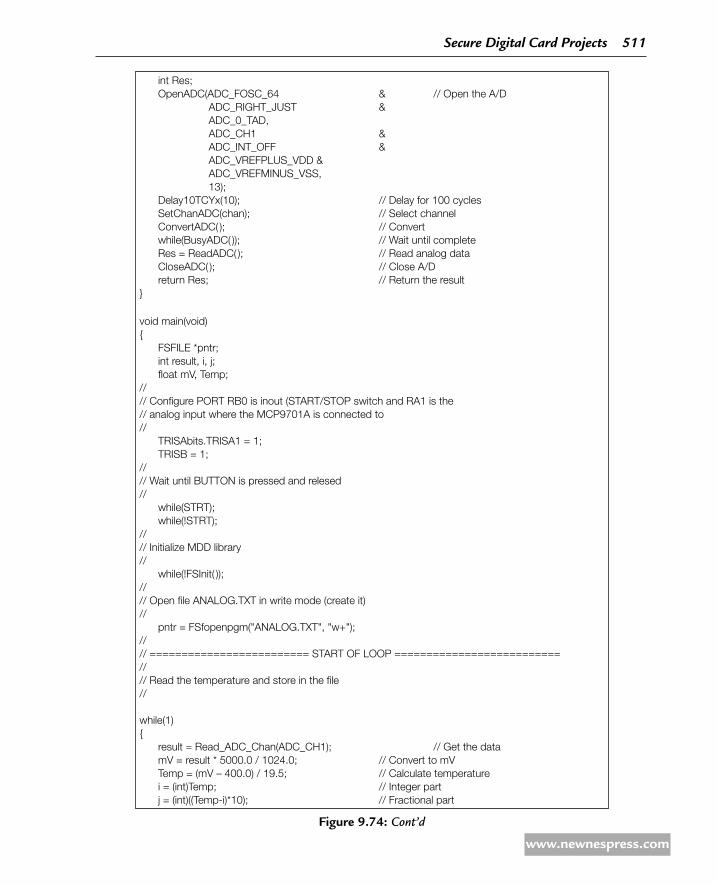
int Res; OpenADC(ADC_FOSC_64 & // Open the A/D ADC_RIGHT_JUST & ADC_0_TAD, ADC_CH1 & ADC_INT_OFF & ADC_VREFPLUS_VDD & ADC_VREFMINUS_VSS, 13); Delay10TCYx(10); // Delay for 100 cycles SetChanADC(chan); // Select channel ConvertADC( ); // Convert while(BusyADC( )); // Wait until complete Res = ReadADC( ); // Read analog data CloseADC( ); // Close A/D return Res; // Return the result
void main(void) FSFILE *pntr; int result, i, j; float mV, Temp;//// Configure PORT RB0 is inout (START/STOP switch and RA1 is the// analog input where the MCP9701A is connected to// TRISAbits.TRISA1 = 1; TRISB = 1;//// Wait until BUTTON is pressed and relesed// while(STRT); while(!STRT);//// Initialize MDD library// while(!FSInit( ));//// Open file ANALOG.TXT in write mode (create it)// pntr = FSfopenpgm("ANALOG.TXT", "w+");//// ========================= START OF LOOP ==========================//// Read the temperature and store in the file//
while(1) result = Read_ADC_Chan(ADC_CH1); // Get the data mV = result * 5000.0 / 1024.0; // Convert to mV Temp = (mV – 400.0) / 19.5; // Calculate temperature i = (int)Temp; // Integer part j = (int)((Temp-i)*10); // Fractional part
Figure 9.74: Cont’d
secure Digital Card Projects 511
www.newnespress.com

//// Write to SD card// FSfprintf(pntr, "%d.%d\n", i, j);//// Check if BUTTON is pressed and if so, close the file and stop the program// if(STRT == 0) FSfclose(pntr); while(1); //// Wait for a second. Clock freq = 40 MHz, clock cycle = 0.1 microsecond// The basic delay with Delay10KTCYx is 1ms. With a count of 1000, the// delay is 1 second. A loop is formed to iterate 4 times for the required delay// of 1 second //
for(i=0; i< 4; i++)Delay10KTCYx(250);
Figure 9.74: Cont’d
The output voltage Vo of MCP9701A is proportional to the ambient temperature and the relationship is given by
Vo = TC × TA + V0C ,
where Vo is the sensor output voltage, TC is the sensor temperature coefficient, TA is the ambient temperature, and V0C is the sensor output voltage at 0°C.
From the manufacturer’s specifications,
TC = 19.5 mV/°C
V0C = 400 mV
Thus, we can write the equation as
Vo = 400 + 19.5 C,
where Vo is the sensor output voltage (mV) and C is the ambient temperature in °C.
Rearranging the formula, we get
C = Vo − 400 19.5
Figure 9.75 shows change of the output voltage with the ambient temperature.
512 Chapter 9
www.newnespress.com

The steps to calculate the temperature are as follows:
Read the output voltage of the sensor using the A/D converter •
Convert the voltage to mV •
Use the above formula to calculate the temperature in °C •
At the beginning of the program (see Figure 9.74), analog port pin RA1 and digital port pin RB0 are configured as inputs. The program then waits until the Start/Stop switch is pressed, and after the switch is released, the MDD library is initialized and new file ANALOG.TXT is created on the SD card. The main program loop starts with a while loop where the following code is executed every second inside the loop.
Temperature data is read from analog port RA1 by calling the function Read_ADC_Chan. •The port number is passed as an argument to the function. The function opens the ADC port using a clock frequency Fosc/64, the data is right-justified, interrupts are disabled, and port RA1 is configured as analog port. The C18 function SetChanADC selects the channel CH1 and then the function ConvertADC is called to start the A/D conversion, and the code waits until the conversion is ready. Once the data is converted, it is read from the A/D module by calling the function ReadADC, and the result is returned by the function to the calling program:
OpenADC(ADC_FOSC_64 & ADC_RIGHT_JUST & ADC_0_TAD, ADC_CH1 & ADC_INT_OFF & ADC_VREFPLUS_VDD & ADC_VREFMINUS_VSS, 13);
Figure 9.75: Change of Output Voltage with ambient temperature
400
600
800
1000
1200
1400
1600
1800
0 20 40 60 80Temperature, C
Vo
ltag
e, m
V
secure Digital Card Projects 513
www.newnespress.com

Delay10TCYx(10); // Delay for 100 cyclesSetChanADC(chan); // Select channelConvertADC( ); // Convertwhile(BusyADC( )); // Wait until completeRes = ReadADC( ); // Read analog dataCloseADC( ); // Close A/Dreturn Res; // Return the result
The converted data is multiplied by 5000 and divided by 1024 to obtain the temperature •data in millivolts. The physical temperature is then calculated in °C using the derived formula and stored in variable Temp:
result = Read_ADC_Chan(ADC_CH1); // Get the datamV = result * 5000.0 / 1024.0; // Convert to mVTemp = (mV − 400.0) / 19.5; // Calculate temperature
The decimal part of the temperature is stored in the variable i and the fractional part •is stored in the variable j. In this program, only one digit is used after the decimal point:
i = (int)Temp; // Integer partj = (int)((Temp−i)*10); // Fractional part
The temperature data is then written to the file using the MDD function FSfprintf: •
FSfprintf(pntr, "%d.%d\n", i, j);
The program then checks whether or not the Start/Stop button is pressed and if so closes •the file and stops the program; otherwise, the above steps are repeated after a 1-s delay.
Figure 9.76 shows contents of file ANALOG.TXT for a typical run of the program.
Figure 9.76: typical aNaLOG.tXt File
26.826.325.426.626.227.529.328.528.526.828.829.029.029.029.029.3
514 Chapter 9
www.newnespress.com

9188 suggestions for Future Work
Write a program similar to the program given in this project, but use two temperature sensors and save the data from both the sensors in the same file every minute.
9.19 PrOJeCt 18 – temperature and Pressure data Logging with real-time Clock
9191 Description
This project is about data logging of temperature and pressure data on the SD card every second with real-time clock data. As in the previous project, an analog temperature sensor IC (MCP9701A) is used to sense the ambient temperature and is connected to port RA1 of the PIC18F8722 microcontroller. In addition, a pressure sensor IC (MPX4115A), connected to port RA2, is used to measure the ambient pressure. The temperature and the pressure data are stored in files TEMP.DAT and PRESS.DAT, respectively.
A real-time clock is made up in software using timer TMR0 of the microcontroller. The clock software is updated every second and keeps the absolute date and time information as long as the program is running. The clock is loaded from the PC by entering the current date and time from the keyboard.
An active low push-button Start/Stop/Configure switch is provided (connected to RB0) to control the operation of the program. The program operates in three modes: Configuration mode, Run mode, and Stop mode. The Configuration mode is entered when the Start/Stop/Configure button is pressed after the microcontroller is turned on or after the master reset is applied. During this mode, the user enters the real-time date and clock data. Pressing the Start/Stop/Configure button again places the program in the Run mode. In this mode, data is col-lected from the temperature and pressure sensors and stored in the files on the SD card every second. Pressing the Start/Stop/Configure button for a few seconds places the program into Stop mode where the files on the SD card are closed and the card can be removed safely from its holder.
9192 Aim
The aim of this project is to show how multiple analog data can be collected and stored on the SD card continuously. In addition, the project shows how a real-time clock can be imple-mented in software.
9193 Block Diagram
The block diagram of this project is shown in Figure 9.77.
secure Digital Card Projects 515
www.newnespress.com

9194 Circuit Diagram
The circuit diagram of this project is shown in Figure 9.78. The temperature sensor and the pressure sensor ICs are connected to analog ports RA1 and RA2 of the micro-controller, respectively. The project is based on a PIC18F8722 microcontroller, and a 10-MHz crystal is used to provide clock pulses to the microcontroller. The serial port is connected to port pins TXD and RXD of the microcontroller via a MAX232-type RS232 level converter chip.
9195 Operation of the Project
The operation of the project is shown in Figure 9.79.
9196 Program Code
The program code (LOG.C) is shown in Figure 9.80.
9197 Description of the Program Code
Before looking at the code in detail, it is worthwhile to see how the MPX4115A pressure sensor IC operates.
MPX4115A is a 6- or 8-pin pressure sensor IC that provides an output voltage proportional to the ambient atmospheric pressure. The pin configurations are as follows:
Figure 9.81 shows the 6-pin MPX4115A pressure sensor chip.
Pins descriptions
6-pin sensor
1 Output voltage
2 Ground
3 +5-V supply
4–6 Not used
8-pin sensor
1 Not used
2 +5-V supply
3 Ground
4 Output voltage
5–8 Not used
516 Chapter 9
www.newnespress.com

Figure 9.78: Circuit diagram of the Project
15 V
Vdd
Vcc
V1DIN1
DOUT1 1461
2738495
13
ROUT1
MAX232
12C BUS
V2
Gnd
RIN1
C11 C12
C21 C22
TXD37
1 mF
1 mF
To PC serial port15 4 5
1 mF
38 126
11
16 1 3
2
RXD
MCLR9
58
29
28
554445
46
49 50
2.2 K
3.3 K 3.3 K
2.2 KCS 1
57
2
CLKDO
DI3,6
VDDVSS
10 K10 K
Start/Stop/Configure
MCP9701ATemp
sensor
Pressuresensor
MPX4115A
3.3 V
SD card
10 mF
41
MC33269DT-3.3
Reset
RB0
RA1
RA2
RB3RC3RC4
RC5
OSC1 OSC2
Vss
12 25 32 48 71
22 pF22 pF
10 MHz
70512611
PIC18F8722
1 mF
Figure 9.77: Block diagram of the Project
Temperaturesensor
PICmicro-
controller
RB0
RA1
Start/Stop/Configure
SDcard
PCPressuresensor
RA2
secure Digital Card Projects 517
www.newnespress.com
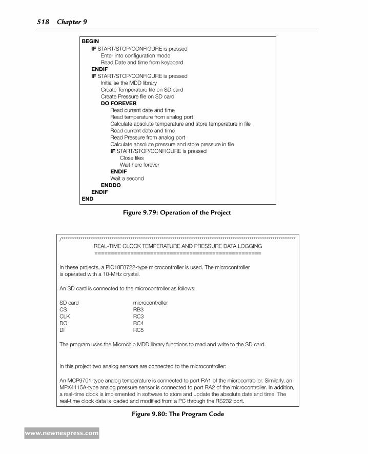
Figure 9.79: Operation of the Project
BEGIN IF START/STOP/CONFIGURE is pressed Enter into configuration mode Read Date and time from keyboard ENDIF IF START/STOP/CONFIGURE is pressed Initialise the MDD library Create Temperature file on SD card Create Pressure file on SD card DO FOREVER Read current date and time Read temperature from analog port Calculate absolute temperature and store temperature in file Read current date and time Read Pressure from analog port Calculate absolute pressure and store pressure in file IF START/STOP/CONFIGURE is pressed Close files Wait here forever ENDIF Wait a second ENDDO ENDIFEND
/**************************************************************************************************************************REAL-TIME CLOCK TEMPERATURE AND PRESSURE DATA LOGGING===================================================
In these projects, a PIC18F8722-type microcontroller is used. The microcontrolleris operated with a 10-MHz crystal.
An SD card is connected to the microcontroller as follows:
SD card microcontrollerCS RB3CLK RC3DO RC4DI RC5
The program uses the Microchip MDD library functions to read and write to the SD card.
In this project two analog sensors are connected to the microcontroller:
An MCP9701-type analog temperature is connected to port RA1 of the microcontroller. Similarly, an MPX4115A-type analog pressure sensor is connected to port RA2 of the microcontroller. In addition, a real-time clock is implemented in software to store and update the absolute date and time. The real-time clock data is loaded and modified from a PC through the RS232 port.
Figure 9.80: the Program Code
518 Chapter 9
www.newnespress.com

Two files are created on the SD card: TEMP.DAT and PRESS.DAT store the temperature and pressure data, respectively.
MCP9701A chip is a 3-pin device where pin 1 is the supply (+5V), pin 2 is the Vout and pin 3 is the ground.
The output voltage of the sensor is proportional to the temperature and is given by:
C = (Vout – 400) / 19.5
where, Vout is the sensor output voltage in mV
MPX4115 chip is a 6- or 8-pin chip. The 6-pin version is used in this project with the following pin configuration:
Pin 1 Output voltage Pin 2 Ground Pin 3 +5V supply Pins 4-6 not used
The output voltage of MPX4115 is proportional to the atmospheric pressure and is given by:
mb = (2.0V + 0.95)/0.009
where mb is the pressure in millibars and V is the sensor output voltage.
The system has three modes of operation: the Configuration Mode, Run mode, and the STOP mode. The Configuration Mode is entered when button START/STOP/CONFIGURE is pressed. Current date and time are entered from the PC keyboard and stored and updated every second in the program.
When the START/STOP/CONFIGURATION button is pressed the program enters the RUN mode where data is collected every second from the two sensors and stored in files on the SD card every second.
When the START/STOP/CONFIGURE button is held down for a few seconds the program enters the STOP mode where the files are closed on the SD card and thus the SD card can be removed from its holder.
Author: Dogan IbrahimDate: August 2009File: LOG.C**************************************************************************************************************************/#include <p18f8722.h>#include <stdlib.h>#include <stdio.h>#include <string.h>#include <delays.h>#include <adc.h>#include <usart.h>#include <i2c.h>#include <FSIO.h>
Figure 9.80: Cont’d
secure Digital Card Projects 519
www.newnespress.com

#pragma config WDT = OFF, OSC = HSPLL, LVP = OFF#pragma config MCLRE = ON,MODE = MC, CCP2MX = PORTC
#define STRT PORTBbits.RB0#define NUM(x,y) (10*(x - '0') + y - '0')#define MSD(x) ((x / 10 + '0'))#define LSD(x) ((x % 10) + '0')
unsigned char DateTime[ ] = "12/10/09 10:00:00 ";unsigned char One_Sec_Flag;unsigned char Days[ ]=0,31,28,31,30,31,30,31,31,30,31,30,31;
void One_Second_Delay(void);void timer_ISR(void);
//// Define the high interrupt vector to be at 0x08//#pragma code high_vector=0x08 // Following code at void address 0x08 interrupt(void)
_asm GOTO timer_ISR _endasm // Jump to ISR#pragma code // Return to default code section
//// timer_ISR is an interrupt service routine (jumps here every 5ms)//#pragma interrupt timer_ISRvoid timer_ISR( ) One_Sec_Flag = 1; // Set One_Sec_Flag TMR0L = 0x69; // Re-load TMR0 TMR0H = 0x67; // Re-Load TMR0H INTCON = 0x20; // Set T0IE and clear T0IF
//// This function opens the A/D converter, reads analog data, converts into // digital and then returns. The required channel number is passed as an // argument to the function//int Read_ADC_Chan(unsigned char chan) int Res;
OpenADC(ADC_FOSC_64 & // Open the A/D ADC_RIGHT_JUST & ADC_0_TAD, ADC_CH1 & ADC_INT_OFF &
Figure 9.80: Cont’d
520 Chapter 9
www.newnespress.com
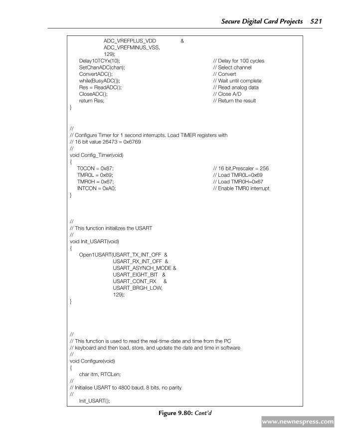
ADC_VREFPLUS_VDD & ADC_VREFMINUS_VSS, 129); Delay10TCYx(10); // Delay for 100 cycles SetChanADC(chan); // Select channel ConvertADC( ); // Convert while(BusyADC( )); // Wait until complete Res = ReadADC( ); // Read analog data CloseADC( ); // Close A/D return Res; // Return the result
//// Configure Timer for 1 second interrupts. Load TIMER registers with // 16 bit value 26473 = 0x6769//void Config_Timer(void) T0CON = 0x87; // 16 bit,Prescaler = 256 TMR0L = 0x69; // Load TMR0L=0x69 TMR0H = 0x67; // Load TMR0H=0x67 INTCON = 0xA0; // Enable TMR0 interrupt
//// This function initializes the USART//void Init_USART(void) Open1USART(USART_TX_INT_OFF & USART_RX_INT_OFF & USART_ASYNCH_MODE & USART_EIGHT_BIT & USART_CONT_RX & USART_BRGH_LOW, 129);
//// This function is used to read the real-time date and time from the PC// keyboard and then load, store, and update the date and time in software//void Configure(void) char itm, RTCLen;//// Initialise USART to 4800 baud, 8 bits, no parity// Init_USART( );
Figure 9.80: Cont’d
secure Digital Card Projects 521
www.newnespress.com
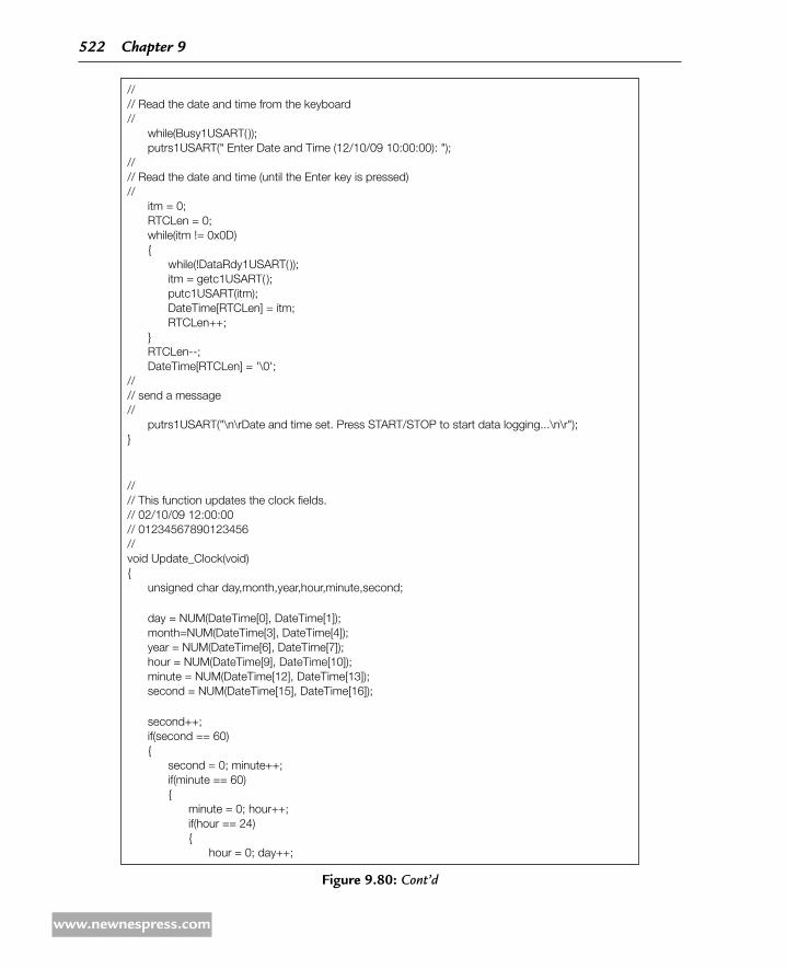
//// Read the date and time from the keyboard// while(Busy1USART( )); putrs1USART(" Enter Date and Time (12/10/09 10:00:00): ");//// Read the date and time (until the Enter key is pressed)// itm = 0; RTCLen = 0; while(itm != 0x0D) while(!DataRdy1USART( )); itm = getc1USART( ); putc1USART(itm); DateTime[RTCLen] = itm; RTCLen++; RTCLen--; DateTime[RTCLen] = '\0';//// send a message// putrs1USART("\n\rDate and time set. Press START/STOP to start data logging...\n\r");
//// This function updates the clock fields.// 02/10/09 12:00:00// 01234567890123456//void Update_Clock(void) unsigned char day,month,year,hour,minute,second;
day = NUM(DateTime[0], DateTime[1]); month=NUM(DateTime[3], DateTime[4]); year = NUM(DateTime[6], DateTime[7]); hour = NUM(DateTime[9], DateTime[10]); minute = NUM(DateTime[12], DateTime[13]); second = NUM(DateTime[15], DateTime[16]);
second++; if(second == 60) second = 0; minute++; if(minute == 60) minute = 0; hour++; if(hour == 24) hour = 0; day++;
Figure 9.80: Cont’d
522 Chapter 9
www.newnespress.com

if(day == Days[month]+1) day = 1; month++; if(month == 13) month = 1; year++; DateTime[15] = MSD(second); DateTime[16] = LSD(second); DateTime[12] = MSD(minute); DateTime[13] = LSD(minute); DateTime[9] = MSD(hour); DateTime[10] = LSD(hour); DateTime[6] = MSD(year); DateTime[7] = LSD(year); DateTime[3] = MSD(month); DateTime[4] = LSD(month); DateTime[0] = MSD(day); DateTime[1] = LSD(day);
void main(void) FSFILE *pntrTemp, *pntrPress; int result, i, j; float mV, Temp, Press;//// Configure PORT RB0 is inout (START/STOP switch, RA1, and RA2 are the// analog inputs where the MCP9701A and MPX4115A are connected to// TRISAbits.TRISA1 = 1; // RA1 is input TRISAbits.TRISA2 = 1; // RA2 is input TRISBbits.TRISB0 = 1; // RB0 is input
//// Check if START/STOP button is pressed and if so enter the Configuration mode,// read the clock data and wait until START/STOP button is pressed and then// continue to data logging// One_Sec_Flag = 0;
while(STRT); // Wait until button pressed while(!STRT); // // Enter Configuration mode. Wait until the button is released // and call function Configure to read the real time date and time. // Configure( );
Figure 9.80: Cont’d
secure Digital Card Projects 523
www.newnespress.com

Figure 9.80: Cont’d
//// Configure Timer. Start timer interrupts// Config_Timer( );//// Look for leap year and adjust for February// result = 10*(DateTime[6] - '0') + DateTime[7] - '0'; result = result % 4; if(result == 0) Days[2] = 29; else Days[2] = 28;//// Wait until the START/STOP button is pressed and if so enter the Run mode. // In this mode data is collected from the sensors and stored in two files // on the SD card// while(STRT); while(!STRT);
//// Initialize MDD library// while(!FSInit( ));//// Create files TEMP.DAT and PRESS.DAT (in write mode)// pntrTemp = FSfopenpgm("TEMP.DAT", "w+"); pntrPress = FSfopenpgm("PRESS.DAT", "w+");
//// ========================= START OF LOOP ==========================//// Read the temperature and store in the file//
while(1) result = Read_ADC_Chan(ADC_CH1); // Get the temperature mV = result * 5000.0 / 1024.0; // Convert to mV Temp = (mV - 400.0) / 19.5; // Calculate temperature i = (int)Temp; // Integer part j = (int)((Temp-i)*10); // Fractional part//// Write to file TEMP.DAT on the SD card. First get the date and time// FSfprintf(pntrTemp, "%s %d.%d\n", DateTime, i, j);//// Read the pressure and store in the file// result = Read_ADC_Chan(ADC_CH2); // Get the Pressure mV = result * 5000.0 / 1024.0; // Convert to mV
524 Chapter 9
www.newnespress.com

Press = (2.0*mV + 950.0) / 9.0; // Calculate pressure i = (int)Press; // Integer part j = (int)((Press-i)*10); // Fractional part//// Write to file PRESS.DAT on the SD card. First get the date and time// FSfprintf(pntrPress, "%s %d.%d\n", DateTime, i, j);//// Check if START/STOP is pressed and if so, enter the Stop mode and close// the files and stop the program// if(STRT == 0) FSfclose(pntrTemp); FSfclose(pntrPress); while(1); //// Wait for a second. Variable "flag" is set whevenever an interrupt occurs// while(!One_Sec_Flag); One_Sec_Flag = 0; Update_Clock( );
Figure 9.80: Cont’d
Figure 9.81: MPX4115a Pressure Sensor
MPX4115ACase 867
The output voltage V of MPX4115A is given by
V = 5.0 × ∗(0.009 × kPa − 0.095)
or
kPa = V 5.0
+ 0.095 __________
0.009 ,
where kPa = Atmospheric pressure (kilopascals) and V = Output voltage (Volts).
secure Digital Card Projects 525
www.newnespress.com

In atmospheric pressure measurements, millibar is the most frequently used unit. The atmos-pheric pressure at sea level and at 15°C temperature is 1013.3 millibars. We can express the pressure in millibars if the above equation is multiplied by 10:
mb = 10 × V 5.0
+ 0.095 __________
0.009
or
mb = 2.0 V + 0.95 0.009
Figure 9.82 shows variation of the output voltage with the ambient pressure. Here, the area of interest is in the region 800–1000 millibars. To calculate the ambient pressure, we have to read the output voltage of the pressure sensor and then use the above formula to calculate the actual pressure in millibars.
The program (see Figure 9.80) consists of the following functions:
Timer_ISR: This is the interrupt service routine. The timer registers TMR0L and TMR0H are loaded and the timer interrupt is reenabled.
Read_ADC: This function opens the A/D converter and reads the analog data. The channel number is passed as an argument to the function. The A/D is opened with the following parameters:
A/D clock is set to Fosc/64 •
A/D data is right-justified •
A/D interrupts are disabled •
VDD is used as the A/D reference voltage •
VSS is used as the A/D ground voltage •
The required A/D channel is selected using the SetChanADC statement. After this, the ConvertADC statement is used to start the conversion process. The program uses the
Figure 9.82: Variation of the Output Voltage with Pressure
0
1
2
3
4
5
200 300 400 500 600 700 800 900 1000 1100
Millibars
Vo
lts
526 Chapter 9
www.newnespress.com

BusyADC function to wait until the conversion is complete. The converted data is then read using the ReadADC function of the C18 compiler. The function returns the converted digital data to the main calling program.
Config_Timer: This function configures the timer TMR0 so that interrupts are generated every second. The timer is configured with the following settings:
TMR0 in 16-bit mode •
Prescaler = 256 •
TMR0L = 0 × 69 •
TMR0H = 0 × 67 •
INTCON = 0 × A0 to enable timer interrupts and global interrupts •
The timer TMR0 interrupts are generated at the intervals given by the formula:
Interval = 4 × ∗Tosc × Prescaler × ∗(65536 − TMR0),
where Tosc is the microcontroller clock period, Prescaler is the TMR0 prescaler value selected, and TMR0 is the value to be loaded into the 16-bit timer registers.
Here, the following values are used:
Tosc = 0.025 μs (Fosc = 40 MHz)
Prescaler = 256
TMR0 = 0 × 6769 or decimal 26,473
The timer interrupt interval is then given by
Interval = 4 × 0.1 × 256 × (65 536 − 26 473) = 1 000 012 μs
or by 1.000012 s.
Init_USART: This function opens the USART and prepares it for serial communication. The following parameters are used:
USART transmit and receive interrupts are disabled. •
USART is in asynchronous mode. •
USART is in 8-bit mode. •
Continuous receive is used. •
Baud rate is set to 4800. •
Configure: This function reads the current date and time as entered from the PC keyboard. The function calls Init_USART to initialize the USART. Then the message
secure Digital Card Projects 527
www.newnespress.com
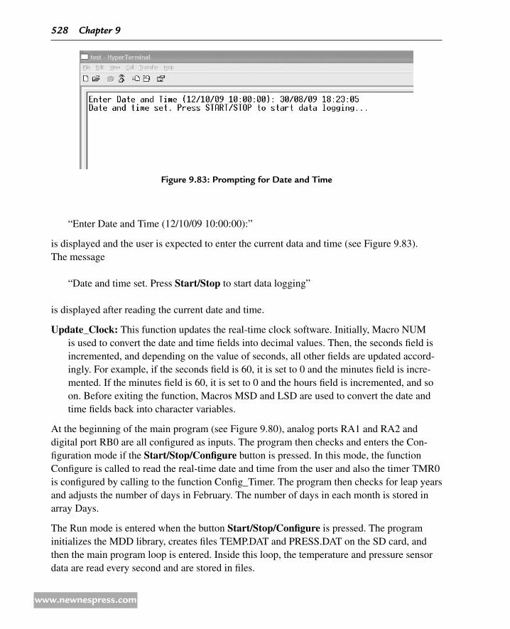
“Enter Date and Time (12/10/09 10:00:00):”
is displayed and the user is expected to enter the current data and time (see Figure 9.83). The message
“Date and time set. Press Start/Stop to start data logging”
is displayed after reading the current date and time.
Update_Clock: This function updates the real-time clock software. Initially, Macro NUM is used to convert the date and time fields into decimal values. Then, the seconds field is incremented, and depending on the value of seconds, all other fields are updated accord-ingly. For example, if the seconds field is 60, it is set to 0 and the minutes field is incre-mented. If the minutes field is 60, it is set to 0 and the hours field is incremented, and so on. Before exiting the function, Macros MSD and LSD are used to convert the date and time fields back into character variables.
At the beginning of the main program (see Figure 9.80), analog ports RA1 and RA2 and digital port RB0 are all configured as inputs. The program then checks and enters the Con-figuration mode if the Start/Stop/Configure button is pressed. In this mode, the function Configure is called to read the real-time date and time from the user and also the timer TMR0 is configured by calling to the function Config_Timer. The program then checks for leap years and adjusts the number of days in February. The number of days in each month is stored in array Days.
The Run mode is entered when the button Start/Stop/Configure is pressed. The program initializes the MDD library, creates files TEMP.DAT and PRESS.DAT on the SD card, and then the main program loop is entered. Inside this loop, the temperature and pressure sensor data are read every second and are stored in files.
Figure 9.83: Prompting for date and time
528 Chapter 9
www.newnespress.com
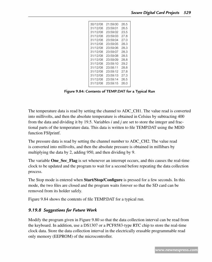
The temperature data is read by setting the channel to ADC_CH1. The value read is converted into millivolts, and then the absolute temperature is obtained in Celsius by subtracting 400 from the data and dividing it by 19.5. Variables i and j are set to store the integer and frac-tional parts of the temperature data. This data is written to file TEMP.DAT using the MDD function FSfprintf.
The pressure data is read by setting the channel number to ADC_CH2. The value read is converted into millivolts, and then the absolute pressure is obtained in millibars by multiplying the data by 2, adding 950, and then dividing by 9.
The variable One_Sec_Flag is set whenever an interrupt occurs, and this causes the real-time clock to be updated and the program to wait for a second before repeating the data collection process.
The Stop mode is entered when Start/Stop/Configure is pressed for a few seconds. In this mode, the two files are closed and the program waits forever so that the SD card can be removed from its holder safely.
Figure 9.84 shows the contents of file TEMP.DAT for a typical run.
9198 suggestions for Future Work
Modify the program given in Figure 9.80 so that the data collection interval can be read from the keyboard. In addition, use a DS1307 or a PCF8583-type RTC chip to store the real-time clock data. Store the data collection interval in the electrically erasable programmable read only memory (EEPROM) of the microcontroller.
30/12/08 21:59:00 26.531/12/08 23:59:01 26.531/12/08 23:59:02 23.531/12/08 23:59:03 27.831/12/08 23:59:04 27.031/12/08 23:59:05 28.331/12/08 23:59:06 28.331/12/08 23:59:07 28.331/12/08 23:59:08 28.531/12/08 23:59:09 28.831/12/08 23:59:10 29.231/12/08 23:58:11 28.831/12/08 23:59:12 27.831/12/08 23:59:13 27.331/12/08 23:59:14 26.531/12/08 23:59:15 26.0
Figure 9.84: Contents of teMP.dat for a typical run
secure Digital Card Projects 529
www.newnespress.com

This page intentionally left blank
Appendix A–MC33269 Data sheet
531

This page intentionally left blank

Appendix B–MAX232 Data sheet
533

This page intentionally left blank
Appendix C–LM35 Data sheet
535

This page intentionally left blank

Appendix D–MPX4115A Data sheet
537

This page intentionally left blank
Index
AAcquisition time, 89–91Address bus, 6Analog comparator, 10Analog-to-digital (A / D) converter,
8–9, 84, 86, 245–247analog input model of, 89–91bipolar, 84clock sources, 89conversion process, 85unipolar, 84
Arithmetic operators, 168–169Arrays, 161–162
passing to functions, 199–200pointers, 163–164
Assemblers, 258Assembly language, 258
statements, 187–188Assignment operators, 172–173
BBaud rate, 240, 479BCD numbers. See Binary-coded
decimal numbersBIGPIC4 development kit,
270–271Binary numbers, 13–14
adding, 26–27converting into decimal,
14–16converting into
hexadecimal, 18–19converting into octal, 24division, 29multiplication, 28–29subtracting, 27–28
Binary-coded decimal (BCD) numbers, 36–37packed, 36–37
Bipolar A / D converters, 84Bitwise operators, 171–172Breadboards, 283–285Break statement, 186–187Brown-out detector, 8bufr, 487Buses, 6
CC compilers, 258
CCS C compiler, 137mikroC C compiler, 137MPLAB C18 compiler.
See MPLAB C18 compiler
for PIC18 microcon-trollers, 137–138
PICC18 C compiler, 137C18 compiler. See MPLAB C18
compilerCapture mode, 77–79, 81Capture/compare/PWM (CCP)
modules, 77–80Card reset state, 135CCS C compiler, 137Central processing unit (CPU), 4Character classification
functions, 211–212example, 212
Character output functions, 218–219examples, 20, 219–221
CID register, 123–125Clock, 7Clock frequency with RC, 61Clock sources, 56–62
crystal/ceramic resonator as, 58–59
external, 59–60
resistor/capacitor operation, 60–61
Commands, SD card, 133Compact flash (CF) card, 110–111
advantages of, 110speeds of, 110, 111
Compare mode, 79–81Compilers, 258
C language, 258high-level language, 260
Complex instruction set computer (CISC), 12
Conditional operators, 173Config_Timer, 527Configuration files, 424–426Configuration registers, of
PIC18F452, 49–50, 52, 53Constants
character, 158character array, 158enumeration, 159floating point, 158integer, 157–158string, 158–159
Continue statement, 186Control bus, 6Control unit (CU), 4Controller area network (CAN)
interface, 11CPU. See Central processing unitCSD register, 125–130Current sink /source capability, 11
DData bus, 6Data conversion functions, 213
example, 213, 214Data logging, temperature. See
Temperature data logging
539

Data memory organization of PIC18F452, 49, 50
Data read, 132Data tokens, 134–135Data write, 132–133DataBuffer, 400Daughter SD card board, 415DC56-11EWA pin
configuration, 334, 335Debugger powered mode, 286Debugging
process, 288requirements for, 287set up, 286
Decimal number system, 13converting into binary,
16–17converting into floating
point, 33–34converting into hexadeci-
mal, 21converting into octal, 22–23
Delay functions, 207, 228for 4-MHz and 8-MHz
Clock, 229for 2400 baud with 4-MHz
Clock, 242flashing LED example
program, 208–211Deleting file, 439
operation, 439program code, 440–441
Development boards, 260BIGPIC4 development
kit, 270–271FUTURELEC PIC18F458
training board, 272LAB-XUSB experimenter
board, 261–262MK-1 Universal PIC
board, 265–266PIC18F4520 development
kit, 269–270PICDEM 2 plus board,
262–263PICDEM 4 board, 263–264PICDEM HPC explorer
board, 264PICDEM PIC18 EXPLORER
demonstration board, 273–274
SSE452 board, 266–267SSE8680 board, 268–269SSE8720 board, 267–268
Digital data logging to SD card, 502block diagram, 503circuit diagram, 504operation of, 505program code, 503–506
Directorycreating, 443–445
operation, 444program code, 445
and file, creatingdescription, 446operation, 446program code,
447–448Displaying attributes of file, 472
description, 472operation, 473program code, 473–476
Displaying file on PC, 451block diagram, 452circuit diagram, 452–453description, 451operation, 453program code, 453–457
Do statement, 185DSR register, 130Dynamic random access memory
(DRAM), 4
EEasyProg PIC programmer, 275,
276Eight-bit microcontrollers, 4Eight-bit mode, timer 0 in, 72Electrically erasable program-
mable read only memory (EEPROM), 5, 9
Embedded controllers, 1Erasable programmable read only
memory (EPROM), 5Escapes sequences, 159Ethernet interface, 11eXtended capacity (SDXC), 113
FFAT16 file system, 395FAT32 file system, 395
FATBuffer, 400Files
deleting, 439–441directories and, 446–448file copying, 448–451
description, 448operation, 449program code, 450–451
with given file extension, looking for, 467description, 467operation, 468program code, 468–472
handling operations, 477–488command mode, 477command options,
477–478program for, 477–479Read_Filename function
in, 478Read_SrcDst function
in, 479looking for, 463–467
description, 463operation, 463program code, 463–466
renaming, 441–443FindFirst function, 498Flash EEPROM, 6Flash memory card. See Memory
cardFlashing LED program, 150–151,
208–211, 289–292Floating point numbers, 30–31
addition and subtraction, 35–36
converting decimal number into, 33–34
converting into decimal, 31–32
mantissa, 30multiplication and
division, 34–35normalizing, 32
For statement, 181–183Forest electronics USB
programmer, 274Formatting card, 436–438
operation, 437program code, 437–438
540 Index
FSConfig.h, modifying, 399Function calls
FindFirst, 408–409, 486FindFirstpgm, 409FindNext, 410, 486FSchdir, 406–407,
486, 497FSerror, 500, 502FSfclose, 403FSfeof, 403FSfopen, 402, 487FSfopenpgm, 402–403FSformat, 407, 487FSfprintf, 410–411FSfread, 404FSfwrite, 404–406FSInit, 401–402FSmkdir, 487FSremove, 405,
486, 497FSremovepgm, 405FSrename, 407, 487FSrewind, 405FSrmdir, 406, 487sequence
deleting existing file, 401reading from existing
file, 400writing onto existing
file, 401SetClockVars, 410
Functions, 193–194to calculate area of
circle, 194–196to calculate cylinder area and
volume, 196, 197, 195to convert lowercase to
uppercase, 195, 197, 198, 200
definition, 193examples, 194–198passing arrays to, 199–200
examples, 200–204passing variables by reference
to, 204example, 204, 205
prototypes, 198–199static variables, 204–205void, 152, 193, 194
FUTURELEC PIC18F458 training board, 272
GGlobal interrupt enable bit
(GIE), 96Goto statement, 186Graphical user interface
(GUI), 260
HHardware development tools
breadboards, 283–285development boards.
See Development boardsdevice programmers, 274–275in-circuit debuggers, 276–280in-circuit emulators,
280–283Hardware peripheral library
functions, 206A / D converter, 245–247input capture, 247integrated interconnect (I2C)
bus, 247I/O port, 247microwire bus, 247pulse width modulation, 247serial peripheral interface
(SPI) bus, 248timer, 248–249universal synchronous-
asynchronous receiver-transmitter (USART), 249–252
HardwareProfile.h, modifying, 399Harvard architecture, 11, 12HD44780 LCD controller, 226–227
pin configuration and pin functions of, 227
Hexadecimal number system, 14converting into binary, 19–20converting into decimal, 20
High-capacity SD (SDHC) card, 113, 115–116
High-level languagecompilers, 260simulators, 259–260
IICD. See In-circuit debuggersICE. See In-circuit emulatorsICEPIC 3, 281, 282
IDEs. See Integrated development environments
IDL-800 Digital Lab, 285IEEE standard, 30If statement, 178–179In-circuit debuggers (ICD), 276–280
ICD-U40, 278, 279PICFlash-2 ICD, 278–279
In-circuit emulators (ICE), 280–283Instruction cycle, 7Integrated development
environments (IDEs), 260Integrated interconnect (I2C)
bus, 239, 247Internal clock control registers,
62, 63Interrupt service routine (ISR),
8, 340Interrupt vector address, 8Interrupts, 8, 91, 97
applications, 92bit definitions of registers,
97core and peripheral
sources, 92enabling/disabling, 94–96priority structure, 96–103
I/O portsfunctions in hardware, 247PIC microcontroller, 188
Iteration statementsdo statement, 185goto statement, 186for statement, 181–183while statement, 183–185
LLAB-XUSB experimenter
board, 261–262LCD. See Liquid crystal displayLED. See Light-emitting diodesLibrary functions, MPLAB C18,
206–207. See also specific library functions
Light-emitting diodes (LED)chasing, project
circuit diagram, 305description, 304hardware of, 305PDL of, 306program listing, 307, 306
Index 541

Light-emitting diodes (LED) (cont’d)dice project, 308
block diagram, 309circuit diagram, 309description, 308hardware, 308PDL of, 310program, 310–311
flashing, program, 150–151, 208–211, 289, 290–292
two-dice project, 314block diagram, 315circuit diagram, 315description, 314–315,
318–319hardware, 315, 319–321PDL of, 316, 321program, 316–318, 321using I/O pins, 318–326
Liquid crystal display (LCD), 225 See also HD44780 LCD controllerdrivers, 10functions, 225–226,
228, 232BusyXLCD, 228–230examples, 233–235,
237–239OpenXLCD, 230putcXLCD, 231putrsXLCD, 231putsXLCD, 231WriteCmdXLCD,
232–233parallel, 226serial, 226
LM35 precision centigrade temperature sensors, 535
Logical operators, 170Low-power operation, 10
MMach X programmer, 274–275Master synchronous serial port
(MSSP) module, 361configuration of, 365–367in SPI mode, 361–362
Math library functions, 207, 222, 223examples, 223–225
MAX232 dual EIA-232 drivers/receivers, 533
MC33269 low dropout three- terminal voltage regulators, 531
MC33269DT3-3 regulator, 429, 430
MDD. See Memory disk drive library
Melabs U2 Programmer, 275, 276
Memory and string manipulation functions, 213examples, 214–217
Memory card, 107applications, 107properties of
physical, 117technical, 117
technologies of, 108types of, 108
Memory card readers, 116Memory disk drive (MDD) library
data memory usage, 398file and disk manipulation
functions, 396installation, 395–396MPLAB C18 memory
usage, 398options, 396–398setup, 399–400
Memory model, 426Memory stick (MS) card, 111MENU-based SD card file
handling, 490block diagram, 452circuit diagram, 452operation of, 491program code, 491–502
Microchip daughter SD card board, 415
Microchip memory disk drive (MDD), 413
Microchip solutions, 396Microcomputer, 2Microcontroller
A / D converter, 8–9analog comparator, 10architectures, 11–12assembly languages, 2brown-out detector, 8buses, 6CAN interface, 11
choosing for application, 12clock, 7current sink /source
capability, 11defined, 1difference in
microprocessor, 1EEPROM, 5, 9EPROM, 5Ethernet interface, 11features, 6–11flash EEPROM, 6interrupts, 8LCD drivers, 10low-power operation, 10motor control interface, 11PIC18F452, 4–6pins, 428power-on reset, 10PROM, 5RAM, 4real-time clock, 10reset input, 8ROM, 5serial I/O, 9sleep mode, 10supply voltage, 6–7systems, 1–4temperature data logger
system, 2, 3timers, 7USB interface, 11watchdog, 7–8ZigBee interface, 11
Microdrive, 112Microprocessor, difference in
microcontroller, 1microSD card, 114mikroC C compiler, 137miniSD card, 114, 115MK-1 Universal PIC development
board, 265–266Motor control interface, 11MPLAB C18 compiler, 138
arrays, 161–162basic structure of, 152, 153case sensitivity, 154comments, 152–154compiler files, 142constants, 157–159control statements, 178
542 Index

directory, 139enumerated variables, 160environment variables, 140escapes sequences, 159example program
building the project, 143–147
flashing LED program, 150–151
simulating the project, 147–150
external variables, 160installing, 138–142library functions, 206–207,
367–369memory usage, 398mixing with assembly
language statements, 187–188
operators, 168–177pointers, 162–164programming examples,
189–192static variables, 160structures, 164–167terminating program
statements, 154unions, 167–168variable names, 155variable types, 155–157volatile variables, 160white spaces, 154
MPLAB C18 template, creating, 417configuration files
setting, 424–426memory model setting, 427
MPLAB ICD2, 278MPLAB ICD3, 279–280
connection of, 287debugger, 289–292debugging
examples, 292–295process, 288
modes of operation, 286test interface board, 289using, 285–288
MPLAB ICE 4000, 281MPLAB IDE
C18 directory structure, 142installing, 138
options, 141starting, 143
MPX4115A pressure sensors, 525, 537
MSSP. See Master synchronous serial port
Multimedia card (MMC), 109Multiplexed seven-segment
LED counterfour-digit with timer
interrupt, 347circuit diagram, 348description, 347hardware, 347PDL, 348, 349program, 348–352
two-digit, 333block diagram, 335circuit diagram, 336description, 333hardware, 335PDL, 335–336program, 337–338
two-digit with timer interrupt, 338description, 338–340hardware, 341modified program,
345–347PDL, 341program, 341–344
NNAND technology, 108Negative numbers, 25–26NOR technology, 108
OOCR register, 123, 124Octal number system, 14
converting into binary, 24converting into decimal,
21–22One time programmable
(OTP) memory, 5Operators in C18 language
arithmetic, 168–169assignment, 172–173bitwise, 171–172conditional, 173logical, 170
preprocessor, 173–177relational, 169–170
PPC display, 489PDL. See Program description
languagePIC microcontroller
flashing LED program, 208–211
I/O port programming, 188SD card interface, 122
PIC prog plus programmer, 275, 277
PIC programmer module, 275, 277PIC16 microcontroller series, 41PIC18 microcontrollers,
C programming languages for, 137–138
PIC18F microcontroller series, 41features of, 41, 44interrupts in, 93I/O ports, 63PIC16F and, 44
PIC18F452 microcontroller, 4–6, 45, 46A / D converter, 84–91clock sources on, 56–62configuration bits, 177configuration registers, 49–50,
52, 53data memory organization,
49, 50interrupts, 91, 97pin configuration of, 45ports, 47
PORTA pin, 64–66PORTB pin, 66–68PORTC pin, 67–69PORTD pin, 70PORTE pin, 70
power supply, 50–51, 55program memory
organization, 47–49reset, 53–57timers, 69–77
PIC18F4520 development kit, 269–270
PIC18FXX2 microcontroller family, 43architecture, 43, 44
Index 543

PICC18 C compiler, 137PICDEM 2 plus development
board, 262–263PICDEM 4 development
board, 263–264PICDEM HPC explorer
development board, 264PICDEM PIC18 EXPLORER
demonstration board, 273–274
PICDEM PIC18 Explorer demonstration board, 413, 414features, 414
PICE-MC, 282–283PICFlash-2 ICD, 278–279PICtail daughter board.
See Microchip daughter SD card board
Pointers, 162–164array, 163–164incrementing, 164
Power supply of PIC18F452, 50–51, 55
Power-on reset (POR), 10, 56–57Preprocessor commands, 174–176
#define, 152, 174#include, 152, 175#pragma, 176–177
Preprocessor operators, 173–177Program description language
(PDL) keywords, 299–304Do and ENDDO, 301–303IF-THEN-ELSE-ENDIF,
301, 302REPEAT-UNTIL, 303–304START-END, 300
Program memory map of PIC18F452, 47, 48
Programmable read only memory (PROM), 5
Pseudorandom number generator, 311–314
Pulse width modulation (PWM), 80–84, 247
RRandom access memory (RAM), 4RCA register, 130RCON register, 94Read only memory (ROM), 5
Read_ADC function, 526Read_Filename function, 478Reading filename from PC and
displaying file, 458–463description, 458operation of, 459program code, 460–462
Read_SrcDst function, 479, 487–500
Real-time clock (RTC), 3, 10Reduced instruction set computer
(RISC), 12Register bits
CONFIG1H, 54CONFIG2H, 55CONFIG2L, 54
Relational operators, 169–170Renaming file, 441
operation, 442program code, 442–443
Reset functions, 216, 217 example, 217, 218
Reset input, 8Resistor/capacitor operation,
60–61Response tokens, 133–134RICE3000, 281, 282RS232-based serial
communication, 239, 240, 24925-way and 9-way
connectors, 240, 453bit timing in, 240I/O, 9pins required for, 241
SSA52-11 pin configuration, 329SCR register, 131SearchRec structure, 409Secure digital (SD) card, 113–116
bus mode, 118, 119capacity, calculation,
131–132commands, 133high-capacity, 115–116interface, 119–122internal registers, 122–131pins, 428
assignments, 120configuration, 118–120
in SD bus mode, 118, 119
sizes of, 113–115in SPI bus mode, 118, 120standard. See Standard SD cardstatus register, 131structure of, 118–122writing short text message
to, 427block diagram, 428circuit diagram, 428–429description, 427modified program,
432–433operation, 430program code, 431–432
Selection statementsif statement, 178–179switch statement, 179–181
Serial communication. See RS232-based serial communication
Serial peripheral interface (SPI) bus, 248mode, 120, 118
MSSP in, 361–362operation, 365–367registers, 362–364
MPLAB C18 library functions, 239, 248, 367–369
project, 369, 370, 375 protocol, 132–134, 361
Serial port parameters, 457, 458SetClockVars function, 410Seven-segment LED counter,
326, 329circuit diagram, 329common anode
configuration, 327common cathode
configuration, 327description, 326–328hardware, 328–329modified program, 332–333PDL, 330program, 330
Signal conditioning, 84, 85Simulators, 257, 259
high-level language, 259–260Sixteen-bit mode, timer 0
in, 73, 74Sleep mode, 10Smart media (SM) card, 108–109
544 Index
Software development tools, 257–260assemblers/compilers,
258–259high-level language
simulators, 259–260IDEs, 260simulators, 257, 259text editors, 258
Software peripheral library functions, 206CAN2510, 239integrated interconnect (I2C)
bus, 239LCD. See Liquid crystal
display (LCD), functionsserial peripheral interface
(SPI) bus, 239UART, 239–243
example, 243–245Solid state floppy disc card
(SSFDC), 108Source-level debuggers, 259Special function register (SFR),
49, 51SPI. See Serial peripheral interfaceSSE452 development board,
266–267SSE8680 development board,
268–269SSE8720 development board,
267–268SSPCON1 register, 364SSPSTAT register, 363–364Standard SD card, 113–115
modes of, 118voltage levels of, 119, 121
Static random access memory (SRAM), 4
strcmppgm2ram function, 485Structures, 164–167Supply voltage, 6–7Switch statement, 179–180
example using, 180–181
TTarget powered mode, 286TC72 temperature sensor,
370–371
block diagram, 370circuit diagram, 374, 375features of, 370internal registers of, 372–373MSB and LSB settings of, 371pin configuration of, 370program, 374–381
to displaying fractional part, 382, 387–392
to displaying negative temperatures, 381–387
read/write operations, 372Temperature and pressure data
logging with real-time clock, 515block diagram, 517circuit diagram, 516, 517operation of, 518program code, 516–529
Temperature data logging, 507block diagram, 508circuit diagram, 507, 508operation of, 509program code, 509–514system, 2, 3
Text editors, 258Time stamping file, 433
operation of, 434program code, 435–436
Timer library routines, 352–359
Timer_ISR function, 526Timers, 7, 69
Timer 0, 71–73Timer 1, 73–76Timer 2, 73–77Timer 3, 77, 79
Typedef statements, 166
UUnions, 167–168Unipolar A / D converters, 84Universal asynchronous
receiver-transmitter (UART) functions, 239–243example, 243–245OpenUART, 241–242putsUART, 243
ReadUART, 242WriteUART, 242
Unions, 167–168Unipolar A / D converters, 84Universal serial bus (USB)
interface, 11Universal synchronous-asynchronous
receiver-transmitter (USART) function, 9, 249–252baudUSART, 252BusyUSART, 250CloseUSART, 250DataRdyUSART, 250getcUSART, 250getsUSART, 250Init_USART, 527OpenUSART, 250putcUSART, 252putrsUSART, 252putsUSART, 252
Update_Clock function, 528USB programmer, Forest
electronics, 274
VVariables
enumerated, 160environment, 140external, 160names, 155static, 160, 204–205types, 155–157volatile, 160
Void, 152, 193, 194Von Neumann architecture,
11, 12
WWatchdog timer (WDT), 7–8,
62–63While statement, 183–185,
486–488WriteTimer0, 359
XxD card, 112–113
ZZigBee interface, 11
Index 545

This page intentionally left blank


